EP3451547A1 - Modem and electronic device - Google Patents
Modem and electronic device Download PDFInfo
- Publication number
- EP3451547A1 EP3451547A1 EP18190917.7A EP18190917A EP3451547A1 EP 3451547 A1 EP3451547 A1 EP 3451547A1 EP 18190917 A EP18190917 A EP 18190917A EP 3451547 A1 EP3451547 A1 EP 3451547A1
- Authority
- EP
- European Patent Office
- Prior art keywords
- modem
- terminal device
- loop antenna
- data
- communicator
- Prior art date
- Legal status (The legal status is an assumption and is not a legal conclusion. Google has not performed a legal analysis and makes no representation as to the accuracy of the status listed.)
- Granted
Links
Images




Classifications
-
- H—ELECTRICITY
- H04—ELECTRIC COMMUNICATION TECHNIQUE
- H04W—WIRELESS COMMUNICATION NETWORKS
- H04W4/00—Services specially adapted for wireless communication networks; Facilities therefor
- H04W4/80—Services using short range communication, e.g. near-field communication [NFC], radio-frequency identification [RFID] or low energy communication
-
- H—ELECTRICITY
- H04—ELECTRIC COMMUNICATION TECHNIQUE
- H04L—TRANSMISSION OF DIGITAL INFORMATION, e.g. TELEGRAPHIC COMMUNICATION
- H04L41/00—Arrangements for maintenance, administration or management of data switching networks, e.g. of packet switching networks
- H04L41/08—Configuration management of networks or network elements
- H04L41/0866—Checking the configuration
- H04L41/0869—Validating the configuration within one network element
-
- H—ELECTRICITY
- H02—GENERATION; CONVERSION OR DISTRIBUTION OF ELECTRIC POWER
- H02J—ELECTRIC POWER NETWORKS; CIRCUIT ARRANGEMENTS OR SYSTEMS FOR SUPPLYING OR DISTRIBUTING ELECTRIC POWER; SYSTEMS FOR STORING ELECTRIC ENERGY
- H02J50/00—Circuit arrangements or systems for wireless supply or distribution of electric power
- H02J50/10—Circuit arrangements or systems for wireless supply or distribution of electric power using inductive coupling
-
- H—ELECTRICITY
- H02—GENERATION; CONVERSION OR DISTRIBUTION OF ELECTRIC POWER
- H02J—ELECTRIC POWER NETWORKS; CIRCUIT ARRANGEMENTS OR SYSTEMS FOR SUPPLYING OR DISTRIBUTING ELECTRIC POWER; SYSTEMS FOR STORING ELECTRIC ENERGY
- H02J1/00—Circuit arrangements for DC mains or DC distribution networks
- H02J1/10—Parallel operation of DC sources
- H02J1/108—Parallel operation of DC sources having arrangements for blocking reverse current flow, e.g. using diodes
-
- H—ELECTRICITY
- H04—ELECTRIC COMMUNICATION TECHNIQUE
- H04B—TRANSMISSION
- H04B1/00—Details of transmission systems, not covered by a single one of groups H04B3/00 - H04B13/00; Details of transmission systems not characterised by the medium used for transmission
- H04B1/38—Transceivers, i.e. devices in which transmitter and receiver form a structural unit and in which at least one part is used for functions of transmitting and receiving
- H04B1/40—Circuits
-
- H—ELECTRICITY
- H04—ELECTRIC COMMUNICATION TECHNIQUE
- H04B—TRANSMISSION
- H04B3/00—Line transmission systems
- H04B3/54—Systems for transmission via power distribution lines
- H04B3/544—Setting up communications; Call and signalling arrangements
-
- H—ELECTRICITY
- H04—ELECTRIC COMMUNICATION TECHNIQUE
- H04B—TRANSMISSION
- H04B5/00—Near-field transmission systems, e.g. inductive or capacitive transmission systems
- H04B5/20—Near-field transmission systems, e.g. inductive or capacitive transmission systems characterised by the transmission technique; characterised by the transmission medium
- H04B5/24—Inductive coupling
- H04B5/26—Inductive coupling using coils
-
- H—ELECTRICITY
- H04—ELECTRIC COMMUNICATION TECHNIQUE
- H04B—TRANSMISSION
- H04B5/00—Near-field transmission systems, e.g. inductive or capacitive transmission systems
- H04B5/20—Near-field transmission systems, e.g. inductive or capacitive transmission systems characterised by the transmission technique; characterised by the transmission medium
- H04B5/24—Inductive coupling
- H04B5/26—Inductive coupling using coils
- H04B5/263—Multiple coils at either side
-
- H—ELECTRICITY
- H04—ELECTRIC COMMUNICATION TECHNIQUE
- H04B—TRANSMISSION
- H04B5/00—Near-field transmission systems, e.g. inductive or capacitive transmission systems
- H04B5/20—Near-field transmission systems, e.g. inductive or capacitive transmission systems characterised by the transmission technique; characterised by the transmission medium
- H04B5/24—Inductive coupling
- H04B5/26—Inductive coupling using coils
- H04B5/266—One coil at each side, e.g. with primary and secondary coils
-
- H—ELECTRICITY
- H04—ELECTRIC COMMUNICATION TECHNIQUE
- H04B—TRANSMISSION
- H04B5/00—Near-field transmission systems, e.g. inductive or capacitive transmission systems
- H04B5/70—Near-field transmission systems, e.g. inductive or capacitive transmission systems specially adapted for specific purposes
- H04B5/79—Near-field transmission systems, e.g. inductive or capacitive transmission systems specially adapted for specific purposes for data transfer in combination with power transfer
-
- H—ELECTRICITY
- H04—ELECTRIC COMMUNICATION TECHNIQUE
- H04M—TELEPHONIC COMMUNICATION
- H04M11/00—Telephonic communication systems specially adapted for combination with other electrical systems
- H04M11/06—Simultaneous speech and data transmission, e.g. telegraphic transmission over the same conductors
-
- H—ELECTRICITY
- H04—ELECTRIC COMMUNICATION TECHNIQUE
- H04W—WIRELESS COMMUNICATION NETWORKS
- H04W4/00—Services specially adapted for wireless communication networks; Facilities therefor
- H04W4/30—Services specially adapted for particular environments, situations or purposes
-
- H—ELECTRICITY
- H04—ELECTRIC COMMUNICATION TECHNIQUE
- H04W—WIRELESS COMMUNICATION NETWORKS
- H04W84/00—Network topologies
- H04W84/02—Hierarchically pre-organised networks, e.g. paging networks, cellular networks, WLAN [Wireless Local Area Network] or WLL [Wireless Local Loop]
- H04W84/10—Small scale networks; Flat hierarchical networks
- H04W84/14—WLL [Wireless Local Loop]; RLL [Radio Local Loop]
-
- H—ELECTRICITY
- H04—ELECTRIC COMMUNICATION TECHNIQUE
- H04W—WIRELESS COMMUNICATION NETWORKS
- H04W88/00—Devices specially adapted for wireless communication networks, e.g. terminals, base stations or access point devices
- H04W88/02—Terminal devices
-
- H—ELECTRICITY
- H01—ELECTRIC ELEMENTS
- H01Q—ANTENNAS, i.e. RADIO AERIALS
- H01Q1/00—Details of, or arrangements associated with, antennas
- H01Q1/12—Supports; Mounting means
- H01Q1/22—Supports; Mounting means by structural association with other equipment or articles
- H01Q1/24—Supports; Mounting means by structural association with other equipment or articles with receiving set
- H01Q1/241—Supports; Mounting means by structural association with other equipment or articles with receiving set used in mobile communications, e.g. GSM
Definitions
- the above-described modem may further include a battery connected in parallel to an output of the power supply.
- At least one of the wireless communicator, the wired communicator, and the controller may be configured to operate by the power generated by the power supply and power of the battery.
- the power supply and the battery connected in parallel to each other may be connected to the booster circuit.
- the field device FD described above is, for example, a sensor device such as a flow meter or a temperature sensor, a valve device such as a flow rate control valve or an open/close valve, an actuator device such as a fan or a motor, an imaging device such as a camera or video equipment for imaging situations or objects in the plant, audio devices such as a microphone and a speaker for collecting abnormal sounds or the like and issuing an alarm sound or the like in the plant, a position detecting device for outputting position information of each device, or other devices.
- a sensor device such as a flow meter or a temperature sensor
- a valve device such as a flow rate control valve or an open/close valve
- an actuator device such as a fan or a motor
- an imaging device such as a camera or video equipment for imaging situations or objects in the plant
- audio devices such as a microphone and a speaker for collecting abnormal sounds or the like and issuing an alarm sound or the like in the plant
- a position detecting device for outputting position information of each device, or
- the antenna module 31 is arranged in the inner space of the magnetic member 33 such that the bottom plate member 33a is positioned on the -Z side, the side plate member 33b is positioned on the -X side, the side plate member 33c is positioned on the +X side, and the side plate member 33d is positioned on the -Y side, and the side plate member 33e is positioned on the +Y side.
- This arrangement allows electromagnetic fields acting on the loop antenna 21 to be formed along the bottom plate member 33a and the side plate members 33b, 33c, 33d, and 33e that constitute the magnetic member 33. Therefore, it is possible to obtain magnetic field characteristics equal to or better than those of a free space even under shielding by the conductive case 35.
Landscapes
- Engineering & Computer Science (AREA)
- Computer Networks & Wireless Communication (AREA)
- Signal Processing (AREA)
- Power Engineering (AREA)
- Near-Field Transmission Systems (AREA)
- Cable Transmission Systems, Equalization Of Radio And Reduction Of Echo (AREA)
- Transceivers (AREA)
- Arrangements For Transmission Of Measured Signals (AREA)
Abstract
Description
- The present invention relates to a modem and an electronic device.
- The present application claims priority based on Japanese patent application
2017-164618, filed on August 29, 2017 - Generally, in a plant, a factory, or the like (hereinafter referred to as a "plant"), an operator performs maintenance work at regular or irregular intervals from the viewpoints of prevention of abnormal operation, maintenance of performance, and the like. For example, maintenance work such as inspection or maintenance of field equipment (measuring devices or operating devices) which are called field devices is performed in a plant in which a distributed control system (DCS) is constructed.
- Maintenance of a field device is often performed using a terminal device such as a computer or a personal digital assistant (PDA) on which a dedicated tool (a field device setting tool) for setting and adjusting the field device is installed. A modem is sometimes used to communicatively connect such a terminal device to a field device. When the terminal device and the field device are communicatively connected through the modem, the terminal device can read various parameters set in the field device and can perform setting of new parameters or the like for the field device.
- "Technical Data Sheet VIATOR Bluetooth IF", [online], MACTek, [accessed on July 13, 2017], Internet <URL: https: //www.mactekcorp.com/downloads/Technical_Data_Sheet_VIATOR_Bluetooth_IF_Mod el_010041.zip> (hereinafter referred to as "Non-Patent
Document 1") discloses a modem that meets intrinsically safe explosion-proof standards and can perform Bluetooth (registered trademark) communication (hereinafter referred to as "BT communication"). Specifically, the modem disclosed in Non-PatentDocument 1 includes a main body that houses a communication circuit for performing BT communication, a modem circuit, and a battery for driving these circuits, and two cables that connect the modem circuit of the main body to a field device. When such a modem is used, BT communication is performed between the terminal device and the modem and wired communication is performed between the modem and the field device via the cables, such that the terminal device and the field device are communicatively connected. - It is generally necessary for wireless devices to obtain a certification (a wireless standard certification) to comply with the laws and regulations of each country. For wireless portable devices which are used in environments filled with flammable gas and dust and are connected to intrinsically safe equipment, it is necessary to obtain a certification (an explosion-proof certification) to comply with explosion-proof standards based on an intrinsically safe explosion-proof structure in addition to the wireless standard certification described above. It is also necessary for the modem disclosed in Non-Patent
Document 1 to obtain a wireless standard certification and an explosion-proof certification since it may be used in environments where flammable gas is used. There is a need to obtain the wireless standard certification and the explosion-proof certification individually for each country or region. Therefore, even if the modem disclosed in Non-PatentDocument 1 has obtained a wireless standard certification and an explosion-proof certification in one country, it is necessary to obtain another explosion-proof certificate when a change has been made to obtain a wireless standard certification in another country. Thus, the large amount of time, costs, and personnel are required since a wireless standard certification and an explosion-proof certification need to be obtained individually for each country or region as described above. - The modem disclosed in Non-Patent
Document 1 can perform BT communication with a terminal device, is physically separated from the terminal device, and does not need to receive supply of power from the terminal device. Therefore, for example, as compared to a modem that is physically connected to a terminal device and needs to receive supply of power from the terminal device, it is possible to lower the power to a level required for Fieldbus communication, which is advantageous from the viewpoint of an explosion-proof structure. However, since it is necessary to provide a battery in the main body, it is necessary to replace the battery at certain time intervals (for example, every several months). Although it can be considered that replacing the battery becomes unnecessary when a secondary battery is provided in the main body such that the battery is rechargeable. However, the energy for recharging becomes a major problem in terms of an explosion-proof structure and also an increase in size and weight are incurred. - One aspect of the present invention provides a modem and an electronic device which can reduce the time required for certification while incurring no increase in size and weight.
- A modem configured to communicatively connect a terminal device to a field device according to a first aspect of the present invention may include a wireless communicator configured to operate by power supplied in a noncontact manner from the terminal device and to perform short-range wireless communication with the terminal device, a wired communicator configured to operate by power supplied in a noncontact manner from the terminal device and to perform wired communication with the field device, and a controller configured to operate by power supplied in a noncontact manner from the terminal device and to control data exchanged between the wireless communicator and the wired communicator.
- The above-described modem may further include a storage configured to operate by power supplied in a noncontact manner from the terminal device and storing first data for the field device received by the wireless communicator and second data for the terminal device received by the wired communicator. The controller may be configured to read and output the first data stored in the storage to the wired communicator and to store the second data received by the wired communicator into the storage.
- The above-described modem may further include a first loop antenna connected to the wireless communicator, and a magnetic member arranged to cover the first loop antenna except for one surface side of the first loop antenna.
- The above-described modem may further include a power supply configured to generate the power from an induced current that flows through the first loop antenna, the induced current being caused by the short-range wireless communication.
- The above-described modem may further include a second loop antenna arranged overlapping the first loop antenna. The power supply may be configured to generate the power from induced currents that flow through the first and second loop antennas, the induced currents being caused by the short-range wireless communication.
- The above-described modem may further include a battery connected in parallel to an output of the power supply.
- In the above-described modem, the one surface side of the first loop antenna which is not covered with the magnetic member may act as a transceiver and receiver which transfers and receives electromagnetic waves used for the short-range wireless communication. The modem may further include a housing, at least a surface of the housing except for the transceiver and receiver being formed of a conductive material.
- In the above-described modem, the storage may store status information including information indicating whether or not at least one of the first data and the second data is stored in the storage and information indicating the type of the at least one of the first data and the second data stored in the storage. The wireless communicator may be configured to read the status information stored in the storage in accordance with a read request received from the terminal device and to transmit the read status information to the terminal device.
- In the above-described modem, the modem may be mounted on the terminal device, the transceiver and receiver of the modem being in close contact with a position of the terminal device at which an antenna is attached to the terminal device.
- In the above-described modem, the first loop antenna and the second loop antenna may be concentric with each other.
- In the above-described modem, at least one of the wireless communicator, the wired communicator, and the controller may be configured to operate by the power generated by the power supply and power of the battery.
- The above-described modem may further include a booster circuit configured to boost output voltage of the power supply.
- In the above-described modem, a circuit including the power supply and the booster circuit, and the battery are connected in parallel.
- In the above-described modem, the power supply and the battery connected in parallel to each other may be connected to the booster circuit.
- An electronic device according to a second aspect of the present invention may include a terminal device including an antenna and configured to perform short-range wireless communication, and the above-described modem wherein the first loop antenna is disposed close to the antenna of the terminal device.
- According to the one aspect of the present invention, it is possible to reduce the time required for certification while incurring no increase in size and weight.
-
-
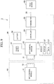
FIG. 1 is a block diagram showing a configuration of main parts of an electronic device according to a first embodiment of the present invention. -
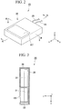
FIG. 2 is a perspective view showing an appearance of a modem according to the first embodiment of the present invention. -
FIG. 3 is a cross-sectional view taken along line A-A inFIG. 2 . -
FIG. 4 is a cross-sectional view taken along line B-B inFIG. 2 . -
FIG. 5 is a perspective view showing a magnetic member provided in the modem according to the first embodiment of the present invention. -
FIG. 6 is a cross-sectional view showing exemplary mounting of a modem according to the first embodiment of the present invention. -
FIG. 7 is a block diagram showing a configuration of main parts of an electronic device according to a second embodiment of the present invention. -
FIG. 8 is a diagram showing exemplary installation of loop antennas according to the second embodiment of the present invention. -
FIG. 9 is a block diagram showing a configuration of main parts of an electronic device according to a third embodiment of the present invention. -
FIGS. 10A and 10B are diagrams showing exemplary configurations of a connection circuit between a power supply and a battery according to a third embodiment of the present invention. -
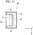
FIG. 11 is a cross-sectional view of a modem according to a fourth embodiment of the present invention. - Hereinafter, modems and electronic devices according to embodiments of the present invention will be described in detail with reference to the drawings. In the drawings referred to below, dimensions of members are appropriately changed for illustration as necessary for ease of understanding. In the following description, the positional relationship between each of the members will be described with reference to an XYZ orthogonal coordinate system set in the figures as necessary. The position of the origin in the XYZ orthogonal coordinate system is appropriately changed.
-
FIG. 1 is a block diagram showing a configuration of main parts of an electronic device according to a first embodiment of the present invention. As shown inFIG. 1 , theelectronic device 1 of the present embodiment includes aterminal device 10 and amodem 20. In such anelectronic device 1, short-range wireless communication is performed between theterminal device 10 and themodem 20 and wired communication is performed between themodem 20 and a field device FD, whereby theterminal device 10 and the field device FD are communicatively connected to each other. - The short-range wireless communication performed between the
terminal device 10 and themodem 20 is near field communication (NFC). NFC means communication (noncontact communication) which is possible when the distance between the devices which will communicate is, for example, several tens of cm or less and also includes communication performed in a state where housings of the devices which will communicate are in contact. The wired communication performed between themodem 20 and the field device FD is communication using a general purpose communication protocol for process industries such as HART (registered trademark), BRAIN, Foundation Fieldbus (registered trademark), or PROF1BUS (registered trademark). - The field device FD described above is, for example, a sensor device such as a flow meter or a temperature sensor, a valve device such as a flow rate control valve or an open/close valve, an actuator device such as a fan or a motor, an imaging device such as a camera or video equipment for imaging situations or objects in the plant, audio devices such as a microphone and a speaker for collecting abnormal sounds or the like and issuing an alarm sound or the like in the plant, a position detecting device for outputting position information of each device, or other devices.
- The
terminal device 10 includes anNFC control module 11 and a loop antenna 12 (an antenna), and performs short-range wireless communication (NFC) with themodem 20. Theterminal device 10 is realized by a portable computer of for example a notebook type or a tablet type. TheNFC control module 11 performs control of the short-range wireless communication with themodem 20 under the control of a control device (not shown) provided in theterminal device 10. For example, theNFC control module 11 performs control to read a status ST stored in amemory 23 of themodem 20 at predetermined time intervals (for example, every several milliseconds). The details of the status ST will be described later. The purpose of performing such control is to speed up bidirectional communication between theterminal device 10 and the field device FD via themodem 20 and to provide stable supply of power to themodem 20. - The
NFC control module 11 transmits data which is to be transmitted to the field device FD through theloop antenna 12 as a wireless signal and receives data from themodem 20 by detecting a load variation in theloop antenna 12. Theloop antenna 12 is connected to theNFC control module 11 as an antenna for transmitting and receiving wireless signals that are used in short-range wireless communication. As described above, theterminal device 10 transmits wireless signals at predetermined time intervals such that power is supplied to themodem 20 in a noncontact manner at predetermined time intervals. Therefore, theloop antenna 12 can be regarded as an antenna that transmits power to themodem 20 in a noncontact manner. Although the present embodiment will be described with regard to an example in which theterminal device 10 includes theloop antenna 12, the antenna included in theterminal device 10 is not limited to theloop antenna 12 as long as it enables short-range wireless communication with themodem 20. - The
modem 20 includes a loop antenna 21 (a first loop antenna), an NFC control module 22 (a wireless communicator), a memory 23 (a storage), acontroller 24, a communicator 25 (a wired communicator), acable 26, and apower supply 27. Themodem 20 performs short-range wireless communication with theterminal device 10 and performs the above-described wired communication with the field device FD. Each of the blocks (theNFC control module 22, thememory 23, thecontroller 24, and the communicator 25) in themodem 20 operates with power (precisely, DC power rectified and smoothed by the power supply 27) supplied in a noncontact manner from theterminal device 10. - The
loop antenna 21 is connected to theNFC control module 22 as an antenna for transmitting and receiving wireless signals that are used in short-range wireless communication. In order to realize short-range wireless communication with theterminal device 10, theloop antenna 21 is disposed close to theloop antenna 12 provided in theterminal device 10. As described above, themodem 20 receives wireless signals transmitted from theterminal device 10 at predetermined time intervals such that power is supplied to themodem 20 in a noncontact manner at predetermined time intervals. Therefore, theloop antenna 21 can be regarded as an antenna that receives power supplied in a noncontact manner from theterminal device 10. - The
NFC control module 22 operates with power supplied in a noncontact manner from theterminal device 10. TheNFC control module 22 receives data transmitted from theterminal device 10 and transmits data that is to be transmitted to theterminal device 10. TheNFC control module 22 transmits data that is to be transmitted to theterminal device 10 by causing a load variation corresponding to the data that is to be transmitted to theterminal device 10. That is, in short-range wireless communication performed between theterminal device 10 and themodem 20, wireless signals are spontaneously transmitted from theterminal device 10, whereas wireless signals are not spontaneously transmitted from themodem 20. - The
memory 23 operates with power supplied in a noncontact manner from theterminal device 10. Thememory 23 stores the data DT and the status ST (status information). As thismemory 23, a nonvolatile memory or a volatile memory may be used. The data DT includes data (first data) for the field device FD received by theNFC control module 22 and data (second data) for theterminal device 10 received by thecommunicator 25. The status ST is information indicating the status of themodem 20. The status ST includes, for example, information indicating whether or not data DT is stored in thememory 23 or information indicating the type of the data DT stored in thememory 23. The information indicating the type of the data DT includes, for example, information indicating whether the data DT is the first data or the second data described above. - The
controller 24 operates with power supplied in a noncontact manner from theterminal device 10. Thecontroller 24 controls data exchanged between theNFC control module 22 and thecommunicator 25. For example, theNFC control module 22 performs control to read and output the first data stored as data DT in thememory 23 to thecommunicator 25. Thecontroller 24 performs control to cause thememory 23 to store the second data received by thecommunicator 25 as data DT. - The
communicator 25 is connected to the field device FD via thecable 26. Thecommunicator 25 performs the above-described wired communication with the field device FD via thecable 26. Thecable 26 is one that connects thecommunicator 25 and the field device FD. Thiscable 26 may be directly connected to the field device FD or may be connected to a transmission line or a network. When thecable 26 is connected to a transmission line or a network, thecommunicator 25 is connected to the field device FD via thecable 26 and the transmission line or the network. - The
power supply 27 generates power to operate each of the blocks in the modem 20 (theNFC control module 22, thememory 23, thecontroller 24, and the communicator 25) by converting power (AC power) supplied in a noncontact manner from theterminal device 10 into DC power. For example, thepower supply 27 includes a rectifying circuit and a smoothing circuit. Thepower supply 27 rectifies and smooths an induced current that flows through theloop antenna 21 as short-range wireless communication is performed between theterminal device 10 and themodem 20, thereby converting the power (AC power) supplied in a noncontact manner from theterminal device 10 into DC power. Although the present embodiment will be described with regard to an example in which thememory 23 and thepower supply 27 are provided separately from theNFC control module 22, at least one of thememory 23 and thepower supply 27 may be provided in theNFC control module 22. -
FIG. 2 is a perspective view showing an appearance of the modem according to the first embodiment of the present invention.FIG. 3 is a cross-sectional view taken along line A-A inFIG. 2 andFIG. 4 is a cross-sectional view taken along line B-B inFIG. 2 . As shown inFIGS. 2 to 4 , themodem 20 of the present embodiment includes amain body 30 having a rectangular parallelepiped shape and twocables cables cable 26 shown inFIG. 1 . - The
main body 30 includes anantenna module 31, amodem circuit board 32, amagnetic member 33, aplastic case 34, and a conductive case 35 (a housing). Theantenna module 31 includes, for example, theloop antenna 21, theNFC control module 22, thememory 23, and thepower supply 27 shown inFIG. 1 . Theantenna module 31 is, for example, a plate-shaped module that mainly performs short-range wireless communication with theterminal device 10. Themodem circuit board 32 includes, for example, thecontroller 24 and thecommunicator 25 shown inFIG. 1 . Themodem circuit board 32 is, for example, a plate-shaped board that mainly performs wired communication with the field device FD. - The
antenna module 31 and themodem circuit board 32 are arranged in themodem 20 such that, for example, theantenna module 31 and themodem circuit board 32 are parallel to the XY plane and are arranged along the X axis such that theantenna module 31 is positioned on the +X side and themodem circuit board 32 is positioned on the -X side. As a result, theloop antenna 21 provided in theantenna module 31 is arranged such that a winding surface thereof is parallel to the XY plane. Theantenna module 31 and themodem circuit board 32 are electrically connected via a connector (not shown). - The
magnetic member 33 is arranged to cover theloop antenna 21 except for one surface side (the +Z side) of theloop antenna 21. The purpose of arranging themagnetic member 33 in this manner is to efficiently couple electromagnetic fields radiated from theloop antenna 12 of theterminal device 10 to theloop antenna 21 and to obtain magnetic field characteristics equal to or better than those of a free space even under shielding by theconductive case 35. A member formed of ferrite can be used as themagnetic member 33. Further, by inserting a metal plate on a back surface (the -Z side) of themagnetic member 33, it is possible to insert an electronic substrate between the back surface (the -Z side) of the metal plate and theconductive case 35 and to secure a larger installation area. -
FIG. 5 is a perspective view showing the magnetic member provided in the modem according to the first embodiment of the present invention. As shown inFIG. 5 , themagnetic member 33 is, for example, a bottomed rectangular ring-shaped member formed of a combination of a plate-shapedbottom plate member 33a and plate-shapedside plate members bottom plate member 33a. Thebottom plate member 33a is disposed, for example, in the XY plane. Theside plate members bottom plate member 33a, respectively. Theside plate members bottom plate member 33a, respectively. - As shown in
FIG. 5 , theantenna module 31 is arranged in the inner space of themagnetic member 33 such that thebottom plate member 33a is positioned on the -Z side, theside plate member 33b is positioned on the -X side, theside plate member 33c is positioned on the +X side, and theside plate member 33d is positioned on the -Y side, and theside plate member 33e is positioned on the +Y side. This arrangement allows electromagnetic fields acting on theloop antenna 21 to be formed along thebottom plate member 33a and theside plate members magnetic member 33. Therefore, it is possible to obtain magnetic field characteristics equal to or better than those of a free space even under shielding by theconductive case 35. - The
plastic case 34 is a case that houses theantenna module 31, themodem circuit board 32, and themagnetic member 33. Theplastic case 34 houses theantenna module 31, themodem circuit board 32, and themagnetic member 33 to prevent positional deviations of theantenna module 31, themodem circuit board 32, and themagnetic member 33. For example, theplastic case 34 may be molded together with theantenna module 31, themodem circuit board 32, and themagnetic member 33. - The
conductive case 35 is a case that covers theplastic case 34. Theconductive case 35 is formed of, for example, a conductive resin having a conductivity equivalent to that of a metal such as carbon fiber reinforced plastic (CFRP) or conductive ABS. Theconductive case 35 has a rectangular parallelepiped shape and has an opening portion formed in a part of the +Z side surface thereof (i.e., in a part thereof where the +Z side of theloop antenna 21 is positioned). The part where the opening portion is formed has a transmitting/receiving portion RT through which wireless signals used for short-range wireless communication are transmitted and received. The area of the transmitting/receiving portion RT is set to, for example, 400 mm2 or less due to explosion proof limitations. - The purpose of covering the
plastic case 34 with theconductive case 35 except for the transmitting/receiving portion RT is to satisfy explosion-proof standards. That is, when theplastic case 34 is not covered with theconductive case 35, there is a possibility that static electricity may be generated, for example, as the clothes of the worker handling themodem 20 rub against theplastic case 34. On the other hand, when theplastic case 34 is covered with theconductive case 35, generation of such static electricity is prevented, satisfying explosion-proof standards. The reason why the transmitting/receiving portion RT is not covered with theconductive case 35 is to secure the path for wireless signals to ensure short-range wireless communication. -
FIG. 6 is a cross-sectional view showing exemplary mounting of the modem according to the first embodiment of the present invention.FIG. 6 shows exemplary mounting when theterminal device 10 is a tablet computer. As shown inFIG. 6 , themodem 20 is mounted on theterminal device 10 such that the transmitting/receiving portion RT of themodem 20 is in close contact with a position of theterminal device 10 at which theloop antenna 12 is attached to theterminal device 10. Thereby, theloop antenna 12 of theterminal device 10 and the antenna module 31 (the loop antenna 21) of themodem 20 are disposed close to each other, enabling short-range wireless communication between theterminal device 10 and themodem 20. - As shown in
FIG. 6 , most of the periphery of the space between theloop antenna 12 of theterminal device 10 and the antenna module 31 (the loop antenna 21) of themodem 20 is covered with the magnetic member 33 (theside plate members FIG. 5 ) and the -Z side of theantenna module 31 of themodem 20 is also covered with the magnetic member 33 (thebottom plate member 33a shown inFIG. 5 ). As a result, it is possible to obtain magnetic field characteristics equal to or better than those of a free space even under shielding by theconductive case 35, enabling short-range wireless communication between theterminal device 10 and themodem 20. - Next, the operation of the
electronic device 1 having the above configuration will be described. An operation in which theterminal device 10 reads the status ST stored in thememory 23 of the modem 20 (hereinafter referred to as a "status reading operation"), an operation in which theterminal device 10 transmits data to the field device FD (hereinafter, referred to as a "data transmission operation"), and an operation in which theterminal device 10 receives data transmitted from the field device FD (hereinafter referred to as a "data reception operation") will be described below. - In the
terminal device 10, theNFC control module 11 is controlled by a control device (not shown). In theterminal device 10, under the control of theNFC control module 11, an operation of reading the status ST stored in thememory 23 of themodem 20 is performed at predetermined time intervals (for example, every several milliseconds). Thereby, a wireless signal indicating a request to read the status ST is transmitted from theloop antenna 12 of theterminal device 10 at predetermined time intervals. - The wireless signal transmitted from the
loop antenna 12 of theterminal device 10 is received by theloop antenna 21 of themodem 20. Since the wireless signal transmitted from theloop antenna 12 of theterminal device 10 is shielded by themagnetic member 33 provided in themodem 20, the wireless signal is prevented from being radiated to the outside. When theloop antenna 21 receives a wireless signal, an induced current flows through theloop antenna 21. Thepower supply 27 rectifies and smooths this induced current to generate power for operating themodem 20. - The power generated by the
power supply 27 is supplied to theNFC control module 22, thememory 23, thecontroller 24, and thecommunicator 25 provided in themodem 20, such that themodem 20 enters an operating state. When themodem 20 is in an operating state, theNFC control module 22 reads the status ST stored in thememory 23 in accordance with the read request transmitted from theterminal device 10. Then, to return the status ST to theterminal device 10, theNFC control module 22 performs an operation of causing a load variation corresponding to the content of the status ST. - When the
NFC control module 22 of themodem 20 performs an operation of causing a load variation, the load variation appears as a load variation in theloop antenna 12. Therefore, when theNFC control module 22 of themodem 20 performs an operation of causing a load variation corresponding to the status ST, the load variation appearing in theloop antenna 12 is that corresponding to the status ST. Accordingly, theNFC control module 11 can receive the status ST by detecting the load variation in theloop antenna 12. In this manner, theterminal device 10 reads the status ST stored in thememory 23 of themodem 20. - By performing such an operation, it is possible to speed up bidirectional communication between the
terminal device 10 and the field device FD, which will be described below, via themodem 20. Themodem 20 can operate stably since the power supply from theterminal device 10 to themodem 20 in a noncontact manner is performed at predetermined time intervals. - When the control device (not shown) in the
terminal device 10 instructs that data be transmitted to the field device FD, an operation of causing thememory 23 of themodem 20 to store data that is to be transmitted to the field device FD as data DT is performed under the control of theNFC control module 11. Accordingly, theloop antenna 12 of theterminal device 10 transmits a wireless signal indicating a data write request. - The wireless signal transmitted from the
loop antenna 12 of theterminal device 10 is received by theloop antenna 21 of themodem 20. In accordance with the write request transmitted from theterminal device 10, theNFC control module 22 performs control to store the transmitted data in thememory 23 as the data DT. Upon completion of this operation, for example, the data DT is stored in thememory 23, and theNFC control module 22 performs an operation of reflecting information indicating that the data DT is data (first data) for the field device FD received by theNFC control module 22 in the status ST and providing a corresponding notification to thecontroller 24. - Upon receiving the notification from the
NFC control module 22, thecontroller 24 performs an operation of reading and outputting the data DT stored in thememory 23 to thecommunicator 25 and clearing the content of the status ST. The data DT output from thecontroller 24 is transmitted from thecommunicator 25 to the field device FD via thecable 26. Data transmission from theterminal device 10 to the field device FD is performed in this manner. - When the control device (not shown) in the
terminal device 10 instructs that data be received from the field device FD, an operation of reading data from the field device FD is performed under the control of theNFC control module 11. Accordingly, theloop antenna 12 of theterminal device 10 transmits a wireless signal indicating a data reception request. - The wireless signal transmitted from the
loop antenna 12 of theterminal device 10 is received by theloop antenna 21 of themodem 20. TheNFC control module 22 performs an operation of notifying thecontroller 24 of the reception request transmitted from theterminal device 10. Upon receiving the notification from theNFC control module 22, thecontroller 24 performs an operation of causing thememory 23 to store the data received by thecommunicator 25 as data DT. - When the data DT is stored in the
memory 23, theNFC control module 22 performs an operation of reading the data DT stored in thememory 23 and causing a load variation corresponding to the content of the data DT. As described above, when theNFC control module 22 of themodem 20 performs an operation of causing a load variation, the load variation appears as a load variation in theloop antenna 12 of theterminal device 10. Accordingly, theNFC control module 11 of theterminal device 10 can receive the data from the field device FD by detecting the load variation in theloop antenna 12. In this manner, theterminal device 10 receives the data transmitted from the field device FD. - In the present embodiment, the
NFC control module 22 that performs short-range wireless communication with theterminal device 10, thecommunicator 25 that performs wired communication with the field device FD, and thecontroller 24 that controls data exchanged between theNFC control module 22 and thecommunicator 25 are provided in themodem 20, and themodem 20 operates with power supplied in a noncontact manner from theterminal device 10 as described above. Accordingly, wireless signals are not spontaneously transmitted from themodem 20, it is not necessary to physically connect to theterminal device 10 to receive power supply from theterminal device 10, and it is also not necessary to incorporate a battery. Therefore, it is possible to reduce the time required for wireless standard certification and explosion-proof certification while incurring no increase in size and weight. - In the present embodiment, the
loop antenna 21 provided in themodem 20 is covered with themagnetic member 33 except for one surface side (the +Z side) of theloop antenna 21. Thus, electromagnetic fields radiated from theloop antenna 12 of theterminal device 10 can be efficiently coupled to theloop antenna 21, and therefore it is possible to increase the quality of short-range wireless communication while increasing the efficiency of power supply to themodem 20. - The
modem 20 is mounted on theterminal device 10 such that the transmitting/receiving portion RT of themodem 20 is in close contact with a position of theterminal device 10 at which theloop antenna 12 is attached to theterminal device 10, thus achieving a structure of sealing by theconductive case 35, and therefore wireless signals used for short-range wireless communication can be prevented from being radiated to the outside. Thus, it is possible to take electromagnetic compatibility (EMC) measures. In the present embodiment, the outer surface of themodem 20 is covered with theconductive case 35 except for the transmitting/receiving portion RT and therefore it is possible to prevent generation of static electricity, satisfying explosion-proof standards. -
FIG. 7 is a block diagram showing a configuration of main parts of an electronic device according to a second embodiment of the present invention. InFIG. 7 , the same reference numerals are assigned to blocks corresponding to those shown inFIG. 1 . Theelectronic device 2 according to the present embodiment differs from theelectronic device 1 shown inFIG. 1 in that amodem 20 includes a loop antenna 41 (a second loop antenna) in addition to aloop antenna 21 and apower supply 27 of themodem 20 generates power required for the operation of themodem 20 from power flowing through theloop antennas - The
loop antenna 41 is provided to receive more power supplied in a noncontact manner from theterminal device 10. As described above, the area of the transmitting/receiving portion RT is set to, for example, 400 mm2 or less due to explosion proof limitations. The size of theloop antenna 21 is set according to the area of the transmitting/receiving portion RT. However, as theloop antenna 21 decreases in size, the amount of power that can be received by theloop antenna 21 also decreases, and the received power may be insufficient, short of what is required for the operation of themodem 20. In the present embodiment, theloop antenna 41 is provided in addition to theloop antenna 21 to obtain sufficient power for the operation of themodem 20. -
FIG. 8 is a diagram showing exemplary installation of the loop antennas according to the second embodiment of the present invention. As shown inFIG. 8 , anantenna module 42 in which theloop antenna 41 is provided is arranged on the -Z side of anantenna module 31 such that theantenna module 42 overlaps theantenna module 31 in which theloop antenna 21 is provided. For example, when viewing from the +Z side to the -Z side, theantenna module 42 and theantenna module 31 are arranged overlapping each other such that theloop antenna 21 and theloop antenna 41 are concentric (or substantially concentric) with each other. Theantenna module 42 may also be arranged on the +Z side of theantenna module 31. Theantenna modules FIG. 5 ) of themagnetic member 33. - In the present embodiment, in addition to the
loop antenna 21, theloop antenna 41 is provided in themodem 20 such that thepower supply 27 of themodem 20 generates power required for the operation of themodem 20 from power flowing through theloop antennas modem 20 from power supplied in a noncontact manner from theterminal device 10. Since theelectronic device 2 of the present embodiment is identical to theelectronic device 1 of the first embodiment except that themodem 20 includes theloop antenna 41 in addition to theloop antenna 21, it is possible to achieve advantages such as being able to reduce the time required for wireless standard certification and explosion-proof certification while incurring no increase in size and weight, similar to the first embodiment. -
FIG. 9 is a block diagram showing a configuration of main parts of an electronic device according to a third embodiment of the present invention. Similar toFIG. 7 , inFIG. 9 , the same reference numerals are assigned to blocks corresponding to those shown inFIG. 1 . Theelectronic device 3 according to the present embodiment differs from theelectronic device 1 shown inFIG. 1 in that amodem 20 includes abattery 50 and themodem 20 operates using both power generated by apower supply 27 and power of thebattery 50. -
FIGS. 10A and 10B are diagrams showing exemplary configurations of a connection circuit between the power supply and the battery according to the third embodiment of the present invention. As shown inFIGS. 10A and 10B , thepower supply 27 includes a full-wave rectification circuit 27a, the input terminal of which is connected to aloop antenna 21, and a smoothingcapacitor 27b connected to an output terminal of the full-wave rectification circuit 27a. Thebattery 50 in which three battery cells are connected in series is used in the connection circuit shown inFIG. 10A , and abattery 50 including only one battery cell is used in the connection circuit shown inFIG. 10B . - The connection circuit shown in
FIG. 10A has a DC/DC converter 51, the input terminal of which is connected to an output terminal of thepower supply 27, aresistor 52, one end of which is connected to an output terminal of the DC/DC converter 51, adiode 53, the anode of which is connected to the other end of theresistor 52 and the cathode of which is connected to each of the blocks of the modem 20 (anNFC control module 22, amemory 23, acontroller 24, and a communicator 25), and adiode 54, the anode of which is connected to a positive electrode of thebattery 50 and the cathode of which is connected to the cathode of thediode 53. - The connection circuit shown in
FIG. 10A connects a circuit, which includes thepower supply 27 and a booster circuit (the DC/DC converter 51), and thebattery 50 in parallel. For example, the circuit including thepower supply 27 and the DC/DC converter 51, and thebattery 50 are connected in parallel between the connection to the each block of the modem 20 (anNFC control module 22, amemory 23, acontroller 24, and a communicator 25) and the ground. When this connection circuit is used, the voltage of thebattery 50 is set to a voltage required for each block of themodem 20, and the DC/DC converter 51 boosts the output voltage of thepower supply 27 up to that equal (substantially equal) to the voltage of thebattery 50. - The connection circuit shown in
FIG. 10B has aresistor 52, one end of which is connected to an output terminal of thepower supply 27, adiode 53, the anode of which is connected to the other end of theresistor 52 and the cathode of which is connected to an input terminal of a DC/DC converter 51, the DC/DC converter 51, the output terminal of which is connected to each block of the modem 20 (anNFC control module 22, amemory 23, acontroller 24, and a communicator 25), and adiode 54, the anode of which is connected to a positive electrode of thebattery 50 and the cathode of which is connected to the cathode of thediode 53. - The connection circuit shown in
FIG. 10B connects a circuit including thepower supply 27 and thebattery 50 in parallel and that is connected to the input terminal of the booster circuit (the DC/DC converter 51). For example, the circuit including thepower supply 27 and thebattery 50 are connected in parallel the connection to the each block of themodem 20 and the ground. When this connection circuit is used, the output voltage of both thepower supply 27 and thebattery 50 is lower than the voltage required for each block of themodem 20, and the DC/DC converter 51 boosts the output voltage of thepower supply 27 and thebattery 50 up to the voltage required for each block of themodem 20. - In the present embodiment, the
battery 50 is provided in themodem 20 such that themodem 20 operates using both power generated by thepower supply 27 and power of thebattery 50 as described above. Therefore, power consumption of thebattery 50 can be suppressed and the replacement time of thebattery 50 can be lengthened. Since theelectronic device 3 of the present embodiment is identical to theelectronic device 1 of the first embodiment except that themodem 20 includes thebattery 50, it is possible to achieve advantages such as being able to reduce the time required for wireless standard certification and explosion-proof certification while incurring no increase in size and weight, similar to the first embodiment. -
FIG. 11 is a cross-sectional view of a modem according to a fourth embodiment of the present invention. As shown inFIG. 11 , themodem 20 of the present embodiment includes anantenna module 31, amodem circuit board 32, amagnetic member 33, aplastic case 34, and aconductive case 35, similar to themodem 20 shown inFIG. 3 . However, a difference is that themodem circuit board 32 is arranged on the -Z side of themagnetic member 33. - In the present embodiment, the size in the XY plane of the
modem circuit board 32 can be reduced compared to themodem 20 of the first embodiment (seeFIGS. 2 to 4 ) since themodem circuit board 32 is arranged on the -Z side of themagnetic member 33 as described above. Since themodem 20 of the present embodiment is identical to themodem 20 of the first embodiment except that themodem circuit board 32 is arranged on the -Z side of themagnetic member 33, it is possible to achieve advantages such as being able to reduce the time required for wireless standard certification and explosion-proof certification while incurring no increase in size and weight, similar to the first embodiment. - Although the modem and the electronic device according to the embodiments of the present invention have been described above, the present invention is not limited to the embodiments and changes can be made freely within the scope of the present invention. For example, it is possible to appropriately combine the first to fourth embodiments. The number of loop antennas provided in the
modem 20 is not limited to one or two, and may be three or more. When the number of loop antennas provided is increased such that it is possible to receive power of about 100 mW, it is also possible to house a communication module that can perform optical wireless data communication using infrared light in compliance with IrDA. - A part of the power supplied in a noncontact manner from the
terminal device 10 to themodem 20 may be supplied from themodem 20 to the field device FD. By doing so, it is possible to perform various settings and various adjustments for the field device FD even when there is no power supply for the field device FD.
Claims (15)
- A modem configured to communicatively connect a terminal device to a field device, the modem comprising:a wireless communicator configured to operate by power supplied in a noncontact manner from the terminal device and to perform short-range wireless communication with the terminal device;a wired communicator configured to operate by power supplied in a noncontact manner from the terminal device and to perform wired communication with the field device; anda controller configured to operate by power supplied in a noncontact manner from the terminal device and to control data exchanged between the wireless communicator and the wired communicator.
- The modem according to claim 1, further comprising:a storage configured to operate by power supplied in a noncontact manner from the terminal device and storing first data for the field device received by the wireless communicator and second data for the terminal device received by the wired communicator,wherein the controller is configured to read and output the first data stored in the storage to the wired communicator and to store the second data received by the wired communicator into the storage.
- The modem according to claim 1 or claim 2, further comprising:a first loop antenna connected to the wireless communicator; anda magnetic member arranged to cover the first loop antenna except for one surface side of the first loop antenna.
- The modem according to claim 3, further comprising:a power supply configured to generate the power from an induced current that flows through the first loop antenna, the induced current being caused by the short-range wireless communication.
- The modem according to claim 4, further comprising:a second loop antenna arranged overlapping the first loop antenna,wherein the power supply is configured to generate the power from induced currents that flow through the first and second loop antennas, the induced currents being caused by the short-range wireless communication.
- The modem according to claim 4 or claim 5, further comprising:a battery connected in parallel to an output of the power supply.
- The modem according to any one of claims 3 to 6, wherein
the one surface side of the first loop antenna which is not covered with the magnetic member acts as a transceiver and receiver which transfers and receives electromagnetic waves used for the short-range wireless communication, and
the modem further comprises a housing, at least a surface of the housing except for the transceiver and receiver being formed of a conductive material. - The modem according to claim 2, wherein
the storage stores status information including information indicating whether or not at least one of the first data and the second data is stored in the storage and information indicating the type of the at least one of the first data and the second data stored in the storage, and
the wireless communicator is configured to read the status information stored in the storage in accordance with a read request received from the terminal device and to transmit the read status information to the terminal device. - The modem according to claim 7, wherein the modem is mounted on the terminal device, the transceiver and receiver of the modem being in close contact with a position of the terminal device at which an antenna is attached to the terminal device.
- The modem according to claim 5, wherein the first loop antenna and the second loop antenna are concentric with each other.
- The modem according to claim 6, wherein at least one of the wireless communicator, the wired communicator, and the controller is configured to operate by the power generated by the power supply and power of the battery.
- The modem according to claim 6, further comprising:a booster circuit configured to boost output voltage of the power supply.
- The modem according to claim 12, wherein a circuit comprising the power supply and the booster circuit, and the battery are connected in parallel.
- The modem according to claim 12, wherein the power supply and the battery connected in parallel to each other is connected to the booster circuit.
- An electronic device comprising:a terminal device comprising an antenna and configured to perform short-range wireless communication; anda modem according to any one of claims 3 to 7 and 9 to 14 wherein the first loop antenna is disposed close to the antenna of the terminal device.
Applications Claiming Priority (1)
| Application Number | Priority Date | Filing Date | Title |
|---|---|---|---|
| JP2017164618A JP6859900B2 (en) | 2017-08-29 | 2017-08-29 | Modems and electronics |
Publications (2)
| Publication Number | Publication Date |
|---|---|
| EP3451547A1 true EP3451547A1 (en) | 2019-03-06 |
| EP3451547B1 EP3451547B1 (en) | 2020-08-12 |
Family
ID=63407096
Family Applications (1)
| Application Number | Title | Priority Date | Filing Date |
|---|---|---|---|
| EP18190917.7A Active EP3451547B1 (en) | 2017-08-29 | 2018-08-27 | Modem and electronic device |
Country Status (4)
| Country | Link |
|---|---|
| US (1) | US10594556B2 (en) |
| EP (1) | EP3451547B1 (en) |
| JP (1) | JP6859900B2 (en) |
| CN (1) | CN109428623A (en) |
Cited By (1)
| Publication number | Priority date | Publication date | Assignee | Title |
|---|---|---|---|---|
| FR3112225A1 (en) * | 2020-09-08 | 2022-01-07 | Pfeiffer Vacuum | Equipment of a vacuum system |
Families Citing this family (4)
| Publication number | Priority date | Publication date | Assignee | Title |
|---|---|---|---|---|
| JP7366600B2 (en) * | 2019-06-21 | 2023-10-23 | キヤノン株式会社 | Power supply device and image forming device |
| JP2021027540A (en) * | 2019-08-08 | 2021-02-22 | アズビル株式会社 | Relay converter, maintenance system, and relay conversion method |
| WO2021036390A1 (en) * | 2019-08-27 | 2021-03-04 | 西安大医集团股份有限公司 | Signal transmission apparatus of radiation device and radiation system |
| JP7689009B2 (en) * | 2021-04-16 | 2025-06-05 | 株式会社 ゼンショーホールディングス | Information display system, information display device, and information display method |
Citations (3)
| Publication number | Priority date | Publication date | Assignee | Title |
|---|---|---|---|---|
| GB2472700A (en) * | 2005-07-22 | 2011-02-16 | Emerson Process Management | Wireless power transmission |
| US20140327522A1 (en) * | 2011-12-21 | 2014-11-06 | Endress + Hauser Gmbh + Co. Kg | Method for operating a field device of process automation technology |
| WO2014197779A1 (en) * | 2013-06-07 | 2014-12-11 | Fisher Controls International Llc | Methods and apparatus to manage and maintain process control system field devices using rfid devices |
Family Cites Families (19)
| Publication number | Priority date | Publication date | Assignee | Title |
|---|---|---|---|---|
| US6118378A (en) * | 1997-11-28 | 2000-09-12 | Sensormatic Electronics Corporation | Pulsed magnetic EAS system incorporating single antenna with independent phasing |
| JP2003168914A (en) * | 2001-11-30 | 2003-06-13 | Lintec Corp | Loop antenna, loop antenna system and radio communication system |
| US6590542B1 (en) * | 2001-12-17 | 2003-07-08 | James B. Briggs | Double loop antenna |
| US6753821B2 (en) * | 2002-04-22 | 2004-06-22 | Wg Security Products, Inc. | Method and arrangement of antenna system of EAS |
| JP4414942B2 (en) * | 2005-06-30 | 2010-02-17 | ソニーケミカル&インフォメーションデバイス株式会社 | Antenna device |
| CN102484499B (en) * | 2010-07-07 | 2015-06-17 | 松下电器(美国)知识产权公司 | Communication device and communication method |
| JP2012205379A (en) * | 2011-03-25 | 2012-10-22 | Sanyo Electric Co Ltd | Charging system, power supply device, mobile body, wireless power transmission and reception system, and power reception device |
| JP5459325B2 (en) * | 2012-01-19 | 2014-04-02 | 横河電機株式会社 | Cache device, cache program, and communication device |
| US9331378B2 (en) * | 2012-05-29 | 2016-05-03 | Nxp B.V. | Active load modulation antenna |
| KR20140104617A (en) * | 2013-02-20 | 2014-08-29 | 삼성전자주식회사 | Mobile device using sudden power off possibility information and operation method tererof |
| WO2015068473A1 (en) * | 2013-11-08 | 2015-05-14 | 株式会社村田製作所 | Antenna device, communication terminal device, and cover for communication terminal device |
| CN206727211U (en) * | 2014-03-28 | 2017-12-08 | 株式会社村田制作所 | Antenna assembly and communication equipment |
| JP6300331B2 (en) * | 2014-07-30 | 2018-03-28 | ルネサスエレクトロニクス株式会社 | Loop antenna |
| DE102015115574A1 (en) * | 2014-11-13 | 2016-05-19 | Samsung Electronics Co., Ltd. | Near field communication chip embedded in a portable electronic device and portable electronic device |
| US10303134B2 (en) * | 2015-04-10 | 2019-05-28 | Fisher Controls International Llc | Methods and apparatus for multimode RFST communications in process control systems |
| JP6443208B2 (en) * | 2015-04-28 | 2018-12-26 | 横河電機株式会社 | Wireless device, gateway device, and wireless communication system |
| GB2612179B (en) * | 2016-05-16 | 2023-09-13 | Fisher Rosemount Systems Inc | Multi-protocol field device in process control systems |
| EP3247049A1 (en) * | 2016-05-17 | 2017-11-22 | Nxp B.V. | Wireless antenna structure |
| US10262792B2 (en) * | 2017-08-23 | 2019-04-16 | Endress+Hauser SE+Co. KG | Near field communication for field devices |
-
2017
- 2017-08-29 JP JP2017164618A patent/JP6859900B2/en not_active Expired - Fee Related
-
2018
- 2018-08-22 US US16/108,177 patent/US10594556B2/en active Active
- 2018-08-27 CN CN201810980220.3A patent/CN109428623A/en active Pending
- 2018-08-27 EP EP18190917.7A patent/EP3451547B1/en active Active
Patent Citations (3)
| Publication number | Priority date | Publication date | Assignee | Title |
|---|---|---|---|---|
| GB2472700A (en) * | 2005-07-22 | 2011-02-16 | Emerson Process Management | Wireless power transmission |
| US20140327522A1 (en) * | 2011-12-21 | 2014-11-06 | Endress + Hauser Gmbh + Co. Kg | Method for operating a field device of process automation technology |
| WO2014197779A1 (en) * | 2013-06-07 | 2014-12-11 | Fisher Controls International Llc | Methods and apparatus to manage and maintain process control system field devices using rfid devices |
Non-Patent Citations (1)
| Title |
|---|
| "Technical Data Sheet VIATOR Bluetooth IF", MACTEK, 13 July 2017 (2017-07-13), Retrieved from the Internet <URL:https: //www.mactekcorp.com/downIoads/Technical_Data_Sheet_VIATOR_Bluetooth_IF_Mod el_010041.zip> |
Cited By (2)
| Publication number | Priority date | Publication date | Assignee | Title |
|---|---|---|---|---|
| FR3112225A1 (en) * | 2020-09-08 | 2022-01-07 | Pfeiffer Vacuum | Equipment of a vacuum system |
| WO2022053371A1 (en) | 2020-09-08 | 2022-03-17 | Pfeiffer Vacuum | Vacuum installation equipment |
Also Published As
| Publication number | Publication date |
|---|---|
| EP3451547B1 (en) | 2020-08-12 |
| CN109428623A (en) | 2019-03-05 |
| US10594556B2 (en) | 2020-03-17 |
| JP2019047156A (en) | 2019-03-22 |
| JP6859900B2 (en) | 2021-04-14 |
| US20190068448A1 (en) | 2019-02-28 |
Similar Documents
| Publication | Publication Date | Title |
|---|---|---|
| EP3451547B1 (en) | Modem and electronic device | |
| CN105469584B (en) | Improved form factor and electromagnetic interference protection for process device wireless adapters | |
| EP3734625B1 (en) | Coil module | |
| CN101401312A (en) | Method and apparatus for implementing wireless power | |
| CN106944983A (en) | Communication adapter and electric working machine system | |
| US10033426B2 (en) | Antenna module, wireless device, and field device control system | |
| CN103513623A (en) | Modular terminal assembly for wireless transmitters | |
| CN105594132B (en) | Wireless module, wireless instrument and field instrument control system | |
| EP3001574B1 (en) | Radio devices and interface module | |
| US11139849B2 (en) | Antenna module | |
| US11115794B2 (en) | Using wireless data transmission to maintain intrinsic safety of a gas meter | |
| EP3407551B1 (en) | Wireless gateway system and communication method thereof | |
| EP3598805A1 (en) | Apparatus for configuration of a sensor | |
| JP6559459B2 (en) | Inverter device, solar cell device | |
| CN222749696U (en) | Antenna sensor main control box, antenna sensor, antenna and base station | |
| CN223080149U (en) | Beagle positioner | |
| TWI891307B (en) | Intelligent linear motion device with wireless charging module | |
| WO2019164399A1 (en) | Electronic device; method for manufacturing" such a device | |
| CN114556063B (en) | Device for measuring the temperature of a switchgear, assembly method thereof, and switchgear | |
| US11283293B2 (en) | Apparatus for monitoring a current-carrying device | |
| KR20170124488A (en) | Wall Buried Wireless Power Supply Apparatus |
Legal Events
| Date | Code | Title | Description |
|---|---|---|---|
| PUAI | Public reference made under article 153(3) epc to a published international application that has entered the european phase |
Free format text: ORIGINAL CODE: 0009012 |
|
| STAA | Information on the status of an ep patent application or granted ep patent |
Free format text: STATUS: THE APPLICATION HAS BEEN PUBLISHED |
|
| AK | Designated contracting states |
Kind code of ref document: A1 Designated state(s): AL AT BE BG CH CY CZ DE DK EE ES FI FR GB GR HR HU IE IS IT LI LT LU LV MC MK MT NL NO PL PT RO RS SE SI SK SM TR |
|
| AX | Request for extension of the european patent |
Extension state: BA ME |
|
| STAA | Information on the status of an ep patent application or granted ep patent |
Free format text: STATUS: REQUEST FOR EXAMINATION WAS MADE |
|
| GRAP | Despatch of communication of intention to grant a patent |
Free format text: ORIGINAL CODE: EPIDOSNIGR1 |
|
| STAA | Information on the status of an ep patent application or granted ep patent |
Free format text: STATUS: GRANT OF PATENT IS INTENDED |
|
| 17P | Request for examination filed |
Effective date: 20190906 |
|
| RBV | Designated contracting states (corrected) |
Designated state(s): AL AT BE BG CH CY CZ DE DK EE ES FI FR GB GR HR HU IE IS IT LI LT LU LV MC MK MT NL NO PL PT RO RS SE SI SK SM TR |
|
| RIC1 | Information provided on ipc code assigned before grant |
Ipc: H02J 50/10 20160101ALI20190925BHEP Ipc: H02J 1/10 20060101ALI20190925BHEP Ipc: H04B 5/00 20060101AFI20190925BHEP |
|
| INTG | Intention to grant announced |
Effective date: 20191016 |
|
| RIN1 | Information on inventor provided before grant (corrected) |
Inventor name: WASHIRO, MITSUHIRO |
|
| GRAS | Grant fee paid |
Free format text: ORIGINAL CODE: EPIDOSNIGR3 |
|
| GRAJ | Information related to disapproval of communication of intention to grant by the applicant or resumption of examination proceedings by the epo deleted |
Free format text: ORIGINAL CODE: EPIDOSDIGR1 |
|
| GRAL | Information related to payment of fee for publishing/printing deleted |
Free format text: ORIGINAL CODE: EPIDOSDIGR3 |
|
| STAA | Information on the status of an ep patent application or granted ep patent |
Free format text: STATUS: REQUEST FOR EXAMINATION WAS MADE |
|
| GRAP | Despatch of communication of intention to grant a patent |
Free format text: ORIGINAL CODE: EPIDOSNIGR1 |
|
| STAA | Information on the status of an ep patent application or granted ep patent |
Free format text: STATUS: GRANT OF PATENT IS INTENDED |
|
| INTC | Intention to grant announced (deleted) | ||
| INTG | Intention to grant announced |
Effective date: 20200311 |
|
| GRAF | Information related to payment of grant fee modified |
Free format text: ORIGINAL CODE: EPIDOSCIGR3 |
|
| GRAA | (expected) grant |
Free format text: ORIGINAL CODE: 0009210 |
|
| STAA | Information on the status of an ep patent application or granted ep patent |
Free format text: STATUS: THE PATENT HAS BEEN GRANTED |
|
| AK | Designated contracting states |
Kind code of ref document: B1 Designated state(s): AL AT BE BG CH CY CZ DE DK EE ES FI FR GB GR HR HU IE IS IT LI LT LU LV MC MK MT NL NO PL PT RO RS SE SI SK SM TR |
|
| REG | Reference to a national code |
Ref country code: CH Ref legal event code: EP |
|
| REG | Reference to a national code |
Ref country code: IE Ref legal event code: FG4D |
|
| REG | Reference to a national code |
Ref country code: DE Ref legal event code: R096 Ref document number: 602018006829 Country of ref document: DE |
|
| REG | Reference to a national code |
Ref country code: AT Ref legal event code: REF Ref document number: 1302577 Country of ref document: AT Kind code of ref document: T Effective date: 20200915 |
|
| REG | Reference to a national code |
Ref country code: LT Ref legal event code: MG4D |
|
| REG | Reference to a national code |
Ref country code: NL Ref legal event code: MP Effective date: 20200812 |
|
| PG25 | Lapsed in a contracting state [announced via postgrant information from national office to epo] |
Ref country code: HR Free format text: LAPSE BECAUSE OF FAILURE TO SUBMIT A TRANSLATION OF THE DESCRIPTION OR TO PAY THE FEE WITHIN THE PRESCRIBED TIME-LIMIT Effective date: 20200812 Ref country code: LT Free format text: LAPSE BECAUSE OF FAILURE TO SUBMIT A TRANSLATION OF THE DESCRIPTION OR TO PAY THE FEE WITHIN THE PRESCRIBED TIME-LIMIT Effective date: 20200812 Ref country code: SE Free format text: LAPSE BECAUSE OF FAILURE TO SUBMIT A TRANSLATION OF THE DESCRIPTION OR TO PAY THE FEE WITHIN THE PRESCRIBED TIME-LIMIT Effective date: 20200812 Ref country code: BG Free format text: LAPSE BECAUSE OF FAILURE TO SUBMIT A TRANSLATION OF THE DESCRIPTION OR TO PAY THE FEE WITHIN THE PRESCRIBED TIME-LIMIT Effective date: 20201112 Ref country code: FI Free format text: LAPSE BECAUSE OF FAILURE TO SUBMIT A TRANSLATION OF THE DESCRIPTION OR TO PAY THE FEE WITHIN THE PRESCRIBED TIME-LIMIT Effective date: 20200812 Ref country code: NO Free format text: LAPSE BECAUSE OF FAILURE TO SUBMIT A TRANSLATION OF THE DESCRIPTION OR TO PAY THE FEE WITHIN THE PRESCRIBED TIME-LIMIT Effective date: 20201112 Ref country code: GR Free format text: LAPSE BECAUSE OF FAILURE TO SUBMIT A TRANSLATION OF THE DESCRIPTION OR TO PAY THE FEE WITHIN THE PRESCRIBED TIME-LIMIT Effective date: 20201113 |
|
| REG | Reference to a national code |
Ref country code: AT Ref legal event code: MK05 Ref document number: 1302577 Country of ref document: AT Kind code of ref document: T Effective date: 20200812 |
|
| PG25 | Lapsed in a contracting state [announced via postgrant information from national office to epo] |
Ref country code: NL Free format text: LAPSE BECAUSE OF FAILURE TO SUBMIT A TRANSLATION OF THE DESCRIPTION OR TO PAY THE FEE WITHIN THE PRESCRIBED TIME-LIMIT Effective date: 20200812 Ref country code: PL Free format text: LAPSE BECAUSE OF FAILURE TO SUBMIT A TRANSLATION OF THE DESCRIPTION OR TO PAY THE FEE WITHIN THE PRESCRIBED TIME-LIMIT Effective date: 20200812 Ref country code: RS Free format text: LAPSE BECAUSE OF FAILURE TO SUBMIT A TRANSLATION OF THE DESCRIPTION OR TO PAY THE FEE WITHIN THE PRESCRIBED TIME-LIMIT Effective date: 20200812 Ref country code: LV Free format text: LAPSE BECAUSE OF FAILURE TO SUBMIT A TRANSLATION OF THE DESCRIPTION OR TO PAY THE FEE WITHIN THE PRESCRIBED TIME-LIMIT Effective date: 20200812 Ref country code: IS Free format text: LAPSE BECAUSE OF FAILURE TO SUBMIT A TRANSLATION OF THE DESCRIPTION OR TO PAY THE FEE WITHIN THE PRESCRIBED TIME-LIMIT Effective date: 20201212 |
|
| PG25 | Lapsed in a contracting state [announced via postgrant information from national office to epo] |
Ref country code: LU Free format text: LAPSE BECAUSE OF NON-PAYMENT OF DUE FEES Effective date: 20200827 Ref country code: SM Free format text: LAPSE BECAUSE OF FAILURE TO SUBMIT A TRANSLATION OF THE DESCRIPTION OR TO PAY THE FEE WITHIN THE PRESCRIBED TIME-LIMIT Effective date: 20200812 Ref country code: DK Free format text: LAPSE BECAUSE OF FAILURE TO SUBMIT A TRANSLATION OF THE DESCRIPTION OR TO PAY THE FEE WITHIN THE PRESCRIBED TIME-LIMIT Effective date: 20200812 Ref country code: CZ Free format text: LAPSE BECAUSE OF FAILURE TO SUBMIT A TRANSLATION OF THE DESCRIPTION OR TO PAY THE FEE WITHIN THE PRESCRIBED TIME-LIMIT Effective date: 20200812 Ref country code: RO Free format text: LAPSE BECAUSE OF FAILURE TO SUBMIT A TRANSLATION OF THE DESCRIPTION OR TO PAY THE FEE WITHIN THE PRESCRIBED TIME-LIMIT Effective date: 20200812 Ref country code: EE Free format text: LAPSE BECAUSE OF FAILURE TO SUBMIT A TRANSLATION OF THE DESCRIPTION OR TO PAY THE FEE WITHIN THE PRESCRIBED TIME-LIMIT Effective date: 20200812 |
|
| REG | Reference to a national code |
Ref country code: DE Ref legal event code: R097 Ref document number: 602018006829 Country of ref document: DE |
|
| REG | Reference to a national code |
Ref country code: BE Ref legal event code: MM Effective date: 20200831 |
|
| PG25 | Lapsed in a contracting state [announced via postgrant information from national office to epo] |
Ref country code: AT Free format text: LAPSE BECAUSE OF FAILURE TO SUBMIT A TRANSLATION OF THE DESCRIPTION OR TO PAY THE FEE WITHIN THE PRESCRIBED TIME-LIMIT Effective date: 20200812 Ref country code: AL Free format text: LAPSE BECAUSE OF FAILURE TO SUBMIT A TRANSLATION OF THE DESCRIPTION OR TO PAY THE FEE WITHIN THE PRESCRIBED TIME-LIMIT Effective date: 20200812 Ref country code: ES Free format text: LAPSE BECAUSE OF FAILURE TO SUBMIT A TRANSLATION OF THE DESCRIPTION OR TO PAY THE FEE WITHIN THE PRESCRIBED TIME-LIMIT Effective date: 20200812 Ref country code: MC Free format text: LAPSE BECAUSE OF FAILURE TO SUBMIT A TRANSLATION OF THE DESCRIPTION OR TO PAY THE FEE WITHIN THE PRESCRIBED TIME-LIMIT Effective date: 20200812 |
|
| PLBE | No opposition filed within time limit |
Free format text: ORIGINAL CODE: 0009261 |
|
| STAA | Information on the status of an ep patent application or granted ep patent |
Free format text: STATUS: NO OPPOSITION FILED WITHIN TIME LIMIT |
|
| PG25 | Lapsed in a contracting state [announced via postgrant information from national office to epo] |
Ref country code: SK Free format text: LAPSE BECAUSE OF FAILURE TO SUBMIT A TRANSLATION OF THE DESCRIPTION OR TO PAY THE FEE WITHIN THE PRESCRIBED TIME-LIMIT Effective date: 20200812 |
|
| 26N | No opposition filed |
Effective date: 20210514 |
|
| PG25 | Lapsed in a contracting state [announced via postgrant information from national office to epo] |
Ref country code: IT Free format text: LAPSE BECAUSE OF FAILURE TO SUBMIT A TRANSLATION OF THE DESCRIPTION OR TO PAY THE FEE WITHIN THE PRESCRIBED TIME-LIMIT Effective date: 20200812 Ref country code: FR Free format text: LAPSE BECAUSE OF NON-PAYMENT OF DUE FEES Effective date: 20201012 |
|
| PG25 | Lapsed in a contracting state [announced via postgrant information from national office to epo] |
Ref country code: IE Free format text: LAPSE BECAUSE OF NON-PAYMENT OF DUE FEES Effective date: 20200827 Ref country code: SI Free format text: LAPSE BECAUSE OF FAILURE TO SUBMIT A TRANSLATION OF THE DESCRIPTION OR TO PAY THE FEE WITHIN THE PRESCRIBED TIME-LIMIT Effective date: 20200812 Ref country code: BE Free format text: LAPSE BECAUSE OF NON-PAYMENT OF DUE FEES Effective date: 20200831 |
|
| REG | Reference to a national code |
Ref country code: CH Ref legal event code: PL |
|
| PG25 | Lapsed in a contracting state [announced via postgrant information from national office to epo] |
Ref country code: LI Free format text: LAPSE BECAUSE OF NON-PAYMENT OF DUE FEES Effective date: 20210831 Ref country code: CH Free format text: LAPSE BECAUSE OF NON-PAYMENT OF DUE FEES Effective date: 20210831 |
|
| PG25 | Lapsed in a contracting state [announced via postgrant information from national office to epo] |
Ref country code: TR Free format text: LAPSE BECAUSE OF FAILURE TO SUBMIT A TRANSLATION OF THE DESCRIPTION OR TO PAY THE FEE WITHIN THE PRESCRIBED TIME-LIMIT Effective date: 20200812 Ref country code: MT Free format text: LAPSE BECAUSE OF FAILURE TO SUBMIT A TRANSLATION OF THE DESCRIPTION OR TO PAY THE FEE WITHIN THE PRESCRIBED TIME-LIMIT Effective date: 20200812 Ref country code: CY Free format text: LAPSE BECAUSE OF FAILURE TO SUBMIT A TRANSLATION OF THE DESCRIPTION OR TO PAY THE FEE WITHIN THE PRESCRIBED TIME-LIMIT Effective date: 20200812 |
|
| PG25 | Lapsed in a contracting state [announced via postgrant information from national office to epo] |
Ref country code: MK Free format text: LAPSE BECAUSE OF FAILURE TO SUBMIT A TRANSLATION OF THE DESCRIPTION OR TO PAY THE FEE WITHIN THE PRESCRIBED TIME-LIMIT Effective date: 20200812 |
|
| PG25 | Lapsed in a contracting state [announced via postgrant information from national office to epo] |
Ref country code: PT Free format text: LAPSE BECAUSE OF FAILURE TO SUBMIT A TRANSLATION OF THE DESCRIPTION OR TO PAY THE FEE WITHIN THE PRESCRIBED TIME-LIMIT Effective date: 20200812 |
|
| GBPC | Gb: european patent ceased through non-payment of renewal fee |
Effective date: 20220827 |
|
| P01 | Opt-out of the competence of the unified patent court (upc) registered |
Effective date: 20230603 |
|
| PG25 | Lapsed in a contracting state [announced via postgrant information from national office to epo] |
Ref country code: GB Free format text: LAPSE BECAUSE OF NON-PAYMENT OF DUE FEES Effective date: 20220827 |
|
| PGFP | Annual fee paid to national office [announced via postgrant information from national office to epo] |
Ref country code: DE Payment date: 20250724 Year of fee payment: 8 |