EP3449542B1 - Selectable input transient voltage suppressor - Google Patents
Selectable input transient voltage suppressor Download PDFInfo
- Publication number
- EP3449542B1 EP3449542B1 EP17723184.2A EP17723184A EP3449542B1 EP 3449542 B1 EP3449542 B1 EP 3449542B1 EP 17723184 A EP17723184 A EP 17723184A EP 3449542 B1 EP3449542 B1 EP 3449542B1
- Authority
- EP
- European Patent Office
- Prior art keywords
- voltage
- input node
- electrically connected
- suppressors
- suppressor
- Prior art date
- Legal status (The legal status is an assumption and is not a legal conclusion. Google has not performed a legal analysis and makes no representation as to the accuracy of the status listed.)
- Active
Links
Images


Classifications
-
- H—ELECTRICITY
- H02—GENERATION; CONVERSION OR DISTRIBUTION OF ELECTRIC POWER
- H02H—EMERGENCY PROTECTIVE CIRCUIT ARRANGEMENTS
- H02H9/00—Emergency protective circuit arrangements for limiting excess current or voltage without disconnection
- H02H9/04—Emergency protective circuit arrangements for limiting excess current or voltage without disconnection responsive to excess voltage
- H02H9/042—Emergency protective circuit arrangements for limiting excess current or voltage without disconnection responsive to excess voltage comprising means to limit the absorbed power or indicate damaged over-voltage protection device
-
- B—PERFORMING OPERATIONS; TRANSPORTING
- B60—VEHICLES IN GENERAL
- B60R—VEHICLES, VEHICLE FITTINGS, OR VEHICLE PARTS, NOT OTHERWISE PROVIDED FOR
- B60R16/00—Electric or fluid circuits specially adapted for vehicles and not otherwise provided for; Arrangement of elements of electric or fluid circuits specially adapted for vehicles and not otherwise provided for
- B60R16/02—Electric or fluid circuits specially adapted for vehicles and not otherwise provided for; Arrangement of elements of electric or fluid circuits specially adapted for vehicles and not otherwise provided for electric constitutive elements
- B60R16/03—Electric or fluid circuits specially adapted for vehicles and not otherwise provided for; Arrangement of elements of electric or fluid circuits specially adapted for vehicles and not otherwise provided for electric constitutive elements for supply of electrical power to vehicle subsystems or for
-
- G—PHYSICS
- G05—CONTROLLING; REGULATING
- G05F—SYSTEMS FOR REGULATING ELECTRIC OR MAGNETIC VARIABLES
- G05F1/00—Automatic systems in which deviations of an electric quantity from one or more predetermined values are detected at the output of the system and fed back to a device within the system to restore the detected quantity to its predetermined value or values, i.e. retroactive systems
- G05F1/10—Regulating voltage or current
- G05F1/625—Regulating voltage or current wherein it is irrelevant whether the variable actually regulated is AC or DC
-
- H—ELECTRICITY
- H02—GENERATION; CONVERSION OR DISTRIBUTION OF ELECTRIC POWER
- H02H—EMERGENCY PROTECTIVE CIRCUIT ARRANGEMENTS
- H02H9/00—Emergency protective circuit arrangements for limiting excess current or voltage without disconnection
- H02H9/005—Emergency protective circuit arrangements for limiting excess current or voltage without disconnection avoiding undesired transient conditions
-
- H—ELECTRICITY
- H02—GENERATION; CONVERSION OR DISTRIBUTION OF ELECTRIC POWER
- H02H—EMERGENCY PROTECTIVE CIRCUIT ARRANGEMENTS
- H02H9/00—Emergency protective circuit arrangements for limiting excess current or voltage without disconnection
- H02H9/04—Emergency protective circuit arrangements for limiting excess current or voltage without disconnection responsive to excess voltage
-
- H—ELECTRICITY
- H02—GENERATION; CONVERSION OR DISTRIBUTION OF ELECTRIC POWER
- H02H—EMERGENCY PROTECTIVE CIRCUIT ARRANGEMENTS
- H02H9/00—Emergency protective circuit arrangements for limiting excess current or voltage without disconnection
- H02H9/04—Emergency protective circuit arrangements for limiting excess current or voltage without disconnection responsive to excess voltage
- H02H9/041—Emergency protective circuit arrangements for limiting excess current or voltage without disconnection responsive to excess voltage using a short-circuiting device
-
- H—ELECTRICITY
- H02—GENERATION; CONVERSION OR DISTRIBUTION OF ELECTRIC POWER
- H02H—EMERGENCY PROTECTIVE CIRCUIT ARRANGEMENTS
- H02H9/00—Emergency protective circuit arrangements for limiting excess current or voltage without disconnection
- H02H9/04—Emergency protective circuit arrangements for limiting excess current or voltage without disconnection responsive to excess voltage
- H02H9/043—Protection of over-voltage protection device by short-circuiting
Definitions
- the technical field is generally related to voltage suppression for electrical systems.
- Vehicles such as automobiles, often implement various electrical systems. For instance, these systems may include various controllers such as engine control modules, lighting, audio systems, etc. While many vehicles utilize a 12 volt ("V") power supply, such as a battery, other vehicles may utilize power supplies operating at different voltages, e.g., 24 V. However, the various components in these electrical systems have similar functionality no matter the selected operating voltage of the power supply.
- V 12 volt
- US 2015/162754 A1 discloses a power receiving unit which includes a power receiving section configured to receive power that is fed from a power feeding unit in a non-contact manner, a rectification section configured to rectify the power received by the power receiving section, a method determination section configured to identify a feeding method of the power feeding unit and a target voltage setting section configured to set a target voltage of the power rectified by the rectification section, to a value corresponding to the feeding method identified by the method determination section.
- An overvoltage protection circuit is implemented between the power receiving section and the rectification section.
- a load is connected at the output of a regulator which is connected to the output of the rectification section.
- the present invention provides two systems according to claim 1 and claim 2. Preferred embodiments are defined in dependent claims. The invention is set out in the appended set of claims.
- the electrical system 100 may be implemented as part of a vehicle (not shown), e.g., an automobile (not shown). More particularly, the electrical system 100 may be implemented as part of an engine control module (not shown) of the vehicle. However, it should be appreciated that the electrical system 100 may be implemented in numerous other applications other than the engine control module and/or the vehicle.
- circuit board may provide electrical connections via conductive traces between the various components.
- the electrical system 100 includes an input node 102.
- the input node 102 is electrically connectable to a power supply 104.
- the power supply 104 provides direct current ("DC") power, which is received at the input node 102.
- the power supply 104 may provide DC power at one or more voltage levels. For instance, in one exemplary embodiment, the power supply 104 provides DC power at 12 volts ("V"). In another exemplary embodiment, the power supply 104 provides DC power at 24 V. Of course, the DC power supplied by the power supply 104 may be at any appropriate voltage level.
- the power supply 104 may be include a battery (not separately shown), a capacitor (not separately shown), and/or a solar cell (not separately shown). Of course, those skilled in the art will appreciate other devices and/or techniques to implement the power supply 104.
- the electrical system 100 further includes a plurality of voltage suppressors 106, 108, 200, 202.
- the voltage suppressors 106, 108, 200, 202 may be referred to as transient voltage suppressors 106, 108, 200, 202 as appreciated by those skilled in the art.
- the transient voltage suppressors 106, 108, 200, 202 are configured to react to overvoltage conditions, voltage spikes, etc., to protect other devices (not separately numbered) of the electrical system 100.
- the transient voltage suppressors 106, 108, 200, 202 may be diodes, varistors, gas discharge tubes, and/or other suitable devices.
- At least one of the plurality of voltage suppressors 106, 108, 200, 202 is electrically connected to the input node 102.
- a first transient voltage suppressor 106 and a second transient voltage suppressor 108 are each electrically connected to the input node 102.
- a cathode (not numbered) of each transient voltage suppressor 106, 108 is electrically connected to the input node 102.
- the electrical system 100 also includes a voltage selection switch 110 electrically connected to at least one of the plurality of voltage suppressors 106, 108, 200, 202.
- the voltage selection switch 110 is electrically connected to the first transient voltage suppressor 106. More particularly, the voltage selection switch 110 is electrically connected between an anode (not numbered) of the first transient voltage suppressor 106 and a ground 112.
- the voltage selection switch 110 is implemented a transistor (not separately numbered), and more specifically a metal-oxide-semiconductor field-effect transistor ("MOSFET”) (not separately numbered).
- MOSFET metal-oxide-semiconductor field-effect transistor
- other devices may be utilized to implement the voltage selection switch 110.
- the second voltage suppressor 108 is always in electrical connection between the input node 102 and the ground 112, while the first voltage suppressor 108 is only in electrical connection between the input node 102 and the ground when the voltage selection switch 110 is active, i.e., "closed".
- the first voltage suppressor 106 exhibits a first clamping voltage. More specifically, in this exemplary embodiment, the first voltage suppressor 106 has a clamping voltage, i.e., a standoff voltage, of about 26 V.
- the second voltage suppressor 108 exhibits a second clamping voltage less than the first clamping voltage. More specifically, in this embodiment, the second voltage suppressor 108 has a clamping voltage of about 43 V.
- the electrical system 100 further includes a controller 114.
- the controller 114 may utilize a microprocessor, microcontroller, application specific integrated circuit ("ASIC"), and/or other device for controlling operation of the electrical system 100, performing calculations, and/or executing instructions (i.e., running a program).
- the controller 114 may also utilize a memory (not shown) for storing instructions and/or data.
- the memory may be implemented with transistors, a hard disk, an optical disk, and/or any other suitable storage device as appreciated by those skilled in the art.
- the controller 114 is in communication with the voltage selection switch 110 to selectively operate the switch 110 based on a nominal operating voltage of the power supply 104 and/or at the input node 102.
- the voltage selection switch 110 when the power supply 104 voltage is 12 V, the voltage selection switch 110 is activated, i.e., closed, by the controller 114. As such, the first transient voltage suppressor 106 clamps the input voltage to 26 V.
- the voltage selection switch 110 is deactivated, i.e., opened. Accordingly, the first transient voltage suppressor 106 is disconnected, so the second transient voltage suppressor 108 clamps the input voltage to 43 V.
- the plurality of voltage suppressors 106, 108, 200, 202 is implemented with a first voltage suppressor 200 and a second voltage suppressor 202 electrically connected in series between the input node 102 and ground 112.
- the voltage selection switch 110 is electrically connected between the ground 112 and a node 204 between the voltage suppressors 200, 202.
- the first voltage suppressor 200 exhibits a clamping voltage of about 22 V while the second voltage suppressor 202 exhibits a clamping voltage of about 20 V. More particularly, in this exemplary embodiment the first voltage suppressor 200 is implemented with a model No. SM8S22A and the second voltage suppressor 202 is implemented with a model No. SM8S20A, both manufactured by Vishay Intertechnology, Inc. of Shelton, Connecticut. Of course, in other embodiments, the voltage suppressors 200, 202 may be implemented with other devices, as appreciated by those skilled in the art.
- the first and second voltage suppressors 200, 202 are always electrically connected between the input node 102 and the ground 112.
- the voltage selection switch 110 when the voltage selection switch 110 is deactivated, i.e., open, the voltage suppressors 200, 202 exhibit a clamping voltage of about 42 V between the input node 102 and the ground 112.
- the voltage selection switch 110 when the voltage selection switch 110 is activated, i.e., closed, the clamping voltage between the input node 102 and the ground 112 becomes about 22 V, as the second voltage suppressor 202 is bypassed.
- At least one load 116 may be electrically connectable to the input node 102.
- the electrical system 100 may include at least one load operation switch 118 electrically connected to the at least one load 116 for selectively electrifying the at least one load 116.
- One load operation switch 118 is shown in each of the figures, implemented as a MOSFET (not separately numbered).
- the load operation switch 118 may be referred to as a "driver" by those skilled in the art.
- the load operation switch 118 When disposed between the input node 102 and the load 116, the load operation switch 118 may be referred to as a "high-side driver" by those skilled in the art.
- other techniques and devices for implementing the load operation switch 118 may be utilized.
- the load 116 may be available from its manufacturer in different versions which require different operating voltages. For example, a manufacturer may supply a load 116 in a 12 V version and a 24 V version. Each of these versions have different voltage suppression needs.
- the system 100 is configured to provide the different voltage suppression needs for either version of the load 116.
- the electrical system 100 may further include a sensor 120.
- the sensor 120 is electrically connected to the input node 102 and configured to sense a nominal operating voltage at the input node 102. For example, the sensor 120 may detect whether the nominal operating voltage, i.e., the voltage of the power supply 104 is 12 V or 24 V.
- the sensor 120 may be in communication with the controller 114, such that the sensed voltage is communicated to the controller 114. The controller 114 may then utilize this sensed voltage to determine whether or not to activate the voltage selection switch 110.
- the electrical system 100 may be implemented without the sensor 120. For instance, software running in the controller 114 may be programmed at manufacturing or at the point of sale to operate the voltage selection switch 110 based on the installation into a 12 V or 24 V electrical system.
- a method 300 of operating an electrical system 100 is also disclosed. While the exemplary method 300 describes operation of the electrical system 100 shown in Figures 1 and 2 and as described above, it should be appreciated that the method 300 may be utilized on other systems and devices (not shown). Of course, the method 300 may be operated by the controller 114 and/or other processing devices (not shown).
- the method 300 includes, at 302, determining a voltage at an input node 102. Determining the voltage at the input node 102 may be accomplished, as described above, by utilizing a sensor 120 and/or by querying the memory in the controller 114. The method 300 further includes, at 304, selectively operating a voltage selection switch 110 electrically connected to at least one of a plurality of voltage suppressors 106, 108, 200, 202 in response to determining the voltage at the input node.
- the method 300 also may include, at 306, selectively operating a load operation switch 118 after operation of the voltage selection switch 110. As such, electrical power is not transmitted to the load 116 until after the appropriate voltage suppressors 106, 108, 200, 202 are activated (or deactivated) by the voltage selection switch 110.
Landscapes
- Engineering & Computer Science (AREA)
- Power Engineering (AREA)
- Physics & Mathematics (AREA)
- Electromagnetism (AREA)
- General Physics & Mathematics (AREA)
- Radar, Positioning & Navigation (AREA)
- Automation & Control Theory (AREA)
- Mechanical Engineering (AREA)
- Direct Current Feeding And Distribution (AREA)
- Emergency Protection Circuit Devices (AREA)
Description
- The technical field is generally related to voltage suppression for electrical systems.
- Vehicles, such as automobiles, often implement various electrical systems. For instance, these systems may include various controllers such as engine control modules, lighting, audio systems, etc. While many vehicles utilize a 12 volt ("V") power supply, such as a battery, other vehicles may utilize power supplies operating at different voltages, e.g., 24 V. However, the various components in these electrical systems have similar functionality no matter the selected operating voltage of the power supply.
- As such, it is desirable to present an electrical system that can be used with different input voltages. It is also desirable to present an electrical system with voltage suppression that can be used with different input voltages. In addition, other desirable features and characteristics will become apparent from the subsequent summary and detailed description, and the appended claims, taken in conjunction with the accompanying drawings and this background.
-
US 2015/162754 A1 discloses a power receiving unit which includes a power receiving section configured to receive power that is fed from a power feeding unit in a non-contact manner, a rectification section configured to rectify the power received by the power receiving section, a method determination section configured to identify a feeding method of the power feeding unit and a target voltage setting section configured to set a target voltage of the power rectified by the rectification section, to a value corresponding to the feeding method identified by the method determination section. An overvoltage protection circuit is implemented between the power receiving section and the rectification section. A load is connected at the output of a regulator which is connected to the output of the rectification section. - The present invention provides two systems according to claim 1 and claim 2. Preferred embodiments are defined in dependent claims. The invention is set out in the appended set of claims.
- Other advantages of the disclosed subject matter will be readily appreciated, as the same becomes better understood by reference to the following detailed description when considered in connection with the accompanying drawings wherein:
-
Figure 1 is an electrical schematic diagram of an electrical system according to an exemplary embodiment with a plurality of voltage suppressors arranged generally in parallel; -
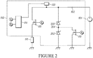
Figure 2 is an electrical schematic diagram of the electrical system according to an exemplary embodiment with the plurality of voltage suppressors arranged generally in series; and -
Figure 3 is a flowchart showing a method of operating the electrical system according to one exemplary embodiment. - Referring to the Figures, wherein like numerals indicate like parts throughout the several views, an
electrical system 100 is shown and described herein. - In one exemplary embodiment, the
electrical system 100 may be implemented as part of a vehicle (not shown), e.g., an automobile (not shown). More particularly, theelectrical system 100 may be implemented as part of an engine control module (not shown) of the vehicle. However, it should be appreciated that theelectrical system 100 may be implemented in numerous other applications other than the engine control module and/or the vehicle. - Some or all of the components of the
electrical system 100 described herein may be supported by one or more circuit boards (not shown). As appreciated by those skilled in the art, the circuit board may provide electrical connections via conductive traces between the various components. - The
electrical system 100 includes aninput node 102. Theinput node 102 is electrically connectable to apower supply 104. In the exemplary embodiment, thepower supply 104 provides direct current ("DC") power, which is received at theinput node 102. Thepower supply 104 may provide DC power at one or more voltage levels. For instance, in one exemplary embodiment, thepower supply 104 provides DC power at 12 volts ("V"). In another exemplary embodiment, thepower supply 104 provides DC power at 24 V. Of course, the DC power supplied by thepower supply 104 may be at any appropriate voltage level. Thepower supply 104 may be include a battery (not separately shown), a capacitor (not separately shown), and/or a solar cell (not separately shown). Of course, those skilled in the art will appreciate other devices and/or techniques to implement thepower supply 104. - The
electrical system 100 further includes a plurality ofvoltage suppressors voltage suppressors transient voltage suppressors transient voltage suppressors electrical system 100. Thetransient voltage suppressors - In the exemplary embodiments, at least one of the plurality of
voltage suppressors input node 102. In the embodiment shown inFigure 1 , a first transient voltage suppressor 106 and a second transient voltage suppressor 108 are each electrically connected to theinput node 102. More particularly, a cathode (not numbered) of each transient voltage suppressor 106, 108 is electrically connected to theinput node 102. - The
electrical system 100 also includes avoltage selection switch 110 electrically connected to at least one of the plurality ofvoltage suppressors Figure 1 , thevoltage selection switch 110 is electrically connected to the first transient voltage suppressor 106. More particularly, thevoltage selection switch 110 is electrically connected between an anode (not numbered) of the first transient voltage suppressor 106 and aground 112. - In the exemplary embodiment shown in
Figure 1 , thevoltage selection switch 110 is implemented a transistor (not separately numbered), and more specifically a metal-oxide-semiconductor field-effect transistor ("MOSFET") (not separately numbered). However, it should be appreciated that other devices may be utilized to implement thevoltage selection switch 110. - As can be seen in
Figure 1 , the second voltage suppressor 108 is always in electrical connection between theinput node 102 and theground 112, while the first voltage suppressor 108 is only in electrical connection between theinput node 102 and the ground when thevoltage selection switch 110 is active, i.e., "closed". - In the embodiment shown in
Figure 1 , the first voltage suppressor 106 exhibits a first clamping voltage. More specifically, in this exemplary embodiment, the first voltage suppressor 106 has a clamping voltage, i.e., a standoff voltage, of about 26 V. The second voltage suppressor 108 exhibits a second clamping voltage less than the first clamping voltage. More specifically, in this embodiment, the second voltage suppressor 108 has a clamping voltage of about 43 V. - The
electrical system 100 further includes acontroller 114. Thecontroller 114 may utilize a microprocessor, microcontroller, application specific integrated circuit ("ASIC"), and/or other device for controlling operation of theelectrical system 100, performing calculations, and/or executing instructions (i.e., running a program). Thecontroller 114 may also utilize a memory (not shown) for storing instructions and/or data. The memory may be implemented with transistors, a hard disk, an optical disk, and/or any other suitable storage device as appreciated by those skilled in the art. - The
controller 114 is in communication with thevoltage selection switch 110 to selectively operate theswitch 110 based on a nominal operating voltage of thepower supply 104 and/or at theinput node 102. As on example, as shown in the embodiment ofFigure 1 , when thepower supply 104 voltage is 12 V, thevoltage selection switch 110 is activated, i.e., closed, by thecontroller 114. As such, the first transient voltage suppressor 106 clamps the input voltage to 26 V. When thepower supply 104 voltage is 24 V, thevoltage selection switch 110 is deactivated, i.e., opened. Accordingly, the first transient voltage suppressor 106 is disconnected, so the second transient voltage suppressor 108 clamps the input voltage to 43 V. - In another exemplary embodiment, as shown in
Figure 2 , the plurality ofvoltage suppressors first voltage suppressor 200 and asecond voltage suppressor 202 electrically connected in series between theinput node 102 andground 112. In this embodiment, thevoltage selection switch 110 is electrically connected between theground 112 and anode 204 between thevoltage suppressors - In this exemplary embodiment, the
first voltage suppressor 200 exhibits a clamping voltage of about 22 V while thesecond voltage suppressor 202 exhibits a clamping voltage of about 20 V. More particularly, in this exemplary embodiment thefirst voltage suppressor 200 is implemented with a model No. SM8S22A and thesecond voltage suppressor 202 is implemented with a model No. SM8S20A, both manufactured by Vishay Intertechnology, Inc. of Shelton, Connecticut. Of course, in other embodiments, thevoltage suppressors - In the embodiment shown in
Figure 2 , the first andsecond voltage suppressors input node 102 and theground 112. As such, when thevoltage selection switch 110 is deactivated, i.e., open, thevoltage suppressors input node 102 and theground 112. However, when thevoltage selection switch 110 is activated, i.e., closed, the clamping voltage between theinput node 102 and theground 112 becomes about 22 V, as thesecond voltage suppressor 202 is bypassed. - Referring now to
Figures 1 or2 , at least oneload 116 may be electrically connectable to theinput node 102. Theelectrical system 100 may include at least oneload operation switch 118 electrically connected to the at least oneload 116 for selectively electrifying the at least oneload 116. Oneload operation switch 118 is shown in each of the figures, implemented as a MOSFET (not separately numbered). Theload operation switch 118 may be referred to as a "driver" by those skilled in the art. When disposed between theinput node 102 and theload 116, theload operation switch 118 may be referred to as a "high-side driver" by those skilled in the art. Of course, other techniques and devices for implementing theload operation switch 118 may be utilized. - The
load 116 may be available from its manufacturer in different versions which require different operating voltages. For example, a manufacturer may supply aload 116 in a 12 V version and a 24 V version. Each of these versions have different voltage suppression needs. Thesystem 100, as further described herein, is configured to provide the different voltage suppression needs for either version of theload 116. - The
electrical system 100 may further include asensor 120. Thesensor 120 is electrically connected to theinput node 102 and configured to sense a nominal operating voltage at theinput node 102. For example, thesensor 120 may detect whether the nominal operating voltage, i.e., the voltage of thepower supply 104 is 12 V or 24 V. Thesensor 120 may be in communication with thecontroller 114, such that the sensed voltage is communicated to thecontroller 114. Thecontroller 114 may then utilize this sensed voltage to determine whether or not to activate thevoltage selection switch 110. However, it should be appreciated that theelectrical system 100 may be implemented without thesensor 120. For instance, software running in thecontroller 114 may be programmed at manufacturing or at the point of sale to operate thevoltage selection switch 110 based on the installation into a 12 V or 24 V electrical system. - Referring now to
Figure 3 , amethod 300 of operating anelectrical system 100 is also disclosed. While theexemplary method 300 describes operation of theelectrical system 100 shown inFigures 1 and2 and as described above, it should be appreciated that themethod 300 may be utilized on other systems and devices (not shown). Of course, themethod 300 may be operated by thecontroller 114 and/or other processing devices (not shown). - The
method 300 includes, at 302, determining a voltage at aninput node 102. Determining the voltage at theinput node 102 may be accomplished, as described above, by utilizing asensor 120 and/or by querying the memory in thecontroller 114. Themethod 300 further includes, at 304, selectively operating avoltage selection switch 110 electrically connected to at least one of a plurality ofvoltage suppressors - The
method 300 also may include, at 306, selectively operating aload operation switch 118 after operation of thevoltage selection switch 110. As such, electrical power is not transmitted to theload 116 until after theappropriate voltage suppressors voltage selection switch 110. - The present invention has been described herein in an illustrative manner, and it is to be understood that the terminology which has been used is intended to be in the nature of words of description rather than of limitation. Obviously, many modifications and variations of the invention are possible in light of the appended claims. The invention may be practiced otherwise than as specifically described within the scope of the appended claims.
Claims (10)
- An electrical system (100) comprising:an input node (102) electrically connectable to a power supply (104);a plurality of voltage suppressors (106, 108);a voltage selection switch (110) electrically connected to at least one of said plurality of voltage suppressors (106, 108) and a ground (112); anda controller (114) in communication with said switch (110) configured to selectively operate said switch (110) based on a nominal operating voltage at said input node (102).wherein said plurality of voltage suppressors (106, 108) comprises a first voltage suppressor (108) electrically connected between said input node (102) and ground (112) and a second voltage suppressor (106) electrically connected between said input node (102) and said voltage selection switch (110),characterized inthat said first voltage suppressor (108) exhibits a first clamping voltage and said second voltage suppressor (106) exhibits a second clamping voltage less than the first clamping voltage.
- An electrical system (100) comprising:an input node (102) electrically connectable to a power supply (104);a plurality of voltage suppressors (200, 202);a voltage selection switch (110) electrically connected to at least one of said plurality of voltage suppressors (200, 202) and a ground (112); anda controller (114) in communication with said switch (110) configured to selectively operate said switch (110) based on a nominal operating voltage at said input node (102).characterized inthat said plurality of voltage suppressors (200, 202) comprises a first voltage suppressor (200) and a second voltage suppressor (202) electrically connected in series between said input node (102) and a ground (112) and wherein said voltage selection switch (110) is electrically connected between said ground (112) and a node (204) between said voltage suppressors (200, 202).
- The system (100) as set forth in claim 2 wherein said first voltage suppressor (200) and said second voltage suppressor (202) each exhibit a first clamping voltage.
- The system (100) as set forth in claim 1 or 2 further comprising a sensor (120) electrically connected to said input node (102) configured for sensing a nominal operating voltage at said input node (102).
- The system (100) as set forth in claim 4 wherein said controller (114) is in communication with said sensor (120) configured for receiving the nominal operating voltage sensed by said sensor (120).
- The system (100) as set forth in claim 1 further comprising at least one load (116) electrically connectable to said input node (102).
- The system (100) as set forth in claim 6 further comprising at least one load operation switch (118) electrically connected between said input node (102) and said at least one load (116) configured for selectively electrifying said at least one load (116).
- The system (100) as set forth in claim 7 wherein said at least one load operation switch (118) is a transistor electrically connected between said input node (102) and said at least one load (116).
- The system (100) as set forth in claim 1 or 2 wherein at least one of said plurality of voltage suppressors (106. 108; 200, 202) is a diode.
- The system (100) as set forth in claim 1 or 2 wherein said input node (102) is configured to receive a direct current (DC) input from the power supply (104).
Applications Claiming Priority (2)
| Application Number | Priority Date | Filing Date | Title |
|---|---|---|---|
| US15/140,959 US10277028B2 (en) | 2016-04-28 | 2016-04-28 | Selectable input transient voltage suppressor |
| PCT/US2017/028616 WO2017189331A1 (en) | 2016-04-28 | 2017-04-20 | Selectable input transient voltage suppressor |
Publications (2)
| Publication Number | Publication Date |
|---|---|
| EP3449542A1 EP3449542A1 (en) | 2019-03-06 |
| EP3449542B1 true EP3449542B1 (en) | 2022-07-27 |
Family
ID=58701852
Family Applications (1)
| Application Number | Title | Priority Date | Filing Date |
|---|---|---|---|
| EP17723184.2A Active EP3449542B1 (en) | 2016-04-28 | 2017-04-20 | Selectable input transient voltage suppressor |
Country Status (5)
| Country | Link |
|---|---|
| US (2) | US10277028B2 (en) |
| EP (1) | EP3449542B1 (en) |
| KR (1) | KR102206688B1 (en) |
| CN (1) | CN109075568B (en) |
| WO (1) | WO2017189331A1 (en) |
Cited By (1)
| Publication number | Priority date | Publication date | Assignee | Title |
|---|---|---|---|---|
| US12253552B2 (en) | 2021-10-01 | 2025-03-18 | Faraday Defense Corporation | Apparatus for detection of electrical disturbances resulting from electromagnetic pulse |
Family Cites Families (12)
| Publication number | Priority date | Publication date | Assignee | Title |
|---|---|---|---|---|
| DE4029794A1 (en) * | 1990-08-18 | 1992-02-20 | Bosch Gmbh Robert | METHOD AND DEVICE FOR CONTROLLING AN ELECTROMAGNETIC CONSUMER |
| DE10135168A1 (en) * | 2001-07-19 | 2003-02-13 | Bosch Gmbh Robert | Device for protecting electronic components |
| US8179653B2 (en) | 2008-07-17 | 2012-05-15 | Advanced Protection Technologies, Inc. | Multiple operating voltage electrical surge protection apparatus |
| DE102008041099A1 (en) | 2008-08-07 | 2010-02-11 | Robert Bosch Gmbh | Method for protecting electronic component against over voltage of supply voltage of electrical system of motor vehicle, involves activating transistor and diode to limit voltage, and deactivating transistor and diode after preset interval |
| DE102009041329A1 (en) * | 2009-09-15 | 2011-03-24 | Celon Ag Medical Instruments | Combined Ultrasonic and HF Surgical System |
| US20110279940A1 (en) * | 2010-05-12 | 2011-11-17 | Jian Xu | System and method for providing overvoltage protection |
| US8929042B2 (en) * | 2011-03-30 | 2015-01-06 | Thomas & Betts International, Inc. | Surge protective device with contoller |
| WO2013160723A1 (en) | 2012-04-23 | 2013-10-31 | Freescale Semiconductor, Inc. | A semiconductor device arrangement, a method of analysing a performance of a functional circuit on a semiconductor device and a device analysis system |
| US9018931B2 (en) * | 2012-12-19 | 2015-04-28 | Solidstate Controls, Llc | Control system for providing circuit protection to a power supply |
| JP6052149B2 (en) | 2013-12-06 | 2016-12-27 | ソニー株式会社 | Power receiving device, power receiving control method, non-contact power feeding system, and electronic device |
| US9671453B2 (en) * | 2014-10-01 | 2017-06-06 | Hamilton Sundstrand Corporation | Built in test circuit for transient voltage suppressor devices |
| US10511163B2 (en) * | 2015-12-29 | 2019-12-17 | General Electric Company | Low capacitance surge suppression device |
-
2016
- 2016-04-28 US US15/140,959 patent/US10277028B2/en active Active
-
2017
- 2017-04-20 CN CN201780026094.1A patent/CN109075568B/en active Active
- 2017-04-20 KR KR1020187030690A patent/KR102206688B1/en active Active
- 2017-04-20 WO PCT/US2017/028616 patent/WO2017189331A1/en not_active Ceased
- 2017-04-20 EP EP17723184.2A patent/EP3449542B1/en active Active
-
2019
- 2019-04-29 US US16/398,111 patent/US10742024B2/en active Active
Cited By (1)
| Publication number | Priority date | Publication date | Assignee | Title |
|---|---|---|---|---|
| US12253552B2 (en) | 2021-10-01 | 2025-03-18 | Faraday Defense Corporation | Apparatus for detection of electrical disturbances resulting from electromagnetic pulse |
Also Published As
| Publication number | Publication date |
|---|---|
| KR20180126041A (en) | 2018-11-26 |
| KR102206688B1 (en) | 2021-01-22 |
| US10277028B2 (en) | 2019-04-30 |
| WO2017189331A1 (en) | 2017-11-02 |
| US10742024B2 (en) | 2020-08-11 |
| US20170315575A1 (en) | 2017-11-02 |
| EP3449542A1 (en) | 2019-03-06 |
| CN109075568B (en) | 2020-06-09 |
| US20190252876A1 (en) | 2019-08-15 |
| CN109075568A (en) | 2018-12-21 |
Similar Documents
| Publication | Publication Date | Title |
|---|---|---|
| US12224738B2 (en) | Switch device | |
| US10306725B2 (en) | Light source drive device and vehicle lamp | |
| US10340908B2 (en) | Half-bridge driver fault diagnostic system and method | |
| US9600047B2 (en) | Electronic control unit | |
| US6249110B1 (en) | Circuit configuration for generating a stabilized power supply voltage | |
| CN104044541B (en) | Airbag apparatus | |
| EP3190680B1 (en) | Battery protection circuit | |
| JP6466025B2 (en) | Control circuit | |
| JP2010110091A (en) | Load driving device | |
| US20230223746A1 (en) | Clamper, input circuit, and semiconductor device | |
| US10088882B2 (en) | Electronic control unit having multiple power supply routes for microcomputer core | |
| US10742024B2 (en) | Selectable input transient voltage suppressor | |
| US20150092312A1 (en) | Circuit for protecting an electronic control unit (ecu) from high energy pulses | |
| US10179560B2 (en) | Method and device for disconnecting at least one ignition output stage for a squib of a pyrotechnic protection means for a vehicle | |
| CN101855605B (en) | System and method for preserving processor memory during power loss | |
| US20090206656A1 (en) | Personal Protection Control Unit | |
| US10523044B2 (en) | Device for controlling the electrical power supply of a circuit for a vehicle, comprising a battery and corresponding assembly | |
| JP2015149531A (en) | Circuit device and power supply system | |
| JP2018058543A (en) | On-vehicle equipment | |
| US10641785B2 (en) | Wheel speed sensor | |
| WO2021124719A1 (en) | In-vehicle semiconductor circuit and semiconductor circuit | |
| JP2008148380A (en) | Overvoltage protection circuit | |
| EP4477478A1 (en) | Crash switch circuit and crash detection system including the same | |
| US20180309434A1 (en) | Semiconductor device and control device | |
| EP3836328B1 (en) | Reverse voltage protection |
Legal Events
| Date | Code | Title | Description |
|---|---|---|---|
| STAA | Information on the status of an ep patent application or granted ep patent |
Free format text: STATUS: UNKNOWN |
|
| STAA | Information on the status of an ep patent application or granted ep patent |
Free format text: STATUS: THE INTERNATIONAL PUBLICATION HAS BEEN MADE |
|
| PUAI | Public reference made under article 153(3) epc to a published international application that has entered the european phase |
Free format text: ORIGINAL CODE: 0009012 |
|
| STAA | Information on the status of an ep patent application or granted ep patent |
Free format text: STATUS: REQUEST FOR EXAMINATION WAS MADE |
|
| 17P | Request for examination filed |
Effective date: 20181128 |
|
| AK | Designated contracting states |
Kind code of ref document: A1 Designated state(s): AL AT BE BG CH CY CZ DE DK EE ES FI FR GB GR HR HU IE IS IT LI LT LU LV MC MK MT NL NO PL PT RO RS SE SI SK SM TR |
|
| AX | Request for extension of the european patent |
Extension state: BA ME |
|
| DAV | Request for validation of the european patent (deleted) | ||
| DAX | Request for extension of the european patent (deleted) | ||
| STAA | Information on the status of an ep patent application or granted ep patent |
Free format text: STATUS: EXAMINATION IS IN PROGRESS |
|
| 17Q | First examination report despatched |
Effective date: 20200528 |
|
| RAP1 | Party data changed (applicant data changed or rights of an application transferred) |
Owner name: CONTINENTAL AUTOMOTIVE SYSTEMS, INC. |
|
| GRAP | Despatch of communication of intention to grant a patent |
Free format text: ORIGINAL CODE: EPIDOSNIGR1 |
|
| STAA | Information on the status of an ep patent application or granted ep patent |
Free format text: STATUS: GRANT OF PATENT IS INTENDED |
|
| INTG | Intention to grant announced |
Effective date: 20220223 |
|
| GRAS | Grant fee paid |
Free format text: ORIGINAL CODE: EPIDOSNIGR3 |
|
| GRAA | (expected) grant |
Free format text: ORIGINAL CODE: 0009210 |
|
| STAA | Information on the status of an ep patent application or granted ep patent |
Free format text: STATUS: THE PATENT HAS BEEN GRANTED |
|
| AK | Designated contracting states |
Kind code of ref document: B1 Designated state(s): AL AT BE BG CH CY CZ DE DK EE ES FI FR GB GR HR HU IE IS IT LI LT LU LV MC MK MT NL NO PL PT RO RS SE SI SK SM TR |
|
| REG | Reference to a national code |
Ref country code: CH Ref legal event code: EP |
|
| REG | Reference to a national code |
Ref country code: AT Ref legal event code: REF Ref document number: 1507726 Country of ref document: AT Kind code of ref document: T Effective date: 20220815 |
|
| REG | Reference to a national code |
Ref country code: DE Ref legal event code: R096 Ref document number: 602017059866 Country of ref document: DE |
|
| REG | Reference to a national code |
Ref country code: IE Ref legal event code: FG4D |
|
| REG | Reference to a national code |
Ref country code: LT Ref legal event code: MG9D |
|
| REG | Reference to a national code |
Ref country code: NL Ref legal event code: MP Effective date: 20220727 |
|
| PG25 | Lapsed in a contracting state [announced via postgrant information from national office to epo] |
Ref country code: SE Free format text: LAPSE BECAUSE OF FAILURE TO SUBMIT A TRANSLATION OF THE DESCRIPTION OR TO PAY THE FEE WITHIN THE PRESCRIBED TIME-LIMIT Effective date: 20220727 Ref country code: RS Free format text: LAPSE BECAUSE OF FAILURE TO SUBMIT A TRANSLATION OF THE DESCRIPTION OR TO PAY THE FEE WITHIN THE PRESCRIBED TIME-LIMIT Effective date: 20220727 Ref country code: PT Free format text: LAPSE BECAUSE OF FAILURE TO SUBMIT A TRANSLATION OF THE DESCRIPTION OR TO PAY THE FEE WITHIN THE PRESCRIBED TIME-LIMIT Effective date: 20221128 Ref country code: NO Free format text: LAPSE BECAUSE OF FAILURE TO SUBMIT A TRANSLATION OF THE DESCRIPTION OR TO PAY THE FEE WITHIN THE PRESCRIBED TIME-LIMIT Effective date: 20221027 Ref country code: NL Free format text: LAPSE BECAUSE OF FAILURE TO SUBMIT A TRANSLATION OF THE DESCRIPTION OR TO PAY THE FEE WITHIN THE PRESCRIBED TIME-LIMIT Effective date: 20220727 Ref country code: LV Free format text: LAPSE BECAUSE OF FAILURE TO SUBMIT A TRANSLATION OF THE DESCRIPTION OR TO PAY THE FEE WITHIN THE PRESCRIBED TIME-LIMIT Effective date: 20220727 Ref country code: LT Free format text: LAPSE BECAUSE OF FAILURE TO SUBMIT A TRANSLATION OF THE DESCRIPTION OR TO PAY THE FEE WITHIN THE PRESCRIBED TIME-LIMIT Effective date: 20220727 Ref country code: FI Free format text: LAPSE BECAUSE OF FAILURE TO SUBMIT A TRANSLATION OF THE DESCRIPTION OR TO PAY THE FEE WITHIN THE PRESCRIBED TIME-LIMIT Effective date: 20220727 Ref country code: ES Free format text: LAPSE BECAUSE OF FAILURE TO SUBMIT A TRANSLATION OF THE DESCRIPTION OR TO PAY THE FEE WITHIN THE PRESCRIBED TIME-LIMIT Effective date: 20220727 |
|
| REG | Reference to a national code |
Ref country code: AT Ref legal event code: MK05 Ref document number: 1507726 Country of ref document: AT Kind code of ref document: T Effective date: 20220727 |
|
| PG25 | Lapsed in a contracting state [announced via postgrant information from national office to epo] |
Ref country code: PL Free format text: LAPSE BECAUSE OF FAILURE TO SUBMIT A TRANSLATION OF THE DESCRIPTION OR TO PAY THE FEE WITHIN THE PRESCRIBED TIME-LIMIT Effective date: 20220727 Ref country code: IS Free format text: LAPSE BECAUSE OF FAILURE TO SUBMIT A TRANSLATION OF THE DESCRIPTION OR TO PAY THE FEE WITHIN THE PRESCRIBED TIME-LIMIT Effective date: 20221127 Ref country code: HR Free format text: LAPSE BECAUSE OF FAILURE TO SUBMIT A TRANSLATION OF THE DESCRIPTION OR TO PAY THE FEE WITHIN THE PRESCRIBED TIME-LIMIT Effective date: 20220727 Ref country code: GR Free format text: LAPSE BECAUSE OF FAILURE TO SUBMIT A TRANSLATION OF THE DESCRIPTION OR TO PAY THE FEE WITHIN THE PRESCRIBED TIME-LIMIT Effective date: 20221028 |
|
| PG25 | Lapsed in a contracting state [announced via postgrant information from national office to epo] |
Ref country code: SM Free format text: LAPSE BECAUSE OF FAILURE TO SUBMIT A TRANSLATION OF THE DESCRIPTION OR TO PAY THE FEE WITHIN THE PRESCRIBED TIME-LIMIT Effective date: 20220727 Ref country code: RO Free format text: LAPSE BECAUSE OF FAILURE TO SUBMIT A TRANSLATION OF THE DESCRIPTION OR TO PAY THE FEE WITHIN THE PRESCRIBED TIME-LIMIT Effective date: 20220727 Ref country code: DK Free format text: LAPSE BECAUSE OF FAILURE TO SUBMIT A TRANSLATION OF THE DESCRIPTION OR TO PAY THE FEE WITHIN THE PRESCRIBED TIME-LIMIT Effective date: 20220727 Ref country code: CZ Free format text: LAPSE BECAUSE OF FAILURE TO SUBMIT A TRANSLATION OF THE DESCRIPTION OR TO PAY THE FEE WITHIN THE PRESCRIBED TIME-LIMIT Effective date: 20220727 Ref country code: AT Free format text: LAPSE BECAUSE OF FAILURE TO SUBMIT A TRANSLATION OF THE DESCRIPTION OR TO PAY THE FEE WITHIN THE PRESCRIBED TIME-LIMIT Effective date: 20220727 |
|
| REG | Reference to a national code |
Ref country code: DE Ref legal event code: R097 Ref document number: 602017059866 Country of ref document: DE |
|
| PG25 | Lapsed in a contracting state [announced via postgrant information from national office to epo] |
Ref country code: SK Free format text: LAPSE BECAUSE OF FAILURE TO SUBMIT A TRANSLATION OF THE DESCRIPTION OR TO PAY THE FEE WITHIN THE PRESCRIBED TIME-LIMIT Effective date: 20220727 Ref country code: EE Free format text: LAPSE BECAUSE OF FAILURE TO SUBMIT A TRANSLATION OF THE DESCRIPTION OR TO PAY THE FEE WITHIN THE PRESCRIBED TIME-LIMIT Effective date: 20220727 |
|
| PLBE | No opposition filed within time limit |
Free format text: ORIGINAL CODE: 0009261 |
|
| STAA | Information on the status of an ep patent application or granted ep patent |
Free format text: STATUS: NO OPPOSITION FILED WITHIN TIME LIMIT |
|
| PG25 | Lapsed in a contracting state [announced via postgrant information from national office to epo] |
Ref country code: AL Free format text: LAPSE BECAUSE OF FAILURE TO SUBMIT A TRANSLATION OF THE DESCRIPTION OR TO PAY THE FEE WITHIN THE PRESCRIBED TIME-LIMIT Effective date: 20220727 |
|
| 26N | No opposition filed |
Effective date: 20230502 |
|
| PG25 | Lapsed in a contracting state [announced via postgrant information from national office to epo] |
Ref country code: SI Free format text: LAPSE BECAUSE OF FAILURE TO SUBMIT A TRANSLATION OF THE DESCRIPTION OR TO PAY THE FEE WITHIN THE PRESCRIBED TIME-LIMIT Effective date: 20220727 |
|
| REG | Reference to a national code |
Ref country code: CH Ref legal event code: PL |
|
| GBPC | Gb: european patent ceased through non-payment of renewal fee |
Effective date: 20230420 |
|
| PG25 | Lapsed in a contracting state [announced via postgrant information from national office to epo] |
Ref country code: LU Free format text: LAPSE BECAUSE OF NON-PAYMENT OF DUE FEES Effective date: 20230420 |
|
| REG | Reference to a national code |
Ref country code: BE Ref legal event code: MM Effective date: 20230430 |
|
| PG25 | Lapsed in a contracting state [announced via postgrant information from national office to epo] |
Ref country code: MC Free format text: LAPSE BECAUSE OF FAILURE TO SUBMIT A TRANSLATION OF THE DESCRIPTION OR TO PAY THE FEE WITHIN THE PRESCRIBED TIME-LIMIT Effective date: 20220727 |
|
| PG25 | Lapsed in a contracting state [announced via postgrant information from national office to epo] |
Ref country code: GB Free format text: LAPSE BECAUSE OF NON-PAYMENT OF DUE FEES Effective date: 20230420 |
|
| PG25 | Lapsed in a contracting state [announced via postgrant information from national office to epo] |
Ref country code: MC Free format text: LAPSE BECAUSE OF FAILURE TO SUBMIT A TRANSLATION OF THE DESCRIPTION OR TO PAY THE FEE WITHIN THE PRESCRIBED TIME-LIMIT Effective date: 20220727 Ref country code: LI Free format text: LAPSE BECAUSE OF NON-PAYMENT OF DUE FEES Effective date: 20230430 Ref country code: GB Free format text: LAPSE BECAUSE OF NON-PAYMENT OF DUE FEES Effective date: 20230420 Ref country code: CH Free format text: LAPSE BECAUSE OF NON-PAYMENT OF DUE FEES Effective date: 20230430 |
|
| REG | Reference to a national code |
Ref country code: IE Ref legal event code: MM4A |
|
| PG25 | Lapsed in a contracting state [announced via postgrant information from national office to epo] |
Ref country code: BE Free format text: LAPSE BECAUSE OF NON-PAYMENT OF DUE FEES Effective date: 20230430 |
|
| PG25 | Lapsed in a contracting state [announced via postgrant information from national office to epo] |
Ref country code: IE Free format text: LAPSE BECAUSE OF NON-PAYMENT OF DUE FEES Effective date: 20230420 |
|
| PG25 | Lapsed in a contracting state [announced via postgrant information from national office to epo] |
Ref country code: IE Free format text: LAPSE BECAUSE OF NON-PAYMENT OF DUE FEES Effective date: 20230420 |
|
| PG25 | Lapsed in a contracting state [announced via postgrant information from national office to epo] |
Ref country code: IT Free format text: LAPSE BECAUSE OF FAILURE TO SUBMIT A TRANSLATION OF THE DESCRIPTION OR TO PAY THE FEE WITHIN THE PRESCRIBED TIME-LIMIT Effective date: 20220727 |
|
| PG25 | Lapsed in a contracting state [announced via postgrant information from national office to epo] |
Ref country code: BG Free format text: LAPSE BECAUSE OF FAILURE TO SUBMIT A TRANSLATION OF THE DESCRIPTION OR TO PAY THE FEE WITHIN THE PRESCRIBED TIME-LIMIT Effective date: 20220727 |
|
| PG25 | Lapsed in a contracting state [announced via postgrant information from national office to epo] |
Ref country code: BG Free format text: LAPSE BECAUSE OF FAILURE TO SUBMIT A TRANSLATION OF THE DESCRIPTION OR TO PAY THE FEE WITHIN THE PRESCRIBED TIME-LIMIT Effective date: 20220727 |
|
| PGFP | Annual fee paid to national office [announced via postgrant information from national office to epo] |
Ref country code: DE Payment date: 20250430 Year of fee payment: 9 |
|
| PGFP | Annual fee paid to national office [announced via postgrant information from national office to epo] |
Ref country code: FR Payment date: 20250425 Year of fee payment: 9 |
|
| PG25 | Lapsed in a contracting state [announced via postgrant information from national office to epo] |
Ref country code: CY Free format text: LAPSE BECAUSE OF FAILURE TO SUBMIT A TRANSLATION OF THE DESCRIPTION OR TO PAY THE FEE WITHIN THE PRESCRIBED TIME-LIMIT; INVALID AB INITIO Effective date: 20170420 |
|
| PG25 | Lapsed in a contracting state [announced via postgrant information from national office to epo] |
Ref country code: HU Free format text: LAPSE BECAUSE OF FAILURE TO SUBMIT A TRANSLATION OF THE DESCRIPTION OR TO PAY THE FEE WITHIN THE PRESCRIBED TIME-LIMIT; INVALID AB INITIO Effective date: 20170420 |
|
| PG25 | Lapsed in a contracting state [announced via postgrant information from national office to epo] |
Ref country code: TR Free format text: LAPSE BECAUSE OF FAILURE TO SUBMIT A TRANSLATION OF THE DESCRIPTION OR TO PAY THE FEE WITHIN THE PRESCRIBED TIME-LIMIT Effective date: 20220727 |