EP3447939A1 - Carrier frequency estimation method and associated processing unit, detection method and associated receiver - Google Patents
Carrier frequency estimation method and associated processing unit, detection method and associated receiver Download PDFInfo
- Publication number
- EP3447939A1 EP3447939A1 EP17306092.2A EP17306092A EP3447939A1 EP 3447939 A1 EP3447939 A1 EP 3447939A1 EP 17306092 A EP17306092 A EP 17306092A EP 3447939 A1 EP3447939 A1 EP 3447939A1
- Authority
- EP
- European Patent Office
- Prior art keywords
- phase
- signal
- amplitude
- modulation
- states
- Prior art date
- Legal status (The legal status is an assumption and is not a legal conclusion. Google has not performed a legal analysis and makes no representation as to the accuracy of the status listed.)
- Withdrawn
Links
- 238000000034 method Methods 0.000 title claims abstract description 24
- 238000001514 detection method Methods 0.000 title description 3
- 230000003287 optical effect Effects 0.000 claims abstract description 26
- 230000000694 effects Effects 0.000 claims abstract description 6
- 230000010287 polarization Effects 0.000 claims description 11
- 230000001427 coherent effect Effects 0.000 claims description 8
- 238000011084 recovery Methods 0.000 claims description 8
- 238000007493 shaping process Methods 0.000 claims description 6
- 238000012952 Resampling Methods 0.000 claims description 5
- 238000006243 chemical reaction Methods 0.000 claims description 5
- 239000006185 dispersion Substances 0.000 claims description 5
- 230000014509 gene expression Effects 0.000 claims description 5
- 238000001914 filtration Methods 0.000 claims description 3
- 230000006870 function Effects 0.000 description 16
- 238000010586 diagram Methods 0.000 description 7
- 230000005540 biological transmission Effects 0.000 description 4
- 239000013307 optical fiber Substances 0.000 description 2
- 230000010363 phase shift Effects 0.000 description 2
- 238000012935 Averaging Methods 0.000 description 1
- 239000000654 additive Substances 0.000 description 1
- 230000000996 additive effect Effects 0.000 description 1
- 238000004364 calculation method Methods 0.000 description 1
- 230000001419 dependent effect Effects 0.000 description 1
- 230000003993 interaction Effects 0.000 description 1
- 230000003595 spectral effect Effects 0.000 description 1
Images



Classifications
-
- H—ELECTRICITY
- H04—ELECTRIC COMMUNICATION TECHNIQUE
- H04B—TRANSMISSION
- H04B10/00—Transmission systems employing electromagnetic waves other than radio-waves, e.g. infrared, visible or ultraviolet light, or employing corpuscular radiation, e.g. quantum communication
- H04B10/60—Receivers
- H04B10/61—Coherent receivers
- H04B10/616—Details of the electronic signal processing in coherent optical receivers
- H04B10/6164—Estimation or correction of the frequency offset between the received optical signal and the optical local oscillator
Definitions
- the present invention refers to the reception of an optical signal and more specifically to the carrier frequency estimation of an optical signal modulated in amplitude and phase.
- Fig.1a represents the constellation symbols in the case of a Quadrature Phase Shift Keying (QPSK) and Fig.1b represents the results of the application of a fourth power to the constellation symbols of Fig.1a . Only the real and positive part of the constellation symbols remains.
- QPSK Quadrature Phase Shift Keying
- the frequency offset can be retrieved using the following frequency estimator:
- the invention refers to a method for estimating a carrier frequency offset at the reception of an optical signal modulated in amplitude and phase, the signal comprising a series of modulation symbols, the method comprising the following steps:
- the modulation format corresponds to a modulation format based on constellation shaping.
- the function f is computed for N equally spaced frequencies by a fast fourier transform "FFT" of the corrected states.
- the predetermined correction factor is a sign correction factor for the M th power resulting states located in the left hemisphere of the complex plane in the absence of phase and frequency shift.
- the sign correction factor depends on the amplitude of the modulation symbols.
- the predetermined correction factor is a weighted factor based on a calculated variance of an estimated phase of the different M th power resulting states.
- the variance of the estimated phase of the different Mth power resulting states depends on their amplitude.
- the modulation format corresponds to a square quadrature amplitude modulation "QAM" format and wherein the number M of the power is equal to four.
- the method comprises the following preliminary steps:
- the present invention also refers to a method for detecting a received optical signal modulated in amplitude and phase wherein the method comprises the following steps:
- the present invention also refers to a processing unit configured for estimating a carrier frequency of a received optical signal modulated in amplitude and phase, the signal comprising a series of modulation symbols and the processing unit being configured for:
- the present invention also refers to an optical receiver comprising:
- Fig.3 discloses the structure of an optical receiver 1 based on a coherent detection.
- the optical receiver 1 comprises a local oscillator 3, generally a tunable laser source and a coherent mixer 5.
- the coherent mixer 5 comprises a first input 5a linked to the input 1a of the optical receiver 1 which is generally connected to an optical transmission mean such as an optical fiber 7 and a second input 5b linked to the local oscillator 3.
- the local oscillator 3 is set at the same frequency as the signal received on the input 1a in order to enable the detection of the said received signal.
- the coherent mixer 5 is configured for mixing the incoming signal received from the optical fiber 7 and the signal produced by the local oscillator 3.
- the optical receiver 1 also comprises a plurality (four in the present case) of optical detectors 9 such as photo-diodes configured for detecting the different parts (in-phase and quadrature parts of the different polarizations) of the mixed signal.
- the optical receiver 1 also comprises a plurality of analog to digital conversion units 11 configured to convert the signals detected by the optical detectors 9 into digital signals in order to apply digital signal processing on these signals.
- the optical receiver 1 also comprises a digital processing unit 13.
- the digital processing unit 13 refers for example to a processor.
- Fig.4a represents the different steps of the digital signal processing.
- the first step 101 refers to a deskew and resampling step.
- the second step 102 refers to a chromatic dispersion step.
- the third step 103 refers to a timing recovery step wherein the modulation frequency is recovered.
- the fourth step 104 refers to a polarization demultipexing step.
- Such polarization demultiplexing is for example achieved by a constant modulus algorithm.
- the fifth step 105 refers to a frequency offset recovery configured for estimating the data signal frequency of the transmitted signal and for compensating the frequency detuning between the incoming signal frequency and the local oscillator frequency.
- the sixth step 106 refers to a carrier phase recovery wherein the phase noise is filtered in order to retrieve the carrier phase.
- the seventh step 107 refers to a demapping step wherein the constellation symbols are converted into data bits.
- the present invention deals more specifically with the fifth step 105 and the frequency offset recovery when the incoming signal is modulated in amplitude and phase, for example when quadrature phase shift keying (QPSK) or quadrature amplitude modulation (QAM) format are used for the transmission of the optical signals.
- QPSK quadrature phase shift keying
- QAM quadrature amplitude modulation
- the present invention is particularly interesting when constellation shaping is used.
- the present invention refers to the application of a predetermined correction factor on the constellation symbols corresponding to the M th power of the received modulation symbols, the predetermined correction factor being dependent of the amplitude and/or of the phase of the transmitted modulation symbols.
- the first sub-step 501 corresponds to the filtering of the modulation symbols of the incoming signals by amplitude.
- the amplitude corresponds to the distance of a symbol from the origin in the constellation diagram.
- the second sub-step 502 refers to the computation of a M th power of the signal leading to M th power resulting states.
- the number M is predetermined according to the modulation format in order to remove the modulation effects on the carrier signal. For example, in the case of a square-QAM modulation, such as a 16-QAM modulation, a fourth power can be used.
- the periodogram represents the M th power of each of the transmitted symbols.
- the third sub-step 503 corresponds to the application of a predetermined correction factor for the different M th power resulting states.
- the correction factor depends for example on the phase or on the amplitude or both the phase and the amplitude of the given M th power resulting state.
- the application of the correction factor provides a corrected state.
- the fourth sub-step 504 refers to the calculation of a predetermined estimator of the carrier frequency offset based on the corrected states.
- FFT Fast Fourier Transform
- the predetermined correction factor in the third sub-step 503 corresponds to a sign correction factor wherein a negative sign is applied to the incoming modulation symbols having a predetermined amplitude.
- the modulation symbols leading to a negative sign are the modulation symbols of the middle ring in the 16-QAM constellation represented in fig.2a .
- the different symbols can be gathered in three rings, an inner ring noted R1, a middle ring noted R2 and an outer ring noted R3, each ring corresponding to a common amplitude of the symbols corresponding to the distance between the symbols of a ring and the origin of the graph.
- a preliminary step 5001 of assigning a sign correction factor to each amplitude level is achieved.
- Such preliminary step is for example based on statistics made on a high number of transmitted symbols.
- the correction factor is then determined based on the assigned sign estimator in an another preliminary step 5002.
- the predetermined correction factor corresponds to a sign and variance correction factor.
- the variance function can be determined based on statistics made on many noisy symbols wherein the phase of the noisy symbols after application of a 4 th power operation is determined and wherein an estimator corresponding to the variance of the obtained phases according to the amplitude of the symbols can then be determined and used as a phase variance estimator which can be used for the transmitted symbols processing.
- Fig.5a represents such histogram.
- the vertical lines at amplitudes 0.45, 1 and 1.35 represent the theoretical amplitudes of the respectively inner ring R1, middle ring R2 and outer ring R3 of the constellation diagram of fig.2a .
- the middle ring R2 comprises 8 different symbols whereas the inner R1 and outer R3 rings comprise 4 different symbols which explains a higher peak associated to the amplitude of 1.
- Fig.5b represents the variance in the phase estimator as a function of the amplitude
- the horizontal line represents the variance in the case of a random phase.
- the variance appears to be a weighting factor so that the lower the variance, the higher the confidence to the associated symbols.
- Fig.5c represents the sign correction factor as a function of the amplitude.
- the sign factor is either equals to 1 or to -1.
- a preliminary step 5001' of assigning a sign correction factor and a variance correction factor to each amplitude level is achieved.
- Such preliminary step is for example based on statistics made on a high number of transmitted symbols.
- the correction factor is then determined based on the assigned phase correction factor and sign correction factor in an another preliminary step 5002'.
- Such estimators enable estimating the frequency offset taking into account the contribution of all the symbols. Furthermore, it can be seen that the higher the amplitude of the symbols, the lower the variance. Indeed, for a given gap between the real position of a symbol and its theoretical position in the periodogram, noise corruption over a symbol having a higher amplitude would lead to a smaller shift of the phase of the symbols and therefore to a better accuracy of the estimated frequency. A higher confidence is therefore given to the symbols of higher amplitude.
- the variance is also higher in the region where the sign estimator is switched from -1 to 1 (or from 1 to -1), where there is too much uncertainty of which ring the received signal belong.
- the above disclosed method is not limited to 16-QAM modulation symbols but may be applied to any modulation format comprising a phase and amplitude modulation.
- Fig.6a, 6b and 6c represent respectively the graphs of the number of symbols, the variance in the phase estimator and the sign estimator (corresponding to the graphs described in FIG. 5 a to 5c) in the case of a transmission based on a 64-QAM modulation format.
- the 64-QAM modulation format constellation comprises a higher number of rings (seven rings) but the same method can be applied to recover the frequency offset.
- processors may be provided through the use of dedicated hardware as well as hardware capable of executing software in association with appropriate software.
- the functions may be provided by a single dedicated processor, by a single shared processor, or by a plurality of individual processors, some of which may be shared.
- processor or “controller” should not be construed to refer exclusively to hardware capable of executing software, and may implicitly include, without limitation, digital signal processor (DSP) hardware, network processor, application specific integrated circuit (ASIC), field programmable gate array (FPGA), read only memory (ROM) for storing software, random access memory (RAM), and non volatile storage.
- DSP digital signal processor
- ASIC application specific integrated circuit
- FPGA field programmable gate array
- ROM read only memory
- RAM random access memory
- non volatile storage Other hardware, conventional and/or custom, may also be included.
- any switches shown in the FIGS. are conceptual only. Their function may be carried out through the operation of program logic, through dedicated logic, through the interaction of program control and dedicated logic, or even manually, the particular technique being selectable by the implementer as more specifically understood from the context.
Landscapes
- Physics & Mathematics (AREA)
- Electromagnetism (AREA)
- Engineering & Computer Science (AREA)
- Computer Networks & Wireless Communication (AREA)
- Signal Processing (AREA)
- Optical Communication System (AREA)
Abstract
Description
- The present invention refers to the reception of an optical signal and more specifically to the carrier frequency estimation of an optical signal modulated in amplitude and phase.
- In order to increase the spectral efficiency of the signals transmitted in optical networks, high order modulation formats have been developed, such as quadrature amplitude modulation formats. Furthermore, in order to improve the tolerance to additive white Gaussian noise and to get close to the capacity limit of the Gaussian channel defined by the Shannon limit, constellation shaping, wherein the distribution of the states of a constellation is changed from uniform to Gaussian-like has also been developed. However, such constellation shaping has consequences on the other digital signal processing steps applied at the reception. In particular the standard periodogram applied on the fourth power of the constellation symbols cannot be applied for all the modulation formats.
-
Fig.1a represents the constellation symbols in the case of a Quadrature Phase Shift Keying (QPSK) andFig.1b represents the results of the application of a fourth power to the constellation symbols ofFig.1a . Only the real and positive part of the constellation symbols remains. - Thus, the frequency offset can be retrieved using
the following frequency estimator: -

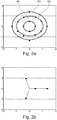
- However, in case of a 16-Quadrature Amplitude Modulation (16-QAM) format represented in
fig.2a , the application of a fourth power to the constellation symbols leads to the resulting signal offig.2b wherein non-real and non-positive symbols remain (dotted arrows). The non-real and non-positive symbols correspond to the middle ring symbols of the 16-QAM constellation infig.2a . - One solution to overcome this problem is to apply a radius directed algorithm wherein some of the received symbols (the symbols from the middle ring, which after the 4th power computation are not real and positive) are not taken into account in the carrier frequency estimation. However, such solution requires a long averaging process, as it rejects roughly 50% of the signals, which is not suitable for high speed optical interfaces and is not optimal as a part of the data is not used in the carrier frequency estimation.
- It is therefore a goal of the present invention to provide a solution enabling carrier frequency estimation in high speed optical networks using constellation shaping.
- Thus, the invention refers to a method for estimating a carrier frequency offset at the reception of an optical signal modulated in amplitude and phase, the signal comprising a series of modulation symbols, the method comprising the following steps:
- computing a Mth power of the modulation symbols of the signal wherein the number M is predetermined according to the modulation format in order to remove the modulation effects on the carrier signal, the computation leading to the establishment of Mth power resulting states,
- for the different Mth power resulting states, applying a predetermined correction factor depending on the phase and/or the amplitude of the given Mth power resulting state to provide corrected states,
- calculating a predetermined estimator of the carrier frequency offset based on the corrected states.
- According to an aspect of the present invention, the modulation format corresponds to a modulation format based on constellation shaping.
- According to an aspect of the present invention, the predetermined estimator is the frequency f that maximizes the expression

- According to another aspect of the present invention, the function f is computed for N equally spaced frequencies by a fast fourier transform "FFT" of the corrected states.
- According to an aspect of the present invention, the predetermined correction factor is a sign correction factor for the Mth power resulting states located in the left hemisphere of the complex plane in the absence of phase and frequency shift.
- According to an aspect of the present invention, the sign correction factor depends on the amplitude of the modulation symbols.
- According to an aspect of the present invention, the predetermined correction factor is a weighted factor based on a calculated variance of an estimated phase of the different Mth power resulting states.
- According to an aspect of the present invention, the variance of the estimated phase of the different Mth power resulting states depends on their amplitude.
- According to an aspect of the present invention, the modulation format corresponds to a square quadrature amplitude modulation "QAM" format and wherein the number M of the power is equal to four.
- According to an aspect of the present invention, the method comprises the following preliminary steps:
- filtering the incoming symbols by amplitude,
- assigning each amplitude level a phase estimator variance,
- assigning each amplitude level a phase estimator sign,
- determining the correction factor based on the assigned phase estimator variance and phase estimator sign.
- The present invention also refers to a method for detecting a received optical signal modulated in amplitude and phase wherein the method comprises the following steps:
- a coherent mixing step wherein the received optical signal is mixed with the signal of a local oscillator to produce a mixed signal,
- a conversion step wherein the in-phase and quadrature parts of the different polarizations of the mixed signal are converted to digital signals,
- a deskew and resampling step,
- a chromatic dispersion step,
- a timing recovery step for recovering the frequency of the modulated signal,
- a polarization demultiplexing step,
- a carrier frequency estimation step as described previously,
- a carrier phase estimation step,
- a demapping step.
- The present invention also refers to a processing unit configured for estimating a carrier frequency of a received optical signal modulated in amplitude and phase, the signal comprising a series of modulation symbols and the processing unit being configured for:
- computing a Mth power of the modulation symbols of the signal wherein the number M is predetermined according to the modulation format in order to remove the modulation effects on the carrier signal, the computation leading to the establishment of Mth power resulting states;
- for the resulting states, applying a predetermined correction factor depending on the phase and/or the amplitude of the given Mth power resulting states state to provide corrected states,
- calculating a predetermined estimator of the carrier frequency offset based on the corrected states.
- The present invention also refers to an optical receiver comprising:
- a coherent mixer linked to a local oscillator and configured for mixing a received signal with the signal of the local oscillator to produce a mixed signal,
- a plurality of photo-diodes for detecting the in-phase and the quadrature parts of the different polarization,
- a plurality of analog-to-digital conversion units associated to the respective plurality of photo-diodes,
- a processing unit as described previously and configured for:
- applying a deskew and resampling,
- applying chromatic dispersion compensation,
- estimating the modulation frequency,
- applying a constant modulus algorithm for polarization demultiplexing,
- estimating a carrier phase,
- applying a demapping.
-
-
FIG.1a is a constellation diagram corresponding to a QPSK (or 4-QAM) modulation format, -
FIG.1b is the constellation diagram offig.1a after application of a 4th power operation, -
FIG.2a is a constellation diagram corresponding to a 16-QAM modulation format, -
FIG.2b is the constellation diagram offig.2a after application of a 4th power operation, -
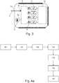
FIG.3 is a diagram of a receiver, -
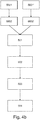
FIG.4a is a flowchart of the steps of the digital signal processing at the receiver, -
FIG.4b is a flowchart of the sub-steps of a frequency offset recovery step, -
FIG.5a represents a graph of the number of transmitted symbols as a function of their amplitude in the case of a 16-QAM modulation, -
FIG.5b represents a graph of the estimated phase of transmitted symbols as a function of their amplitude in the case of a 16-QAM modulation, -
FIG.5c represents a graph of the estimated sign of transmitted symbols as a function of their amplitude in the case of a 16-QAM modulation, -
FIG.6a represents a graph of the number of transmitted symbols as a function of their amplitude in the case of a 64-QAM modulation, -
FIG.6b represents a graph of the estimated phase of transmitted symbols as a function of their amplitude in the case of a 64-QAM modulation, -
FIG.6c represents a graph of the estimated sign of transmitted symbols as a function of their amplitude in the case of a 64-QAM modulation. - The following achievements are examples. Although, the specification refers to one or several embodiments, it does not imply that each reference refers to the same embodiment or that the features apply only to a single embodiment. Simple features of different embodiments can also be combined to provide other embodiments.
-
Fig.3 discloses the structure of anoptical receiver 1 based on a coherent detection. Theoptical receiver 1 comprises alocal oscillator 3, generally a tunable laser source and acoherent mixer 5. Thecoherent mixer 5 comprises afirst input 5a linked to theinput 1a of theoptical receiver 1 which is generally connected to an optical transmission mean such as an optical fiber 7 and asecond input 5b linked to thelocal oscillator 3. Thelocal oscillator 3 is set at the same frequency as the signal received on theinput 1a in order to enable the detection of the said received signal. Thecoherent mixer 5 is configured for mixing the incoming signal received from the optical fiber 7 and the signal produced by thelocal oscillator 3. Theoptical receiver 1 also comprises a plurality (four in the present case) ofoptical detectors 9 such as photo-diodes configured for detecting the different parts (in-phase and quadrature parts of the different polarizations) of the mixed signal. Theoptical receiver 1 also comprises a plurality of analog to digital conversion units 11 configured to convert the signals detected by theoptical detectors 9 into digital signals in order to apply digital signal processing on these signals. Theoptical receiver 1 also comprises a digital processing unit 13. The digital processing unit 13 refers for example to a processor. -
Fig.4a represents the different steps of the digital signal processing. - The
first step 101 refers to a deskew and resampling step. - The
second step 102 refers to a chromatic dispersion step. - The
third step 103 refers to a timing recovery step wherein the modulation frequency is recovered. - The
fourth step 104 refers to a polarization demultipexing step. Such polarization demultiplexing is for example achieved by a constant modulus algorithm. - The
fifth step 105 refers to a frequency offset recovery configured for estimating the data signal frequency of the transmitted signal and for compensating the frequency detuning between the incoming signal frequency and the local oscillator frequency. - The
sixth step 106 refers to a carrier phase recovery wherein the phase noise is filtered in order to retrieve the carrier phase. - The
seventh step 107 refers to a demapping step wherein the constellation symbols are converted into data bits. - The present invention deals more specifically with the
fifth step 105 and the frequency offset recovery when the incoming signal is modulated in amplitude and phase, for example when quadrature phase shift keying (QPSK) or quadrature amplitude modulation (QAM) format are used for the transmission of the optical signals. The present invention is particularly interesting when constellation shaping is used. The present invention refers to the application of a predetermined correction factor on the constellation symbols corresponding to the Mth power of the received modulation symbols, the predetermined correction factor being dependent of the amplitude and/or of the phase of the transmitted modulation symbols. - The different sub-steps of the frequency offset
recovery step 105 will now be described based onfig.4b . - The
first sub-step 501 corresponds to the filtering of the modulation symbols of the incoming signals by amplitude. The amplitude corresponds to the distance of a symbol from the origin in the constellation diagram. - The
second sub-step 502 refers to the computation of a Mth power of the signal leading to Mth power resulting states. The number M is predetermined according to the modulation format in order to remove the modulation effects on the carrier signal. For example, in the case of a square-QAM modulation, such as a 16-QAM modulation, a fourth power can be used. Thus, the periodogram represents the Mth power of each of the transmitted symbols. - The third sub-step 503 corresponds to the application of a predetermined correction factor for the different Mth power resulting states. The correction factor depends for example on the phase or on the amplitude or both the phase and the amplitude of the given Mth power resulting state. The application of the correction factor provides a corrected state.
- The
fourth sub-step 504 refers to the calculation of a predetermined estimator of the carrier frequency offset based on the corrected states. The predetermined estimator corresponds to the frequency f that maximize the expression defined by: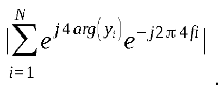
This sum can be implemented in an efficient manner for a set of N equally-spaced frequencies with the use of the Fast Fourier Transform (FFT) of N points. - According to a first embodiment, the predetermined correction factor in the third sub-step 503 corresponds to a sign correction factor wherein a negative sign is applied to the incoming modulation symbols having a predetermined amplitude. Indeed, the modulation symbols leading to a negative sign are the modulation symbols of the middle ring in the 16-QAM constellation represented in
fig.2a . Indeed, with the 16-QAM constellation offig.2a , the different symbols can be gathered in three rings, an inner ring noted R1, a middle ring noted R2 and an outer ring noted R3, each ring corresponding to a common amplitude of the symbols corresponding to the distance between the symbols of a ring and the origin of the graph. As a consequence, for the received modulation symbols having an amplitude corresponding to the middle ring R2, a negative sign is applied as correction factor. Indeed, these symbols correspond to the 4th power resulting states (after application of a 4th power operation) that are located in the left hemisphere of the complex plane (states associated with the dotted arrows infig.2b ) so that a sign correction is required to switch them in the right hemisphere of the complex plane. In order to determine the range of amplitude for which a negative sign is applied, many noisy symbols, 16-QAM symbols in the present case, can be studied and classified according to their amplitude. - Furthermore, concerning the fact that the middle ring R2 constellation symbols lead to imaginary symbols when the fourth power is applied as represented by the dotted arrows in
fig.2b , it has to be observed that the vectorial sum of these arrows lead to a real value. As a consequence, by applying a negative sign and by summing the contribution of the constellation symbols of the middle ring, it is possible to use their contribution to estimate the frequency offset. In such case, the frequency estimator is given by the frequency f that maximizes the following expression:
- Thus, with such embodiment, a
preliminary step 5001 of assigning a sign correction factor to each amplitude level is achieved. Such preliminary step is for example based on statistics made on a high number of transmitted symbols. - The correction factor is then determined based on the assigned sign estimator in an another
preliminary step 5002. - According to a second embodiment, the predetermined correction factor corresponds to a sign and variance correction factor. As disclosed previously, the variance function can be determined based on statistics made on many noisy symbols wherein the phase of the noisy symbols after application of a 4th power operation is determined and wherein an estimator corresponding to the variance of the obtained phases according to the amplitude of the symbols can then be determined and used as a phase variance estimator which can be used for the transmitted symbols processing.
- For example, in the case of the 16-QAM modulation, many 16-QAM noisy symbols are considered to produce an amplitude histogram showing the distribution of the different symbols according to their amplitude.
Fig.5a represents such histogram. The vertical lines at amplitudes 0.45, 1 and 1.35 represent the theoretical amplitudes of the respectively inner ring R1, middle ring R2 and outer ring R3 of the constellation diagram offig.2a . The middle ring R2 comprises 8 different symbols whereas the inner R1 and outer R3 rings comprise 4 different symbols which explains a higher peak associated to the amplitude of 1. -
Fig.5b represents the variance in the phase estimator as a function of the amplitude, the horizontal line represents the variance in the case of a random phase. The variance appears to be a weighting factor so that the lower the variance, the higher the confidence to the associated symbols. -
Fig.5c represents the sign correction factor as a function of the amplitude. The sign factor is either equals to 1 or to -1. Thus, in order to obtain the best estimation for the frequency is to use an estimator combining the variance obtained infig.5b and the sign obtained infig.5c . In such case, the estimators are given by the following expressions: and
- Thus, with such embodiment, a preliminary step 5001' of assigning a sign correction factor and a variance correction factor to each amplitude level is achieved. Such preliminary step is for example based on statistics made on a high number of transmitted symbols. The correction factor is then determined based on the assigned phase correction factor and sign correction factor in an another preliminary step 5002'.
- Such estimators enable estimating the frequency offset taking into account the contribution of all the symbols. Furthermore, it can be seen that the higher the amplitude of the symbols, the lower the variance. Indeed, for a given gap between the real position of a symbol and its theoretical position in the periodogram, noise corruption over a symbol having a higher amplitude would lead to a smaller shift of the phase of the symbols and therefore to a better accuracy of the estimated frequency. A higher confidence is therefore given to the symbols of higher amplitude. The variance is also higher in the region where the sign estimator is switched from -1 to 1 (or from 1 to -1), where there is too much uncertainty of which ring the received signal belong.
- The above disclosed method is not limited to 16-QAM modulation symbols but may be applied to any modulation format comprising a phase and amplitude modulation.
Fig.6a, 6b and 6c represent respectively the graphs of the number of symbols, the variance in the phase estimator and the sign estimator (corresponding to the graphs described inFIG. 5 a to 5c) in the case of a transmission based on a 64-QAM modulation format. The 64-QAM modulation format constellation comprises a higher number of rings (seven rings) but the same method can be applied to recover the frequency offset. - The application of a correction factor taking into account the sign and/or the variance enables therefore providing a better estimation of the carrier frequency offset and consequently fewer samples are required to achieve the same estimation performance. The overall quality of the transmission is therefore enhanced.
- The functions of the various elements shown in the FIGs., including any functional blocks labeled as "processors" or "processing units", may be provided through the use of dedicated hardware as well as hardware capable of executing software in association with appropriate software. When provided by a processor, the functions may be provided by a single dedicated processor, by a single shared processor, or by a plurality of individual processors, some of which may be shared. Moreover, explicit use of the term "processor" or "controller" should not be construed to refer exclusively to hardware capable of executing software, and may implicitly include, without limitation, digital signal processor (DSP) hardware, network processor, application specific integrated circuit (ASIC), field programmable gate array (FPGA), read only memory (ROM) for storing software, random access memory (RAM), and non volatile storage. Other hardware, conventional and/or custom, may also be included. Similarly, any switches shown in the FIGS. are conceptual only. Their function may be carried out through the operation of program logic, through dedicated logic, through the interaction of program control and dedicated logic, or even manually, the particular technique being selectable by the implementer as more specifically understood from the context.
Claims (12)
- Method for estimating a carrier frequency offset (105) at the reception of an optical signal modulated in amplitude and phase, the signal comprising a series of modulation symbols and the method comprising:- computing a Mth power of the modulation symbols of the signal (502) wherein the number M is predetermined according to the modulation format in order to remove the modulation effects on the carrier signal, the computation leading to the establishment of Mth power resulting states,- for the different Mth power resulting states, applying a predetermined correction factor depending on the phase and/or the amplitude of the given Mth power resulting state to provide corrected states (503),- calculating a predetermined estimator of the carrier frequency offset based on the corrected states (504).
- Method in accordance with claim 1 wherein the modulation format corresponds to a modulation format based on constellation shaping.
- Method in accordance with claim 1 or 2 wherein the predetermined estimator is the frequency f that maximizes the expression

- Method in accordance with claim 3 wherein the function f is computed for N equally spaced frequencies by a fast fourier transform "FFT" of the corrected states.
- Method in accordance with one of the previous claims wherein the predetermined correction factor is a sign correction factor for the Mth power resulting states located in the left hemisphere of the complex plane.
- Method in accordance with one of the previous claims wherein the predetermined correction factor is a weighted factor based on a calculated variance of an estimated phase of the different Mth power resulting states.
- Method in accordance with claim 6 wherein the variance of the estimated phase of the different Mth power resulting states depends on their amplitude.
- Method in accordance with one of the previous claims wherein the modulation format corresponds to a square quadrature amplitude modulation "QAM" format and wherein the number M of the power is equal to four.
- Method in accordance with one of the previous claims wherein it comprises the following preliminary steps:- filtering the incoming symbols by amplitude (501),- assigning each amplitude level a phase estimator variance (5001'),- assigning each amplitude level a phase estimator sign (5001'), [same thing for the sign?]- determining the correction factor based on the assigned phase estimator variance and phase estimator sign (5002').
- Method for detecting a received optical signal modulated in amplitude and phase wherein the method comprises the following steps:- a coherent mixing step wherein the received optical signal is mixed with the signal of a local oscillator (3) to produce a mixed signal,- a conversion step wherein the in-phase and quadrature parts of the different polarizations of the mixed signal are converted to digital signals,- a deskew and resampling step (101),- a chromatic dispersion step (102),- a timing recovery step for recovering the frequency of the modulated signal (103),- a polarization demultiplexing step (104),- a carrier frequency estimation step (105) in accordance with one of the previous claims,- a carrier phase estimation step (106),- a demapping step (107).
- Processing unit (13) configured for estimating a carrier frequency offset of a received optical signal modulated in amplitude and phase, the signal comprising a series of modulation symbols and the processing unit (13) being configured for:- computing a Mth power of the modulation symbols of the signal wherein the number M is predetermined according to the modulation format in order to remove the modulation effects on the carrier signal (502), the computation leading to the establishment of Mth power resulting states,- for the different Mth power resulting states, applying a predetermined correction factor depending on the phase and/or the amplitude of the given Mth power resulting state to provide corrected states (503),- calculating a predetermined estimator of the carrier frequency offset based on the corrected states (504).
- Optical receiver (1) comprising:- a coherent mixer (5) linked to a local oscillator (3) and configured for mixing a received signal with the signal of the local oscillator (3) to produce a mixed signal,- a plurality of photo-diodes (9) for detecting the in-phase and the quadrature parts of the different polarization,- a plurality of analog-to-digital conversion units (11) associated to the respective plurality of photo-diodes (9),- a processing unit (13) in accordance with claim 10 also configured for:- applying a deskew and resampling (101),- applying chromatic dispersion compensation (102),- estimating the modulation frequency (103),- applying a constant modulus algorithm for polarization demultiplexing (104),- estimating a carrier phase (106),- applying a demapping (107).
Priority Applications (1)
| Application Number | Priority Date | Filing Date | Title |
|---|---|---|---|
| EP17306092.2A EP3447939A1 (en) | 2017-08-24 | 2017-08-24 | Carrier frequency estimation method and associated processing unit, detection method and associated receiver |
Applications Claiming Priority (1)
| Application Number | Priority Date | Filing Date | Title |
|---|---|---|---|
| EP17306092.2A EP3447939A1 (en) | 2017-08-24 | 2017-08-24 | Carrier frequency estimation method and associated processing unit, detection method and associated receiver |
Publications (1)
| Publication Number | Publication Date |
|---|---|
| EP3447939A1 true EP3447939A1 (en) | 2019-02-27 |
Family
ID=59772564
Family Applications (1)
| Application Number | Title | Priority Date | Filing Date |
|---|---|---|---|
| EP17306092.2A Withdrawn EP3447939A1 (en) | 2017-08-24 | 2017-08-24 | Carrier frequency estimation method and associated processing unit, detection method and associated receiver |
Country Status (1)
| Country | Link |
|---|---|
| EP (1) | EP3447939A1 (en) |
Citations (1)
| Publication number | Priority date | Publication date | Assignee | Title |
|---|---|---|---|---|
| US20150200731A1 (en) * | 2014-01-14 | 2015-07-16 | Cisco Technology, Inc. | Sub-Sampled Carrier Phase Recovery |
-
2017
- 2017-08-24 EP EP17306092.2A patent/EP3447939A1/en not_active Withdrawn
Patent Citations (1)
| Publication number | Priority date | Publication date | Assignee | Title |
|---|---|---|---|---|
| US20150200731A1 (en) * | 2014-01-14 | 2015-07-16 | Cisco Technology, Inc. | Sub-Sampled Carrier Phase Recovery |
Non-Patent Citations (3)
| Title |
|---|
| BILAL SYED MUHAMMAD ET AL: "Carrier Phase Estimation Through the Rotation Algorithm for 64-QAM Optical Systems", JOURNAL OF LIGHTWAVE TECHNOLOGY, IEEE SERVICE CENTER, NEW YORK, NY, US, vol. 33, no. 9, 1 May 2015 (2015-05-01), pages 1766 - 1773, XP011576045, ISSN: 0733-8724, [retrieved on 20150317], DOI: 10.1109/JLT.2015.2402441 * |
| TADAO NAKAGAWA ET AL: "Non-data-aided wide-range frequency offset estimator for QAM optical coherent receivers", 2011 OPTICAL FIBER COMMUNICATION CONFERENCE AND EXPOSITION AND THE NATIONAL FIBER OPTIC ENGINEERS CONFERENCE (OFC/NFOEC 2011) : LOS ANGELES, CALIFORNIA, USA, 6 - 10 MARCH 2011, IEEE, PISCATAWAY, NJ, USA, 6 March 2011 (2011-03-06), pages 1 - 3, XP031946233, ISBN: 978-1-4577-0213-6 * |
| YULIANG GAO ET AL: "Low-complexity two-stage carrier phase estimation for 16-QAM systems using QPSK partitioning and maximum likelihood detection", 2011 OPTICAL FIBER COMMUNICATION CONFERENCE AND EXPOSITION AND THE NATIONAL FIBER OPTIC ENGINEERS CONFERENCE (OFC/NFOEC 2011) : LOS ANGELES, CALIFORNIA, USA, 6 - 10 MARCH 2011, IEEE, PISCATAWAY, NJ, USA, 6 March 2011 (2011-03-06), pages 1 - 3, XP031946238, ISBN: 978-1-4577-0213-6 * |
Similar Documents
| Publication | Publication Date | Title |
|---|---|---|
| CN108512802B (en) | Circuit, method and receiving device for in-phase and quadrature phase mismatch compensation | |
| RU2511719C2 (en) | Carrier recovery circuit and demodulation circuit based on quasi-coherent detection method | |
| US8781029B2 (en) | Frequency offset estimation apparatus, reception apparatus, frequency offset estimation method, and reception method | |
| EP3432488B1 (en) | Transmission characteristic compensation device, transmission characteristic compensation method, and communication device | |
| US8660438B2 (en) | Digital coherent receiver and receiving method | |
| US20120155890A1 (en) | Complexity reduced feed forward carrier recovery methods for m-qam modulation formats | |
| EP1777906A1 (en) | Amplitude error compensating apparatus and orthogonality error compensating apparatus | |
| GB2313270A (en) | Digital Broadcasting Receiver | |
| EP2583424B1 (en) | Method for phase and oscillator frequency estimation | |
| JP2018042219A (en) | Receiver and phase error compensation method | |
| JPH09219693A (en) | Digital broadcast receiver | |
| CN102027696A (en) | Filter coefficient control device and method | |
| CN103430003A (en) | Method for estimating a chromatic dispersion of a received optical signal | |
| CA3012977C (en) | Phase compensation device, phase compensation method and communication apparatus | |
| CN104486272A (en) | Feedback signal correcting method and device | |
| JP6024531B2 (en) | Frequency error estimating apparatus and method, frequency error compensating apparatus, and optical receiver | |
| CN102647381A (en) | Method and device for elevating frequency deviation in MPSK (Mary Phase Shift Keying) coherent light communication system | |
| US20190123832A1 (en) | Phase recovery for signals with quadrature amplitude modulation | |
| US8155244B2 (en) | Demodulation using blind constellation identification for communication signals | |
| CN109246044B (en) | Frequency offset estimation method and system for 32-ary quadrature amplitude modulated signal | |
| EP2337294B1 (en) | IQ-imbalance estimation for non-symmetrical pilot symbols | |
| JP3851143B2 (en) | MODULATION SYSTEM IDENTIFICATION CIRCUIT, RECEPTION DEVICE EQUIPPED WITH SAME, WIRELESS STATION, AND MODULATION SYSTEM IDENTIFICATION METHOD | |
| JP3983688B2 (en) | Modulation type identification circuit and demodulator | |
| WO2020174656A1 (en) | Reception signal processing device, reception signal processing method, and optical receiver | |
| EP2624514B1 (en) | Removal of a band-limited distributed pilot from an ofdm signal |
Legal Events
| Date | Code | Title | Description |
|---|---|---|---|
| PUAI | Public reference made under article 153(3) epc to a published international application that has entered the european phase |
Free format text: ORIGINAL CODE: 0009012 |
|
| AK | Designated contracting states |
Kind code of ref document: A1 Designated state(s): AL AT BE BG CH CY CZ DE DK EE ES FI FR GB GR HR HU IE IS IT LI LT LU LV MC MK MT NL NO PL PT RO RS SE SI SK SM TR |
|
| AX | Request for extension of the european patent |
Extension state: BA ME |
|
| RAP1 | Party data changed (applicant data changed or rights of an application transferred) |
Owner name: NOKIA SOLUTIONS AND NETWORKS OY |
|
| 17P | Request for examination filed |
Effective date: 20190827 |
|
| RBV | Designated contracting states (corrected) |
Designated state(s): AL AT BE BG CH CY CZ DE DK EE ES FI FR GB GR HR HU IE IS IT LI LT LU LV MC MK MT NL NO PL PT RO RS SE SI SK SM TR |
|
| GRAP | Despatch of communication of intention to grant a patent |
Free format text: ORIGINAL CODE: EPIDOSNIGR1 |
|
| INTG | Intention to grant announced |
Effective date: 20200128 |
|
| RIN1 | Information on inventor provided before grant (corrected) |
Inventor name: RIOS MULLER, RAFAEL Inventor name: RENAUDIER, JEREMIE |
|
| STAA | Information on the status of an ep patent application or granted ep patent |
Free format text: STATUS: THE APPLICATION IS DEEMED TO BE WITHDRAWN |
|
| 18D | Application deemed to be withdrawn |
Effective date: 20200609 |