EP3447917A1 - Bidirectional switch with passive electrical network for substrate potential stabilization - Google Patents
Bidirectional switch with passive electrical network for substrate potential stabilization Download PDFInfo
- Publication number
- EP3447917A1 EP3447917A1 EP18188581.5A EP18188581A EP3447917A1 EP 3447917 A1 EP3447917 A1 EP 3447917A1 EP 18188581 A EP18188581 A EP 18188581A EP 3447917 A1 EP3447917 A1 EP 3447917A1
- Authority
- EP
- European Patent Office
- Prior art keywords
- input
- switching device
- bidirectional switch
- output terminal
- capacitance
- Prior art date
- Legal status (The legal status is an assumption and is not a legal conclusion. Google has not performed a legal analysis and makes no representation as to the accuracy of the status listed.)
- Granted
Links
Images




Classifications
-
- H—ELECTRICITY
- H03—ELECTRONIC CIRCUITRY
- H03K—PULSE TECHNIQUE
- H03K17/00—Electronic switching or gating, i.e. not by contact-making and –breaking
- H03K17/16—Modifications for eliminating interference voltages or currents
- H03K17/161—Modifications for eliminating interference voltages or currents in field-effect transistor switches
-
- H—ELECTRICITY
- H03—ELECTRONIC CIRCUITRY
- H03K—PULSE TECHNIQUE
- H03K17/00—Electronic switching or gating, i.e. not by contact-making and –breaking
- H03K17/06—Modifications for ensuring a fully conducting state
- H03K17/063—Modifications for ensuring a fully conducting state in field-effect transistor switches
-
- H—ELECTRICITY
- H10—SEMICONDUCTOR DEVICES; ELECTRIC SOLID-STATE DEVICES NOT OTHERWISE PROVIDED FOR
- H10D—INORGANIC ELECTRIC SEMICONDUCTOR DEVICES
- H10D30/00—Field-effect transistors [FET]
- H10D30/40—FETs having zero-dimensional [0D], one-dimensional [1D] or two-dimensional [2D] charge carrier gas channels
- H10D30/47—FETs having zero-dimensional [0D], one-dimensional [1D] or two-dimensional [2D] charge carrier gas channels having two-dimensional [2D] charge carrier gas channels, e.g. nanoribbon FETs or high electron mobility transistors [HEMT]
- H10D30/471—High electron mobility transistors [HEMT] or high hole mobility transistors [HHMT]
- H10D30/475—High electron mobility transistors [HEMT] or high hole mobility transistors [HHMT] having wider bandgap layer formed on top of lower bandgap active layer, e.g. undoped barrier HEMTs such as i-AlGaN/GaN HEMTs
- H10D30/4755—High electron mobility transistors [HEMT] or high hole mobility transistors [HHMT] having wider bandgap layer formed on top of lower bandgap active layer, e.g. undoped barrier HEMTs such as i-AlGaN/GaN HEMTs having wide bandgap charge-carrier supplying layers, e.g. modulation doped HEMTs such as n-AlGaAs/GaAs HEMTs
-
- H—ELECTRICITY
- H10—SEMICONDUCTOR DEVICES; ELECTRIC SOLID-STATE DEVICES NOT OTHERWISE PROVIDED FOR
- H10D—INORGANIC ELECTRIC SEMICONDUCTOR DEVICES
- H10D84/00—Integrated devices formed in or on semiconductor substrates that comprise only semiconducting layers, e.g. on Si wafers or on GaAs-on-Si wafers
- H10D84/01—Manufacture or treatment
-
- H—ELECTRICITY
- H10—SEMICONDUCTOR DEVICES; ELECTRIC SOLID-STATE DEVICES NOT OTHERWISE PROVIDED FOR
- H10D—INORGANIC ELECTRIC SEMICONDUCTOR DEVICES
- H10D84/00—Integrated devices formed in or on semiconductor substrates that comprise only semiconducting layers, e.g. on Si wafers or on GaAs-on-Si wafers
- H10D84/80—Integrated devices formed in or on semiconductor substrates that comprise only semiconducting layers, e.g. on Si wafers or on GaAs-on-Si wafers characterised by the integration of at least one component covered by groups H10D12/00 or H10D30/00, e.g. integration of IGFETs
- H10D84/811—Combinations of field-effect devices and one or more diodes, capacitors or resistors
-
- H—ELECTRICITY
- H03—ELECTRONIC CIRCUITRY
- H03K—PULSE TECHNIQUE
- H03K2217/00—Indexing scheme related to electronic switching or gating, i.e. not by contact-making or -breaking covered by H03K17/00
- H03K2217/0009—AC switches, i.e. delivering AC power to a load
-
- H—ELECTRICITY
- H03—ELECTRONIC CIRCUITRY
- H03K—PULSE TECHNIQUE
- H03K2217/00—Indexing scheme related to electronic switching or gating, i.e. not by contact-making or -breaking covered by H03K17/00
- H03K2217/0018—Special modifications or use of the back gate voltage of a FET
-
- H—ELECTRICITY
- H03—ELECTRONIC CIRCUITRY
- H03K—PULSE TECHNIQUE
- H03K2217/00—Indexing scheme related to electronic switching or gating, i.e. not by contact-making or -breaking covered by H03K17/00
- H03K2217/0036—Means reducing energy consumption
-
- H—ELECTRICITY
- H03—ELECTRONIC CIRCUITRY
- H03K—PULSE TECHNIQUE
- H03K2217/00—Indexing scheme related to electronic switching or gating, i.e. not by contact-making or -breaking covered by H03K17/00
- H03K2217/0054—Gating switches, e.g. pass gates
-
- H—ELECTRICITY
- H10—SEMICONDUCTOR DEVICES; ELECTRIC SOLID-STATE DEVICES NOT OTHERWISE PROVIDED FOR
- H10D—INORGANIC ELECTRIC SEMICONDUCTOR DEVICES
- H10D30/00—Field-effect transistors [FET]
- H10D30/60—Insulated-gate field-effect transistors [IGFET]
- H10D30/611—Insulated-gate field-effect transistors [IGFET] having multiple independently-addressable gate electrodes influencing the same channel
-
- H—ELECTRICITY
- H10—SEMICONDUCTOR DEVICES; ELECTRIC SOLID-STATE DEVICES NOT OTHERWISE PROVIDED FOR
- H10D—INORGANIC ELECTRIC SEMICONDUCTOR DEVICES
- H10D62/00—Semiconductor bodies, or regions thereof, of devices having potential barriers
- H10D62/80—Semiconductor bodies, or regions thereof, of devices having potential barriers characterised by the materials
- H10D62/82—Heterojunctions
- H10D62/824—Heterojunctions comprising only Group III-V materials heterojunctions, e.g. GaN/AlGaN heterojunctions
Definitions
- the instant application generally relates to semiconductor devices, and more particularly relates to bidirectional high electron mobility transistors.
- MOSFET Metal Insulator Semiconductor Field Effect Transistor
- HEMT high-electron-mobility Field Effect Transistor
- HFET heterostructure FET
- MODFET modulation-doped FET
- HEMTs are viewed as an attractive candidate for power transistor applications, i.e., applications in which switching of substantially large voltages and/or currents is required.
- HEMTs offer high conduction and low resistive losses in comparison to conventional silicon based devices.
- HEMTs are commonly formed from III-V semiconductor materials, such as GaN, GaAs, InGaN, AlGaN, etc.
- a two-dimensional electron gas (2DEG) arises at the interface between the AlGaN barrier layer and the GaN buffer layer.
- the 2DEG forms the channel of the device instead of a doped region, which forms the channel in a conventional MOSFET device.
- Similar principles may be utilized to select buffer and barrier layers that form a two-dimensional hole gas (2DHG) as the channel of the device.
- a 2DEG or a 2DHG is generally referred to as a two-dimensional carrier gas.
- the heterojunction configuration leads to a self-conducting, i.e., normally-on, transistor.
- Normally-off structures are also possible. In these cases, measures must be taken to prevent the channel region of an HEMT from being in a conductive state in the absence of a positive gate voltage.
- a bidirectional switch is a device that is capable of switching voltages of positive or negative polarity. That is, a bidirectional switch is configured to control current flow in both directions.
- a dual gate type III-V semiconductor bidirectional switch can be realized by providing two HEMT gate structures in series between two electrically conductive terminals that are in contact with the two-dimensional carrier gas. The two HEMTs can share the same drift region (the resistive voltage sustaining part) of the device which means the on-state resistance can be approximately half of a conventional back to back device.
- bidirectional switches relates to capacitive coupling between the channel of the device and the underlying semiconductor substrate.
- the underlying semiconductor substrate is typically tied to the reference potential terminal (e.g., the source terminal) of the device by substrate contacts.
- the reference potential terminal e.g., the source terminal
- the same benefit cannot be obtained using a simple electrical contact in the case of a bidirectional switch because there is not a single terminal that is maintained at a reference potential in all states of operations; the voltage polarity across the device changes.
- Known solutions to this problem suffer from various drawbacks.
- the semiconductor device includes a semiconductor body having an active region and a substrate region that is disposed beneath the active region.
- a bidirectional switch is formed in the semiconductor body and is configured to block voltage across two polarities.
- the bidirectional switch includes first and second gate structures that are each configured to control a conductive state of an electrically conductive channel that is disposed in the upper active region, and first and second input-output terminals that are each in ohmic contact with the electrically conductive channel.
- a first switching device is configured to electrically connect the substrate region to the first input-output terminal.
- a second switching device is configured to electrically connect the substrate region to the second input- output terminal.
- a passive electrical network includes a first capacitance and a second capacitance.
- the first capacitance is connected between a control terminal of the second switching device and the first input-output terminal.
- the second capacitance is connected between a control terminal of the first switching device and the second input-output terminal.
- the passive electrical network is configured to temporarily electrically connect the substrate region to the second input-output terminal by turning the second switching device on when the second input-output terminal is at a higher potential than the first input-output terminal.
- the passive electrical network is configured to temporarily electrically connect the substrate region to the first input-output terminal by turning the first switching device on when the first input-output terminal is at a higher potential than the second input-output terminal.
- the first and second switching devices are current controlled switches, wherein the first capacitance is configured to supply a temporary current to the control terminal of the second switching device during a transition of the bidirectional switch from a blocking state to a conducting state at a first voltage polarity of the bidirectional switch, and wherein the second capacitance is configured to supply a temporary current to the control terminal of the first switching device during a transition of the bidirectional switch from a blocking state to a conducting state at a second voltage polarity of the bidirectional switch, the second voltage polarity being opposite from the first voltage polarity.
- the semiconductor body comprises a type III semiconductor nitride, wherein the bidirectional switch is a high electron mobility transistor, and wherein the electrically conductive channel is a two-dimensional charge carrier gas.
- the first and second switching devices are high-electron-mobility transistors that are integrally formed in the semiconductor body.
- the first capacitance is exclusively connected between the control terminal of the second switching device and the first input-output terminal, and wherein the second capacitance is exclusively connected between the control terminal of the first switching device and the second input-output terminal.
- the passive electrical network further comprises a first voltage limiting element connected between the substrate region and an input of the first switching device, a second voltage limiting element connected between the substrate region and an input of the first switching device, wherein the first voltage limiting element is configured to limit a voltage applied to the control terminal of the first switching device to below a maximum rated input voltage of the first switching device, and wherein the second voltage limiting element is configured to limit a voltage applied to the control terminal of the second switching device to below a maximum rated input voltage of the second switching device.
- the first and second switching devices are integrated within the semiconductor body.
- the passive electrical network is integrated within the semiconductor body and is exclusively connected to the first and second input-output terminals, the first and second switching devices and the substrate region.
- the semiconductor device includes a semiconductor body having an active region and a substrate region that is disposed beneath the active region.
- a bidirectional switch is formed in the semiconductor body and is configured to block voltage across two polarities.
- the bidirectional switch includes first and second gate structures that are each configured to control a conductive state of an electrically conductive channel that is disposed in the upper active region, and first and second input-output terminals that are each in ohmic contact with the electrically conductive channel.
- a first switching device is configured to electrically connect the substrate region to the first input-output terminal when turned on.
- a second switching device is configured to electrically connect the substrate region to the second input-output terminal when turned on.
- a passive electrical network is configured to generate a first substrate reference signal that turns the second switching device on during a first transitional state of the bidirectional switch and to generate a second substrate reference signal that turns the first switching device on during a second transitional state of the bidirectional switch.
- the first transitional state is a state when the second input-output terminal is at a higher potential than the first input-output terminal and the bidirectional switch is turned on
- the second transitional state is a state when the first input-output terminal is at a higher potential than the second input-output terminal and the bidirectional switch is turned on.
- the self-biasing passive electrical network comprises a first capacitance and a second capacitance, the first capacitance being connected between a control terminal of the second switching device and the first input-output terminal, the second capacitance being connected between a control terminal of the first switching device and the second input-output terminal, wherein the first capacitance is configured to provide the first substrate reference signal during the first transitional state, and wherein the second capacitance is configured to provide the second substrate reference signal during the second transitional state.
- the first and second switching devices are current controlled switches, wherein the self-biasing passive electrical network is configured to generate the first substrate reference signal by providing a temporary current pulse at the control terminal of the second switching device from a redistribution of charges occurring during the first transitional state, and wherein the self-biasing passive electrical network is configured to generate the second substrate reference signal by providing a temporary current pulse at the control terminal of the first switching device from a redistribution of charges occurring during the second transitional state.
- the semiconductor body comprises a type III semiconductor nitride, wherein the bidirectional switch is a high electron mobility transistor, and wherein the electrically conductive channel is a two-dimensional charge carrier gas.
- the first and second switching devices are high-electron-mobility transistors that are integrally formed in the semiconductor body.
- the first capacitance is exclusively connected between the control terminal of the second switching device and the first input-output terminal, and wherein the second capacitance is exclusively connected between the control terminal of the first switching device and the second input-output terminal.
- a method of operating a bidirectional switch is disclosed.
- the bidirectional switch is configured to block voltage across two polarities.
- the bidirectional switch includes a semiconductor body having an active region and a substrate region that is disposed beneath the active region, first and second gate structures that are each configured to control a conductive state of an electrically conductive channel that is disposed in the upper active region, and first and second input-output terminals that are each in ohmic contact with the electrically conductive channel.
- the second switching device is used to temporarily electrically connect the substrate region to the second input-output terminal during a first transitional state of the bidirectional switch.
- the first transitional state of the bidirectional switch is a state when the second input-output terminal is at a higher potential than the first input-output terminal and the bidirectional switch is transitioned from OFF to ON.
- a first switching device is used to temporarily electrically connect the substrate region to the first input-output terminal during a second transitional state of the bidirectional switch.
- the second transitional state of the bidirectional switch is a state when the first input-output terminal is at a higher potential than the second input-output terminal and the bidirectional switch is transitioned from OFF to ON.
- Using the first switching device and using the second switching device includes turning the first and second switching devices on using a passive electrical network that that generates a current pulse from transitioning of the bidirectional switch.
- the self-biasing passive electrical network comprises a first capacitance and a second capacitance, the first capacitance being connected between a control terminal of the second switching device and the first input-output terminal, the second capacitance being connected between a control terminal of the first switching device and the second input-output terminal.
- the self-biasing passive electrical network provides a first temporary current pulse at the control terminal of the second switching device during the during the first transitional state, and wherein the self-biasing passive electrical network provides a second temporary current pulse at the control terminal of the first switching device during the during the second transitional state.
- the first capacitance generates the first temporary current pulse from a redistribution of charges that occurs in the bidirectional switch during the first transitional state
- the second capacitance generates the second temporary current pulse from a redistribution of charges that occurs in the bidirectional switch during the second transitional state
- the bidirectional switch, the first switching device and the second switching device are integrally formed in the semiconductor body, and wherein the self-biasing passive electrical network turns the first and second switching devices ON exclusively using voltages supplied to the first and second input-output terminals.
- a bidirectional switch with substrate voltage regulation circuit connected between the input-output terminals of the bidirectional switch and the substrate region of the bidirectional switch.
- the bidirectional switch includes switching devices (e.g., transistors) that are configured to connect the input-output terminals of the bidirectional switch to a substrate region, depending upon the operational state of the bidirectional switch. If the bidirectional switch is operating at a first voltage polarity wherein a second input-output terminal is at a higher potential than a first input-output terminal and is transitioned from OFF to ON, a first switching device electrically connects the substrate region to the second input-output terminal.
- switching devices e.g., transistors
- a second switching device electrically connects the substrate region to the first input-output terminal.
- the bidirectional switch includes a passive electrical network that can provide the necessary control signaling to turn the first and second switching devices ON and OFF without any independent biasing or control signals. That is, the passive electrical network is self-biasing in the sense that it utilizes the same voltages that are applied across the input-output terminals of the bidirectional switch to generate the control signaling for the first and second switching devices.
- the passive electrical network includes capacitors that are connected in series with the control terminals of current driven switches. The transition from OFF to ON of the bidirectional switch results in a temporary redistribution of charges across the capacitor network that causes a current pulse to appear at the control terminal of the appropriate switching device.
- this solution can be integrated into a single integrated circuit.
- a GaN based bidirectional switch can be combined with GaN based current driven switching devices and integrally formed capacitances to provide the complete circuit. This provides a simpler and more cost effective solution in comparison to a technique that utilizes discrete components and external biasing signals to provide similar functionality.
- a bidirectional switch 100 is depicted, according to an embodiment.
- the bidirectional switch 100 is formed in a semiconductor body 102.
- the semiconductor body 102 region can include a wide variety of semiconductor materials including group IV semiconductor materials such as Silicon (Si), compound group IV semiconductor materials such as Silicon carbide (SiC) or Silicon germanium (SiGe), and group III-V semiconductor materials such as gallium nitride (GaN), aluminum gallium nitride (AlGaN), indium gallium nitride (InGaN), gallium arsenide (GaAs), aluminum gallium arsenide (AlGaAs), as well as isolation materials such as sapphire, etc.
- group IV semiconductor materials such as Silicon (Si)
- compound group IV semiconductor materials such as Silicon carbide (SiC) or Silicon germanium (SiGe
- group III-V semiconductor materials such as gallium nitride (GaN), aluminum gallium nitride (AlGaN),
- a top portion of the semiconductor body 102 includes an upper active region 104.
- the upper active region 104 refers to the layers or regions of the semiconductor body 102 that provide an electrically conductive channel.
- the upper active region 104 includes first and second type III-V semiconductor layers 106, 108.
- the second type III-V semiconductor layer 108 is formed from a semiconductor material having a different band gap than the first type III-V semiconductor layer 106.
- the first type III-V semiconductor layer 106 can include intrinsic or lightly doped gallium nitride (GaN) and the second type III-V semiconductor layer 108 include aluminum gallium nitride (AlGaN).
- any combination of type III-V semiconductor materials with different metallic contents can be used to provide a difference in bandgap. Due to the difference in bandgap between the first and second type III-V semiconductor layers 106, 108, an electrically conductive two-dimensional charge carrier gas channel 110 arises near an interface between the first type III-V semiconductor layer 106 and the second type III-V semiconductor layer 108 due to polarization effects.
- the upper active region 104 can include group IV semiconductor materials such as Silicon (Si), Silicon carbide (SiC), Silicon germanium (SiGe), etc. The materials can be doped to form active device regions, e.g., source, drain, collector, emitter, etc., which provide a controllable electrically conductive channel in a known manner.
- a lower portion 112 of the semiconductor body 102 includes various regions of the semiconductor body 102 that do not directly contribute in an electrical sense to the provision of the electrically conductive channel 110.
- the lower portion 112 of the semiconductor body 102 includes a substrate region 114, a nucleation layer 116, and a lattice transition region 117.
- the substrate region 114 can include can be formed from group IV or group III-V semiconductor materials.
- the substrate region 114 can be provided by a silicon or silicon based wafer.
- the nucleation layer 116 which may include a metal nitride (e.g., AlN), and the lattice transition region 117, which may include a number of semiconductor nitride (e.g., AlGaN) layers with a gradually diminishing metallic content, are provided on the substrate region 114 to enable the formation of relatively strain and defect free group IV semiconductor material thereon.
- the substrate region 114 can include any intrinsic or bulk portion of the substrate that is beneath the active device regions, and is more conductive than an intermediary region that is between the substrate region 114 and the upper active region 104.
- the bidirectional switch additionally includes first and second gate structures 118, 120 that are formed on the semiconductor body 102.
- the first and second gate structures 118, 120 each include an electrically conductive gate electrode 122, semiconductor body 102.
- the intermediary regions 124 are configured (e.g., by doping) to provide an integrated diode in the gate structure.
- the first and second gate structures 118, 120 may be configured to alter the intrinsically conductive state of the two-dimensional charge carrier gas channel 110.semiconductor body 102.
- the bidirectional switch 100 additionally includes first and second input-output terminals 122, 124 that are in ohmic contract with the channel 110.
- the ohmic connection can be provided by electrically conductive contact structures 126 that are formed in the semiconductor body 102. These contact structures 126 can be formed from conductive metals, such as tungsten or aluminum, or alternatively can be formed from highly-doped monocrystalline or polycrystalline semiconductors.
- the bidirectional switch 100 operates as follows. At a first voltage polarity, in which the second input-output terminal 124 is at a higher voltage than the first input-output terminal 122, voltage blocking is primarily handled by the first gate structure 118. That is, an "OFF" signal applied to the first gate structure 118 (e.g., 0V, relative to the first input-output terminal 122) will disrupt the channel 110 and causes the device to be in a blocking mode.
- the bidirectional switch 100 becomes conductive by applying an "ON" signal (e.g., a positive voltage, relative to the first input-output terminal 122) to the first gate structure 118, which places the channel 110 in a conductive state.
- the bidirectional switch 100 can block or permit a current to flow in either direction between the first and second input-output terminals 122, 124.
- the bidirectional switch 100 can have symmetrical voltage blocking capability at either voltage polarity.
- the bidirectional switch 100 can be configured to have a greater voltage blocking capability at one of the two voltage polarities. This can be achieved by, among other things, adjusting the distance between the first and second gate structures 118, 120 and the first and second input-output terminals 122, 124.
- bidirectional switch 100 that are integrated into a single substrate, as is the case in the device of Fig. 1 , is the so-called "common substrate” problem.
- a parasitic capacitive coupling that occurs between the first and second input-output terminals 122, 124 and the substrate region 114.
- a first substrate capacitance 128 represents the parasitic capacitance between the first input-output terminal 122 and the substrate region 114
- a second substrate capacitance 130 represents the parasitic capacitance between the second input-output terminal 124 and the substrate region 114.
- the substrate region 114 is not tied to a fixed potential, the voltages across these parasitic capacitances can vary during the operation of the device, which may degrade the channel and affect the switching behavior during operation of the bidirectional switch 100.
- this problem is typically solved by tying the substrate of the device to the same potential as the reference potential terminal (e.g., the source terminal) and thus shunting the parasitic substrate capacitance.
- the reference potential terminal e.g., the source terminal
- this solution is not available in a bidirectional device because there is no dedicated reference potential terminal. That is, the first input-output terminal 122 acts as a reference potential at one voltage polarity and the second input-output terminal 124 acts as a reference potential at the opposite voltage polarity.
- the semiconductor device depicted in Fig. 1 additionally includes a network of first and second diodes 132, 134, which represent one known solution to the so-called "common substrate" problem.
- the first and second diodes 132, 134 are schematically represented in Fig. 1 .
- these diodes can be integrally formed in the semiconductor body 102 and electrically connected in the depicted manner using known interconnect techniques.
- these diodes can be provided using discrete devices that are separate from the bidirectional switch 100.
- the anode of the first diode 132 is connected to the substrate region 114 and the cathode of the first diode 132 is connected to the first input-output terminal 122.
- the anode of the second diode 134 is connected to the substrate region 114 and the cathode of the second diode 134 is connected to the second input-output terminal 124.
- Fig. 2 equivalent schematics of the bidirectional switch 100 and the network of first and second diodes 132, 134 are depicted during different modes of operation of the bidirectional switch 100.
- Fig. 2A depicts an equivalent schematic when the bidirectional switch 100 is in an OFF state and the second input-output terminal 124 is at a higher potential than the first input-output terminal 122.
- a voltage difference 136 of 200V will be used.
- Fig. 2B depicts an equivalent schematic when the bidirectional switch 100 is transitioned to an ON state after the operational state of Fig. 2A .
- the bidirectional switch 100 is turned OFF, the connection between the first and second input-output terminals 122, 124 appears as an electrical open.
- the voltage difference 136 between the first and second input-output terminals 122, 124 is applied to a voltage divider network that includes the first and second substrate capacitances 130, 128 and the first and second diode 132, 134.
- the first diode 132 is in forward conducting mode.
- the voltage 138 across the first substrate capacitance 128 corresponds to the forward threshold voltage of the first diode 132, and is therefore very small (e.g., about 1V).
- the voltage 140 across the second substrate capacitance 130 corresponds to the remaining voltage difference between the first and second input-output terminals 122, 124, and is therefore very large 136 (e.g., about 199V).
- the first and second diodes 132, 134 are arranged in a way that essentially ties the first input-output terminal 122 to the substrate potential, and maintains the entire applied voltage difference 136 between the second input-output terminal 124 and the substrate region 114. This condition is desirable, as it effectively mimics the effect of a substrate contact (minus the forward voltage of one diode) in a unidirectional device.
- the bidirectional switch 100 is turned ON, a conductive connection between the first and second input-output terminals 122, 124 is provided.
- the voltage difference 136 between the first and second input-output terminal 124 changes to 0V.
- this connection reconfigures the voltage divider network that includes the first and second substrate capacitances 128, 130 and the first and second diodes 132, 134.
- the circuit includes parallel connected first and second substrate capacitances 128, 130 and first and second diodes 132, 134. At the instant that the circuit transitions to this state, the charges stored in the first and second substrate capacitances 128, 130 redistribute throughout the circuit until an equilibrium condition is reached.
- the charges stored in the first second substrate capacitances 128, 130 are blocked from discharging through the first and second input-output terminals 122, 124. Instead, the charges redistribute until an equilibrium state is reached between the first second substrate capacitances 128, 130.
- the voltage 138 across the first substrate capacitance 128 corresponds to roughly half of the previous voltage difference 136 (e.g., about 99V) and the voltage 140 across the second substrate capacitance 130 corresponds to roughly half of the previous voltage difference 136 (e.g., about 99V).
- first and second diodes 132, 134 depicted in Fig. 1 provides desirable substrate shunting behavior in the OFF state of the bidirectional switch 100, the transition from OFF to ON creates an undesirable condition in which the previously applied voltage is shared across the voltage divider that includes the first and second substrate capacitances 128, 130, and there is no path for the charges to dissipate until the device is turned OFF again.
- a semiconductor device is depicted, according to another embodiment.
- the semiconductor device includes the bidirectional switch 100 that is formed in the semiconductor body 102 as described with reference to Fig. 1 .
- the first and second diodes 132, 134 can be replaced or added in addition with a substrate voltage control circuit 300.
- Fig. 3 illustrates a substrate configuration of the bidirectional switch 100 with the substrate voltage control circuit 300 being schematically depicted.
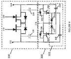
- Fig. 4 illustrates a complete circuit schematic of the circuit that includes the bidirectional switch 100 and the substrate voltage control circuit 300.
- the substrate voltage control circuit 300 includes first and second switching devices 302, 304.
- the first switching device 302 is connected between the substrate region 114 and the first input-output terminal 122.
- the second switching device 304 is connected between the substrate region 114 and the second input-output terminal 124.
- a conductive electrical connection is provided between the substrate region 114 and the second input-output terminal 124.
- the first and second switching devices 302, 304 can be any of a wide variety of electronic switching devices that are configured to complete or remove an electrical connection in response to a control signal.
- Exemplary switching devices include metal-oxide semiconductor field effect transistors (MOSFETs), insulated gate bipolar transistors (IGBTs), bipolar junction transistors (BJTs), junction field effect transistors (JFETs), high electron mobility transistors (HEMTs), etc.
- the first and second switching devices 302, 304 can be formed in a wide variety of semiconductor technologies including type IV semiconductor technology, e.g., Silicon (Si), Silicon carbide (SiC), Silicon germanium (SiGe) etc., and type III-V semiconductor technology, III-V semiconductor technology, e.g., gallium nitride (GaN), gallium arsenide (GaAs), etc.
- type IV semiconductor technology e.g., Silicon (Si), Silicon carbide (SiC), Silicon germanium (SiGe) etc.
- type III-V semiconductor technology III-V semiconductor technology, e.g., gallium nitride (GaN), gallium arsenide (GaAs), etc.
- the first and second switching devices 302, 304 can be voltage controlled switching devices. That is, the first and second switching devices 302, 304 can provide an electrically conductive connection by applying a voltage difference 136 between a control terminal (e.g., the gate) and a reference terminal (e.g., the source) of the device.
- the first and second switching devices 302, 304 can be current controlled switching devices. That is, the conductive electrically connection is achieved by injecting current into the control terminal of the device.
- each of the first and second switching devices 302, 304 may include a reverse conducting diode 306 that is connected antiparallel to the conduction path of the switching device.
- This reverse conducting diode 306 may be inherent to the structure of the switching device 302 and 304.
- the body diode that intrinsically arises at the p-n junction between the body and source regions can provide this reverse conducting diode 306.
- the reverse conducting diode 306 may be separately incorporated into the device.
- the first and second switching devices 302, 304 are integrated into the same semiconductor body 102 as the bidirectional switch 100. That is, the first and second switching devices 302, 304 and the bidirectional switch 100 form a single integrated circuit. Depending on the technology employed, the first and second switching devices 302, 304 can be provided directly beneath the upper active region 104. Alternatively, the first and second switching devices 302, 304 can be formed in region of the semiconductor body 102 (not shown) that is laterally adjacent to the bidirectional switch 100. In one particular embodiment, the bidirectional switch 100 is a type III-V semiconductor device (as shown in the figure) and the first and second switching devices 302, 304 are also type III-V semiconductor devices that are incorporated into the same semiconductor body 102.
- the first and second switching devices 302, 304 can be GaN based HEMTs devices that are incorporated into the same substrate as a GaN based bidirectional switch 100.
- the first and second switching devices 302, 304 are configured as current controlled switches. This configuration can be achieved by configuring the gate structures of the first and second switching devices 302, 304 to inject current into the channel of the device.
- the first and second switching devices 302, 304 can be provided by discrete components that are separate from the semiconductor body 102.
- the substrate voltage control circuit 300 additionally includes a passive electrical network 301 (identified in Fig. 4 ) that is connected to the control terminals of the first and second switching devices 302, 304, the substrate region 114, and the first and second input-output terminals 122, 124.
- the passive electrical network 301 can include any of a wide variety of passive electrical components such as resistors, capacitors, inductors, etc.
- a passive electrical component refers to any electrical component that provides a known IV response that is not controlled by an independent signal.
- the passive electrical network 301 includes a first capacitance 308 that is connected between the control terminal of the second switching device 304 and the first input-output terminal 122 and a second capacitance 310 that is connected between the control terminal of the first switching device 302 and the second input-output terminal 124.
- the first and second capacitances 308, 310 can be provided using a variety of different techniques and structures.
- the first and second capacitances 308, 310 can be provided by a parallel-plate capacitor structure that is specifically designed as such.
- the first and second capacitances 308, 310 can be provided from the parasitic capacitance of a variety of different structures, e.g., wire connections, transistor devices, etc. that are not necessarily designed exclusively to provide the behavior of a capacitor. In either case, these structures can be integrated into the same semiconductor body 102 as the bidirectional switch 100 in a different region (not shown) and electrically connected using known interconnect techniques.
- the first and second capacitances 308, 310 can be provided by discrete devices that are external to the semiconductor body 102.
- the passive electrical network 301 can additionally include a first voltage limiting element 312 connected between the substrate region 114 and the control terminal of the first switching device 302.
- the first voltage limiting element 312 is configured to limit an input voltage applied to the first switching device 302 to below a maximum rated input voltage of the first switching device 302.
- the maximum rated input voltage corresponds to a value that the first switching device 302 can accommodate without failure.
- the first voltage limiting element 312 blocks any voltage below the maximum rated input voltage, and begins conducting once the maximum rated input voltage is reached.
- the first voltage limiting element 312 is a Zener diode, wherein the reverse conducting Zener voltage corresponds to the maximum rated input voltage of the first switching device 302.
- the first voltage limiting element 312 can be any kind of voltage limiting device (e.g., Schottky diode, PIN diode, MOV, etc.) that provides similar functionality.
- the passive electrical network 301 additionally includes a second voltage limiting element 314 connected between the substrate region 114 and an input of the first switching device 302.
- the second voltage limiting element 314 is configured to limit a voltage applied to the control terminal of the second switching device 304 to below a maximum rated input voltage of the second switching device 304 in a similar manner as previously described with reference to the first voltage limiting element 312.
- the second voltage limiting element 314 can be a Zener diode, wherein the reverse conducting Zener voltage corresponds to the maximum rated input voltage of the second switching device 304.
- the second voltage limiting element 314 can be any kind of voltage limiting device (e.g., Schottky diode, PIN diode, MOV, etc.) that provides similar functionality.
- the passive electrical network 301 of the substrate voltage control circuit 300 is configured to operate the first and second switching devices 302, 304 in such a way that alleviates the trapped charges condition as described with reference to Fig. 2B .
- the passive electrical network 301 is configured to generate the necessary control signaling to turn the first and second switching devices 302, 304 ON and OFF without any external or independent signaling. Instead, the control signaling is derived from the voltages that are applied across the first and second input-output terminals 122, 124.
- the passive electrical network 301 In a first transitional state of the bidirectional switch 100 at which the second input-output terminal 124 is at a higher potential than the first input-output terminal 122 and the bidirectional switch 100 is transitioned from OFF to ON (i.e., the condition described with reference to Fig. 1 ), the passive electrical network 301 generates a first substrate reference signal that, at least temporality, turns the second switching device 304 ON. As a result, a short circuit path exists for the charges stored in the first and second substrate capacitances 128, 130 to dissipate.
- the passive electrical network 301 In a second transitional state of the bidirectional switch 100 at which the first input-output terminal 122 is at a second potential than the first input-output terminal 122 and the bidirectional switch 100 is transitioned from OFF to ON, the passive electrical network 301 generates a second substrate reference signal that, at least temporality, turns the first switching device 302 ON. Again, this creates short circuit path that allows the charges stored in the first and second substrate capacitances 128, 130 to dissipate.
- FIG. 5-8 A working example of how the passive electrical network 301 generates the first substrate reference signal during the first transitional state will now be discussed with reference to Figs. 5-8 .
- FIGs. 5-8 Each of these figures contain a complete circuit schematic of the circuit that includes the bidirectional switch 100 and the substrate voltage control circuit 300.
- the bidirectional switch 100 is in an OFF state and can maintain a voltage difference across the first and second input-output terminals 122, 124.
- a voltage difference is applied to the input-output terminals such that the second input-output terminal 124 as at a higher potential than the first input-output terminal 122.
- a voltage difference of 400 V will be used. This 400V is applied across the voltage divider network formed by the first and second substrate capacitances 128, 130 and the substrate voltage control circuit 300.
- the voltage across the gate and reference terminal of the first switching device 302 is slightly below the threshold voltage of the gate diode of the first switching device 302. Thus, the first switching device 302 is turned OFF. Because the first switching device 302 has a reverse conducting diode 306 that is forward conducting at this bias polarity, the voltage across the first substrate capacitance 128 corresponds to the forward conducting voltage (i.e., the forward threshold voltage) of the reverse conducting diode 306 of the first switching device 302. As an example, this voltage is 1 V. The remaining 399 V is applied across the second substrate capacitance 130. In addition, this voltage is applied across the second capacitance 310 and the second switching device 304, which are in parallel with the second substrate capacitance 130. In other words, the substrate voltage control circuit 300 produces a voltage divider condition similar to that described with reference to Fig. 2A .
- the bidirectional switch 100 is transitioned from OFF to ON after being in the previous bias condition described with reference to Fig. 5 .
- This transition occurs by applying the necessary signals to turn the first and second gate structures 118, 120 ON.
- a low resistance connection forms between the first and second input-output terminals 122, 124 and the voltage across the first and second input-output terminals 124 drops from 400V to approximately 0V.
- the charges stored in the first substrate capacitance 128 and the second capacitance 310 redistribute throughout the circuit via the channel 110. In particular, this redistribution of charges occurs causes the first capacitance 308 to charge.
- this first capacitance 308 results in a temporary current being present at the control terminal of the second switching device 304. Because the second switching device 304 is a current controlled switch, this current is sufficient to temporarily place the second switching device 304 in an ON state. Once the second switching device 304 is turned ON, it provides a short circuit path for the charges stored in the first and second substrate capacitances 128, 130 as well as other associated capacitances in the reverse conducting diode 306 and t the second capacitance 310 to dissipate via the first and second input-output terminals 122, 124. Thus, different to the scenario described with reference to Fig. 2B in which the charges stored across the first and second substrate capacitances 128, 130 are blocked by the first and second diodes 132, 134, the second switching device 304 provides an alternate path for these charges to discharge.
- a steady ON state of the bidirectional switch 100 is depicted.
- the control terminal voltage of the first switching device 302 is practically at zero volts and the control terminal of the second switching device 304 is below its threshold voltage.
- the second switching device 304 is controlled by a temporary current provided by the first capacitance 308, the second switching device 304 was only in the ON state temporarily while the bidirectional switch 100 transitions from OFF to ON. Once the first capacitance 308 is no longer charging, the current at the control terminal of the second switching device 304 will subside and the second switching device 304 will automatically turn off.
- the temporary ON state condition of the second switching device 304 may not necessarily discharge all charges stored in the first and second substrate capacitances 128, 130.
- a minimal voltage e.g., 15V or less
- these voltages are low enough to effectively eliminate the problems of the fully charged voltage divider condition described with reference to Fig. 2B .
- the amount of remaining charges stored (and hence voltage) on the first and second substrate capacitances 128, 130 after the second switching device 304 is turned OFF can be tuned by altering device parameters of the substrate voltage control circuit 300 such as, capacitance of the first capacitance 308, on-resistance of the second switching device 304, turn-on behavior of the second switching device 304, etc.
- the bidirectional switch 100 is transitioned from the ON state to the OFF state by turning the first gate structure 118 OFF.
- the channel 110 of the device is now non-conductive.
- the majority of the voltage applied to the first and second input-output terminals 122, 124 is now distributed across the second substrate capacitance 130, the second capacitance 310 and the second switching device 304.
- charging the second capacitance 310 which is in series with the control terminal of the first switching device 302
- the voltage distribution will ultimately revert to the state described with reference to Fig. 5 .
- the previously described second substrate reference signal is generated during the second transitional state, i.e., wherein the first input-output terminal 124 is at a higher potential than the second input-output terminal 122 and the bidirectional switch 100 is transitioned from OFF to ON, in a corresponding manner using counterpart components of the substrate voltage control circuit 300.
- the majority of the voltage difference between the first and second input-output terminals 122, 124 (399 V using the exemplary values described above) is initially placed across the first substrate capacitance 130. This redistribution of charges results in a temporary current at the control terminal of the first switching device 302 to alleviate the blocking voltage divider condition in a similar manner as previously described.
- HEMT is also commonly referred to as HFET (heterostructure field effect transistor), MODFET (modulation-doped FET) and MESFET (metal semiconductor field effect transistor).
- HFET heterostructure field effect transistor
- MODFET modulation-doped FET
- MESFET metal semiconductor field effect transistor
- III-nitride based compound semiconductor transistor incorporating a junction between two materials with different band gaps (i.e., a heterojunction) as the channel.
- GaN may be combined with AlGaN or InGaN to form an electron gas inversion region as the channel.
- the compound semiconductor device may have AlInN/AlN/GaN barrier/spacer/buffer layer structures.
- the normally-off compound semiconductor transistor can be realized using any suitable III-nitride technology such as GaN that permits the formation of opposite polarity inversion regions due to piezoelectric effects.
- the presence of polarization charges and strain effects in a GaN-based heterostructure body due to piezoelectric effects yield a two-dimensional charge carrier gas in the heterostructure body characterized by very high carrier density and carrier mobility.
- a two-dimensional charge carrier gas such as a 2DEG (two-dimensional electron gas) or 2DHG (two-dimensional hole gas)
- a thin, e.g. 1-2nm, AlN layer can be provided between the GaN buffer region and the GaN alloy barrier region to minimize alloy scattering and enhance 2DEG mobility.
- the compound semiconductor transistors described herein can be formed from any binary, ternary or quaternary III-nitride compound semiconductor material where piezoelectric effects are responsible for the device concept.
Landscapes
- Electronic Switches (AREA)
Abstract
Description
- The instant application generally relates to semiconductor devices, and more particularly relates to bidirectional high electron mobility transistors.
- Semiconductor transistors, in particular field-effect controlled switching devices such as a MISFET (Metal Insulator Semiconductor Field Effect Transistor), in the following also referred to as MOSFET (Metal Oxide Semiconductor Field Effect Transistor) and a HEMT (high-electron-mobility Field Effect Transistor) also known as heterostructure FET (HFET) and modulation-doped FET (MODFET) are used in a variety of applications. An HEMT is a transistor with a junction between two materials having different band gaps, such as GaN and AlGaN.
- HEMTs are viewed as an attractive candidate for power transistor applications, i.e., applications in which switching of substantially large voltages and/or currents is required. HEMTs offer high conduction and low resistive losses in comparison to conventional silicon based devices.
- HEMTs are commonly formed from III-V semiconductor materials, such as GaN, GaAs, InGaN, AlGaN, etc. In a GaN/AlGaN based HEMT, a two-dimensional electron gas (2DEG) arises at the interface between the AlGaN barrier layer and the GaN buffer layer. The 2DEG forms the channel of the device instead of a doped region, which forms the channel in a conventional MOSFET device. Similar principles may be utilized to select buffer and barrier layers that form a two-dimensional hole gas (2DHG) as the channel of the device. A 2DEG or a 2DHG is generally referred to as a two-dimensional carrier gas. Without further measures, the heterojunction configuration leads to a self-conducting, i.e., normally-on, transistor. Normally-off structures are also possible. In these cases, measures must be taken to prevent the channel region of an HEMT from being in a conductive state in the absence of a positive gate voltage.
- One application of type III-V semiconductor technology is a bidirectional switch. A bidirectional switch is a device that is capable of switching voltages of positive or negative polarity. That is, a bidirectional switch is configured to control current flow in both directions. A dual gate type III-V semiconductor bidirectional switch can be realized by providing two HEMT gate structures in series between two electrically conductive terminals that are in contact with the two-dimensional carrier gas. The two HEMTs can share the same drift region (the resistive voltage sustaining part) of the device which means the on-state resistance can be approximately half of a conventional back to back device.
- One problem associated with bidirectional switches relates to capacitive coupling between the channel of the device and the underlying semiconductor substrate. In conventional unidirectional semiconductor switching devices, the underlying semiconductor substrate is typically tied to the reference potential terminal (e.g., the source terminal) of the device by substrate contacts. By tying the substrate to a fixed potential, the problem of capacitive coupling between a floating substrate and the channel is eliminated and hence the reliability and stability of the device operation is improved. The same benefit cannot be obtained using a simple electrical contact in the case of a bidirectional switch because there is not a single terminal that is maintained at a reference potential in all states of operations; the voltage polarity across the device changes. Known solutions to this problem suffer from various drawbacks.
- A semiconductor device is disclosed. According to an embodiment, the semiconductor device includes a semiconductor body having an active region and a substrate region that is disposed beneath the active region. A bidirectional switch is formed in the semiconductor body and is configured to block voltage across two polarities. The bidirectional switch includes first and second gate structures that are each configured to control a conductive state of an electrically conductive channel that is disposed in the upper active region, and first and second input-output terminals that are each in ohmic contact with the electrically conductive channel. A first switching device is configured to electrically connect the substrate region to the first input-output terminal. A second switching device is configured to electrically connect the substrate region to the second input- output terminal. A passive electrical network includes a first capacitance and a second capacitance. The first capacitance is connected between a control terminal of the second switching device and the first input-output terminal. The second capacitance is connected between a control terminal of the first switching device and the second input-output terminal. The passive electrical network is configured to temporarily electrically connect the substrate region to the second input-output terminal by turning the second switching device on when the second input-output terminal is at a higher potential than the first input-output terminal. The passive electrical network is configured to temporarily electrically connect the substrate region to the first input-output terminal by turning the first switching device on when the first input-output terminal is at a higher potential than the second input-output terminal.
- In some embodiments, the first and second switching devices are current controlled switches, wherein the first capacitance is configured to supply a temporary current to the control terminal of the second switching device during a transition of the bidirectional switch from a blocking state to a conducting state at a first voltage polarity of the bidirectional switch, and wherein the second capacitance is configured to supply a temporary current to the control terminal of the first switching device during a transition of the bidirectional switch from a blocking state to a conducting state at a second voltage polarity of the bidirectional switch, the second voltage polarity being opposite from the first voltage polarity.
- In some embodiments, the semiconductor body comprises a type III semiconductor nitride, wherein the bidirectional switch is a high electron mobility transistor, and wherein the electrically conductive channel is a two-dimensional charge carrier gas.
- lin some embodiments, the first and second switching devices are high-electron-mobility transistors that are integrally formed in the semiconductor body.
- In some embodiments, the first capacitance is exclusively connected between the control terminal of the second switching device and the first input-output terminal, and wherein the second capacitance is exclusively connected between the control terminal of the first switching device and the second input-output terminal.
- In some embodiments, the passive electrical network further comprises a first voltage limiting element connected between the substrate region and an input of the first switching device, a second voltage limiting element connected between the substrate region and an input of the first switching device, wherein the first voltage limiting element is configured to limit a voltage applied to the control terminal of the first switching device to below a maximum rated input voltage of the first switching device, and wherein the second voltage limiting element is configured to limit a voltage applied to the control terminal of the second switching device to below a maximum rated input voltage of the second switching device.
- In some embodiments, the first and second switching devices are integrated within the semiconductor body.
- In some embodiments, the passive electrical network is integrated within the semiconductor body and is exclusively connected to the first and second input-output terminals, the first and second switching devices and the substrate region.
- According to another embodiment, the semiconductor device includes a semiconductor body having an active region and a substrate region that is disposed beneath the active region. A bidirectional switch is formed in the semiconductor body and is configured to block voltage across two polarities. The bidirectional switch includes first and second gate structures that are each configured to control a conductive state of an electrically conductive channel that is disposed in the upper active region, and first and second input-output terminals that are each in ohmic contact with the electrically conductive channel. A first switching device is configured to electrically connect the substrate region to the first input-output terminal when turned on. A second switching device is configured to electrically connect the substrate region to the second input-output terminal when turned on. A passive electrical network is configured to generate a first substrate reference signal that turns the second switching device on during a first transitional state of the bidirectional switch and to generate a second substrate reference signal that turns the first switching device on during a second transitional state of the bidirectional switch. The first transitional state is a state when the second input-output terminal is at a higher potential than the first input-output terminal and the bidirectional switch is turned on, the second transitional state is a state when the first input-output terminal is at a higher potential than the second input-output terminal and the bidirectional switch is turned on.
- In some embodiments, the self-biasing passive electrical network comprises a first capacitance and a second capacitance, the first capacitance being connected between a control terminal of the second switching device and the first input-output terminal, the second capacitance being connected between a control terminal of the first switching device and the second input-output terminal, wherein the first capacitance is configured to provide the first substrate reference signal during the first transitional state, and wherein the second capacitance is configured to provide the second substrate reference signal during the second transitional state.
- In some embodiments, the first and second switching devices are current controlled switches, wherein the self-biasing passive electrical network is configured to generate the first substrate reference signal by providing a temporary current pulse at the control terminal of the second switching device from a redistribution of charges occurring during the first transitional state, and wherein the self-biasing passive electrical network is configured to generate the second substrate reference signal by providing a temporary current pulse at the control terminal of the first switching device from a redistribution of charges occurring during the second transitional state.
- In some embodiments, the semiconductor body comprises a type III semiconductor nitride, wherein the bidirectional switch is a high electron mobility transistor, and wherein the electrically conductive channel is a two-dimensional charge carrier gas.
- In some embodiments, the first and second switching devices are high-electron-mobility transistors that are integrally formed in the semiconductor body.
- In some embodiments, the first capacitance is exclusively connected between the control terminal of the second switching device and the first input-output terminal, and wherein the second capacitance is exclusively connected between the control terminal of the first switching device and the second input-output terminal.
- A method of operating a bidirectional switch is disclosed. The bidirectional switch is configured to block voltage across two polarities. The bidirectional switch includes a semiconductor body having an active region and a substrate region that is disposed beneath the active region, first and second gate structures that are each configured to control a conductive state of an electrically conductive channel that is disposed in the upper active region, and first and second input-output terminals that are each in ohmic contact with the electrically conductive channel. According to an embodiment of the method, the second switching device is used to temporarily electrically connect the substrate region to the second input-output terminal during a first transitional state of the bidirectional switch. The first transitional state of the bidirectional switch is a state when the second input-output terminal is at a higher potential than the first input-output terminal and the bidirectional switch is transitioned from OFF to ON. A first switching device is used to temporarily electrically connect the substrate region to the first input-output terminal during a second transitional state of the bidirectional switch. The second transitional state of the bidirectional switch is a state when the first input-output terminal is at a higher potential than the second input-output terminal and the bidirectional switch is transitioned from OFF to ON. Using the first switching device and using the second switching device includes turning the first and second switching devices on using a passive electrical network that that generates a current pulse from transitioning of the bidirectional switch.
- In some embodiments, the self-biasing passive electrical network comprises a first capacitance and a second capacitance, the first capacitance being connected between a control terminal of the second switching device and the first input-output terminal, the second capacitance being connected between a control terminal of the first switching device and the second input-output terminal.
- In some embodiments, the self-biasing passive electrical network provides a first temporary current pulse at the control terminal of the second switching device during the during the first transitional state, and wherein the self-biasing passive electrical network provides a second temporary current pulse at the control terminal of the first switching device during the during the second transitional state.
- In some embodiments, the first capacitance generates the first temporary current pulse from a redistribution of charges that occurs in the bidirectional switch during the first transitional state, and wherein the second capacitance generates the second temporary current pulse from a redistribution of charges that occurs in the bidirectional switch during the second transitional state.
- In some embodiments, the bidirectional switch, the first switching device and the second switching device are integrally formed in the semiconductor body, and wherein the self-biasing passive electrical network turns the first and second switching devices ON exclusively using voltages supplied to the first and second input-output terminals.
- The elements of the drawings are not necessarily to scale relative to each other. Like reference numerals designate corresponding similar parts. The features of the various illustrated embodiments can be combined unless they exclude each other. Embodiments are depicted in the drawings and are detailed in the description which follows.
-
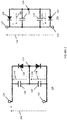
Figure 1 illustrates a bidirectional switch with a network of diodes connected between the input-output terminals of the bidirectional switch and the substrate region of the bidirectional switch, according to an embodiment. -
Figure 2 , which includesFigs. 2A and 2B , illustrates equivalent circuit schematics of the bidirectional switch in two different operational states, according to an embodiment.Fig. 2A depicts the bidirectional switch in an OFF state.Fig. 2A depicts the bidirectional switch in an ON state. -
Figure 3 illustrates a bidirectional switch with a substrate voltage regulation circuit connected between the input-output terminals of the bidirectional switch and the substrate region of the bidirectional switch, according to an embodiment. -
Figure 4 illustrates an equivalent circuit schematic of a bidirectional switch with a substrate voltage regulation circuit connected between the input-output terminals of the bidirectional switch and the substrate region of the bidirectional switch, according to an embodiment. -
Figure 5 illustrates the various voltages present on the bidirectional switch and the substrate voltage regulation circuit during a steady OFF state of the bidirectional switch, according to an embodiment. -
Figure 6 illustrates the various voltages present on the bidirectional switch and the substrate voltage regulation circuit during a transitional state of the bidirectional switch from OFF to ON, according to an embodiment. -
Figure 7 illustrates the various voltages present on the bidirectional switch and the substrate voltage regulation circuit during a steady ON state of the bidirectional switch, according to an embodiment. -
Figure 8 illustrates the various voltages present on the bidirectional switch and the substrate voltage regulation circuit during a transitional state of the bidirectional switch from OFF to ON, according to an embodiment. - According to embodiments described herein, a bidirectional switch is disclosed with substrate voltage regulation circuit connected between the input-output terminals of the bidirectional switch and the substrate region of the bidirectional switch. The bidirectional switch includes switching devices (e.g., transistors) that are configured to connect the input-output terminals of the bidirectional switch to a substrate region, depending upon the operational state of the bidirectional switch. If the bidirectional switch is operating at a first voltage polarity wherein a second input-output terminal is at a higher potential than a first input-output terminal and is transitioned from OFF to ON, a first switching device electrically connects the substrate region to the second input-output terminal. If the bidirectional switch is operating at a second voltage polarity wherein the first input-output terminal is at a higher potential than the second input-output terminal and is transitioned from OFF to ON, a second switching device electrically connects the substrate region to the first input-output terminal.
- Advantageously, the bidirectional switch includes a passive electrical network that can provide the necessary control signaling to turn the first and second switching devices ON and OFF without any independent biasing or control signals. That is, the passive electrical network is self-biasing in the sense that it utilizes the same voltages that are applied across the input-output terminals of the bidirectional switch to generate the control signaling for the first and second switching devices. In one particular example, the passive electrical network includes capacitors that are connected in series with the control terminals of current driven switches. The transition from OFF to ON of the bidirectional switch results in a temporary redistribution of charges across the capacitor network that causes a current pulse to appear at the control terminal of the appropriate switching device. Advantageously, this solution can be integrated into a single integrated circuit. For example, a GaN based bidirectional switch can be combined with GaN based current driven switching devices and integrally formed capacitances to provide the complete circuit. This provides a simpler and more cost effective solution in comparison to a technique that utilizes discrete components and external biasing signals to provide similar functionality.
- Referring to
Fig. 1 , abidirectional switch 100 is depicted, according to an embodiment. Thebidirectional switch 100 is formed in asemiconductor body 102. Generally speaking, thesemiconductor body 102 region can include a wide variety of semiconductor materials including group IV semiconductor materials such as Silicon (Si), compound group IV semiconductor materials such as Silicon carbide (SiC) or Silicon germanium (SiGe), and group III-V semiconductor materials such as gallium nitride (GaN), aluminum gallium nitride (AlGaN), indium gallium nitride (InGaN), gallium arsenide (GaAs), aluminum gallium arsenide (AlGaAs), as well as isolation materials such as sapphire, etc. - A top portion of the
semiconductor body 102 includes an upperactive region 104. The upperactive region 104 refers to the layers or regions of thesemiconductor body 102 that provide an electrically conductive channel. For example, in the depicted embodiment, the upperactive region 104 includes first and second type III-V semiconductor layers 106, 108. The second type III-V semiconductor layer 108 is formed from a semiconductor material having a different band gap than the first type III-V semiconductor layer 106. For example, the first type III-V semiconductor layer 106 can include intrinsic or lightly doped gallium nitride (GaN) and the second type III-V semiconductor layer 108 include aluminum gallium nitride (AlGaN). More generally, any combination of type III-V semiconductor materials with different metallic contents can be used to provide a difference in bandgap. Due to the difference in bandgap between the first and second type III-V semiconductor layers 106, 108, an electrically conductive two-dimensional chargecarrier gas channel 110 arises near an interface between the first type III-V semiconductor layer 106 and the second type III-V semiconductor layer 108 due to polarization effects. Alternatively, instead of type III-V semiconductor material, the upperactive region 104 can include group IV semiconductor materials such as Silicon (Si), Silicon carbide (SiC), Silicon germanium (SiGe), etc. The materials can be doped to form active device regions, e.g., source, drain, collector, emitter, etc., which provide a controllable electrically conductive channel in a known manner. - A
lower portion 112 of thesemiconductor body 102 includes various regions of thesemiconductor body 102 that do not directly contribute in an electrical sense to the provision of the electricallyconductive channel 110. In the depicted embodiment, thelower portion 112 of thesemiconductor body 102 includes asubstrate region 114, anucleation layer 116, and alattice transition region 117. Thesubstrate region 114 can include can be formed from group IV or group III-V semiconductor materials. For example, according to one embodiment, thesubstrate region 114 can be provided by a silicon or silicon based wafer. Thenucleation layer 116, which may include a metal nitride (e.g., AlN), and thelattice transition region 117, which may include a number of semiconductor nitride (e.g., AlGaN) layers with a gradually diminishing metallic content, are provided on thesubstrate region 114 to enable the formation of relatively strain and defect free group IV semiconductor material thereon. More generally, thesubstrate region 114 can include any intrinsic or bulk portion of the substrate that is beneath the active device regions, and is more conductive than an intermediary region that is between thesubstrate region 114 and the upperactive region 104. - The bidirectional switch additionally includes first and
second gate structures semiconductor body 102. The first andsecond gate structures conductive gate electrode 122,semiconductor body 102. According to one embodiment, theintermediary regions 124 are configured (e.g., by doping) to provide an integrated diode in the gate structure. In the case of a type III-V semiconductor device, the first andsecond gate structures semiconductor body 102. - The
bidirectional switch 100 additionally includes first and second input-output terminals channel 110. The ohmic connection can be provided by electricallyconductive contact structures 126 that are formed in thesemiconductor body 102. Thesecontact structures 126 can be formed from conductive metals, such as tungsten or aluminum, or alternatively can be formed from highly-doped monocrystalline or polycrystalline semiconductors. - The
bidirectional switch 100 operates as follows. At a first voltage polarity, in which the second input-output terminal 124 is at a higher voltage than the first input-output terminal 122, voltage blocking is primarily handled by thefirst gate structure 118. That is, an "OFF" signal applied to the first gate structure 118 (e.g., 0V, relative to the first input-output terminal 122) will disrupt thechannel 110 and causes the device to be in a blocking mode. Thebidirectional switch 100 becomes conductive by applying an "ON" signal (e.g., a positive voltage, relative to the first input-output terminal 122) to thefirst gate structure 118, which places thechannel 110 in a conductive state. At a second voltage polarity, in which the first input-output terminal 122 is at a higher voltage than the second input-output terminal 124, the opposite applies. That is, voltage blocking is primarily handled by thesecond gate structure 120. In this way, thebidirectional switch 100 can block or permit a current to flow in either direction between the first and second input-output terminals bidirectional switch 100 can have symmetrical voltage blocking capability at either voltage polarity. Alternatively, thebidirectional switch 100 can be configured to have a greater voltage blocking capability at one of the two voltage polarities. This can be achieved by, among other things, adjusting the distance between the first andsecond gate structures output terminals - One problem associated with
bidirectional switch 100 that are integrated into a single substrate, as is the case in the device ofFig. 1 , is the so-called "common substrate" problem. In the absence of any further measures, there is a parasitic capacitive coupling that occurs between the first and second input-output terminals substrate region 114. In the figure, afirst substrate capacitance 128 represents the parasitic capacitance between the first input-output terminal 122 and thesubstrate region 114, and asecond substrate capacitance 130 represents the parasitic capacitance between the second input-output terminal 124 and thesubstrate region 114. If thesubstrate region 114 is not tied to a fixed potential, the voltages across these parasitic capacitances can vary during the operation of the device, which may degrade the channel and affect the switching behavior during operation of thebidirectional switch 100. In a conventional unidirectional device, this problem is typically solved by tying the substrate of the device to the same potential as the reference potential terminal (e.g., the source terminal) and thus shunting the parasitic substrate capacitance. However, this solution is not available in a bidirectional device because there is no dedicated reference potential terminal. That is, the first input-output terminal 122 acts as a reference potential at one voltage polarity and the second input-output terminal 124 acts as a reference potential at the opposite voltage polarity. - The semiconductor device depicted in
Fig. 1 additionally includes a network of first andsecond diodes second diodes Fig. 1 . In principle, these diodes can be integrally formed in thesemiconductor body 102 and electrically connected in the depicted manner using known interconnect techniques. Alternatively, these diodes can be provided using discrete devices that are separate from thebidirectional switch 100. The anode of thefirst diode 132 is connected to thesubstrate region 114 and the cathode of thefirst diode 132 is connected to the first input-output terminal 122. The anode of thesecond diode 134 is connected to thesubstrate region 114 and the cathode of thesecond diode 134 is connected to the second input-output terminal 124. - Referring to
Fig. 2 , equivalent schematics of thebidirectional switch 100 and the network of first andsecond diodes bidirectional switch 100.Fig. 2A depicts an equivalent schematic when thebidirectional switch 100 is in an OFF state and the second input-output terminal 124 is at a higher potential than the first input-output terminal 122. For exemplary purposes of discussion, avoltage difference 136 of 200V will be used.Fig. 2B depicts an equivalent schematic when thebidirectional switch 100 is transitioned to an ON state after the operational state ofFig. 2A . - Referring to
Fig. 2A , because thebidirectional switch 100 is turned OFF, the connection between the first and second input-output terminals voltage difference 136 between the first and second input-output terminals second substrate capacitances second diode first diode 132 is in forward conducting mode. Thevoltage 138 across thefirst substrate capacitance 128 corresponds to the forward threshold voltage of thefirst diode 132, and is therefore very small (e.g., about 1V). Thevoltage 140 across thesecond substrate capacitance 130 corresponds to the remaining voltage difference between the first and second input-output terminals second diodes output terminal 122 to the substrate potential, and maintains the entireapplied voltage difference 136 between the second input-output terminal 124 and thesubstrate region 114. This condition is desirable, as it effectively mimics the effect of a substrate contact (minus the forward voltage of one diode) in a unidirectional device. - Referring to
Fig 2B , because thebidirectional switch 100 is turned ON, a conductive connection between the first and second input-output terminals voltage difference 136 between the first and second input-output terminal 124 changes to 0V. Moreover, this connection reconfigures the voltage divider network that includes the first andsecond substrate capacitances second diodes second substrate capacitances second diodes second substrate capacitances second diodes second substrate capacitances output terminals second substrate capacitances voltage 138 across thefirst substrate capacitance 128 corresponds to roughly half of the previous voltage difference 136 (e.g., about 99V) and thevoltage 140 across thesecond substrate capacitance 130 corresponds to roughly half of the previous voltage difference 136 (e.g., about 99V). - Thus, while the network of first and
second diodes Fig. 1 provides desirable substrate shunting behavior in the OFF state of thebidirectional switch 100, the transition from OFF to ON creates an undesirable condition in which the previously applied voltage is shared across the voltage divider that includes the first andsecond substrate capacitances - Referring to
Figs. 3 and4 , a semiconductor device is depicted, according to another embodiment. The semiconductor device includes thebidirectional switch 100 that is formed in thesemiconductor body 102 as described with reference toFig. 1 . Different to the embodiment ofFig. 1 , the first andsecond diodes voltage control circuit 300.Fig. 3 illustrates a substrate configuration of thebidirectional switch 100 with the substratevoltage control circuit 300 being schematically depicted.Fig. 4 illustrates a complete circuit schematic of the circuit that includes thebidirectional switch 100 and the substratevoltage control circuit 300. - The substrate
voltage control circuit 300 includes first andsecond switching devices first switching device 302 is connected between thesubstrate region 114 and the first input-output terminal 122. Thus, by turning thefirst switching device 302 ON, a conductive electrical connection is provided between thesubstrate region 114 and the first input-output terminal 122. Likewise, thesecond switching device 304 is connected between thesubstrate region 114 and the second input-output terminal 124. Thus, by turning thesecond switching device 304 ON, a conductive electrical connection is provided between thesubstrate region 114 and the second input-output terminal 124. - The first and
second switching devices second switching devices - The first and
second switching devices second switching devices voltage difference 136 between a control terminal (e.g., the gate) and a reference terminal (e.g., the source) of the device. Alternatively, the first andsecond switching devices - As can be seen, each of the first and
second switching devices reverse conducting diode 306 that is connected antiparallel to the conduction path of the switching device. Thisreverse conducting diode 306 may be inherent to the structure of theswitching device reverse conducting diode 306. Alternatively, thereverse conducting diode 306 may be separately incorporated into the device. - According to an embodiment, the first and
second switching devices same semiconductor body 102 as thebidirectional switch 100. That is, the first andsecond switching devices bidirectional switch 100 form a single integrated circuit. Depending on the technology employed, the first andsecond switching devices active region 104. Alternatively, the first andsecond switching devices bidirectional switch 100. In one particular embodiment, thebidirectional switch 100 is a type III-V semiconductor device (as shown in the figure) and the first andsecond switching devices same semiconductor body 102. For example, the first andsecond switching devices bidirectional switch 100. In one more particular embodiment, the first andsecond switching devices second switching devices second switching devices semiconductor body 102. - The substrate
voltage control circuit 300 additionally includes a passive electrical network 301 (identified inFig. 4 ) that is connected to the control terminals of the first andsecond switching devices substrate region 114, and the first and second input-output terminals electrical network 301 can include any of a wide variety of passive electrical components such as resistors, capacitors, inductors, etc. As used herein, a passive electrical component refers to any electrical component that provides a known IV response that is not controlled by an independent signal. - The passive
electrical network 301 includes afirst capacitance 308 that is connected between the control terminal of thesecond switching device 304 and the first input-output terminal 122 and asecond capacitance 310 that is connected between the control terminal of thefirst switching device 302 and the second input-output terminal 124. - The first and
second capacitances second capacitances second capacitances same semiconductor body 102 as thebidirectional switch 100 in a different region (not shown) and electrically connected using known interconnect techniques. Alternatively, the first andsecond capacitances semiconductor body 102. - The passive
electrical network 301 can additionally include a firstvoltage limiting element 312 connected between thesubstrate region 114 and the control terminal of thefirst switching device 302. The firstvoltage limiting element 312 is configured to limit an input voltage applied to thefirst switching device 302 to below a maximum rated input voltage of thefirst switching device 302. The maximum rated input voltage corresponds to a value that thefirst switching device 302 can accommodate without failure. The firstvoltage limiting element 312 blocks any voltage below the maximum rated input voltage, and begins conducting once the maximum rated input voltage is reached. According to an embodiment, the firstvoltage limiting element 312 is a Zener diode, wherein the reverse conducting Zener voltage corresponds to the maximum rated input voltage of thefirst switching device 302. More generally, the firstvoltage limiting element 312 can be any kind of voltage limiting device (e.g., Schottky diode, PIN diode, MOV, etc.) that provides similar functionality. - The passive
electrical network 301 additionally includes a secondvoltage limiting element 314 connected between thesubstrate region 114 and an input of thefirst switching device 302. The secondvoltage limiting element 314 is configured to limit a voltage applied to the control terminal of thesecond switching device 304 to below a maximum rated input voltage of thesecond switching device 304 in a similar manner as previously described with reference to the firstvoltage limiting element 312. Similarly, the secondvoltage limiting element 314 can be a Zener diode, wherein the reverse conducting Zener voltage corresponds to the maximum rated input voltage of thesecond switching device 304. Alternatively, the secondvoltage limiting element 314 can be any kind of voltage limiting device (e.g., Schottky diode, PIN diode, MOV, etc.) that provides similar functionality. - Advantageously, the passive
electrical network 301 of the substratevoltage control circuit 300 is configured to operate the first andsecond switching devices Fig. 2B . Moreover, the passiveelectrical network 301 is configured to generate the necessary control signaling to turn the first andsecond switching devices output terminals - In a first transitional state of the
bidirectional switch 100 at which the second input-output terminal 124 is at a higher potential than the first input-output terminal 122 and thebidirectional switch 100 is transitioned from OFF to ON (i.e., the condition described with reference toFig. 1 ), the passiveelectrical network 301 generates a first substrate reference signal that, at least temporality, turns thesecond switching device 304 ON. As a result, a short circuit path exists for the charges stored in the first andsecond substrate capacitances bidirectional switch 100 at which the first input-output terminal 122 is at a second potential than the first input-output terminal 122 and thebidirectional switch 100 is transitioned from OFF to ON, the passiveelectrical network 301 generates a second substrate reference signal that, at least temporality, turns thefirst switching device 302 ON. Again, this creates short circuit path that allows the charges stored in the first andsecond substrate capacitances - A working example of how the passive
electrical network 301 generates the first substrate reference signal during the first transitional state will now be discussed with reference toFigs. 5-8 . Each of these figures contain a complete circuit schematic of the circuit that includes thebidirectional switch 100 and the substratevoltage control circuit 300. - Referring to
Fig. 5 , thefirst gate structure 118 is turned OFF, and the second gate structure is either ON or OFF. As a result, thebidirectional switch 100 is in an OFF state and can maintain a voltage difference across the first and second input-output terminals output terminal 124 as at a higher potential than the first input-output terminal 122. For the exemplary purposes of discussion, a voltage difference of 400 V will be used. This 400V is applied across the voltage divider network formed by the first andsecond substrate capacitances voltage control circuit 300. The voltage across the gate and reference terminal of thefirst switching device 302 is slightly below the threshold voltage of the gate diode of thefirst switching device 302. Thus, thefirst switching device 302 is turned OFF. Because thefirst switching device 302 has areverse conducting diode 306 that is forward conducting at this bias polarity, the voltage across thefirst substrate capacitance 128 corresponds to the forward conducting voltage (i.e., the forward threshold voltage) of thereverse conducting diode 306 of thefirst switching device 302. As an example, this voltage is 1 V. The remaining 399 V is applied across thesecond substrate capacitance 130. In addition, this voltage is applied across thesecond capacitance 310 and thesecond switching device 304, which are in parallel with thesecond substrate capacitance 130. In other words, the substratevoltage control circuit 300 produces a voltage divider condition similar to that described with reference toFig. 2A . - Referring to
Fig. 6 thebidirectional switch 100 is transitioned from OFF to ON after being in the previous bias condition described with reference toFig. 5 . This transition occurs by applying the necessary signals to turn the first andsecond gate structures output terminals output terminals 124 drops from 400V to approximately 0V. Once this happens, the charges stored in thefirst substrate capacitance 128 and thesecond capacitance 310 redistribute throughout the circuit via thechannel 110. In particular, this redistribution of charges occurs causes thefirst capacitance 308 to charge. The charging of thisfirst capacitance 308 results in a temporary current being present at the control terminal of thesecond switching device 304. Because thesecond switching device 304 is a current controlled switch, this current is sufficient to temporarily place thesecond switching device 304 in an ON state. Once thesecond switching device 304 is turned ON, it provides a short circuit path for the charges stored in the first andsecond substrate capacitances reverse conducting diode 306 and t thesecond capacitance 310 to dissipate via the first and second input-output terminals Fig. 2B in which the charges stored across the first andsecond substrate capacitances second diodes second switching device 304 provides an alternate path for these charges to discharge. - Referring to
Fig. 7 , a steady ON state of thebidirectional switch 100 is depicted. In the steady ON state of thebidirectional switch 100, the control terminal voltage of thefirst switching device 302 is practically at zero volts and the control terminal of thesecond switching device 304 is below its threshold voltage. Because thesecond switching device 304 is controlled by a temporary current provided by thefirst capacitance 308, thesecond switching device 304 was only in the ON state temporarily while thebidirectional switch 100 transitions from OFF to ON. Once thefirst capacitance 308 is no longer charging, the current at the control terminal of thesecond switching device 304 will subside and thesecond switching device 304 will automatically turn off. The temporary ON state condition of thesecond switching device 304 may not necessarily discharge all charges stored in the first andsecond substrate capacitances second substrate capacitances bidirectional switch 100 is operating in the steady ON state. However, these voltages are low enough to effectively eliminate the problems of the fully charged voltage divider condition described with reference toFig. 2B . Moreover, the amount of remaining charges stored (and hence voltage) on the first andsecond substrate capacitances second switching device 304 is turned OFF can be tuned by altering device parameters of the substratevoltage control circuit 300 such as, capacitance of thefirst capacitance 308, on-resistance of thesecond switching device 304, turn-on behavior of thesecond switching device 304, etc. - Referring to
Fig. 8 , thebidirectional switch 100 is transitioned from the ON state to the OFF state by turning thefirst gate structure 118 OFF. Thechannel 110 of the device is now non-conductive. During the transitional period from the ON state to the OFF state, the majority of the voltage applied to the first and second input-output terminals second substrate capacitance 130, thesecond capacitance 310 and thesecond switching device 304. Although charging thesecond capacitance 310, which is in series with the control terminal of thefirst switching device 302, temporarily turns thefirst switching device 302 ON and thus temporarily shorts thefirst substrate capacitance 128, this state will quickly transition to the steady OFF state once the temporary charging current subsides and thefirst switching device 302 turns OFF. As a result, the voltage distribution will ultimately revert to the state described with reference toFig. 5 . - The previously described second substrate reference signal is generated during the second transitional state, i.e., wherein the first input-
output terminal 124 is at a higher potential than the second input-output terminal 122 and thebidirectional switch 100 is transitioned from OFF to ON, in a corresponding manner using counterpart components of the substratevoltage control circuit 300. To summarize, in the second transitional state, the majority of the voltage difference between the first and second input-output terminals 122, 124 (399 V using the exemplary values described above) is initially placed across thefirst substrate capacitance 130. This redistribution of charges results in a temporary current at the control terminal of thefirst switching device 302 to alleviate the blocking voltage divider condition in a similar manner as previously described. - The term HEMT is also commonly referred to as HFET (heterostructure field effect transistor), MODFET (modulation-doped FET) and MESFET (metal semiconductor field effect transistor). The terms HEMT, HFET, MESFET and MODFET are used interchangeably herein to refer to any III-nitride based compound semiconductor transistor incorporating a junction between two materials with different band gaps (i.e., a heterojunction) as the channel. For example, GaN may be combined with AlGaN or InGaN to form an electron gas inversion region as the channel. The compound semiconductor device may have AlInN/AlN/GaN barrier/spacer/buffer layer structures. In general, the normally-off compound semiconductor transistor can be realized using any suitable III-nitride technology such as GaN that permits the formation of opposite polarity inversion regions due to piezoelectric effects.
- Specifically with regard to GaN technology, the presence of polarization charges and strain effects in a GaN-based heterostructure body due to piezoelectric effects yield a two-dimensional charge carrier gas in the heterostructure body characterized by very high carrier density and carrier mobility. Such a two-dimensional charge carrier gas, such as a 2DEG (two-dimensional electron gas) or 2DHG (two-dimensional hole gas), forms the conductive channel of the HEMT near the interface between, e.g., a GaN alloy barrier region and a GaN buffer region. A thin, e.g. 1-2nm, AlN layer can be provided between the GaN buffer region and the GaN alloy barrier region to minimize alloy scattering and enhance 2DEG mobility. In a broad sense, the compound semiconductor transistors described herein can be formed from any binary, ternary or quaternary III-nitride compound semiconductor material where piezoelectric effects are responsible for the device concept.
- Spatially relative terms such as "under," "below," "lower," "over," "upper," "above," "beneath" and the like, are used for ease of description to explain the positioning of one element relative to a second element. These terms are intended to encompass different orientations of the device in addition to different orientations than those depicted in the figures. Further, terms such as "first," "second," and the like, are also used to describe various elements, regions, sections, etc. and are also not intended to be limiting. Like terms refer to like elements throughout the description.
- As used herein, the terms "having," "containing," "including," "comprising" and the like are open-ended terms that indicate the presence of stated elements or features, but do not preclude additional elements or features. The articles "a," "an" and "the" are intended to include the plural as well as the singular, unless the context clearly indicates otherwise.
- Terms such as "same," "match," and "matches" as used herein are intended to mean identical, nearly identical or approximately so that some reasonable amount of variation is contemplated without departing from the spirit of the invention. The term "constant" means not changing or varying, or changing or varying slightly again so that some reasonable amount of variation is contemplated without departing from the spirit of the invention. Further, terms such as "first," "second," and the like are used to describe various elements, regions, sections, etc., and are also not intended to be limiting. Like terms refer to like elements throughout the description.
- It is to be understood that the features of the various embodiments described herein may be combined with each other, unless specifically noted otherwise.
- Although specific embodiments have been illustrated and described herein, it will be appreciated by those of ordinary skill in the art that a variety of alternate and/or equivalent implementations may be substituted for the specific embodiments shown and described without departing from the scope of the present invention. This application is intended to cover any adaptations or variations of the specific embodiments discussed herein. Therefore, it is intended that this invention be limited only by the claims and the equivalents thereof.
Claims (15)
- A semiconductor device, comprising:a semiconductor body comprising an active region and a substrate region that is disposed beneath the active region,a bidirectional switch formed in the semiconductor body and configured to block voltage across two polarities, the bidirectional switch comprising:first and second gate structures that are each configured to control a conductive state of an electrically conductive channel that is disposed in the upper active region, and first and second input-output terminals that are each in ohmic contact with the electrically conductive channel;a first switching device configured to electrically connect the substrate region to the first input-output terminal;a second switching device configured to electrically connect the substrate region to the second input-output terminal;a passive electrical network comprising a first capacitance and a second capacitance, the first capacitance being connected between a control terminal of the second switching device and the first input-output terminal, the second capacitance being connected between a control terminal of the first switching device and the second input-output terminal;wherein the passive electrical network is configured to temporarily electrically connect the substrate region to the second input-output terminal by turning the second switching device on when the second input-output terminal is at a higher potential than the first input-output terminal, andwherein the passive electrical network is configured to temporarily electrically connect the substrate region to the first input-output terminal by turning the first switching device on when the first input-output terminal is at a higher potential than the second input-output terminal.
- The semiconductor device of claim 1, wherein the first and second switching devices are current controlled switches, wherein the first capacitance is configured to supply a temporary current to the control terminal of the second switching device during a transition of the bidirectional switch from a blocking state to a conducting state at a first voltage polarity of the bidirectional switch, and wherein the second capacitance is configured to supply a temporary current to the control terminal of the first switching device during a transition of the bidirectional switch from a blocking state to a conducting state at a second voltage polarity of the bidirectional switch, the second voltage polarity being opposite from the first voltage polarity.
- The semiconductor device of claim 1 or claim 2, wherein the passive electrical network further comprises:a first voltage limiting element connected between the substrate region and an input of the first switching device;a second voltage limiting element connected between the substrate region and an input of the first switching device;wherein the first voltage limiting element is configured to limit a voltage applied to the control terminal of the first switching device to below a maximum rated input voltage of the first switching device, andwherein the second voltage limiting element is configured to limit a voltage applied to the control terminal of the second switching device to below a maximum rated input voltage of the second switching device.
- The semiconductor device of any one of claims 1 to 3, wherein the first and second switching devices are integrated within the semiconductor body and/or the passive electrical network is integrated within the semiconductor body and is exclusively connected to the first and second input-output terminals, the first and second switching devices and the substrate region.
- A semiconductor device, comprising:a semiconductor body comprising an active region and a substrate region that is disposed beneath the active region,a bidirectional switch formed in the semiconductor body and configured to block voltage across two polarities, the bidirectional switch comprising: first and second gate structures that are each configured to control a conductive state of an electrically conductive channel that is disposed in the upper active region, and first and second input-output terminals that are each in ohmic contact with the electrically conductive channel;a first switching device that is configured to electrically connect the first input-output terminal to the substrate when turned on;a second switching device that is configured to electrically connect the second input-output terminal to the substrate when turned on;a passive electrical network that is configured to generate a first substrate reference signal that turns the second switching device on during a first transitional state of the bidirectional switch and to generate a second substrate reference signal that turns the first switching device on during a second transitional state of the bidirectional switch, the first transitional state being a state when the second input-output terminal is at a higher potential than the first input-output terminal and the bidirectional switch is turned on, the second transitional state being a state when the first input-output terminal is at a higher potential than the second input-output terminal and the bidirectional switch is turned on.
- The semiconductor device of claim 5, wherein the self-biasing passive electrical network comprises a first capacitance and a second capacitance, the first capacitance being connected between a control terminal of the second switching device and the first input-output terminal, the second capacitance being connected between a control terminal of the first switching device and the second input-output terminal, wherein the first capacitance is configured to provide the first substrate reference signal during the first transitional state, and wherein the second capacitance is configured to provide the second substrate reference signal during the second transitional state.
- The semiconductor device of claim 5 or claim 6, wherein the first and second switching devices are current controlled switches, wherein the self-biasing passive electrical network is configured to generate the first substrate reference signal by providing a temporary current pulse at the control terminal of the second switching device from a redistribution of charges occurring during the first transitional state, and wherein the self-biasing passive electrical network is configured to generate the second substrate reference signal by providing a temporary current pulse at the control terminal of the first switching device from a redistribution of charges occurring during the second transitional state.
- The semiconductor device of any one of claims 1 to 7, wherein the semiconductor body comprises a type III semiconductor nitride, wherein the bidirectional switch is a high electron mobility transistor, and wherein the electrically conductive channel is a two-dimensional charge carrier gas.
- The semiconductor device of any one of claims 1 to 8, wherein the first and second switching devices are high-electron-mobility transistors that are integrally formed in the semiconductor body.
- The semiconductor device of any one of claims 1 to 9, wherein the first capacitance is exclusively connected between the control terminal of the second switching device and the first input-output terminal, and wherein the second capacitance is exclusively connected between the control terminal of the first switching device and the second input-output terminal.
- A method of operating a bidirectional switch configured to block voltage across two polarities, the bidirectional switch comprising a semiconductor body comprising an active region and a substrate region that is disposed beneath the active region, first and second gate structures that are each configured to control a conductive state of an electrically conductive channel that is disposed in the upper active region, and first and second input-output terminals that are each in ohmic contact with the electrically conductive channel, the method comprising:using a second switching device to temporarily electrically connect the substrate region to the second input-output terminal during a first transitional state of the bidirectional switch, the first transitional state of the bidirectional switch being a state when the second input-output terminal is at a higher potential than the first input-output terminal and the bidirectional switch is transitioned from OFF to ON;using a first switching device to temporarily electrically connect the substrate region to the first input-output terminal during a second transitional state of the bidirectional switch, the second transitional state of the bidirectional switch being a state when the first input-output terminal is at a higher potential than the second input-output terminal and the bidirectional switch is transitioned from OFF to ON; andwherein using the first switching device and using the second switching device comprises turning the first and second switching devices on using a self-biasing passive electrical network that generates a current pulse from transitioning of the bidirectional switch.
- The method of claim 11, wherein the self-biasing passive electrical network comprises a first capacitance and a second capacitance, the first capacitance being connected between a control terminal of the second switching device and the first input-output terminal, the second capacitance being connected between a control terminal of the first switching device and the second input-output terminal.
- The method of claim 11 or claim 12, wherein the self-biasing passive electrical network provides a first temporary current pulse at the control terminal of the second switching device during the during the first transitional state, and wherein the self-biasing passive electrical network provides a second temporary current pulse at the control terminal of the first switching device during the during the second transitional state.
- The method of claim any one of claims 11 to 13, wherein the first capacitance generates the first temporary current pulse from a redistribution of charges that occurs in the bidirectional switch during the first transitional state, and wherein the second capacitance generates the second temporary current pulse from a redistribution of charges that occurs in the bidirectional switch during the second transitional state.
- The method of any one of claims 111 to 14, wherein the bidirectional switch, the first switching device and the second switching device are integrally formed in the semiconductor body, and wherein the self-biasing passive electrical network turns the first and second switching devices ON exclusively using voltages supplied to the first and second input-output terminals.
Applications Claiming Priority (1)
| Application Number | Priority Date | Filing Date | Title |
|---|---|---|---|
| US15/683,217 US10224924B1 (en) | 2017-08-22 | 2017-08-22 | Bidirectional switch with passive electrical network for substrate potential stabilization |
Publications (2)
| Publication Number | Publication Date |
|---|---|
| EP3447917A1 true EP3447917A1 (en) | 2019-02-27 |
| EP3447917B1 EP3447917B1 (en) | 2022-01-12 |
Family
ID=63350342
Family Applications (1)
| Application Number | Title | Priority Date | Filing Date |
|---|---|---|---|
| EP18188581.5A Active EP3447917B1 (en) | 2017-08-22 | 2018-08-10 | Bidirectional switch with passive electrical network for substrate potential stabilization |
Country Status (3)
| Country | Link |
|---|---|
| US (2) | US10224924B1 (en) |
| EP (1) | EP3447917B1 (en) |
| CN (1) | CN109427772B (en) |
Cited By (4)
| Publication number | Priority date | Publication date | Assignee | Title |
|---|---|---|---|---|
| CN114284355A (en) * | 2021-12-27 | 2022-04-05 | 西交利物浦大学 | Dual-gate MIS-HEMT device, bidirectional switch device and preparation method thereof |
| TWI809697B (en) * | 2021-05-25 | 2023-07-21 | 大陸商英諾賽科(蘇州)科技有限公司 | Nitride-based semiconductor bidirectional switching device and method for manufacturing the same |
| EP4364205A4 (en) * | 2021-06-28 | 2025-04-30 | Enphase Energy, Inc. | High-electron-mobility bidirectional transistor substrate voltage management circuit made of gallium nitride |
| EP4727290A1 (en) | 2024-10-11 | 2026-04-15 | STMicroelectronics International N.V. | Gallium nitride based, integrated, bidirectional switch power device with substrate-biasing diodes |
Families Citing this family (22)
| Publication number | Priority date | Publication date | Assignee | Title |
|---|---|---|---|---|
| US10224924B1 (en) * | 2017-08-22 | 2019-03-05 | Infineon Technologies Austria Ag | Bidirectional switch with passive electrical network for substrate potential stabilization |
| US11862630B2 (en) | 2018-04-23 | 2024-01-02 | Infineon Technologies Austria Ag | Semiconductor device having a bidirectional switch and discharge circuit |
| US11522079B2 (en) * | 2019-10-16 | 2022-12-06 | Tower Semiconductor Ltd. | Electrostatically controlled gallium nitride based sensor and method of operating same |
| JP6679036B1 (en) * | 2019-11-29 | 2020-04-15 | 株式会社パウデック | Diode, method of manufacturing diode, and electric device |
| CN111834454A (en) * | 2020-06-08 | 2020-10-27 | 西安电子科技大学 | A kind of gallium nitride transistor with self-aligned source-drain electrodes and preparation method thereof |
| US11594626B2 (en) * | 2021-02-05 | 2023-02-28 | Globalfoundries U.S. Inc. | Bidirectional switches with active substrate biasing |
| US11545485B2 (en) * | 2021-03-09 | 2023-01-03 | Infineon Technologies Austria Ag | Type III-V semiconductor substrate with monolithically integrated capacitor |
| US12142661B2 (en) * | 2021-12-06 | 2024-11-12 | Infineon Technologies Austria Ag | Automatic reverse blocking bidirectional switch |
| JP7850656B2 (en) | 2022-01-18 | 2026-04-23 | イノサイエンス (スーチョウ) セミコンダクター カンパニー リミテッド | Nitride-based bidirectional switching device for battery management and its manufacturing method |
| US12444956B2 (en) | 2022-01-18 | 2025-10-14 | Innoscience (suzhou) Semiconductor Co., Ltd. | Nitride-based bidirectional switching device for battery management and method for manufacturing the same |
| US12356730B2 (en) | 2022-03-02 | 2025-07-08 | Infineon Technologies Austria Ag | Passive substrate voltage discharge circuit for bidirectional switches |
| US12512664B2 (en) | 2023-06-30 | 2025-12-30 | Infineon Technologies Austria Ag | Cascode-based switch device with voltage clamp circuit |
| US12074588B2 (en) | 2022-07-13 | 2024-08-27 | Infineon Technologies Austria Ag | Cascode device with one or more normally-on gates |
| EP4333306B1 (en) * | 2022-09-01 | 2026-02-11 | Infineon Technologies Austria AG | Semiconductor device |
| JP2024046114A (en) * | 2022-09-22 | 2024-04-03 | 株式会社東芝 | semiconductor equipment |
| US12057828B2 (en) | 2022-10-06 | 2024-08-06 | Infineon Technologies Austria Ag | Bidirectional power switch |
| US12489437B2 (en) | 2022-11-29 | 2025-12-02 | Infineon Technologies Ag | Power semiconductor device with voltage clamp circuit |
| US12081207B2 (en) * | 2023-01-20 | 2024-09-03 | Infineon Technologies Austria Ag | Passive discharge circuit for bidirectional semiconductor switches |
| CN122580997A (en) * | 2024-01-24 | 2026-08-14 | 镓能国际有限公司 | Floating substrate switching method and circuit for gallium nitride field effect transistor |
| EP4687397A1 (en) * | 2024-07-30 | 2026-02-04 | STMicroelectronics International N.V. | Gallium nitride based integrated bidirectional switch power device |
| DE102024135344B3 (en) * | 2024-11-28 | 2026-01-15 | Volkswagen Aktiengesellschaft | Performance module |
| CN121396174B (en) * | 2025-12-25 | 2026-05-29 | 珠海镓未来科技有限公司 | Circuit system based on cascaded bidirectional gallium nitride |
Citations (3)
| Publication number | Priority date | Publication date | Assignee | Title |
|---|---|---|---|---|
| US20150180469A1 (en) * | 2013-12-19 | 2015-06-25 | Nxp B.V. | Circuit and method for body biasing |
| US20160079233A1 (en) * | 2014-09-15 | 2016-03-17 | Infineon Technologies Austria Ag | Iii-v semiconductor material based ac switch |
| EP3249815A1 (en) * | 2016-05-23 | 2017-11-29 | NXP USA, Inc. | Circuit arrangement for fast turn-off of bi-directional switching device |
Family Cites Families (18)
| Publication number | Priority date | Publication date | Assignee | Title |
|---|---|---|---|---|
| EP1552530A2 (en) | 2002-10-08 | 2005-07-13 | Impinj Inc. | Use of analog-valued floating-gate transistors to match the electrical characteristics of interleaved and pipelined |
| US7297603B2 (en) * | 2005-03-31 | 2007-11-20 | Semiconductor Components Industries, L.L.C. | Bi-directional transistor and method therefor |
| US7595680B2 (en) * | 2007-01-25 | 2009-09-29 | Panasonic Corporation | Bidirectional switch and method for driving the same |
| US7915643B2 (en) | 2007-09-17 | 2011-03-29 | Transphorm Inc. | Enhancement mode gallium nitride power devices |
| JP5130906B2 (en) * | 2007-12-26 | 2013-01-30 | サンケン電気株式会社 | Switch device |
| JP5439725B2 (en) | 2008-02-20 | 2014-03-12 | サンケン電気株式会社 | Semiconductor switching device |
| JPWO2011064955A1 (en) | 2009-11-30 | 2013-04-11 | パナソニック株式会社 | Bidirectional switch |
| US9245888B2 (en) * | 2012-09-29 | 2016-01-26 | Infineon Technologies Ag | Reverse polarity protection for n-substrate high-side switches |
| US9425276B2 (en) | 2013-01-21 | 2016-08-23 | Taiwan Semiconductor Manufacturing Co., Ltd. | High electron mobility transistors |
| CN105308750B (en) * | 2013-02-07 | 2019-04-26 | 约翰·伍德 | Bipolar Junction Transistor Structure |
| US9087718B2 (en) | 2013-03-13 | 2015-07-21 | Transphorm Inc. | Enhancement-mode III-nitride devices |
| US20140374766A1 (en) | 2013-06-20 | 2014-12-25 | Texas Instruments Incorporated | Bi-directional gallium nitride switch with self-managed substrate bias |
| US20160189887A1 (en) * | 2014-12-31 | 2016-06-30 | Infineon Technologies Austria Ag | Bidirectionally blocking electronic switch arrangement |
| US9443845B1 (en) * | 2015-02-23 | 2016-09-13 | Freescale Semiconductor, Inc. | Transistor body control circuit and an integrated circuit |
| US9305917B1 (en) * | 2015-03-31 | 2016-04-05 | Infineon Technologies Austria Ag | High electron mobility transistor with RC network integrated into gate structure |
| DE102015117395A1 (en) | 2015-10-13 | 2017-04-13 | Infineon Technologies Austria Ag | Circuit, semiconductor device and method |
| WO2017159559A1 (en) | 2016-03-15 | 2017-09-21 | パナソニック株式会社 | Bidirectional switch |
| US10224924B1 (en) * | 2017-08-22 | 2019-03-05 | Infineon Technologies Austria Ag | Bidirectional switch with passive electrical network for substrate potential stabilization |
-
2017
- 2017-08-22 US US15/683,217 patent/US10224924B1/en active Active
-
2018
- 2018-08-10 EP EP18188581.5A patent/EP3447917B1/en active Active
- 2018-08-22 CN CN201810960527.7A patent/CN109427772B/en active Active
-
2019
- 2019-02-26 US US16/286,109 patent/US10784853B2/en active Active
Patent Citations (3)
| Publication number | Priority date | Publication date | Assignee | Title |
|---|---|---|---|---|
| US20150180469A1 (en) * | 2013-12-19 | 2015-06-25 | Nxp B.V. | Circuit and method for body biasing |
| US20160079233A1 (en) * | 2014-09-15 | 2016-03-17 | Infineon Technologies Austria Ag | Iii-v semiconductor material based ac switch |
| EP3249815A1 (en) * | 2016-05-23 | 2017-11-29 | NXP USA, Inc. | Circuit arrangement for fast turn-off of bi-directional switching device |
Cited By (11)
| Publication number | Priority date | Publication date | Assignee | Title |
|---|---|---|---|---|
| TWI809697B (en) * | 2021-05-25 | 2023-07-21 | 大陸商英諾賽科(蘇州)科技有限公司 | Nitride-based semiconductor bidirectional switching device and method for manufacturing the same |
| TWI813162B (en) * | 2021-05-25 | 2023-08-21 | 大陸商英諾賽科(蘇州)科技有限公司 | Nitride-based semiconductor bidirectional switching device and method for manufacturing the same |
| US12062653B2 (en) | 2021-05-25 | 2024-08-13 | Innoscience (Suzhou) Technology Co., Ltd. | Nitride-based semiconductor bidirectional switching device and method for manufacturing the same |
| US12074159B2 (en) | 2021-05-25 | 2024-08-27 | Innoscience (Suzhou) Technology Co., Ltd. | Nitride-based semiconductor bidirectional switching device and method for manufacturing the same |
| US12087763B2 (en) | 2021-05-25 | 2024-09-10 | Innoscience (Suzhou) Technology Co., Ltd. | Nitride-based semiconductor bidirectional switching device and method for manufacturing the same |
| US12125844B2 (en) | 2021-05-25 | 2024-10-22 | Innoscience (Suzhou) Technology Co., Ltd. | Nitride-based semiconductor bidirectional switching device and method for manufacturing the same |
| US12176343B2 (en) | 2021-05-25 | 2024-12-24 | Innoscience (Suzhou) Technology Co., Ltd. | Nitride-based semiconductor bidirectional switching device and method for manufacturing the same |
| US12218128B2 (en) | 2021-05-25 | 2025-02-04 | Innoscience (Suzhou) Technology Co., Ltd. | Nitride-based semiconductor bidirectional switching device and method for manufacturing the same |
| EP4364205A4 (en) * | 2021-06-28 | 2025-04-30 | Enphase Energy, Inc. | High-electron-mobility bidirectional transistor substrate voltage management circuit made of gallium nitride |
| CN114284355A (en) * | 2021-12-27 | 2022-04-05 | 西交利物浦大学 | Dual-gate MIS-HEMT device, bidirectional switch device and preparation method thereof |
| EP4727290A1 (en) | 2024-10-11 | 2026-04-15 | STMicroelectronics International N.V. | Gallium nitride based, integrated, bidirectional switch power device with substrate-biasing diodes |
Also Published As
| Publication number | Publication date |
|---|---|
| US20190190517A1 (en) | 2019-06-20 |
| US10784853B2 (en) | 2020-09-22 |
| US20190068181A1 (en) | 2019-02-28 |
| CN109427772A (en) | 2019-03-05 |
| CN109427772B (en) | 2024-09-06 |
| EP3447917B1 (en) | 2022-01-12 |
| US10224924B1 (en) | 2019-03-05 |
Similar Documents
| Publication | Publication Date | Title |
|---|---|---|
| US10784853B2 (en) | Semiconductor device having a bidirectional switch and a passive electrical network | |
| US20250107132A1 (en) | N-polar devices including a depleting layer with improved conductivity | |
| JP5492238B2 (en) | High voltage composite semiconductor devices with low voltage device protection | |
| US11336279B2 (en) | Power semiconductor device with a series connection of two devices | |
| US7852137B2 (en) | Normally-off electronic switching device for on-off control of electric circuit | |
| JP6097298B2 (en) | High-power semiconductor electronic components with improved reliability | |
| CN106449727B (en) | Avalanche-resistant quasi-vertical HEMT | |
| US11257811B2 (en) | Power semiconductor device with an auxiliary gate structure | |
| US10128228B1 (en) | Type III-V semiconductor device with integrated diode | |
| US9343562B2 (en) | Dual-gated group III-V merged transistor | |
| US8963209B2 (en) | Enhancement-mode HFET circuit arrangement having high power and a high threshold voltage | |
| US9431391B2 (en) | Gallium nitride hemt device with a mosfet in series coupled to diodes for protection of high-voltage | |
| US9184243B2 (en) | Monolithic composite III-nitride transistor with high voltage group IV enable switch | |
| US20190326280A1 (en) | Semiconductor Device Having a Bidirectional Switch and Discharge Circuit | |
| GB2564482A (en) | A power semiconductor device with a double gate structure | |
| US9300223B2 (en) | Rectifying circuit and semiconductor device | |
| US20150162321A1 (en) | Composite Power Device with ESD Protection Clamp | |
| US12057824B2 (en) | Circuits and methods for controlling a voltage of a semiconductor substrate | |
| US20160248422A1 (en) | Switching circuit, semiconductor switching arrangement and method | |
| US12635199B2 (en) | Multi-channel high electron mobility transistor with reduced input capacitance |
Legal Events
| Date | Code | Title | Description |
|---|---|---|---|
| PUAI | Public reference made under article 153(3) epc to a published international application that has entered the european phase |
Free format text: ORIGINAL CODE: 0009012 |
|
| STAA | Information on the status of an ep patent application or granted ep patent |
Free format text: STATUS: THE APPLICATION HAS BEEN PUBLISHED |
|
| AK | Designated contracting states |
Kind code of ref document: A1 Designated state(s): AL AT BE BG CH CY CZ DE DK EE ES FI FR GB GR HR HU IE IS IT LI LT LU LV MC MK MT NL NO PL PT RO RS SE SI SK SM TR |
|
| AX | Request for extension of the european patent |
Extension state: BA ME |
|
| STAA | Information on the status of an ep patent application or granted ep patent |
Free format text: STATUS: REQUEST FOR EXAMINATION WAS MADE |
|
| 17P | Request for examination filed |
Effective date: 20190827 |
|
| RBV | Designated contracting states (corrected) |
Designated state(s): AL AT BE BG CH CY CZ DE DK EE ES FI FR GB GR HR HU IE IS IT LI LT LU LV MC MK MT NL NO PL PT RO RS SE SI SK SM TR |
|
| GRAP | Despatch of communication of intention to grant a patent |
Free format text: ORIGINAL CODE: EPIDOSNIGR1 |
|
| STAA | Information on the status of an ep patent application or granted ep patent |
Free format text: STATUS: GRANT OF PATENT IS INTENDED |
|
| INTG | Intention to grant announced |
Effective date: 20210803 |
|
| GRAS | Grant fee paid |
Free format text: ORIGINAL CODE: EPIDOSNIGR3 |
|
| GRAA | (expected) grant |
Free format text: ORIGINAL CODE: 0009210 |
|
| STAA | Information on the status of an ep patent application or granted ep patent |
Free format text: STATUS: THE PATENT HAS BEEN GRANTED |
|
| AK | Designated contracting states |
Kind code of ref document: B1 Designated state(s): AL AT BE BG CH CY CZ DE DK EE ES FI FR GB GR HR HU IE IS IT LI LT LU LV MC MK MT NL NO PL PT RO RS SE SI SK SM TR |
|
| REG | Reference to a national code |
Ref country code: GB Ref legal event code: FG4D |
|
| REG | Reference to a national code |
Ref country code: CH Ref legal event code: EP |
|
| REG | Reference to a national code |
Ref country code: DE Ref legal event code: R096 Ref document number: 602018029443 Country of ref document: DE |
|
| REG | Reference to a national code |
Ref country code: IE Ref legal event code: FG4D |
|
| REG | Reference to a national code |
Ref country code: AT Ref legal event code: REF Ref document number: 1463051 Country of ref document: AT Kind code of ref document: T Effective date: 20220215 |
|
| REG | Reference to a national code |
Ref country code: LT Ref legal event code: MG9D |
|
| REG | Reference to a national code |
Ref country code: NL Ref legal event code: MP Effective date: 20220112 |
|
| REG | Reference to a national code |
Ref country code: AT Ref legal event code: MK05 Ref document number: 1463051 Country of ref document: AT Kind code of ref document: T Effective date: 20220112 |
|
| PG25 | Lapsed in a contracting state [announced via postgrant information from national office to epo] |
Ref country code: NL Free format text: LAPSE BECAUSE OF FAILURE TO SUBMIT A TRANSLATION OF THE DESCRIPTION OR TO PAY THE FEE WITHIN THE PRESCRIBED TIME-LIMIT Effective date: 20220112 |
|
| PG25 | Lapsed in a contracting state [announced via postgrant information from national office to epo] |
Ref country code: SE Free format text: LAPSE BECAUSE OF FAILURE TO SUBMIT A TRANSLATION OF THE DESCRIPTION OR TO PAY THE FEE WITHIN THE PRESCRIBED TIME-LIMIT Effective date: 20220112 Ref country code: RS Free format text: LAPSE BECAUSE OF FAILURE TO SUBMIT A TRANSLATION OF THE DESCRIPTION OR TO PAY THE FEE WITHIN THE PRESCRIBED TIME-LIMIT Effective date: 20220112 Ref country code: PT Free format text: LAPSE BECAUSE OF FAILURE TO SUBMIT A TRANSLATION OF THE DESCRIPTION OR TO PAY THE FEE WITHIN THE PRESCRIBED TIME-LIMIT Effective date: 20220512 Ref country code: NO Free format text: LAPSE BECAUSE OF FAILURE TO SUBMIT A TRANSLATION OF THE DESCRIPTION OR TO PAY THE FEE WITHIN THE PRESCRIBED TIME-LIMIT Effective date: 20220412 Ref country code: LT Free format text: LAPSE BECAUSE OF FAILURE TO SUBMIT A TRANSLATION OF THE DESCRIPTION OR TO PAY THE FEE WITHIN THE PRESCRIBED TIME-LIMIT Effective date: 20220112 Ref country code: HR Free format text: LAPSE BECAUSE OF FAILURE TO SUBMIT A TRANSLATION OF THE DESCRIPTION OR TO PAY THE FEE WITHIN THE PRESCRIBED TIME-LIMIT Effective date: 20220112 Ref country code: ES Free format text: LAPSE BECAUSE OF FAILURE TO SUBMIT A TRANSLATION OF THE DESCRIPTION OR TO PAY THE FEE WITHIN THE PRESCRIBED TIME-LIMIT Effective date: 20220112 Ref country code: BG Free format text: LAPSE BECAUSE OF FAILURE TO SUBMIT A TRANSLATION OF THE DESCRIPTION OR TO PAY THE FEE WITHIN THE PRESCRIBED TIME-LIMIT Effective date: 20220412 |
|
| PG25 | Lapsed in a contracting state [announced via postgrant information from national office to epo] |
Ref country code: PL Free format text: LAPSE BECAUSE OF FAILURE TO SUBMIT A TRANSLATION OF THE DESCRIPTION OR TO PAY THE FEE WITHIN THE PRESCRIBED TIME-LIMIT Effective date: 20220112 Ref country code: LV Free format text: LAPSE BECAUSE OF FAILURE TO SUBMIT A TRANSLATION OF THE DESCRIPTION OR TO PAY THE FEE WITHIN THE PRESCRIBED TIME-LIMIT Effective date: 20220112 Ref country code: GR Free format text: LAPSE BECAUSE OF FAILURE TO SUBMIT A TRANSLATION OF THE DESCRIPTION OR TO PAY THE FEE WITHIN THE PRESCRIBED TIME-LIMIT Effective date: 20220413 Ref country code: FI Free format text: LAPSE BECAUSE OF FAILURE TO SUBMIT A TRANSLATION OF THE DESCRIPTION OR TO PAY THE FEE WITHIN THE PRESCRIBED TIME-LIMIT Effective date: 20220112 Ref country code: AT Free format text: LAPSE BECAUSE OF FAILURE TO SUBMIT A TRANSLATION OF THE DESCRIPTION OR TO PAY THE FEE WITHIN THE PRESCRIBED TIME-LIMIT Effective date: 20220112 |
|
| PG25 | Lapsed in a contracting state [announced via postgrant information from national office to epo] |
Ref country code: IS Free format text: LAPSE BECAUSE OF FAILURE TO SUBMIT A TRANSLATION OF THE DESCRIPTION OR TO PAY THE FEE WITHIN THE PRESCRIBED TIME-LIMIT Effective date: 20220512 |
|
| REG | Reference to a national code |
Ref country code: DE Ref legal event code: R097 Ref document number: 602018029443 Country of ref document: DE |
|
| PG25 | Lapsed in a contracting state [announced via postgrant information from national office to epo] |
Ref country code: SM Free format text: LAPSE BECAUSE OF FAILURE TO SUBMIT A TRANSLATION OF THE DESCRIPTION OR TO PAY THE FEE WITHIN THE PRESCRIBED TIME-LIMIT Effective date: 20220112 Ref country code: SK Free format text: LAPSE BECAUSE OF FAILURE TO SUBMIT A TRANSLATION OF THE DESCRIPTION OR TO PAY THE FEE WITHIN THE PRESCRIBED TIME-LIMIT Effective date: 20220112 Ref country code: RO Free format text: LAPSE BECAUSE OF FAILURE TO SUBMIT A TRANSLATION OF THE DESCRIPTION OR TO PAY THE FEE WITHIN THE PRESCRIBED TIME-LIMIT Effective date: 20220112 Ref country code: EE Free format text: LAPSE BECAUSE OF FAILURE TO SUBMIT A TRANSLATION OF THE DESCRIPTION OR TO PAY THE FEE WITHIN THE PRESCRIBED TIME-LIMIT Effective date: 20220112 Ref country code: DK Free format text: LAPSE BECAUSE OF FAILURE TO SUBMIT A TRANSLATION OF THE DESCRIPTION OR TO PAY THE FEE WITHIN THE PRESCRIBED TIME-LIMIT Effective date: 20220112 Ref country code: CZ Free format text: LAPSE BECAUSE OF FAILURE TO SUBMIT A TRANSLATION OF THE DESCRIPTION OR TO PAY THE FEE WITHIN THE PRESCRIBED TIME-LIMIT Effective date: 20220112 |
|
| PLBE | No opposition filed within time limit |
Free format text: ORIGINAL CODE: 0009261 |
|
| STAA | Information on the status of an ep patent application or granted ep patent |
Free format text: STATUS: NO OPPOSITION FILED WITHIN TIME LIMIT |
|
| PG25 | Lapsed in a contracting state [announced via postgrant information from national office to epo] |
Ref country code: AL Free format text: LAPSE BECAUSE OF FAILURE TO SUBMIT A TRANSLATION OF THE DESCRIPTION OR TO PAY THE FEE WITHIN THE PRESCRIBED TIME-LIMIT Effective date: 20220112 |
|
| 26N | No opposition filed |
Effective date: 20221013 |
|
| PG25 | Lapsed in a contracting state [announced via postgrant information from national office to epo] |
Ref country code: SI Free format text: LAPSE BECAUSE OF FAILURE TO SUBMIT A TRANSLATION OF THE DESCRIPTION OR TO PAY THE FEE WITHIN THE PRESCRIBED TIME-LIMIT Effective date: 20220112 |
|
| PG25 | Lapsed in a contracting state [announced via postgrant information from national office to epo] |
Ref country code: MC Free format text: LAPSE BECAUSE OF FAILURE TO SUBMIT A TRANSLATION OF THE DESCRIPTION OR TO PAY THE FEE WITHIN THE PRESCRIBED TIME-LIMIT Effective date: 20220112 |
|
| REG | Reference to a national code |
Ref country code: CH Ref legal event code: PL |
|
| PG25 | Lapsed in a contracting state [announced via postgrant information from national office to epo] |
Ref country code: LU Free format text: LAPSE BECAUSE OF NON-PAYMENT OF DUE FEES Effective date: 20220810 Ref country code: LI Free format text: LAPSE BECAUSE OF NON-PAYMENT OF DUE FEES Effective date: 20220831 Ref country code: CH Free format text: LAPSE BECAUSE OF NON-PAYMENT OF DUE FEES Effective date: 20220831 |
|
| REG | Reference to a national code |
Ref country code: BE Ref legal event code: MM Effective date: 20220831 |
|
| P01 | Opt-out of the competence of the unified patent court (upc) registered |
Effective date: 20230528 |
|
| PG25 | Lapsed in a contracting state [announced via postgrant information from national office to epo] |
Ref country code: IT Free format text: LAPSE BECAUSE OF FAILURE TO SUBMIT A TRANSLATION OF THE DESCRIPTION OR TO PAY THE FEE WITHIN THE PRESCRIBED TIME-LIMIT Effective date: 20220112 Ref country code: IE Free format text: LAPSE BECAUSE OF NON-PAYMENT OF DUE FEES Effective date: 20220810 |
|
| PG25 | Lapsed in a contracting state [announced via postgrant information from national office to epo] |
Ref country code: BE Free format text: LAPSE BECAUSE OF NON-PAYMENT OF DUE FEES Effective date: 20220831 |
|
| PG25 | Lapsed in a contracting state [announced via postgrant information from national office to epo] |
Ref country code: HU Free format text: LAPSE BECAUSE OF FAILURE TO SUBMIT A TRANSLATION OF THE DESCRIPTION OR TO PAY THE FEE WITHIN THE PRESCRIBED TIME-LIMIT; INVALID AB INITIO Effective date: 20180810 |
|
| PG25 | Lapsed in a contracting state [announced via postgrant information from national office to epo] |
Ref country code: CY Free format text: LAPSE BECAUSE OF FAILURE TO SUBMIT A TRANSLATION OF THE DESCRIPTION OR TO PAY THE FEE WITHIN THE PRESCRIBED TIME-LIMIT Effective date: 20220112 |
|
| PG25 | Lapsed in a contracting state [announced via postgrant information from national office to epo] |
Ref country code: MK Free format text: LAPSE BECAUSE OF FAILURE TO SUBMIT A TRANSLATION OF THE DESCRIPTION OR TO PAY THE FEE WITHIN THE PRESCRIBED TIME-LIMIT Effective date: 20220112 |
|
| PG25 | Lapsed in a contracting state [announced via postgrant information from national office to epo] |
Ref country code: MT Free format text: LAPSE BECAUSE OF FAILURE TO SUBMIT A TRANSLATION OF THE DESCRIPTION OR TO PAY THE FEE WITHIN THE PRESCRIBED TIME-LIMIT Effective date: 20220112 |
|
| PGFP | Annual fee paid to national office [announced via postgrant information from national office to epo] |
Ref country code: GB Payment date: 20250821 Year of fee payment: 8 |
|
| PGFP | Annual fee paid to national office [announced via postgrant information from national office to epo] |
Ref country code: FR Payment date: 20250828 Year of fee payment: 8 |
|
| PG25 | Lapsed in a contracting state [announced via postgrant information from national office to epo] |
Ref country code: TR Free format text: LAPSE BECAUSE OF FAILURE TO SUBMIT A TRANSLATION OF THE DESCRIPTION OR TO PAY THE FEE WITHIN THE PRESCRIBED TIME-LIMIT Effective date: 20220112 |
|
| PGFP | Annual fee paid to national office [announced via postgrant information from national office to epo] |
Ref country code: DE Payment date: 20251021 Year of fee payment: 8 |