EP3447910A1 - An asymmetric multilevel outphasing architecture for rf amplifiers - Google Patents
An asymmetric multilevel outphasing architecture for rf amplifiers Download PDFInfo
- Publication number
- EP3447910A1 EP3447910A1 EP18170263.0A EP18170263A EP3447910A1 EP 3447910 A1 EP3447910 A1 EP 3447910A1 EP 18170263 A EP18170263 A EP 18170263A EP 3447910 A1 EP3447910 A1 EP 3447910A1
- Authority
- EP
- European Patent Office
- Prior art keywords
- power
- amplifiers
- output
- circuit
- input
- Prior art date
- Legal status (The legal status is an assumption and is not a legal conclusion. Google has not performed a legal analysis and makes no representation as to the accuracy of the status listed.)
- Granted
Links
Images





Classifications
-
- H—ELECTRICITY
- H03—ELECTRONIC CIRCUITRY
- H03F—AMPLIFIERS
- H03F3/00—Amplifiers with only discharge tubes or only semiconductor devices as amplifying elements
- H03F3/20—Power amplifiers, e.g. Class B amplifiers, Class C amplifiers
- H03F3/21—Power amplifiers, e.g. Class B amplifiers, Class C amplifiers with semiconductor devices only
- H03F3/217—Class D power amplifiers; Switching amplifiers
-
- H—ELECTRICITY
- H03—ELECTRONIC CIRCUITRY
- H03F—AMPLIFIERS
- H03F1/00—Details of amplifiers with only discharge tubes, only semiconductor devices or only unspecified devices as amplifying elements
- H03F1/02—Modifications of amplifiers to raise the efficiency, e.g. gliding Class A stages, use of an auxiliary oscillation
- H03F1/0205—Modifications of amplifiers to raise the efficiency, e.g. gliding Class A stages, use of an auxiliary oscillation in transistor amplifiers
- H03F1/0211—Modifications of amplifiers to raise the efficiency, e.g. gliding Class A stages, use of an auxiliary oscillation in transistor amplifiers with control of the supply voltage or current
- H03F1/0244—Stepped control
-
- H—ELECTRICITY
- H03—ELECTRONIC CIRCUITRY
- H03F—AMPLIFIERS
- H03F1/00—Details of amplifiers with only discharge tubes, only semiconductor devices or only unspecified devices as amplifying elements
- H03F1/02—Modifications of amplifiers to raise the efficiency, e.g. gliding Class A stages, use of an auxiliary oscillation
- H03F1/0205—Modifications of amplifiers to raise the efficiency, e.g. gliding Class A stages, use of an auxiliary oscillation in transistor amplifiers
- H03F1/0277—Selecting one or more amplifiers from a plurality of amplifiers
-
- H—ELECTRICITY
- H03—ELECTRONIC CIRCUITRY
- H03F—AMPLIFIERS
- H03F1/00—Details of amplifiers with only discharge tubes, only semiconductor devices or only unspecified devices as amplifying elements
- H03F1/02—Modifications of amplifiers to raise the efficiency, e.g. gliding Class A stages, use of an auxiliary oscillation
- H03F1/0205—Modifications of amplifiers to raise the efficiency, e.g. gliding Class A stages, use of an auxiliary oscillation in transistor amplifiers
- H03F1/0294—Modifications of amplifiers to raise the efficiency, e.g. gliding Class A stages, use of an auxiliary oscillation in transistor amplifiers using vector summing of two or more constant amplitude phase-modulated signals
-
- H—ELECTRICITY
- H03—ELECTRONIC CIRCUITRY
- H03F—AMPLIFIERS
- H03F3/00—Amplifiers with only discharge tubes or only semiconductor devices as amplifying elements
- H03F3/20—Power amplifiers, e.g. Class B amplifiers, Class C amplifiers
- H03F3/21—Power amplifiers, e.g. Class B amplifiers, Class C amplifiers with semiconductor devices only
- H03F3/217—Class D power amplifiers; Switching amplifiers
- H03F3/2176—Class E amplifiers
-
- H—ELECTRICITY
- H03—ELECTRONIC CIRCUITRY
- H03F—AMPLIFIERS
- H03F3/00—Amplifiers with only discharge tubes or only semiconductor devices as amplifying elements
- H03F3/60—Amplifiers in which coupling networks have distributed constants, e.g. with waveguide resonators
- H03F3/602—Combinations of several amplifiers
-
- H—ELECTRICITY
- H03—ELECTRONIC CIRCUITRY
- H03F—AMPLIFIERS
- H03F2200/00—Indexing scheme relating to amplifiers
- H03F2200/516—Some amplifier stages of an amplifier use supply voltages of different value
Definitions
- This invention relates to radio frequency (RF) circuits and more particularly to RF amplifier circuits.
- RF transmitter design is centered on a design tradeoff between the linearity of the power amplifier and its efficiency. This tradeoff relates directly to the usefulness of the resulting device.
- High linearity results in a higher possible data rate and therefore compatibility with complex standards such as Wireless Local Area Network (WLAN) and Worldwide Interoperability for Microwave Access (WiMAX), and high efficiency allows for reduced cooling, energy usage and power supply requirements (e.g., in stationary applications), and longer use or smaller battery size (e.g., in cell phone and portable applications).
- WLAN Wireless Local Area Network
- WiMAX Worldwide Interoperability for Microwave Access
- the general perception that the tradeoff between linearity and efficiency is fundamental tends to produce designs that compromise between these two design goals.
- the resulting systems may be either linear or efficient, or are designed specifically for a single communications standard and therefore have limited flexibility of use. Meanwhile, consumer demand for both greater transmission rates and smaller devices continues to drive the need for an architecture that is capable of both linearity and efficiency.
- Outphasing and specifically conventional LINC architectures, is based on the fact that an arbitrary input signal that can be divided into two constant-amplitude, phase-modulated signals that can each be non-linearly amplified and then passively recombined as a vector sum. This vector sum produces an output signal that is a linearly amplified version of the input.
- the LINC strategy eliminates the high-bandwidth power converter of the polar architecture, using outphasing to realize amplitude variation.
- the efficiency of the power combining is high only over a small range of output powers.
- an isolating combiner is often used.
- Conventional isolating combiners achieve 100% efficiency only at maximum output power.
- PAPR peak-to-peak average power ratio
- LINC LINC
- a combiner must be used to isolate outphased power amplifiers and provide a fixed impedance load to the power amplifiers in order to avoid signal distortion and preserve switching amplifier efficiency.
- power is wasted as heat in the combiner resistor when the inputs are outphased to vary the amplitude. Since the power delivered to the combiner by power amplifiers is constant, the efficiency of the LINC system is directly proportional to the output power sent to a load. The time-averaged efficiency is therefore inversely proportional to the peak-to-average power ratio (PAPR).
- PAPR peak-to-average power ratio
- Unfortunately, high-level modulation schemes such as 64-QAM and OFDM tend to have high PAPR, leading to low average efficiency when the LINC system is used.
- the Chireix combiner is a prominent example which uses compensating reactive elements to enhance the power-combining efficiency.
- the Chireix combiner can only be tuned for a very small range of outphase angles. With outphase angles outside the tuned range, the load impedance presented to the power amplifiers deviates too far from the nominal value and the isolation between the power amplifier outputs becomes poor. The result is significant distortion and degraded amplification efficiency.
- An additional isolator can be added between the isolation port and the RF-dc converter to reduce this effect, but at the cost of added complexity and loss.
- the circuits, concepts, and techniques described herein provide an asymmetric multilevel outphasing (AMO) transmitter architecture which includes a switch network capable of supplying discrete voltages to power amplifiers.
- the power amplifiers are power combined to provide an output signal over a wide power range.
- An AMO modulation technique is used to minimize amplifier outphasing angles to achieve higher efficiency and linearity in a transmission architecture.
- the result is a highly efficiency architecture that is compatible with a wide range of communication standards and applications.
- the inventive concepts, circuits, and techniques described herein may be used to provide highly efficient military and/or commercial transmitters for use in handheld units, laptop wireless modems, and base stations.
- the inventive concepts, circuits and techniques may also be used to provide high-efficiency RF power amplification for medical applications (such as RF amplifiers for Magnetic Resonance Imaging) and industrial and commercial applications (such as plasma generation, heating, coating, and sintering),
- a radio frequency (RF) circuit includes a power supply configured to generate a plurality of voltages, a plurality of power amplifiers, each having an RF output port and a power supply input port, a switch network having a plurality of input ports coupled to the power supply and a plurality of switch network output ports coupled to the power supply input ports of the plurality of power amplifiers, wherein the switch network is configured to output selected ones of the plurality of voltages from the plurality of switch network output ports, at least two of the switch network output port voltages capable of being different ones of the plurality of voltages, and an RF power combiner circuit having a plurality of input ports coupled to RF output ports of the plurality of power amplifiers and an output port at which is provided an output signal of the RF circuit.
- RF radio frequency
- the RF circuit includes one or more of the following features: each of the power amplifiers has an RF input port configured to receive a phase-adjusted signal and the switch network is configured to receive a plurality of control signals, wherein the phase-adjusted signals and the switch network control signals are used to control the output signal of the RF circuit; a control system configured to provide the phase-adjusted signals over a plurality of first output ports coupled to the RF input ports of the plurality of power amplifiers and the plurality of control signals over a plurality of second output ports coupled to the switch network; the control system is further configured to decrease a difference between a total of the power output from the plurality of power amplifiers and a power output from the RF circuit; the RF power combiner circuit includes an isolating combiner; the power combiner circuit further includes a resistance compression network and a rectification circuit coupled to the resistance compression network; a plurality of LC filters configured to couple the switch network to respective ones of the plurality of power amplifier
- the concepts, circuits, and techniques described herein are directed to an outphasing energy recovery amplifier (OPERA) architecture that substantially reduces the impedance variation at an isolation port of a combiner through the use of a resistance compression network (RCN).
- OPERA outphasing energy recovery amplifier
- RCN resistance compression network
- the OPERA architecture includes circuitry to recover power that would otherwise be wasted in an isolation resistor back to a power supply.
- the isolation resistor is replaced with an RF-dc converter.
- the equivalent input impedance of the rectifier varies with input power which can reduce the isolation between the power amplifiers and can lower power amplification efficiency (and in some instances, cause complete malfunction) and increase unwanted signal distortion at the output.
- a RCN is included to reduce the rectifier impedance variation.
- an impedance transformation stage is placed between the RCN and the power combiner's isolation port to match the resistance-compressed rectifier impedance to the impedance required by the power combiner.
- a radio frequency (RF) circuit in another aspect, includes a plurality of power amplifiers, each having an RF output port, and an RF power combiner circuit having a plurality of input ports coupled to respective ones of the RF output ports of the plurality of power amplifiers, and including a resistance compression network, a rectification circuit coupled to the resistance compression network, and an output port at which is provided an output signal of the RF circuit.
- RF radio frequency
- the RF circuit includes one or more of the following features: the RF power combiner circuit provides isolation between the plurality of RF power combiner circuit input ports; each of the power amplifiers has a power supply input port and further including a power supply providing voltages at a plurality of power supply output ports, wherein at least two of the power supply output ports provide different voltages, and a switching circuit to selectively couple each power amplifier power supply input port to at least one of the power supply output ports, and; each of the power amplifiers has an RF input port configured to receive a phase adjusted signal and the switching circuit is configured to receive at least one control signal, wherein the phase adjusted signals and the at least one switching circuit control signal are used to control the output signal of the RF circuit.
- a radio frequency (RF) transmission method includes providing a plurality of voltages, outputting selected ones of the plurality of voltages to a plurality of power amplifiers, at least two of the outputted voltages capable of being different ones of the plurality of voltages, and providing an RF power combiner circuit having a plurality of input ports coupled to the plurality of power amplifiers, and an output port at which is provided an output signal of the RF circuit.
- RF radio frequency
- the method includes one or more of the following features: providing a power supply to generate the plurality of voltages, providing the plurality of voltages to a plurality of input ports of a switch network, and in the switch network, providing the selected ones of the plurality of voltages to RF input ports of the plurality of power amplifiers; each of the power amplifiers has an RF input port, further including controlling the output signal of the RF circuit by adjusting the phases of the signals received at the RF input ports and dynamically selecting the ones of the plurality of voltages outputted to each of the power amplifiers; decreasing a difference between a sum of the powers outputted by the power amplifiers and an RF power outputted at the output port of the RF circuit; said decreasing includes minimizing the difference between the sum of the powers outputted by the power amplifiers and the RF power outputted at the output port of the RF circuit; gating on a variable number of transistors in at least one of the power amplifiers; providing isolation between the plurality of input ports, and; processing at least a portion
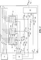
- a radio frequency (RF) circuit 100 includes a power supply 110 configured to generate a plurality of voltages V 1 , V 2 , V 3 - V N (generally designated by reference numeral 115), a plurality of power amplifiers 120A, 120B - 120N (generally designated by reference numeral 120), each having an RF output port 122A, 122B - 122N (generally designated by reference numeral 122) and a power supply input port 124A, 124B - 124N (generally designated by reference numeral 124).
- V 1 , V 2 , V 3 - V N generally designated by reference numeral 115
- a plurality of power amplifiers 120A, 120B - 120N each having an RF output port 122A, 122B - 122N (generally designated by reference numeral 122) and a power supply input port 124A, 124B - 124N (generally designated by reference numeral 124).
- the RF circuit 100 includes a switch network 130 having a plurality of input ports (generally designated by reference numeral 132) coupled to the power supply 110 and a plurality of switch network output ports (generally designated by reference numeral 134) coupled to the power supply input ports 124 of the plurality of power amplifiers 120.
- switch network 130 includes switch circuits 130A, 130B - 130N each of which is coupled to respective power amplifiers 120A, 120B - 120N.
- Each of the switch circuits 130A, 130B - 130N includes a number of switches (generally designated by reference numeral 136) selectively coupled to respective input voltages V 1 , V 2 , V 3 - V N to output selected ones of the voltages 115.
- each of the switch circuits 130A, 130B - 130N includes four switches 136 to select one of the four input voltages V 1 , V 2 , V 3 - V N .
- switch network 130 may be provided including an appropriate number of switch network input ports and switch network output ports.
- the switch network 130 (which in some embodiments may be referred to as a switching circuit) is configured to output selected ones 116A, 116B - 116N (generally designated by reference numeral 116) of the plurality of voltages 115 at the plurality of switch network output ports 134. At least two (i.e., two, three, five, ten, 100, 1000, etc.) of the switch network output port voltages 134 are capable of being different ones of the plurality of voltages 115. As by way of a non-limiting example shown in the RF circuit embodiment of FIG. 1 , three of the selected voltages 116A, 116B, and 116N are different voltages, namely respective input voltages V 1 , V 2 , and V N .
- the selected voltages 116 need not be different.
- a single voltage e.g., V 1
- the switch network 130 is capable of outputting different ones of the input voltages 115, the same input voltage may be selected for output at the switch network output ports 134.
- the RF circuit 100 further includes an RF power combiner circuit 140 having a plurality of input ports 142A, 142B - 142N (generally designated by reference numeral 142) coupled to RF output ports 122 of the plurality of power amplifiers 120, and an output port 144 at which is provided an output signal S out of the RF circuit 100.
- the RF power combiner 140 is an isolating combiner.
- the RF circuit 100 includes a plurality of low-pass filters coupled between the switch network 130 and the power amplifiers 120.
- the low-pass filters can provide pulse shaping to reduce or in some cases minimize and/or even eliminate undesirable high frequency content that may be introduced into a signal primarily caused by rapid changes in the switched supply voltages 115.
- these low-pass filters are nominally low-order LC filters with low loss, but there are many different ways that a low-pass filter can be implemented.
- the parasitic capacitances and inductances always present in any physical circuit, provide enough filtering that an explicit low-pass filter is not required.
- the energy storage of the RF power amplifiers 120 themselves may provide enough filtering that an explicit low-pass filter is not required.
- the RF circuit 100 may be referred to as an asymmetric multilevel outphasing (AMO) architecture for multi-standard transmitters.
- the AMO architecture can be generalized to include two or more power amplifiers, as may be similar to power amplifiers 120 described in conjunction with FIG. 1 . When combined, such two or more power amplifiers are herein referred to as an "M-way" power amplifiers.
- An output of M-way power amplifiers may be described as a vector sum of M different power amplifier outputs, each of which can have two or more different supply voltages, as may be similar to input voltages 115 described in conjunction with FIG. 1 .
- Such two or more supply voltages, when combined, are herein referred to as "N-way" supply voltages.
- each of the M power amplifiers may have an arbitrary phase.
- the RF circuit 100 includes a control system 150 further described herein below.
- the RF circuit 100 is not limited to switch circuits 130A, 130B - 130N for selecting input voltages 115.
- a multiplexor circuit may be used to select the input voltages 115 for output to the power amplifiers 120.
- a further embodiment of a switch network 130' includes one or more switch circuits 130A', each of which is coupled one of the power amplifiers 120 (shown in FIG 1 ).
- FIG. 1B another embodiment of a switch network 130" includes one or more switch circuits 130A", each of which is coupled to one of the power amplifiers 120. It will be understood by one of ordinary skill in the art that some embodiments of a switch network may include combinations of switch circuits (e.g., combinations of switch circuits 130A, 130A', and/or 130A").
- power supply 110 is not limited to any particular type of power supply and includes most any power supply capable of generating the plurality of voltages 115.
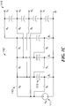
- FIG. 1C a non-limiting example of a switched-capacitor power supply 110' is shown including a voltage supply 111, switches (an example of which is designated by reference numeral 112, and switched capacitors (an example of which is designated by reference numeral 113) to provide voltages 115'. It should be noted that although four voltages are shown, the power supply 110' may generate any number of needed and/or desired voltages.
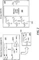
- a schematic circuit diagram of a discrete supply-modulated power amplifier circuit 220 includes a power amplifier 220A coupled through switches 230 to voltage supplies V sup1 , V sup2 - V supN .
- the power amplifier 220A receives an arbitrary phase signal ⁇ in,x .
- the discrete supply-modulated power amplifier circuit 220 may be represented as an equivalent circuit layout 260, which includes a voltage supply 262, resistor 264, and output voltage V x 266.
- a schematic of an M-way AMO power amplifier circuit 270 includes M circuit layouts 260 (an example of which is designated by reference numeral 220') coupled in parallel to a matched, lossy, M-way combiner 280 providing output voltage V out .
- a 4-way matched combiner 380 combines outputs 322 of each of the power amplifiers 320.
- the 4-way matched combiner 380 is realized as a corporate array (or binary tree) of 2-way Wilkinson combiners.
- a combiner may include a binary or "corporate tree" of 2-way combiners, an M-way Wilkinson combiner, and/or a M-way inter-phase transformer with isolation resistors.
- An M-way AMO circuit of the type described herein can be advantageous at high frequencies and power levels. For example, using two or more outphased power amplifiers in an AMO circuit can increase the number of efficiency peaks in power output performance for a given number of supply voltage levels.
- P k is the output power of the k th power amplifier
- V k is the output voltage of the k th power amplifier
- P out is the output power
- V out is the output voltage.
- a graph 400 has a horizontal axis denoting normalized output power in units of decibels (dB) and a vertical axis in percentage of power efficiency.
- a theoretical power efficiency curve 410 is also shown for a conventional linear amplification using non-linear components (LINC) circuit.
- a graph 500 has a horizontal axis denoting normalized output power in arbitrary units of decibels (dB) and a vertical axis in percentage of power efficiency.
- a theoretical power efficiency curve 510 for a conventional LINC circuit. Supply voltages have been selected such that four 100% efficiency points are separated by 3 dB.
- a number of power efficiency peaks increases as M increases.
- An output voltage may be defined as a vector sum of the M voltage vectors from each power amplifier as follows:
- the output voltage vector can be separated into real and imaginary components as follows:
- M unknowns which are the phases of the M power amplifiers.
- M phases There are multiple possible solutions for M phases and, in some cases, no solution exists for a given amplitude A and a given set of voltage levels V k .
- the output amplitude of one power amplifier be A 1 chosen from a discrete set of possible values V k , and that of the other be A 2 , also chosen from the same set of discrete possible values.
- output power and circuit conduction current levels change with the supply voltages delivered to the power amplifiers.
- the circuit conduction losses and switching losses decrease because the power supply input is switched to consecutively lower voltages as power is reduced.
- Gate drive power does not experience similar reductions with output power, which can negatively impact efficiency at low output power levels.
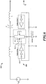
- an AMO power amplifier circuit includes a width-switching device 600 in a switching power amplifier 620, such as a class E switching amplifier.
- a switching power amplifier 620 such as a class E switching amplifier.
- Such a device can parallel the output (drain-source) ports of multiple transistors 611 and drive transistor gates 612 with separately controlled gate drives 614.
- some of the gate drives 614 can be disabled (or otherwise driven to leave transistors 611 off) to save gating power.
- gate drive loss reduction may be traded off for increase in on-state conduction, which can allow optimization of the number of transistor elements gated as a function of power level.
- a number and relative size of width-switching devices 600 can be provided and driven separately at an input source (and operated in parallel at transistor outputs) so as to provide good efficiency over a desired power range.
- width-switching device 600 when V in is relatively large (for example, selected as a large input voltage for high power output), a first gate drive (i.e. gate drive 1) and a second gate drive (i.e., gate drive 2) provide AC gate-drive switching signals to transistors 611.
- a first gate drive i.e. gate drive 1
- a second gate drive i.e., gate drive 2
- V in is relatively large (for example, selected as a large input voltage for high power output)
- one of the gate drive switching signals is modified to hold the gate drive output low to deactivate one of the transistors while another one of transistor is gated on and off.
- first and second gate drives provide substantially similar gating patterns.
- At least one of the gate drives is a plurality of coupled amplifiers.
- width-switching devices could be sized equally in a geometric sizing arrangement (e.g., widths A, 2A, 4A, etc.) or other sizing strategy.
- devices are matched to realize an optimum lowest loss for different power amplifier input voltages of the AMO circuit. This can enable high efficiency at each power supply level in the AMO circuit.
- each of the power amplifiers 120A, 120B - 120N has an RF input port 126A, 126B - 126N (generally designated by reference numeral 126) configured to receive respective phase-adjusted signals ⁇ 1 , ⁇ 2 - ⁇ N (generally denoted by reference numeral 135).
- the switch network 130 is configured to receive a plurality of control signals V C1 , V C2 - V CN (generally designated by reference numerals 125).
- the phase-adjusted signals 135 and control signals 125 control the output signal 144 of the RF circuit.
- a control system 150 which receives as input an amplitude A and a phase ⁇ , is configured to provide the phase-adjusted signals 135 over a plurality of first output ports 154 coupled the RF input ports 126 of the power amplifiers 120 and the control signals 125 over a plurality of second output ports 152 coupled to the switch network 130.
- an AMO circuit 700 includes a control system 750 and an RF circuit 701.
- the control system 750 includes a predistorter 760, an AMO modulator 770, and a digital radio frequency power converter (DRFPC) 780 for modulating a baseband signal comprising amplitude A and phase ⁇ components.
- the RF circuit 701 which may be a further embodiment of the RF circuit embodiment 100 described in conjunction with FIG. 1 , includes a first switch 730A and a second switch 730B for selecting voltage levels 715 supplied to respective first power amplifier 720A and second power amplifier 720B.
- the voltage levels 715 are received from a power supply (not shown) as may be similar to power supply 110 described in conjunction with FIG.
- the AMO modulator 770 drives a fast switching network and switching mode amplifiers, which may include, but are not limited to, class-E, class-F, class- ⁇ , and/or class E/F power amplifiers.
- An RF power combiner 740 combines the outputs of first and second power amplifiers 720A, 720B, while providing isolation between its input ports.
- the predistorter 760 linearizes the combined non-linearity from the DRFPC 780, switches 730A, 730B, and power amplifiers 720A, 720B.
- a polar lookup table 762 is used to store lookup values for amplitude A and phase ⁇ components as will be described herein below.
- the AMO modulator 770 determines a combination of two power voltages 715 supplied to the power amplifiers 720A, 720B based on a peak amplitude within a time interval, which in a further control system embodiment is determined in a interval peak detector.
- the AMO modulator 770 decomposes a predistorted amplitude and phase received from the predistorter 760 into a pair of amplitude values (A 1 , A 2 ) and a pair of phase values ( ⁇ 1 , ⁇ 2 ) using a first-order approximation of equations 3A and 3B described herein below.
- the AMO modulator includes a time aligner 772 to maintain any time delay mismatch between amplitude paths 773 and phase paths 774 to within the margin required by a particular application.
- the DRFPC 780 performs phase modulation by embedding phase components ⁇ 1 , ⁇ 2 of the AMO modulator output into an RF carrier signal.
- the DRFPC 780 includes an array of current steering switches and can bring a significant transmitter power efficiency boost particularly for low output power levels for two reasons. First, the analog matching requirement in the current steering switches is relaxed because the static phase errors in the DRFPC output, which result from analog mismatch, can be corrected by the predistorter 760. Second, the DRFPC 780 does not need baseband active filters for DAC output shaping.
- a graph 790 is a polar representation in coordinates (I, Q) of a baseband signal.
- Half circles (an example of which is designated by reference numeral 792) correspond to discrete amplitude values.
- the graph 790 includes a complex vector 793 at a phase-amplitude baseband constellation point 793A.
- the AMO modulation technique decomposes the complex vector 793 into a first vector 795 and a second vector 797.
- the first and second vectors 795, 797 are a baseband representation of outputs of power amplifiers, as may be similar to power amplifiers 720A and 720B of the RF circuit embodiment 701 described in conjunction with FIG. 7A .
- An outphasing angle ⁇ is defined between the first and second vectors 795, 797.
- C represents a baseband signal over time t
- r i and r j are respective real and imaginary coordinates of baseband signal C.
- A represents amplitude and ⁇ represents the angle.
- ⁇ p is the lookup table value.
- V 1 represents a first voltage level output at time t from the first power amplifier and proportional to the input power supply voltage into the first power amplifier and V 2 represents a second voltage level output at time t from the second power amplifier and proportional to the input power supply voltage into the second power amplifier.
- W represents Wilkinson power combining.
- voltage levels i.e., first voltage level and second voltage level
- the AMO circuit is able to adjust to dynamic power-efficiency needs of an application.
- the AMO modulation technique can be used to optimize efficiency of an RF circuit (as may be similar to RF circuit embodiment 100 described in conjunction with FIG. 1 ) by minimizing power loss in a power combiner (as may be similar to RF power combiner 140 described in conjunction with FIG. 1 ).
- An optimal value of each level r k can be determined, in which levels r k are the maximum output amplitudes A for each supply voltage levels when a power supply drives power amplifiers (as may be similar to power supply 110 and power amplifiers 120A and 120B described in conjunction with FIG. 1 ).
- the total average efficiency can be computed if the amplitude power distribution function (PDF) p(A) of the signal is known. For example, total average efficiency can be computed by dividing the PDF into several regions separated by the r k (and r k combinations), integrating the PDF curve to find the efficiency in each region, and summing the result. For N different supply voltages, there will be N 2 combination of supply voltages given two power amplifiers. However, the power combiner efficiency decreases as the difference between two voltage levels increases. Also, the efficiency improvement may be relatively small when the difference between the two voltages is relatively large. Therefore, the supply voltage combinations can be restricted to adjacent voltage supply levels (i.e., r k and r k+1 ). Using this restriction together with the known PDF of the transmitted signal, the optimum combination of supply voltages can be determined by exhaustive search.
- PDF amplitude power distribution function
- AMO modulation has been described using Wilkinson power combining, one of ordinary skill in the art will readily appreciate that other power combining techniques may be used. Furthermore, although AMO modulation has been described with reference to two power amplifiers, such is not intended as limiting and one of ordinary skill in the art will readily appreciate that more than two power amplifiers may be used.
- an RF circuit 800 includes a plurality of power amplifiers 820, each having an RF output port 822 and an RF power combiner circuit 840 having a plurality of input ports 842 coupled to respective ones of the RF output ports 822 of the plurality of power amplifiers 820.
- the RF power combiner 840 includes a resistance compression network (RCN) 860, a rectification circuit 865 coupled to the resistance compression network 860, and an output port 844 at which is provided an output signal S out of the RF circuit 800.
- the RF circuit output port 844 in some embodiments, is coupled to a load 811, such as an antenna.
- an impedance transformation stage 868 is coupled to an isolation port 848 of the power combiner 840 and the RCN 860.
- the impedance transformation stage 868 matches a RCN impedance to an impedance required by the power combiner 840.
- the RF circuit embodiment 800 of FIG. 8 includes a first power amplifier 820A and a second power amplifier 820B.
- the first power amplifier 820A receives a first signal S 1 (t) output from modulator 821A and the second power amplifier 820B which receives a second signal S 2 (t) output from modulator 821B.
- a source signal S(t) may be fed through a sinusoidal signal source (SCS) to provide signals S 1 (t) and S 2 (t).
- SCS sinusoidal signal source
- a voltage supply 823 provides power to each of the power amplifiers 820A, 820B and recovers power from RF power combiner 840 as will be described herein below.
- the RF-dc converter which recovers the wasted power should provide a constant resistive impedance at its input.
- a purely resistive input impedance can be achieved with a variety of rectifier structures, a non-limiting example of which includes an ideal half bridge rectifier driven by a sinusoidal current source of amplitude I in and frequency ⁇ s , and having a constant output voltage V dc .
- Equation (6) shows that the rectifier input impedance is inversely proportional to input power.
- the equivalent input impedance of the rectifier varies with input power which can reduce the isolation between the power amplifiers and can lower power amplification efficiency (and in some instances, cause complete malfunction) and increase unwanted signal distortion at the output.
- an RCN 860 is included to reduce the rectifier impedance variation.
- the RCN 860 can be combined with an appropriate set of rectifiers 865 to yield an RF-dc converter with narrow-range resistive input characteristics.
- outphasing energy recovery amplifier 800 of FIG. 8 has been described with reference to two power amplifiers 820A, 820B, such is not intended as limiting and one of ordinary skill in the art will readily appreciate that more than two power amplifiers may be used, and that one may choose to use additional resistance compression networks 860 and rectifiers 865 to recover additional energy that would otherwise be dissipated in the power combining process. Moreover, although operation of the outphasing energy recovery amplifier 800 of FIG.
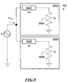
- an RCN 960 includes a first RCN element 960A and a second RCN element 960B, characterized by a resistive input characteristic that varies little as the input power changes.
- the first RCN element 960A includes a first conjugate reactance 962A in series with a first matched load resistance 964A and the second RCN element 960B includes a second conjugate reactance 962B in series with a second matched load resistance 964B.
- First and second RCN elements 960A, 960B represent an equivalent resistance of two rectifiers as given by equation (6).
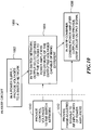
- an RF transmission method 1000 includes, in a power supply, providing voltages to a switch network 1002, in the switch network, outputting selected ones of the voltages to power amplifiers, two or more of the outputted voltages capable of being different 1004, and, in an RF combiner, combining power amplifier outputs and providing an RF circuit output signal 1006.
- the method 1000 includes providing control voltages to the switch network 1010 and providing phase-adjusted signals to RF input ports of the power amplifiers 1012.
- the method 1000 includes decreasing a difference between a sum of the powers outputted by the power amplifiers and an RF power outputted at the output port of the RF circuit. In still a further embodiment, the method 1000 includes minimizing the difference between the sum of the powers outputted by the power amplifiers and the RF power outputted at the output port of the RF circuit.
- the method 1000 includes gating on a variable number of transistors in at least one of the power amplifiers.
- the method 1000 includes, in the RF combiner circuit, providing isolation between the plurality of input ports.
- the method 1000 includes processing at least a portion of the RF power output from the power amplifiers using at least one resistance compression network and at least one rectification circuit coupled to the at least one resistance compression network, wherein the processed RF power includes recovered RF power from the RF power combiner circuit.
Landscapes
- Engineering & Computer Science (AREA)
- Power Engineering (AREA)
- Amplifiers (AREA)
Abstract
Description
- This invention relates to radio frequency (RF) circuits and more particularly to RF amplifier circuits.
- As is known in the art, RF transmitter design is centered on a design tradeoff between the linearity of the power amplifier and its efficiency. This tradeoff relates directly to the usefulness of the resulting device. High linearity results in a higher possible data rate and therefore compatibility with complex standards such as Wireless Local Area Network (WLAN) and Worldwide Interoperability for Microwave Access (WiMAX), and high efficiency allows for reduced cooling, energy usage and power supply requirements (e.g., in stationary applications), and longer use or smaller battery size (e.g., in cell phone and portable applications). The general perception that the tradeoff between linearity and efficiency is fundamental tends to produce designs that compromise between these two design goals. The resulting systems may be either linear or efficient, or are designed specifically for a single communications standard and therefore have limited flexibility of use. Meanwhile, consumer demand for both greater transmission rates and smaller devices continues to drive the need for an architecture that is capable of both linearity and efficiency.
- As is also known in the art, communications standards that support high data rates such as WLAN/WiMAX employ variable-envelope modulation, and so linear amplification is required. One conventional approach is to use an inefficient but highly linear power amplifier. However, there are two main types of transmitter architectures that enable the use of more efficient but non-linear switching mode power amplifiers: (1) polar, and (2) outphasing, or linear amplification of nonlinear components (LINC).
- Conventional polar architectures divide a signal to be amplified into amplitude and phase components. The phase component is used as the input to a non-linear, high-efficiency switching power amplifier, while the amplitude component drives the power supply of the power amplifier to create a varying-envelope signal. While this improves the power amplifier efficiency, it also requires the use of an efficient wide-output range, high-bandwidth power converter. Because converter efficiency degrades dramatically as bandwidth increases, it is very difficult to achieve high efficiency for high data-rate communication standards. This is exacerbated by the 5 - 10X bandwidth expansion that occurs during the conversion from Cartesian to polar coordinates. Thus, this conventional approach is only practical for low-bandwidth systems.
- Outphasing, and specifically conventional LINC architectures, is based on the fact that an arbitrary input signal that can be divided into two constant-amplitude, phase-modulated signals that can each be non-linearly amplified and then passively recombined as a vector sum. This vector sum produces an output signal that is a linearly amplified version of the input. The LINC strategy eliminates the high-bandwidth power converter of the polar architecture, using outphasing to realize amplitude variation. However, the efficiency of the power combining is high only over a small range of output powers. To avoid signal distortion and preserve amplifier efficiency, an isolating combiner is often used. Conventional isolating combiners achieve 100% efficiency only at maximum output power. When the inputs are outphased to vary the amplitude, power is wasted as heat in the isolation resistor. The result is an overall efficiency that is inversely proportional to the peak-to-peak average power ratio (PAPR), limiting the benefits of this conventional approach in high data-rate communication standards such as WiMAX, in which the PAPR is high.
- One of the major drawbacks of the LINC architecture is the power wasted in the power combiner. However, a combiner must be used to isolate outphased power amplifiers and provide a fixed impedance load to the power amplifiers in order to avoid signal distortion and preserve switching amplifier efficiency. But power is wasted as heat in the combiner resistor when the inputs are outphased to vary the amplitude. Since the power delivered to the combiner by power amplifiers is constant, the efficiency of the LINC system is directly proportional to the output power sent to a load. The time-averaged efficiency is therefore inversely proportional to the peak-to-average power ratio (PAPR). Unfortunately, high-level modulation schemes such as 64-QAM and OFDM tend to have high PAPR, leading to low average efficiency when the LINC system is used.
- To alleviate the problem of wasted energy during outphasing, sometimes non-isolating combiners are used. The Chireix combiner is a prominent example which uses compensating reactive elements to enhance the power-combining efficiency. However, the Chireix combiner can only be tuned for a very small range of outphase angles. With outphase angles outside the tuned range, the load impedance presented to the power amplifiers deviates too far from the nominal value and the isolation between the power amplifier outputs becomes poor. The result is significant distortion and degraded amplification efficiency.
- One proposed power recycling technique described in Zhang X., et al. "Analysis of power recycling techniques for RF and microwave outphasing power amplifiers," IEEE Trans. Circuit Syst. II, vol. 49, no. 5, May 2002, pp. 312 - 320, attempts to enhance the power efficiency of the LINC architecture without giving up the simplicity of an isolating combiner. The isolation resistor is replaced with an RF-dc converter to recover the wasted power back to the power supply. While this approach has been shown to result in a significant increase in the overall efficiency, it suffers from excessive impedance variation at the isolation port and therefore incomplete isolation between power amplifiers. This can lead to excessive signal distortion and lower efficiency or even complete breakdown in the power amplifiers, particularly in those sensitive to load impedance, such as many switched-mode power amplifiers. An additional isolator can be added between the isolation port and the RF-dc converter to reduce this effect, but at the cost of added complexity and loss.
- In general overview, the circuits, concepts, and techniques described herein provide an asymmetric multilevel outphasing (AMO) transmitter architecture which includes a switch network capable of supplying discrete voltages to power amplifiers. The power amplifiers are power combined to provide an output signal over a wide power range. An AMO modulation technique is used to minimize amplifier outphasing angles to achieve higher efficiency and linearity in a transmission architecture. The result is a highly efficiency architecture that is compatible with a wide range of communication standards and applications. For example, the inventive concepts, circuits, and techniques described herein may be used to provide highly efficient military and/or commercial transmitters for use in handheld units, laptop wireless modems, and base stations. The inventive concepts, circuits and techniques may also be used to provide high-efficiency RF power amplification for medical applications (such as RF amplifiers for Magnetic Resonance Imaging) and industrial and commercial applications (such as plasma generation, heating, coating, and sintering),
- In one aspect, a radio frequency (RF) circuit includes a power supply configured to generate a plurality of voltages, a plurality of power amplifiers, each having an RF output port and a power supply input port, a switch network having a plurality of input ports coupled to the power supply and a plurality of switch network output ports coupled to the power supply input ports of the plurality of power amplifiers, wherein the switch network is configured to output selected ones of the plurality of voltages from the plurality of switch network output ports, at least two of the switch network output port voltages capable of being different ones of the plurality of voltages, and an RF power combiner circuit having a plurality of input ports coupled to RF output ports of the plurality of power amplifiers and an output port at which is provided an output signal of the RF circuit.
- In further embodiments, the RF circuit includes one or more of the following features: each of the power amplifiers has an RF input port configured to receive a phase-adjusted signal and the switch network is configured to receive a plurality of control signals, wherein the phase-adjusted signals and the switch network control signals are used to control the output signal of the RF circuit; a control system configured to provide the phase-adjusted signals over a plurality of first output ports coupled to the RF input ports of the plurality of power amplifiers and the plurality of control signals over a plurality of second output ports coupled to the switch network; the control system is further configured to decrease a difference between a total of the power output from the plurality of power amplifiers and a power output from the RF circuit; the RF power combiner circuit includes an isolating combiner; the power combiner circuit further includes a resistance compression network and a rectification circuit coupled to the resistance compression network; a plurality of LC filters configured to couple the switch network to respective ones of the plurality of power amplifiers, and; at least one of the power amplifiers is width-switched.
- In another aspect, the concepts, circuits, and techniques described herein are directed to an outphasing energy recovery amplifier (OPERA) architecture that substantially reduces the impedance variation at an isolation port of a combiner through the use of a resistance compression network (RCN). The RCN improves the matching and isolation between outphased amplifiers, helping to maintain high linearity as well as high efficiency in switching-mode amplifiers.
- The OPERA architecture includes circuitry to recover power that would otherwise be wasted in an isolation resistor back to a power supply. In some embodiments, the isolation resistor is replaced with an RF-dc converter. The equivalent input impedance of the rectifier varies with input power which can reduce the isolation between the power amplifiers and can lower power amplification efficiency (and in some instances, cause complete malfunction) and increase unwanted signal distortion at the output. To mitigate these unwanted effects, a RCN is included to reduce the rectifier impedance variation. In some embodiments, an impedance transformation stage is placed between the RCN and the power combiner's isolation port to match the resistance-compressed rectifier impedance to the impedance required by the power combiner.
- In another aspect, a radio frequency (RF) circuit includes a plurality of power amplifiers, each having an RF output port, and an RF power combiner circuit having a plurality of input ports coupled to respective ones of the RF output ports of the plurality of power amplifiers, and including a resistance compression network, a rectification circuit coupled to the resistance compression network, and an output port at which is provided an output signal of the RF circuit.
- In further embodiments, the RF circuit includes one or more of the following features: the RF power combiner circuit provides isolation between the plurality of RF power combiner circuit input ports; each of the power amplifiers has a power supply input port and further including a power supply providing voltages at a plurality of power supply output ports, wherein at least two of the power supply output ports provide different voltages, and a switching circuit to selectively couple each power amplifier power supply input port to at least one of the power supply output ports, and; each of the power amplifiers has an RF input port configured to receive a phase adjusted signal and the switching circuit is configured to receive at least one control signal, wherein the phase adjusted signals and the at least one switching circuit control signal are used to control the output signal of the RF circuit.
- In a further aspect, a radio frequency (RF) transmission method includes providing a plurality of voltages, outputting selected ones of the plurality of voltages to a plurality of power amplifiers, at least two of the outputted voltages capable of being different ones of the plurality of voltages, and providing an RF power combiner circuit having a plurality of input ports coupled to the plurality of power amplifiers, and an output port at which is provided an output signal of the RF circuit.
- In further embodiments, the method includes one or more of the following features: providing a power supply to generate the plurality of voltages, providing the plurality of voltages to a plurality of input ports of a switch network, and in the switch network, providing the selected ones of the plurality of voltages to RF input ports of the plurality of power amplifiers; each of the power amplifiers has an RF input port, further including controlling the output signal of the RF circuit by adjusting the phases of the signals received at the RF input ports and dynamically selecting the ones of the plurality of voltages outputted to each of the power amplifiers; decreasing a difference between a sum of the powers outputted by the power amplifiers and an RF power outputted at the output port of the RF circuit; said decreasing includes minimizing the difference between the sum of the powers outputted by the power amplifiers and the RF power outputted at the output port of the RF circuit; gating on a variable number of transistors in at least one of the power amplifiers; providing isolation between the plurality of input ports, and; processing at least a portion of the RF power output from the power amplifiers using at least one resistance compression network and at least one rectification circuit coupled to the at least one resistance compression network, wherein the processed RF power includes recovered RF power from the RF power combiner circuit.
- The foregoing features of concepts, circuits, and techniques described herein may be more fully understood from the following description of the drawings in which:
-
FIG. 1 is a block diagram of an embodiment of an asymmetric multilevel outphasing (AMO) circuit; -
FIG. 1A is a circuit diagram of an embodiment of a switch network as may be used in the AMO circuit ofFIG. 1 ; -
FIG. 1B is a circuit diagram of another embodiment of a switch network as may be used in the AMO circuit ofFIG. 1 ; -
FIG. 1C is an exemplary embodiment of a power supply as may be used for supplying voltages to the AMO circuit ofFIG. 1 ; -
FIG. 2 is a schematic circuit diagram of an M-way power amplifier/N-way voltage level AMO circuit embodiment; -
FIG. 3 is a block diagram of 4-way power amplifier/4-way voltage level AMO circuit embodiment including a 4-way matched combiner; -
FIG. 4 is a graph showing power efficiency curves of AMO circuit embodiments having 2-way voltage levels; -
FIG. 5 is another graph showing power efficiency curves of further AMO circuit embodiments having 4-way voltage levels; -
FIG. 6 is a circuit diagram of a width-switched power amplifier embodiment; -
FIG. 7A is a block diagram of a two power amplifier/four voltage level circuit embodiment including a control system; -
FIG. 7B is polar coordinate graphical representation of coordinates (I, Q) of a baseband signal; -
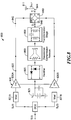
FIG. 8 is a block diagram of an embodiment of an outphasing energy recovery amplifier; -
FIG. 9 is a block diagram of an embodiment of a resistance compression network embodiment used in the amplifier embodiment ofFIG. 8 ; and -
FIG. 10 is a flow diagram of an asymmetric multilevel outphasing transmission method. - Referring now to
FIG. 1 , in one aspect a radio frequency (RF)circuit 100 includes apower supply 110 configured to generate a plurality of voltages V1, V2, V3 - VN (generally designated by reference numeral 115), a plurality ofpower amplifiers RF output port supply input port RF circuit 100 includes aswitch network 130 having a plurality of input ports (generally designated by reference numeral 132) coupled to thepower supply 110 and a plurality of switch network output ports (generally designated by reference numeral 134) coupled to the powersupply input ports 124 of the plurality ofpower amplifiers 120. - In the RF circuit embodiment of
FIG. 1 ,switch network 130 includesswitch circuits respective power amplifiers switch circuits voltages 115. For example, each of theswitch circuits switches 136 to select one of the four input voltages V1, V2, V3 - VN. It should be noted that although four input voltages (and four respective switches) are shown, one of ordinary skill in the art will readily appreciate that any number of input voltages may be used, for example, two, three, five, ten, 100, 1000, etc., andswitch network 130 may be provided including an appropriate number of switch network input ports and switch network output ports. - The switch network 130 (which in some embodiments may be referred to as a switching circuit) is configured to output selected
ones voltages 115 at the plurality of switchnetwork output ports 134. At least two (i.e., two, three, five, ten, 100, 1000, etc.) of the switch networkoutput port voltages 134 are capable of being different ones of the plurality ofvoltages 115. As by way of a non-limiting example shown in the RF circuit embodiment ofFIG. 1 , three of the selectedvoltages - It should be noted that the selected
voltages 116 need not be different. For example, a single voltage (e.g., V1) may be selected for output at the switchnetwork output ports 134. In other words, even though theswitch network 130 is capable of outputting different ones of the input voltages 115, the same input voltage may be selected for output at the switchnetwork output ports 134. - The
RF circuit 100 further includes an RFpower combiner circuit 140 having a plurality ofinput ports RF output ports 122 of the plurality ofpower amplifiers 120, and anoutput port 144 at which is provided an output signal Sout of theRF circuit 100. In a further embodiment, theRF power combiner 140 is an isolating combiner. - In another embodiment, the
RF circuit 100 includes a plurality of low-pass filters coupled between theswitch network 130 and thepower amplifiers 120. The low-pass filters can provide pulse shaping to reduce or in some cases minimize and/or even eliminate undesirable high frequency content that may be introduced into a signal primarily caused by rapid changes in the switchedsupply voltages 115. In some embodiments, these low-pass filters are nominally low-order LC filters with low loss, but there are many different ways that a low-pass filter can be implemented. For example, another possibility is that the parasitic capacitances and inductances, always present in any physical circuit, provide enough filtering that an explicit low-pass filter is not required. A further possibility is that the energy storage of theRF power amplifiers 120 themselves (such as owing to the use of RF input chokes or inductors) may provide enough filtering that an explicit low-pass filter is not required. - In one or more embodiments, the
RF circuit 100 may be referred to as an asymmetric multilevel outphasing (AMO) architecture for multi-standard transmitters. The AMO architecture can be generalized to include two or more power amplifiers, as may be similar topower amplifiers 120 described in conjunction withFIG. 1 . When combined, such two or more power amplifiers are herein referred to as an "M-way" power amplifiers. An output of M-way power amplifiers may be described as a vector sum of M different power amplifier outputs, each of which can have two or more different supply voltages, as may be similar toinput voltages 115 described in conjunction withFIG. 1 . Such two or more supply voltages, when combined, are herein referred to as "N-way" supply voltages. Furthermore, each of the M power amplifiers may have an arbitrary phase. - In further embodiments, the
RF circuit 100 includes acontrol system 150 further described herein below. - It will be appreciated by one of ordinary skill in the art that the
RF circuit 100 is not limited to switchcircuits input voltages 115. As by way of non-limiting examples, a multiplexor circuit may be used to select theinput voltages 115 for output to thepower amplifiers 120. - Referring now to
FIG. 1A , a further embodiment of a switch network 130' includes one ormore switch circuits 130A', each of which is coupled one of the power amplifiers 120 (shown inFIG 1 ). - Referring now to
FIG. 1B , another embodiment of aswitch network 130" includes one ormore switch circuits 130A", each of which is coupled to one of thepower amplifiers 120. It will be understood by one of ordinary skill in the art that some embodiments of a switch network may include combinations of switch circuits (e.g., combinations ofswitch circuits - Referring again to
FIG. 1 , it should be noted thatpower supply 110 is not limited to any particular type of power supply and includes most any power supply capable of generating the plurality ofvoltages 115. Referring now toFIG. 1C , a non-limiting example of a switched-capacitor power supply 110' is shown including avoltage supply 111, switches (an example of which is designated byreference numeral 112, and switched capacitors (an example of which is designated by reference numeral 113) to provide voltages 115'. It should be noted that although four voltages are shown, the power supply 110' may generate any number of needed and/or desired voltages. - Referring now to
FIG. 2 , a schematic circuit diagram of a discrete supply-modulatedpower amplifier circuit 220 includes apower amplifier 220A coupled throughswitches 230 to voltage supplies Vsup1, Vsup2 - VsupN. Thepower amplifier 220A receives an arbitrary phase signal Φin,x. - The discrete supply-modulated
power amplifier circuit 220 may be represented as anequivalent circuit layout 260, which includes avoltage supply 262,resistor 264, andoutput voltage V x 266. A schematic of an M-way AMOpower amplifier circuit 270 includes M circuit layouts 260 (an example of which is designated by reference numeral 220') coupled in parallel to a matched, lossy, M-way combiner 280 providing output voltage Vout. - Referring now to
FIG. 3 , an example of an M-way, N-way circuit 300 is shown in which M = 4 and N = 4. A 4-way matchedcombiner 380combines outputs 322 of each of thepower amplifiers 320. The 4-way matchedcombiner 380 is realized as a corporate array (or binary tree) of 2-way Wilkinson combiners. - It will be appreciated by one of ordinary skill in the art that other types of combiners may be used. As by way of non-limiting examples, a combiner may include a binary or "corporate tree" of 2-way combiners, an M-way Wilkinson combiner, and/or a M-way inter-phase transformer with isolation resistors.
- An M-way AMO circuit of the type described herein can be advantageous at high frequencies and power levels. For example, using two or more outphased power amplifiers in an AMO circuit can increase the number of efficiency peaks in power output performance for a given number of supply voltage levels. The efficiency for a given supply voltage combination using a matched isolating M-way combiner can be calculated as follows:

- Here, Pk is the output power of the kth power amplifier, Vk is the output voltage of the kth power amplifier, Pout is the output power, and Vout is the output voltage. This assumes 100% efficient power amplifiers and no combiner insertion loss. Note that if a symmetric dissipative isolating combiner is used, 100% efficiency can only be obtained when all the voltages being combined have the same amplitude. Therefore, there will be exactly N points of 100% efficiency in power output performance. When the voltages being combined have different amplitudes, there is loss in the combiner's isolation resistors.
- Referring now to
FIG. 4 , agraph 400 has a horizontal axis denoting normalized output power in units of decibels (dB) and a vertical axis in percentage of power efficiency. Ingraph 400, theoretical power efficiency curves 402, 404, 406 are shown for respective M-way AMO circuits in which M=2, 3, 4, respectively, and in which N=2 voltage supply levels. A theoreticalpower efficiency curve 410 is also shown for a conventional linear amplification using non-linear components (LINC) circuit. The power efficiency curve for a given value of M (i.e., M=2, M=3, etc.) may be generated by first computing the efficiency vs. output power for each possible voltage combination, setting the efficiency to 0 if a given output power is unachievable for a given voltage combination, and taking the maximum efficiency over the different possible voltage combinations. Supply voltages have been selected such that two 100% efficiency points are separated by 6 dB. As can be readily seen inFIG. 4 , a number of power efficiency peaks (an example of which is denoted by reference numeral 411) increases as M increases. - Referring now to
FIG. 5 , agraph 500 has a horizontal axis denoting normalized output power in arbitrary units of decibels (dB) and a vertical axis in percentage of power efficiency. Ingraph 500, theoretical efficiency curves 502, 504, 506 are shown for respective M-way AMO circuits in which M=2, 3, 4 and in which N=4 voltage supply levels. Also shown is a theoreticalpower efficiency curve 510 for a conventional LINC circuit. Supply voltages have been selected such that four 100% efficiency points are separated by 3 dB. As can be readily seen inFIG. 5 , a number of power efficiency peaks (an example of which is denoted by reference numeral 511) increases as M increases. - For a given output voltage vector Vout = A·exp(j·θ) and a given combination of power amplifier supply voltages, the phases for each of the power amplifiers can be computed as described herein below.
- An output voltage may be defined as a vector sum of the M voltage vectors from each power amplifier as follows:

- The output voltage vector can be separated into real and imaginary components as follows:


- These two equations yield M unknowns, which are the phases of the M power amplifiers. There are multiple possible solutions for M phases and, in some cases, no solution exists for a given amplitude A and a given set of voltage levels Vk. For purposes of illustration, the outphasing angles and voltage supply levels are calculated in such way as to minimize energy loss. Described here is method for the case of M = 2. However, it should be understood that the method can be generalized to handle cases for which M > 2.
- In order to achieve an output vector with amplitude A, let the output amplitude of one power amplifier be A1 chosen from a discrete set of possible values Vk, and that of the other be A2, also chosen from the same set of discrete possible values. For each possible value of A1 and A2, the efficiency of the power combining operation can be calculated using the formula:

- All combinations of A1 and A2 for which this formula evaluates to a value exceeding 1 are impossible choices for realizing the output amplitude A. The values of A1 and A2 for which ηc is maximized (without exceeding 1) are the most efficient choices. That is, they result in the minimum outphasing angle and the minimum amount of wasted energy. Once the values A1 and A2 are chosen, the proper phases for the two power amplifiers are given by the following equations:


- In an AMO power amplifier circuit, as may be similar to
RF circuit embodiment 100 described in conjunction withFIG. 1 , output power and circuit conduction current levels change with the supply voltages delivered to the power amplifiers. The circuit conduction losses and switching losses decrease because the power supply input is switched to consecutively lower voltages as power is reduced. Gate drive power, however, does not experience similar reductions with output power, which can negatively impact efficiency at low output power levels. - Referring now to
FIG. 6 , in some embodiments, an AMO power amplifier circuit includes a width-switchingdevice 600 in aswitching power amplifier 620, such as a class E switching amplifier. Such a device can parallel the output (drain-source) ports ofmultiple transistors 611 and drivetransistor gates 612 with separately controlled gate drives 614. At low power levels, some of the gate drives 614 can be disabled (or otherwise driven to leavetransistors 611 off) to save gating power. In such a way, gate drive loss reduction may be traded off for increase in on-state conduction, which can allow optimization of the number of transistor elements gated as a function of power level. More particularly, a number and relative size of width-switchingdevices 600 can be provided and driven separately at an input source (and operated in parallel at transistor outputs) so as to provide good efficiency over a desired power range. - In an exemplary operation of width-switching
device 600, when Vin is relatively large (for example, selected as a large input voltage for high power output), a first gate drive (i.e. gate drive 1) and a second gate drive (i.e., gate drive 2) provide AC gate-drive switching signals totransistors 611. Alternatively, when Vin is relatively small (for example, selected as a small input voltage for lower power output) one of the gate drive switching signals is modified to hold the gate drive output low to deactivate one of the transistors while another one of transistor is gated on and off. - In a further embodiment, first and second gate drives provide substantially similar gating patterns.
- In another embodiment, at least one of the gate drives is a plurality of coupled amplifiers.
- In a further embodiment, more than two width-switching devices could be sized equally in a geometric sizing arrangement (e.g., widths A, 2A, 4A, etc.) or other sizing strategy. In still further embodiments, devices are matched to realize an optimum lowest loss for different power amplifier input voltages of the AMO circuit. This can enable high efficiency at each power supply level in the AMO circuit.
- Referring again to
FIG. 1 , in a further RF circuit embodiment each of thepower amplifiers RF input port switch network 130 is configured to receive a plurality of control signals VC1, VC2 - VCN (generally designated by reference numerals 125). As will be described herein below, the phase-adjustedsignals 135 andcontrol signals 125 control theoutput signal 144 of the RF circuit. - In still a further embodiment, a
control system 150, which receives as input an amplitude A and a phase Φ, is configured to provide the phase-adjustedsignals 135 over a plurality offirst output ports 154 coupled theRF input ports 126 of thepower amplifiers 120 and the control signals 125 over a plurality ofsecond output ports 152 coupled to theswitch network 130. - Referring now to
FIG. 7A , in a further embodiment anAMO circuit 700 includes acontrol system 750 and anRF circuit 701. Thecontrol system 750 includes apredistorter 760, anAMO modulator 770, and a digital radio frequency power converter (DRFPC) 780 for modulating a baseband signal comprising amplitude A and phase Φ components. TheRF circuit 701, which may be a further embodiment of theRF circuit embodiment 100 described in conjunction withFIG. 1 , includes afirst switch 730A and asecond switch 730B for selectingvoltage levels 715 supplied to respectivefirst power amplifier 720A andsecond power amplifier 720B. Thevoltage levels 715 are received from a power supply (not shown) as may be similar topower supply 110 described in conjunction withFIG. 1 . In a further embodiment, theAMO modulator 770 drives a fast switching network and switching mode amplifiers, which may include, but are not limited to, class-E, class-F, class-Φ, and/or class E/F power amplifiers. AnRF power combiner 740 combines the outputs of first andsecond power amplifiers - The
predistorter 760 linearizes the combined non-linearity from theDRFPC 780, switches 730A, 730B, andpower amplifiers power voltages 715 supplied to thepower amplifiers predistorter 760 into a pair of amplitude values (A1, A2) and a pair of phase values (Φ1, Φ2) using a first-order approximation of equations 3A and 3B described herein below. In a further embodiment, the AMO modulator includes atime aligner 772 to maintain any time delay mismatch betweenamplitude paths 773 andphase paths 774 to within the margin required by a particular application. - The
DRFPC 780 performs phase modulation by embedding phase components Φ1, Φ2 of the AMO modulator output into an RF carrier signal. TheDRFPC 780 includes an array of current steering switches and can bring a significant transmitter power efficiency boost particularly for low output power levels for two reasons. First, the analog matching requirement in the current steering switches is relaxed because the static phase errors in the DRFPC output, which result from analog mismatch, can be corrected by thepredistorter 760. Second, theDRFPC 780 does not need baseband active filters for DAC output shaping. - Referring now to
FIG. 7B , an exemplary operation of an asymmetric multilevel outphasing (AMO) modulation technique to determine control voltages and phase components will now be described. Agraph 790 is a polar representation in coordinates (I, Q) of a baseband signal. Half circles (an example of which is designated by reference numeral 792) correspond to discrete amplitude values. Thegraph 790 includes acomplex vector 793 at a phase-amplitudebaseband constellation point 793A. - The AMO modulation technique decomposes the
complex vector 793 into afirst vector 795 and asecond vector 797. The first andsecond vectors power amplifiers RF circuit embodiment 701 described in conjunction withFIG. 7A . An outphasing angle θ is defined between the first andsecond vectors - Mathematically, AMO modulation technique can be defined with the polar representation of the baseband signal, according to the following equation:

- Here, C represents a baseband signal over time t, and ri and rj are respective real and imaginary coordinates of baseband signal C. In equation (1), A represents amplitude and θ represents the angle.
- C(t) can be linearized by predistorting power amplifier output using a polar lookup table (as may be similar to polar lookup table 762 described in conjunction with
FIG. 7A ) using the following equation:
- Here, θp is the lookup table value. In an RF circuit including a first and a second power amplifier (as may be similar to
RF circuit 701 described in conjunction withFIG. 7A ), P(t) can be decomposed into two parts using the following equation:
- Here, V1 represents a first voltage level output at time t from the first power amplifier and proportional to the input power supply voltage into the first power amplifier and V2 represents a second voltage level output at time t from the second power amplifier and proportional to the input power supply voltage into the second power amplifier. W represents Wilkinson power combining. In this way, voltage levels (i.e., first voltage level and second voltage level) can be dynamically selected over time and/or at various times during operation of the AMO circuit. Advantageously, the AMO circuit is able to adjust to dynamic power-efficiency needs of an application.
- A first phase component Φ1 representing a first phase input to the first power amplifier and a second phase component Φ2 representing a second phase input to a second power amplifier can be calculated as follows:


- The AMO modulation technique can be used to optimize efficiency of an RF circuit (as may be similar to
RF circuit embodiment 100 described in conjunction withFIG. 1 ) by minimizing power loss in a power combiner (as may be similar toRF power combiner 140 described in conjunction withFIG. 1 ). An optimal value of each level rk can be determined, in which levels rk are the maximum output amplitudes A for each supply voltage levels when a power supply drives power amplifiers (as may be similar topower supply 110 andpower amplifiers FIG. 1 ). The Wilkinson combiner efficiency at a given output amplitude A driven by two power amplifiers with different supply voltages can be represented according to the following equation:
- Equation (4) simplifies to a standard Wilkinson efficiency when rk = rj. The total average efficiency can be computed if the amplitude power distribution function (PDF) p(A) of the signal is known. For example, total average efficiency can be computed by dividing the PDF into several regions separated by the rk (and rk combinations), integrating the PDF curve to find the efficiency in each region, and summing the result. For N different supply voltages, there will be

- Although AMO modulation has been described using Wilkinson power combining, one of ordinary skill in the art will readily appreciate that other power combining techniques may be used. Furthermore, although AMO modulation has been described with reference to two power amplifiers, such is not intended as limiting and one of ordinary skill in the art will readily appreciate that more than two power amplifiers may be used.
- Referring now to
FIG. 8 , in another aspect anRF circuit 800 includes a plurality ofpower amplifiers 820, each having anRF output port 822 and an RFpower combiner circuit 840 having a plurality ofinput ports 842 coupled to respective ones of theRF output ports 822 of the plurality ofpower amplifiers 820. TheRF power combiner 840 includes a resistance compression network (RCN) 860, arectification circuit 865 coupled to theresistance compression network 860, and anoutput port 844 at which is provided an output signal Sout of theRF circuit 800. The RFcircuit output port 844, in some embodiments, is coupled to aload 811, such as an antenna. - In a further embodiment, an
impedance transformation stage 868 is coupled to anisolation port 848 of thepower combiner 840 and theRCN 860. Theimpedance transformation stage 868 matches a RCN impedance to an impedance required by thepower combiner 840. - The
RF circuit embodiment 800 ofFIG. 8 includes afirst power amplifier 820A and asecond power amplifier 820B. In some embodiments, thefirst power amplifier 820A receives a first signal S1(t) output frommodulator 821A and thesecond power amplifier 820B which receives a second signal S2(t) output frommodulator 821B. In the same or different embodiment, a source signal S(t) may be fed through a sinusoidal signal source (SCS) to provide signals S1(t) and S2(t). Avoltage supply 823 provides power to each of thepower amplifiers RF power combiner 840 as will be described herein below. - An exemplary operation of the
RF circuit embodiment 800 will now be described. Because thepower combiner 840 requires a fixed resistance at theisolation port 848 to ensure matching and isolation between the first and secondoutphased power amplifiers - Driving a rectifier (such as the above-described ideal half bridge rectifier) with a tuned network suppresses the harmonic content inherent in rectifier operation and results in a resistive impedance characteristic at a desired frequency. This equivalent resistance can be represented by the following equation:
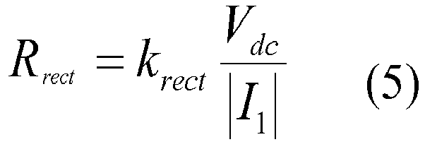
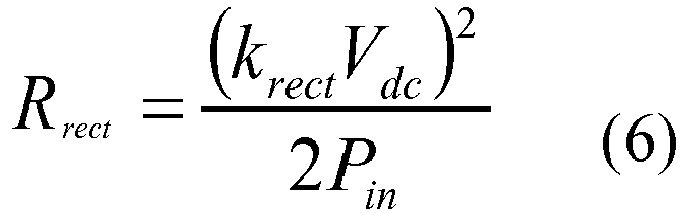
- Equation (6) shows that the rectifier input impedance is inversely proportional to input power. The equivalent input impedance of the rectifier varies with input power which can reduce the isolation between the power amplifiers and can lower power amplification efficiency (and in some instances, cause complete malfunction) and increase unwanted signal distortion at the output.
- To mitigate these unwanted effects, an
RCN 860 is included to reduce the rectifier impedance variation. TheRCN 860 can be combined with an appropriate set ofrectifiers 865 to yield an RF-dc converter with narrow-range resistive input characteristics. - Although operation of the outphasing
energy recovery amplifier 800 ofFIG. 8 has been described with reference to twopower amplifiers resistance compression networks 860 andrectifiers 865 to recover additional energy that would otherwise be dissipated in the power combining process. Moreover, although operation of the outphasingenergy recovery amplifier 800 ofFIG. 8 has been shown with energy recovery directly to a power supply applied to the twoamplfiers power amplifiers 820 could be derived elsewhere (e.g., for AMO modulation). - Referring now to
FIG. 9 , in some embodiments anRCN 960 includes afirst RCN element 960A and asecond RCN element 960B, characterized by a resistive input characteristic that varies little as the input power changes. Thefirst RCN element 960A includes a firstconjugate reactance 962A in series with a first matchedload resistance 964A and thesecond RCN element 960B includes a secondconjugate reactance 962B in series with a second matchedload resistance 964B. First andsecond RCN elements RCN 960 will be resistive with a value RRCN indicated as follows:
- In this way, compression of matched load resistances Rrect is provided about a center value of impedance X. For variations of Rrect over a range having a geometric mean of X (i.e., Rrectε [(X/Crect 1/2), Crect 1/2X], where crect is the ratio of the largest to smallest resistances in the Rrect range), the corresponding ratio of the compressed RRCN range can be shown to be as follows:
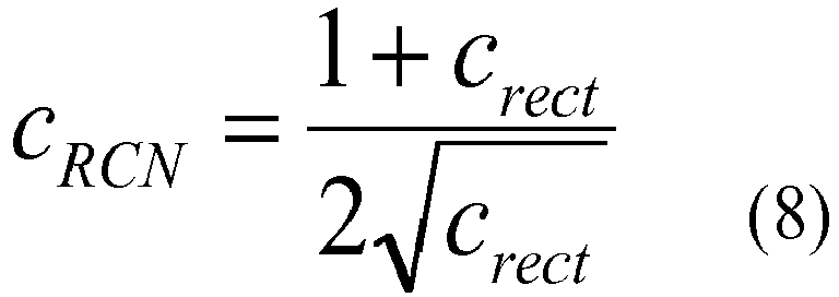
- For example, a 10:1 variation in Rrect (Crect = 10) results in a modest 1.74:1 variation in RRCN. Since Rrect is inversely proportional to Pin as shown in equation (6), this means a 10:1 variation in power delivered to the isolation port would result in only a 1.74:1 variation in isolation port resistance. This narrowed range of resistance will result in substantially improved isolation between the outphased power amplifiers (as may be similar to
outphased power amplifiers FIG. 8 ), greatly improving amplification efficiency. - It should be noted that at sufficiently high output power levels (i.e., low power levels to the rectifiers), the rectifier resistance can no longer be effectively compressed. This is because at low input power levels, the diodes will be unable to turn "on" and overcome the combination of supply voltage and diode built-in potential. When the diodes turn "off", equations (5) and (6) are no longer valid and the efficiency of the RCN drops considerably. However, this poses no serious problems. In this region of operation, most of the power from the power amplifiers is delivered to the load, and so the isolation port acts as a virtual open circuit. Therefore, the rectifier impedance and the efficiency of the RCN do not matter.
- Referring now to
FIG. 10 , anRF transmission method 1000 includes, in a power supply, providing voltages to aswitch network 1002, in the switch network, outputting selected ones of the voltages to power amplifiers, two or more of the outputted voltages capable of being different 1004, and, in an RF combiner, combining power amplifier outputs and providing an RFcircuit output signal 1006. In a further embodiment, themethod 1000 includes providing control voltages to theswitch network 1010 and providing phase-adjusted signals to RF input ports of thepower amplifiers 1012. - In a further embodiment, the
method 1000 includes decreasing a difference between a sum of the powers outputted by the power amplifiers and an RF power outputted at the output port of the RF circuit. In still a further embodiment, themethod 1000 includes minimizing the difference between the sum of the powers outputted by the power amplifiers and the RF power outputted at the output port of the RF circuit. - In a further embodiment, the
method 1000 includes gating on a variable number of transistors in at least one of the power amplifiers. - In a further embodiment, the
method 1000 includes, in the RF combiner circuit, providing isolation between the plurality of input ports. - In a further embodiment, the
method 1000 includes processing at least a portion of the RF power output from the power amplifiers using at least one resistance compression network and at least one rectification circuit coupled to the at least one resistance compression network, wherein the processed RF power includes recovered RF power from the RF power combiner circuit. - Having described embodiments of the concepts, circuits, and techniques described herein, it will now become apparent to one of ordinary skill in the art that other embodiments incorporating these concepts, circuits, and techniques may be used. It is felt therefore that these embodiments should not be limited to disclosed embodiments, but rather should be limited only by the spirit and scope of the appended claims.
- Embodiments of the invention can be described with reference to the following numbered clauses, with preferred features laid out in the dependent clauses:
-
Clause 1. A radio frequency (RF) circuit comprising: a power supply configured to generate a plurality of voltages; a plurality of power amplifiers, each having an RF output port and a power supply input port; a switch network having a plurality of input ports coupled to the power supply and a plurality of switch network output ports coupled to the power supply input ports of the plurality of power amplifiers, wherein the switch network is configured to output selected ones of the plurality of voltages from the plurality of switch network output ports, at least two of the switch network output port voltages capable of being different ones of the plurality of voltages; and an RF power combiner circuit having a plurality of input ports coupled to RF output ports of the plurality of power amplifiers and an output port at which is provided an output signal of the RF circuit. -
Clause 2. The RF circuit ofclaim 1 , wherein each of the power amplifiers has an RF input port configured to receive a phase-adjusted signal and the switch network is configured to receive a plurality of control signals, wherein the phase-adjusted signals and the switch network control signals are used to control the output signal of the RF circuit. - Clause 3. The RF circuit of
claim 2, further comprising: a control system configured to provide the phase-adjusted signals over a plurality of first output ports coupled to the RF input ports of the plurality of power amplifiers and the plurality of control signals over a plurality of second output ports coupled to the switch network. -
Clause 4. The RF circuit of claim 3, wherein the control system is further configured to decrease a difference between a total of the power output from the plurality of power amplifiers and a power output from the RF circuit. -
Clause 5. The RF circuit ofclaim 1 , wherein the RF power combiner circuit includes an isolating combiner. -
Clause 6. The RF circuit ofclaim 1 , wherein the power combiner circuit further comprises: a resistance compression network; and a rectification circuit coupled to the resistance compression network. - Clause 7. The RF circuit of
claim 1 , further comprising a plurality of LC filters configured to couple the switch network to respective ones of the plurality of power amplifiers. -
Clause 8. The RF circuit ofclaim 1 , wherein at least one of the power amplifiers is width- switched. - Clause 9. A radio frequency (RF) circuit comprising: a plurality of power amplifiers, each having an RF output port; and an RF power combiner circuit having a plurality of input ports coupled to respective ones of the RF output ports of the plurality of power amplifiers, comprising: a resistance compression network; a rectification circuit coupled to the resistance compression network; and an output port at which is provided an output signal of the RF circuit.
-
Clause 10. The RF circuit of claim 9, wherein the RF power combiner circuit provides isolation between the plurality of RF combiner circuit input ports. - Clause 11. The RF circuit of claim 9, wherein each of the power amplifiers has a power supply input port, further comprising: a power supply providing voltages at a plurality of power supply output ports, wherein at least two of the power supply output ports provide different voltages; and a switching circuit to selectively couple each power amplifier power supply input port to at least one of the power supply output ports.
-
Clause 12. The RF circuit of claim 11, wherein each of the power amplifiers has an RF input port configured to receive a phase adjusted signal and the switching circuit is configured to receive at least one control signal, wherein the phase adjusted signals and the at least one switching circuit control signal are used to control the output signal of the RF circuit. - Clause 13. A radio frequency (RF) transmission method, comprising: providing a plurality of voltages; outputting selected ones of the plurality of voltages to a plurality of power amplifiers, at least two of the outputted voltages capable of being different ones of the plurality of voltages; and providing an RF power combiner circuit having a plurality of input ports coupled to the plurality of power amplifiers, and an output port at which is provided an output signal of the RF circuit.
-
Clause 14. The method of claim 13, further comprising: providing a power supply to generate the plurality of voltages; providing the plurality of voltages to a plurality of input ports of a switch network; and in the switch network, providing the selected ones of the plurality of voltages to RF input ports of the plurality of power amplifiers; -
Clause 15. The method of claim 13, wherein each of the power amplifiers has an RF input port, further comprising: controlling the output signal of the RF circuit by adjusting the phases of the signals received at the RF input ports and dynamically selecting the ones of the plurality of voltages outputted to each of the power amplifiers. -
Clause 16. The method ofclaim 15, further comprising: decreasing a difference between a sum of the powers outputted by the power amplifiers and an RF power outputted at the output port of the RF circuit. - 17. The method of
claim 16, wherein said decreasing comprises minimizing the difference between the sum of the powers outputted by the power amplifiers and the RF power outputted at the output port of the RF circuit. -
Clause 18. The method of claim 13, further comprising: gating on a variable number of transistors in at least one of the power amplifiers. - Clause 19. The method of claim 13, further comprising: in the RF power combiner circuit, providing isolation between the plurality of input ports.
-
Clause 20. The method of claim 13, further comprising: processing at least a portion of the RF power output from the power amplifiers using at least one resistance compression network and at least one rectification circuit coupled to the at least one resistance compression network, wherein the processed RF power includes recovered RF power from the RF power combiner circuit.
Claims (15)
- A radio frequency (RF) system comprising:an RF circuit (100, 701) comprising a plurality of RF amplifiers (120, 720), each of the plurality of RF amplifiers having an RF input (126) and RF output (122) and a power supply input (124); anda control system (150, 750), coupled to said plurality of RF amplifiers, said control system configured to receive a baseband signal and in response thereto to select power supply levels to be provided to the power supply inputs of the RF amplifiers and to provide RF signals to be provided to the RF inputs of the RF amplifiers.
- The radio frequency (RF) system of claim 1 wherein said RF circuit system comprises:voltage providing means (110) for providing a plurality of voltages (115, 715); andmeans (130, 730), coupled to receive selected power supply levels from said control system (150, 750), for coupling selected ones of the plurality of voltages provided by said voltage providing means to respective ones of the power supply inputs of the plurality of RF amplifiers, at least two of the outputted voltages capable of being different ones of the plurality of voltages.
- The radio frequency (RF) system of claim 2 wherein said RF circuit system comprises:means for combining (140, 740), having a plurality of input ports with each of the plurality of input ports coupled to a respective one of the output ports of said plurality of RF amplifiers, said means for combining configured to receive RF input signals from each of the plurality of RF amplifiers and for combining RF input signals provided thereto and for providing an RF output signal at an output thereof.
- The radio-frequency system of claim 3, further comprising one or more low pass filters coupled between the coupling means and the power supply inputs of the plurality of RF amplifiers.
- The radio-frequency system of claim 4, wherein said low-pass filters suppress undesired radio-frequency content from being introduced at the output of said means for combining.
- The radio-frequency system of claim 3, wherein circuit parasitic inductance and capacitance provide filtering to suppress undesired radio-frequency content from being introduced at the output of said means for combining.
- The radio-frequency system of claim 2, wherein said voltage providing means comprises a switched-capacitor power supply.
- The radio-frequency system of claim 2, wherein said voltage providing means comprises:a voltage supply; anda switched-capacitor circuit coupled to the voltage supply, said switched-capacitor circuit operable to produce said plurality of voltages.
- The radio-frequency system of claim 1, wherein said control circuit is configured to receive at least one of:an input baseband signal provided as in-phase and quadrature signals; andan input baseband signal provided as an amplitude and phase signals.
- The radio-frequency system of claim 1, wherein said control circuit provides phase-adjusted RF signals to the input of respective ones of the plurality of RF amplifiers.
- The radio-frequency system of claim 1 further comprising:a digital to radio frequency (RF) converter (780) for modulating a baseband signal to provide a plurality of phase-modulated outputs to the RF inputs of the plurality of RF amplifiers.
- The radio-frequency system of claim 1 wherein said control system further comprises:an asymmetric multilevel output (AMO) modulator (770) configured to receive baseband signals and in response to the baseband signals provided thereto, said AMO modulator determines a combination of supply voltages to provide to the power supply input of each of the respective ones of said plurality of RF amplifiers.
- An asymmetric multilevel outphasing (AMO) modulation control method for use with a radio frequency (RF) system having a plurality of RF amplifiers, the method comprising:receiving a baseband signal in a control system (150, 750);in response to receiving the baseband signal, selecting power supply levels to be provided to power supply inputs (124) of the plurality of RF amplifiers (120, 720);in response to receiving the baseband signal, providing RF signals to RF inputs (126) of the RF amplifiers;power combining RF signals from outputs of the RF amplifiers; andutilizing the combined output power to determine how to dynamically select voltage levels provided to the power supply inputs of the plurality of RF amplifiers over time.
- The asymmetric multilevel outphasing (AMO) modulation method of claim 12 further comprising:decomposing a complex vector (793) into a plurality of vectors with each of the plurality of vectors (795, 797) corresponding to baseband representations of outputs of the plurality of power amplifiers with each output having a respective amplitude component (V1, V2) and a respective phase component (Φ1, Φ2) wherein a respective outphasing angle (θ) is defined between each of the plurality of vectors (795, 797);wherein each phase component Φ1, corresponds to a respective phase input to a respective one of the plurality of RF amplifiers; andwherein each amplitude component (V1, V2) corresponds to a voltage level output of respective ones of the RF amplifiers at time t and is proportional to the input power supply voltage into the respective one of the RF amplifiers.
- The method of claim 13 wherein power combining outputs comprises power combining outputs of the power amplifiers using an isolating power combiner.
Applications Claiming Priority (3)
| Application Number | Priority Date | Filing Date | Title |
|---|---|---|---|
| US11355608P | 2008-11-11 | 2008-11-11 | |
| EP09752654.5A EP2353219B1 (en) | 2008-11-11 | 2009-11-10 | An asymmetric multilevel outphasing architecture for rf amplifiers |
| PCT/US2009/063821 WO2010056646A1 (en) | 2008-11-11 | 2009-11-10 | An asymmetric multilevel outphasing architecture for rf amplifiers |
Related Parent Applications (1)
| Application Number | Title | Priority Date | Filing Date |
|---|---|---|---|
| EP09752654.5A Division EP2353219B1 (en) | 2008-11-11 | 2009-11-10 | An asymmetric multilevel outphasing architecture for rf amplifiers |
Publications (2)
| Publication Number | Publication Date |
|---|---|
| EP3447910A1 true EP3447910A1 (en) | 2019-02-27 |
| EP3447910B1 EP3447910B1 (en) | 2020-12-16 |
Family
ID=41510565
Family Applications (2)
| Application Number | Title | Priority Date | Filing Date |
|---|---|---|---|
| EP09752654.5A Active EP2353219B1 (en) | 2008-11-11 | 2009-11-10 | An asymmetric multilevel outphasing architecture for rf amplifiers |
| EP18170263.0A Active EP3447910B1 (en) | 2008-11-11 | 2009-11-10 | An asymmetric multilevel outphasing architecture for rf amplifiers |
Family Applications Before (1)
| Application Number | Title | Priority Date | Filing Date |
|---|---|---|---|
| EP09752654.5A Active EP2353219B1 (en) | 2008-11-11 | 2009-11-10 | An asymmetric multilevel outphasing architecture for rf amplifiers |
Country Status (3)
| Country | Link |
|---|---|
| US (4) | US8026763B2 (en) |
| EP (2) | EP2353219B1 (en) |
| WO (1) | WO2010056646A1 (en) |
Families Citing this family (109)
| Publication number | Priority date | Publication date | Assignee | Title |
|---|---|---|---|---|
| US8212541B2 (en) | 2008-05-08 | 2012-07-03 | Massachusetts Institute Of Technology | Power converter with capacitive energy transfer and fast dynamic response |
| EP2353219B1 (en) | 2008-11-11 | 2018-05-02 | Massachusetts Institute of Technology | An asymmetric multilevel outphasing architecture for rf amplifiers |
| US9634577B2 (en) | 2008-11-11 | 2017-04-25 | Massachusetts Institute Of Technology | Inverter/power amplifier with capacitive energy transfer and related techniques |
| WO2013191757A1 (en) * | 2012-06-18 | 2013-12-27 | Massachusetts Institute Of Technology | Inverter/power amplifier with capacitive energy transfer and related techniques |
| US8238842B2 (en) * | 2009-03-03 | 2012-08-07 | Broadcom Corporation | Method and system for an on-chip and/or an on-package transmit/receive switch and antenna |
| US9141832B2 (en) | 2010-02-03 | 2015-09-22 | Massachusetts Institute Of Technology | Multiway lossless power combining and outphasing incorporating transmission lines |
| US9912303B2 (en) | 2010-02-03 | 2018-03-06 | Massachusetts Institute Of Technology | RF-input / RF-output outphasing amplifier |
| US9143184B2 (en) | 2010-10-19 | 2015-09-22 | Rfaxis, Inc. | Radio frequency multi-port switches |
| US10389235B2 (en) | 2011-05-05 | 2019-08-20 | Psemi Corporation | Power converter |
| WO2012114217A1 (en) * | 2011-02-22 | 2012-08-30 | Koninklijke Philips Electronics N.V. | Mri rf power amplifier with modulated power supply |
| US10680515B2 (en) | 2011-05-05 | 2020-06-09 | Psemi Corporation | Power converters with modular stages |
| US9882471B2 (en) | 2011-05-05 | 2018-01-30 | Peregrine Semiconductor Corporation | DC-DC converter with modular stages |
| KR101556838B1 (en) | 2011-05-05 | 2015-10-13 | 아크틱 샌드 테크놀로지스, 인크. | Dc-dc converter with modular stages |
| US8477857B2 (en) * | 2011-05-09 | 2013-07-02 | Panasonic Corporation | Efficient cartesian transmitter using signal combiner |
| GB2493529A (en) | 2011-08-09 | 2013-02-13 | Nujira Ltd | A voltage-selecting tracking power supply with an asynchronous delta-sigma controller |
| KR101800728B1 (en) * | 2011-10-14 | 2017-11-24 | 삼성전자주식회사 | Apparatus and method for expanding dynamic range of power amplifier |
| US8743553B2 (en) | 2011-10-18 | 2014-06-03 | Arctic Sand Technologies, Inc. | Power converters with integrated capacitors |
| EP2748925B1 (en) * | 2011-12-15 | 2015-09-23 | Telefonaktiebolaget L M Ericsson (publ) | Apparatus and method for use with an amplifier circuit |
| US8723491B2 (en) | 2011-12-19 | 2014-05-13 | Arctic Sand Technologies, Inc. | Control of power converters with capacitive energy transfer |
| WO2013109719A1 (en) | 2012-01-17 | 2013-07-25 | Massachusetts Institute Of Technology | Stacked switched capacitor energy buffer circuit |
| US9407164B2 (en) | 2012-02-03 | 2016-08-02 | Massachusetts Institute Of Technology | Systems approach to photovoltaic energy extraction |
| WO2013134573A1 (en) | 2012-03-08 | 2013-09-12 | Massachusetts Institute Of Technology | Resonant power converters using impedance control networks and related techniques |
| US8830710B2 (en) * | 2012-06-25 | 2014-09-09 | Eta Devices, Inc. | RF energy recovery system |
| US9450506B2 (en) | 2012-08-13 | 2016-09-20 | Massachusetts Institute Of Technology | Apparatus for multi-level switched-capacitor rectification and DC-DC conversion |
| US8964881B2 (en) | 2012-08-16 | 2015-02-24 | Massachusetts Institute Of Technology | Method and apparatus for high efficiency, high dynamic range digital RF power amplification |
| JP5853905B2 (en) * | 2012-08-20 | 2016-02-09 | 富士通株式会社 | LINC power amplifier |
| US8854144B2 (en) | 2012-09-14 | 2014-10-07 | General Atomics | High voltage amplifiers and methods |
| JP6252478B2 (en) * | 2012-09-14 | 2017-12-27 | 日本電気株式会社 | Transmitter |
| US9294050B2 (en) * | 2012-09-23 | 2016-03-22 | Dsp Group Ltd. | CMOS based RF antenna switch |
| US8829998B2 (en) | 2012-10-23 | 2014-09-09 | Airspan Networks Inc. | Doherty power amplifier |
| US9166536B2 (en) | 2012-10-30 | 2015-10-20 | Eta Devices, Inc. | Transmitter architecture and related methods |
| US8824978B2 (en) * | 2012-10-30 | 2014-09-02 | Eta Devices, Inc. | RF amplifier architecture and related techniques |
| US8829993B2 (en) | 2012-10-30 | 2014-09-09 | Eta Devices, Inc. | Linearization circuits and methods for multilevel power amplifier systems |
| US9537456B2 (en) | 2012-10-30 | 2017-01-03 | Eta Devices, Inc. | Asymmetric multilevel backoff amplifier with radio-frequency splitter |
| CN104756385B (en) | 2012-10-31 | 2018-07-06 | 麻省理工学院 | For the system and method for variable frequency multiplier power converter |
| WO2014085097A1 (en) | 2012-11-27 | 2014-06-05 | Eta Devices, Inc. | Linearization circuits and methods for multilevel power amplifier systems |
| US9083294B2 (en) * | 2013-03-13 | 2015-07-14 | Futurewei Technologies, Inc. | Apparatus and method for multilevel lossless outphasing power amplifier |
| US9190967B2 (en) | 2013-03-13 | 2015-11-17 | Futurewei Technologies Inc. | Apparatus and method for asymmetrically driven partial outphasing power amplifier |
| US9941813B2 (en) | 2013-03-14 | 2018-04-10 | Solaredge Technologies Ltd. | High frequency multi-level inverter |
| US8724353B1 (en) | 2013-03-15 | 2014-05-13 | Arctic Sand Technologies, Inc. | Efficient gate drivers for switched capacitor converters |
| US9197465B2 (en) | 2013-03-15 | 2015-11-24 | Futurewei Technologies, Inc. | Apparatus and method for a digital transmitter architecture with outphasing power amplifier |
| US8619445B1 (en) | 2013-03-15 | 2013-12-31 | Arctic Sand Technologies, Inc. | Protection of switched capacitor power converter |
| WO2014151302A1 (en) * | 2013-03-22 | 2014-09-25 | Massachusetts Institute Of Technology | Hardware-efficient compensator for outphasing power amplifiers |
| US9660520B2 (en) | 2013-04-09 | 2017-05-23 | Massachusetts Institute Of Technology | Method and apparatus to provide power conversion with high power factor |
| US9024687B2 (en) * | 2013-05-08 | 2015-05-05 | Udo Karthaus | Method and circuit for driving a switch-mode amplifier array |
| US9025699B2 (en) * | 2013-05-13 | 2015-05-05 | Samsung Electronics Co., Ltd. | Methods and apparatus for all digital multi-level outphasing using bandwidth reduction |
| EP3005556B1 (en) | 2013-05-27 | 2018-11-21 | Telefonaktiebolaget LM Ericsson (publ) | Amplifier circuit and method |
| US10840805B2 (en) | 2013-09-24 | 2020-11-17 | Eta Devices, Inc. | Integrated power supply and modulator for radio frequency power amplifiers |
| US9755672B2 (en) | 2013-09-24 | 2017-09-05 | Eta Devices, Inc. | Integrated power supply and modulator for radio frequency power amplifiers |
| EP3058653A4 (en) | 2013-10-18 | 2016-11-09 | Ericsson Telefon Ab L M | Power amplifier for amplification of an input signal into an output signal |
| WO2015069516A1 (en) | 2013-10-29 | 2015-05-14 | Massachusetts Institute Of Technology | Switched-capacitor split drive transformer power conversion circuit |
| US9344038B2 (en) | 2014-02-07 | 2016-05-17 | Qualcomm Incorporated | Tri-phase digital polar modulator |
| DE102014202862B4 (en) * | 2014-02-17 | 2019-05-29 | Siemens Healthcare Gmbh | Adaptive Pindiodenansteuerung with minimized power loss |
| JP2015162753A (en) * | 2014-02-26 | 2015-09-07 | ソニー株式会社 | Circuit, transceiver and communication system |
| US9318974B2 (en) | 2014-03-26 | 2016-04-19 | Solaredge Technologies Ltd. | Multi-level inverter with flying capacitor topology |
| US10193508B2 (en) | 2014-04-17 | 2019-01-29 | Texas Instruments Incorporated | Multi-branch outphasing system and method |
| US9520906B2 (en) | 2014-06-25 | 2016-12-13 | Qualcomm Incorporated | Switched capacitor transmitter circuits and methods |
| US10075064B2 (en) | 2014-07-03 | 2018-09-11 | Massachusetts Institute Of Technology | High-frequency, high density power factor correction conversion for universal input grid interface |
| US9768731B2 (en) | 2014-07-23 | 2017-09-19 | Eta Devices, Inc. | Linearity and noise improvement for multilevel power amplifier systems using multi-pulse drain transitions |
| US20170302228A1 (en) * | 2014-10-02 | 2017-10-19 | Commscope Technologies Llc | Digital-to-rf power converter |
| US9294079B1 (en) | 2014-11-10 | 2016-03-22 | Mitsubishi Electric Research Laboratories, Inc. | System and method for generating multi-band signal |
| FR3031851B1 (en) | 2015-01-15 | 2017-02-17 | Amcad Eng | CRETE POWER MONITORING SYSTEM FOR RF POWER AMPLIFICATION AND METHOD OF CALCULATING THE CRETE VALUE AND POWER SUPPLY VOLTAGE SELECTION |
| US9979421B2 (en) | 2015-03-02 | 2018-05-22 | Eta Devices, Inc. | Digital pre-distortion (DPD) training and calibration system and related techniques |
| TW201640796A (en) | 2015-03-13 | 2016-11-16 | 亞提克聖德技術股份有限公司 | DC-to-DC transformer with inductor for promoting energy transfer between capacitors |
| EP3272026B1 (en) * | 2015-03-20 | 2020-04-29 | Andrew Wireless Systems GmbH | Module for combining signals having different frequencies |
| WO2017007991A1 (en) | 2015-07-08 | 2017-01-12 | Arctic Sand Technologies, Inc. | Switched-capacitor power converters |
| FR3044492B1 (en) * | 2015-11-27 | 2017-11-17 | Amcad Eng | CONTINUOUS-CONTINUOUS CONVERTER PACK WITH MULTIPLE POWER SUPPLY VOLTAGES, CONTINUOUS CONTINUOUS CONVERTER WITH MULTIPLE POWER SUPPLY VOLTAGES COMPRISING SAME, AND ASSOCIATED ENVELOPE MONITORING SYSTEM |
| US9590668B1 (en) | 2015-11-30 | 2017-03-07 | NanoSemi Technologies | Digital compensator |
| US10812166B2 (en) | 2016-10-07 | 2020-10-20 | Nanosemi, Inc. | Beam steering digital predistortion |
| US9954706B1 (en) * | 2016-10-28 | 2018-04-24 | L3 Technologies Inc. | Outphased spatial combiner |
| KR20190121825A (en) | 2017-02-25 | 2019-10-28 | 나노세미, 인크. | Multiband Digital Predistorter |
| US9985667B1 (en) | 2017-04-24 | 2018-05-29 | Mitsubishi Electric Research Laboratories, Inc. | Inter-band CA digital transmitter with multi-stage out-of-band noise canceller |
| US10141961B1 (en) | 2017-05-18 | 2018-11-27 | Nanosemi, Inc. | Passive intermodulation cancellation |
| US10931318B2 (en) * | 2017-06-09 | 2021-02-23 | Nanosemi, Inc. | Subsampled linearization system |
| US11115067B2 (en) | 2017-06-09 | 2021-09-07 | Nanosemi, Inc. | Multi-band linearization system |
| US10581470B2 (en) | 2017-06-09 | 2020-03-03 | Nanosemi, Inc. | Linearization system |
| US11323188B2 (en) | 2017-07-12 | 2022-05-03 | Nanosemi, Inc. | Monitoring systems and methods for radios implemented with digital predistortion |
| CN107172537B (en) * | 2017-07-25 | 2023-09-15 | 成都德芯数字科技股份有限公司 | Signal amplifying circuit and power amplifying equipment |
| US11303251B2 (en) | 2017-10-02 | 2022-04-12 | Nanosemi, Inc. | Digital predistortion adjustment based on determination of load condition characteristics |
| US11258306B2 (en) | 2017-12-29 | 2022-02-22 | The Trustees Of Princeton University | System and method for reactance steering network (RSN) |
| WO2019165621A1 (en) * | 2018-03-01 | 2019-09-06 | Telefonaktiebolaget Lm Ericsson (Publ) | Envelope tracking supply modulator for power amplifier |
| US10284202B1 (en) * | 2018-04-02 | 2019-05-07 | Raytheon Company | Generating analog output from a field programmable gate array by combining scaled digital outputs |
| WO2019217372A1 (en) * | 2018-05-07 | 2019-11-14 | The Regents Of The University Of Colorado, A Body Corporate | Single-supply multi-level rf power amplifier supply modulation |
| JP2021523629A (en) | 2018-05-11 | 2021-09-02 | ナノセミ, インク.Nanosemi, Inc. | Digital compensator for nonlinear systems |
| US10644657B1 (en) | 2018-05-11 | 2020-05-05 | Nanosemi, Inc. | Multi-band digital compensator for a non-linear system |
| US10931238B2 (en) | 2018-05-25 | 2021-02-23 | Nanosemi, Inc. | Linearization with envelope tracking or average power tracking |
| CN112640299B (en) | 2018-05-25 | 2024-11-12 | 纳诺塞米有限公司 | Method for digital predistortion, linearization system for performing digital predistortion, and non-transitory machine-readable medium |
| US11863210B2 (en) | 2018-05-25 | 2024-01-02 | Nanosemi, Inc. | Linearization with level tracking |
| TWI713303B (en) | 2019-02-12 | 2020-12-11 | 瑞昱半導體股份有限公司 | Radio frequency amplifier having adaptive power supply |
| US11387797B2 (en) | 2019-03-15 | 2022-07-12 | Skyworks Solutions, Inc. | Envelope tracking systems for power amplifiers |
| US11374538B2 (en) | 2019-04-09 | 2022-06-28 | Skyworks Solutions, Inc. | Apparatus and methods for envelope tracking |
| KR102840312B1 (en) | 2019-07-08 | 2025-07-30 | 에타 와이어리스, 아이엔씨. | Multiple output supply generator for rf power amplifiers using differential capacitive energy transfer |
| US11411536B2 (en) | 2019-07-17 | 2022-08-09 | The Board Of Trustees Of The Leland Stanford Junior University | Power amplifier with each of multiple in-parallel circuits having power amplification and immittance conversion |
| US11637531B1 (en) | 2019-09-05 | 2023-04-25 | Murata Manufacturing Co., Ltd. | Supply generator and associated control methods |
| CN114342478B (en) | 2019-09-06 | 2024-09-06 | 埃塔无线公司 | Power management control on transmission lines for mmWave chipsets for cellular radios |
| US11909358B1 (en) | 2020-01-22 | 2024-02-20 | Murata Manufacturing Co., Ltd. | Multilevel amplifier systems and related techniques |
| US10992326B1 (en) | 2020-05-19 | 2021-04-27 | Nanosemi, Inc. | Buffer management for adaptive digital predistortion |
| US11794800B2 (en) * | 2020-05-28 | 2023-10-24 | Panasonic Intellectual Property Management Co., Ltd. | Steering-wheel grip sensor and grip detection method |
| US11437992B2 (en) | 2020-07-30 | 2022-09-06 | Mobix Labs, Inc. | Low-loss mm-wave CMOS resonant switch |
| US11664773B2 (en) * | 2020-07-31 | 2023-05-30 | Massachusetts Institute Of Technology | Radio-frequency power generator and control method |
| US11502619B1 (en) * | 2021-07-30 | 2022-11-15 | Texas Instruments Incorporated | Hybrid multi-level inverter and charge pump |
| CN117859260A (en) | 2021-08-20 | 2024-04-09 | 株式会社村田制作所 | Power generator/power modulator with switched capacitor drive power supply |
| CN117916993A (en) | 2021-08-23 | 2024-04-19 | 株式会社村田制作所 | Variable controller and associated control method |
| DE102022105491A1 (en) * | 2022-03-09 | 2023-09-14 | Zf Automotive Germany Gmbh | STEERING WHEEL ARRANGEMENT, VEHICLE WITH THE STEERING WHEEL ARRANGEMENT AND METHOD FOR CHECKING A SKELETON CONNECTION IN THE STEERING WHEEL ARRANGEMENT |
| US12573993B2 (en) | 2022-10-06 | 2026-03-10 | Murata Manufacturing Co., Ltd. | Pulse-shaping networks with coupled magnetics |
| JP2026503772A (en) * | 2023-02-06 | 2026-01-29 | クオンタム ヴァリー インベストメント ファンド リミテッド パートナーシップ | Operating circuit in magnetic resonance system |
| WO2024166877A1 (en) * | 2023-02-09 | 2024-08-15 | 株式会社村田製作所 | High-frequency module and communication device |
| CN120826876A (en) * | 2023-03-06 | 2025-10-21 | 株式会社村田制作所 | High-frequency module |
| WO2025134432A1 (en) * | 2023-12-22 | 2025-06-26 | 株式会社村田製作所 | Tracker circuit and high-frequency circuit |
Citations (2)
| Publication number | Priority date | Publication date | Assignee | Title |
|---|---|---|---|---|
| EP1750366A2 (en) * | 2005-07-29 | 2007-02-07 | Mks Instruments, Inc. | High reliability RF generator architecture |
| US20080051044A1 (en) * | 2006-07-19 | 2008-02-28 | Hiroyasu Takehara | Transmission power amplifier apparatus for combining power-amplified constant amplitude signals each having controlled constant amplitude value and phase |
Family Cites Families (57)
| Publication number | Priority date | Publication date | Assignee | Title |
|---|---|---|---|---|
| FR2190322A5 (en) * | 1972-06-23 | 1974-01-25 | Telecommunications Sa | |
| US4562764A (en) | 1984-06-08 | 1986-01-07 | Kurzweil Music Systems, Inc. | Electronic musical performance |
| US5892395A (en) | 1997-05-02 | 1999-04-06 | Motorola, Inc. | Method and apparatus for efficient signal power amplification |
| US6133788A (en) | 1998-04-02 | 2000-10-17 | Ericsson Inc. | Hybrid Chireix/Doherty amplifiers and methods |
| US6140807A (en) | 1998-10-01 | 2000-10-31 | Motorola, Inc. | Electronic device and associated method for charging an energy storage circuit with a DC-DC converter |
| US6327462B1 (en) | 1998-12-29 | 2001-12-04 | Conexant Systems, Inc. | System and method for dynamically varying operational parameters of an amplifier |
| US6377117B2 (en) * | 1999-07-27 | 2002-04-23 | Conexant Systems, Inc. | Method and system for efficiently transmitting energy from an RF device |
| US6157253A (en) * | 1999-09-03 | 2000-12-05 | Motorola, Inc. | High efficiency power amplifier circuit with wide dynamic backoff range |
| FR2799063B1 (en) | 1999-09-24 | 2001-12-21 | Centre Nat Etd Spatiales | MODULATED RADIOELECTRIC SIGNAL TRANSMITTER WITH SELF-ADAPTED POLARIZATION |
| US6255906B1 (en) * | 1999-09-30 | 2001-07-03 | Conexant Systems, Inc. | Power amplifier operated as an envelope digital to analog converter with digital pre-distortion |
| US6396341B1 (en) | 2000-12-29 | 2002-05-28 | Ericsson Inc. | Class E Doherty amplifier topology for high efficiency signal transmitters |
| US6738432B2 (en) * | 2001-03-21 | 2004-05-18 | Ericsson Inc. | System and method for RF signal amplification |
| US7123664B2 (en) | 2002-09-17 | 2006-10-17 | Nokia Corporation | Multi-mode envelope restoration architecture for RF transmitters |
| KR20040102298A (en) | 2003-05-27 | 2004-12-04 | 삼성전자주식회사 | Power amplifier of bias adaptation form |
| US7193470B2 (en) | 2003-03-04 | 2007-03-20 | Samsung Electronics Co., Ltd. | Method and apparatus for controlling a power amplifier in a mobile communication system |
| US7091778B2 (en) * | 2003-09-19 | 2006-08-15 | M/A-Com, Inc. | Adaptive wideband digital amplifier for linearly modulated signal amplification and transmission |
| US20050286278A1 (en) | 2004-04-22 | 2005-12-29 | Perreault David J | Method and apparatus for switched-mode power conversion at radio frequencies |
| US7541864B2 (en) | 2004-06-04 | 2009-06-02 | Silicon Power Devices Aps | Power amplifier and pulse-width modulated amplifier |
| US7355470B2 (en) | 2006-04-24 | 2008-04-08 | Parkervision, Inc. | Systems and methods of RF power transmission, modulation, and amplification, including embodiments for amplifier class transitioning |
| US7129784B2 (en) | 2004-10-28 | 2006-10-31 | Broadcom Corporation | Multilevel power amplifier architecture using multi-tap transformer |
| US20070066224A1 (en) | 2005-02-28 | 2007-03-22 | Sirit, Inc. | High efficiency RF amplifier and envelope modulator |
| US7535133B2 (en) | 2005-05-03 | 2009-05-19 | Massachusetts Institute Of Technology | Methods and apparatus for resistance compression networks |
| JP2007116651A (en) | 2005-09-22 | 2007-05-10 | Renesas Technology Corp | Electronic components for amplifying high frequency power and wireless communication device |
| CA2626345A1 (en) | 2005-10-21 | 2007-04-26 | The Regents Of The University Of Colorado | Systems and methods for receiving and managing power in wireless devices |
| US7330070B2 (en) * | 2005-11-10 | 2008-02-12 | Nokia Corporation | Method and arrangement for optimizing efficiency of a power amplifier |
| GB2432982A (en) | 2005-11-30 | 2007-06-06 | Toshiba Res Europ Ltd | An EER RF amplifier with PWM signal switching |
| US8884714B2 (en) | 2005-12-22 | 2014-11-11 | Pine Valley Investments, Inc. | Apparatus, system, and method for digital base modulation of power amplifier in polar transmitter |
| US7889519B2 (en) | 2006-01-12 | 2011-02-15 | Massachusetts Institute Of Technology | Methods and apparatus for a resonant converter |
| US7589605B2 (en) | 2006-02-15 | 2009-09-15 | Massachusetts Institute Of Technology | Method and apparatus to provide compensation for parasitic inductance of multiple capacitors |
| US7408414B2 (en) * | 2006-03-21 | 2008-08-05 | Leadis Technology, Inc. | Distributed class G type amplifier switching method |
| US7362251B2 (en) | 2006-05-18 | 2008-04-22 | Broadcom Corporation | Method and system for digital to analog conversion for power amplifier driver amplitude modulation |
| US7342445B2 (en) | 2006-05-30 | 2008-03-11 | Motorola, Inc. | Radio frequency power amplifier circuit and method |
| US8548400B2 (en) | 2006-05-31 | 2013-10-01 | Freescale Semiconductor, Inc. | System and method for polar modulation using power amplifier bias control |
| US7570931B2 (en) | 2006-06-02 | 2009-08-04 | Crestcom, Inc. | RF transmitter with variably biased RF power amplifier and method therefor |
| US7907920B2 (en) | 2006-06-14 | 2011-03-15 | Research In Motion Limited | Control of switcher regulated power amplifier modules |
| US7817962B2 (en) | 2006-06-29 | 2010-10-19 | Broadcom Corporation | Polar transmitter amplifier with variable output power |
| US20080003962A1 (en) | 2006-06-30 | 2008-01-03 | Wai Lim Ngai | Method and apparatus for providing adaptive supply voltage control of a power amplifier |
| US7724839B2 (en) | 2006-07-21 | 2010-05-25 | Mediatek Inc. | Multilevel LINC transmitter |
| US8022759B2 (en) * | 2006-11-01 | 2011-09-20 | Telefonaktiebolaget L M Ericsson (Publ) | Dynamic range improvements of load modulated amplifiers |
| WO2009054765A1 (en) | 2007-10-26 | 2009-04-30 | Telefonaktiebolaget Lm Ericsson (Publ) | Improved amplifying device |
| US7705681B2 (en) * | 2008-04-17 | 2010-04-27 | Infineon Technologies Ag | Apparatus for coupling at least one of a plurality of amplified input signals to an output terminal using a directional coupler |
| US8212541B2 (en) | 2008-05-08 | 2012-07-03 | Massachusetts Institute Of Technology | Power converter with capacitive energy transfer and fast dynamic response |
| US20100073084A1 (en) | 2008-09-19 | 2010-03-25 | Samsung Electro-Mechanics Company, Ltd. | Systems and methods for a level-shifting high-efficiency linc amplifier using dynamic power supply |
| WO2013191757A1 (en) | 2012-06-18 | 2013-12-27 | Massachusetts Institute Of Technology | Inverter/power amplifier with capacitive energy transfer and related techniques |
| EP2353219B1 (en) | 2008-11-11 | 2018-05-02 | Massachusetts Institute of Technology | An asymmetric multilevel outphasing architecture for rf amplifiers |
| US8064852B2 (en) | 2008-11-13 | 2011-11-22 | Panasonic Corporation | Methods and apparatus for dynamically compensating for DC offset drift and other PVT-related signal variations in polar transmitters |
| WO2011097387A1 (en) | 2010-02-03 | 2011-08-11 | Massachusetts Institute Of Technology | Radio-frequency (rf) amplifier circuits and related techniques |
| US9141832B2 (en) | 2010-02-03 | 2015-09-22 | Massachusetts Institute Of Technology | Multiway lossless power combining and outphasing incorporating transmission lines |
| WO2013109719A1 (en) | 2012-01-17 | 2013-07-25 | Massachusetts Institute Of Technology | Stacked switched capacitor energy buffer circuit |
| WO2013134573A1 (en) | 2012-03-08 | 2013-09-12 | Massachusetts Institute Of Technology | Resonant power converters using impedance control networks and related techniques |
| US8830710B2 (en) | 2012-06-25 | 2014-09-09 | Eta Devices, Inc. | RF energy recovery system |
| US9450506B2 (en) | 2012-08-13 | 2016-09-20 | Massachusetts Institute Of Technology | Apparatus for multi-level switched-capacitor rectification and DC-DC conversion |
| US9166536B2 (en) | 2012-10-30 | 2015-10-20 | Eta Devices, Inc. | Transmitter architecture and related methods |
| US8829993B2 (en) | 2012-10-30 | 2014-09-09 | Eta Devices, Inc. | Linearization circuits and methods for multilevel power amplifier systems |
| US8824978B2 (en) | 2012-10-30 | 2014-09-02 | Eta Devices, Inc. | RF amplifier architecture and related techniques |
| CN104756385B (en) | 2012-10-31 | 2018-07-06 | 麻省理工学院 | For the system and method for variable frequency multiplier power converter |
| WO2014085097A1 (en) | 2012-11-27 | 2014-06-05 | Eta Devices, Inc. | Linearization circuits and methods for multilevel power amplifier systems |
-
2009
- 2009-11-10 EP EP09752654.5A patent/EP2353219B1/en active Active
- 2009-11-10 WO PCT/US2009/063821 patent/WO2010056646A1/en not_active Ceased
- 2009-11-10 EP EP18170263.0A patent/EP3447910B1/en active Active
- 2009-11-10 US US12/615,696 patent/US8026763B2/en active Active
-
2011
- 2011-05-12 US US13/106,195 patent/US8164384B2/en active Active
-
2012
- 2012-03-19 US US13/423,909 patent/US8659353B2/en active Active
-
2013
- 2013-03-13 US US13/798,738 patent/US8957727B2/en active Active
Patent Citations (2)
| Publication number | Priority date | Publication date | Assignee | Title |
|---|---|---|---|---|
| EP1750366A2 (en) * | 2005-07-29 | 2007-02-07 | Mks Instruments, Inc. | High reliability RF generator architecture |
| US20080051044A1 (en) * | 2006-07-19 | 2008-02-28 | Hiroyasu Takehara | Transmission power amplifier apparatus for combining power-amplified constant amplitude signals each having controlled constant amplitude value and phase |
Non-Patent Citations (1)
| Title |
|---|
| ZHANG X. ET AL.: "Analysis of power recycling techniques for RF and microwave outphasing power amplifiers", IEEE TRANS. CIRCUIT SYST. II, vol. 49, no. 5, May 2002 (2002-05-01), pages 312 - 320, XP011071589 |
Also Published As
| Publication number | Publication date |
|---|---|
| US8164384B2 (en) | 2012-04-24 |
| US8026763B2 (en) | 2011-09-27 |
| US8659353B2 (en) | 2014-02-25 |
| US20140125412A1 (en) | 2014-05-08 |
| WO2010056646A1 (en) | 2010-05-20 |
| US20110215866A1 (en) | 2011-09-08 |
| US20100117727A1 (en) | 2010-05-13 |
| EP2353219B1 (en) | 2018-05-02 |
| EP2353219A1 (en) | 2011-08-10 |
| EP3447910B1 (en) | 2020-12-16 |
| US8957727B2 (en) | 2015-02-17 |
| US20120176195A1 (en) | 2012-07-12 |
Similar Documents
| Publication | Publication Date | Title |
|---|---|---|
| EP3447910B1 (en) | An asymmetric multilevel outphasing architecture for rf amplifiers | |
| US9634577B2 (en) | Inverter/power amplifier with capacitive energy transfer and related techniques | |
| US10158328B2 (en) | Amplifiers operating in envelope tracking mode or non-envelope tracking mode | |
| US8988147B2 (en) | Multi-way Doherty amplifier | |
| Ghahremani et al. | Outphasing class-E power amplifiers: From theory to back-off efficiency improvement | |
| WO2013191757A1 (en) | Inverter/power amplifier with capacitive energy transfer and related techniques | |
| US20150303961A1 (en) | Multi-branch outphasing system and method | |
| US11949390B2 (en) | Load modulated balanced power amplifier integrated circuits including transformer-based hybrid splitter/combiner circuits | |
| WO2018162746A1 (en) | Power amplifier with stepwise envelope tracking and adaptive load | |
| EP2982089B1 (en) | Quadrature power amplifier having increased efficiency | |
| Zhu et al. | Resonant-linear hybrid structure for power amplifier at radio frequency band | |
| Abdomerovic et al. | Leveraging integration: Toward efficient linearized all-silicon IC transmitters | |
| Godoy | Techniques for high-efficiency outphasing power amplifiers | |
| Hu et al. | A transformer-based reconfigurable digital polar Doherty power amplifier fully integrated in bulk CMOS | |
| Chen et al. | Multiband RF Transmitters | |
| Durkee | Dawson et al.(45) Date of Patent: Sep. 27, 2011 | |
| Yuan | Digital CMOS RF power amplifiers | |
| Reynaert et al. | Efficiency Enhancement Techniques for RF and MM-Wave Power Amplifiers |
Legal Events
| Date | Code | Title | Description |
|---|---|---|---|
| PUAI | Public reference made under article 153(3) epc to a published international application that has entered the european phase |
Free format text: ORIGINAL CODE: 0009012 |
|
| STAA | Information on the status of an ep patent application or granted ep patent |
Free format text: STATUS: THE APPLICATION HAS BEEN PUBLISHED |
|
| AC | Divisional application: reference to earlier application |
Ref document number: 2353219 Country of ref document: EP Kind code of ref document: P |
|
| AK | Designated contracting states |
Kind code of ref document: A1 Designated state(s): AT BE BG CH CY CZ DE DK EE ES FI FR GB GR HR HU IE IS IT LI LT LU LV MC MK MT NL NO PL PT RO SE SI SK SM TR |
|
| STAA | Information on the status of an ep patent application or granted ep patent |
Free format text: STATUS: REQUEST FOR EXAMINATION WAS MADE |
|
| 17P | Request for examination filed |
Effective date: 20190729 |
|
| RBV | Designated contracting states (corrected) |
Designated state(s): AT BE BG CH CY CZ DE DK EE ES FI FR GB GR HR HU IE IS IT LI LT LU LV MC MK MT NL NO PL PT RO SE SI SK SM TR |
|
| STAA | Information on the status of an ep patent application or granted ep patent |
Free format text: STATUS: EXAMINATION IS IN PROGRESS |
|
| 17Q | First examination report despatched |
Effective date: 20191204 |
|
| GRAP | Despatch of communication of intention to grant a patent |
Free format text: ORIGINAL CODE: EPIDOSNIGR1 |
|
| STAA | Information on the status of an ep patent application or granted ep patent |
Free format text: STATUS: GRANT OF PATENT IS INTENDED |
|
| INTG | Intention to grant announced |
Effective date: 20201007 |
|
| GRAS | Grant fee paid |
Free format text: ORIGINAL CODE: EPIDOSNIGR3 |
|
| GRAA | (expected) grant |
Free format text: ORIGINAL CODE: 0009210 |
|
| STAA | Information on the status of an ep patent application or granted ep patent |
Free format text: STATUS: THE PATENT HAS BEEN GRANTED |
|
| AC | Divisional application: reference to earlier application |
Ref document number: 2353219 Country of ref document: EP Kind code of ref document: P |
|
| AK | Designated contracting states |
Kind code of ref document: B1 Designated state(s): AT BE BG CH CY CZ DE DK EE ES FI FR GB GR HR HU IE IS IT LI LT LU LV MC MK MT NL NO PL PT RO SE SI SK SM TR |
|
| REG | Reference to a national code |
Ref country code: GB Ref legal event code: FG4D |
|
| REG | Reference to a national code |
Ref country code: DE Ref legal event code: R096 Ref document number: 602009063198 Country of ref document: DE |
|
| REG | Reference to a national code |
Ref country code: IE Ref legal event code: FG4D |
|
| REG | Reference to a national code |
Ref country code: AT Ref legal event code: REF Ref document number: 1346519 Country of ref document: AT Kind code of ref document: T Effective date: 20210115 |
|
| PG25 | Lapsed in a contracting state [announced via postgrant information from national office to epo] |
Ref country code: FI Free format text: LAPSE BECAUSE OF FAILURE TO SUBMIT A TRANSLATION OF THE DESCRIPTION OR TO PAY THE FEE WITHIN THE PRESCRIBED TIME-LIMIT Effective date: 20201216 Ref country code: NO Free format text: LAPSE BECAUSE OF FAILURE TO SUBMIT A TRANSLATION OF THE DESCRIPTION OR TO PAY THE FEE WITHIN THE PRESCRIBED TIME-LIMIT Effective date: 20210316 Ref country code: GR Free format text: LAPSE BECAUSE OF FAILURE TO SUBMIT A TRANSLATION OF THE DESCRIPTION OR TO PAY THE FEE WITHIN THE PRESCRIBED TIME-LIMIT Effective date: 20210317 |
|
| REG | Reference to a national code |
Ref country code: AT Ref legal event code: MK05 Ref document number: 1346519 Country of ref document: AT Kind code of ref document: T Effective date: 20201216 |
|
| REG | Reference to a national code |
Ref country code: NL Ref legal event code: MP Effective date: 20201216 |
|
| PG25 | Lapsed in a contracting state [announced via postgrant information from national office to epo] |
Ref country code: BG Free format text: LAPSE BECAUSE OF FAILURE TO SUBMIT A TRANSLATION OF THE DESCRIPTION OR TO PAY THE FEE WITHIN THE PRESCRIBED TIME-LIMIT Effective date: 20210316 Ref country code: LV Free format text: LAPSE BECAUSE OF FAILURE TO SUBMIT A TRANSLATION OF THE DESCRIPTION OR TO PAY THE FEE WITHIN THE PRESCRIBED TIME-LIMIT Effective date: 20201216 Ref country code: SE Free format text: LAPSE BECAUSE OF FAILURE TO SUBMIT A TRANSLATION OF THE DESCRIPTION OR TO PAY THE FEE WITHIN THE PRESCRIBED TIME-LIMIT Effective date: 20201216 |
|
| PG25 | Lapsed in a contracting state [announced via postgrant information from national office to epo] |
Ref country code: HR Free format text: LAPSE BECAUSE OF FAILURE TO SUBMIT A TRANSLATION OF THE DESCRIPTION OR TO PAY THE FEE WITHIN THE PRESCRIBED TIME-LIMIT Effective date: 20201216 Ref country code: NL Free format text: LAPSE BECAUSE OF FAILURE TO SUBMIT A TRANSLATION OF THE DESCRIPTION OR TO PAY THE FEE WITHIN THE PRESCRIBED TIME-LIMIT Effective date: 20201216 |
|
| REG | Reference to a national code |
Ref country code: LT Ref legal event code: MG9D |
|
| PG25 | Lapsed in a contracting state [announced via postgrant information from national office to epo] |
Ref country code: LT Free format text: LAPSE BECAUSE OF FAILURE TO SUBMIT A TRANSLATION OF THE DESCRIPTION OR TO PAY THE FEE WITHIN THE PRESCRIBED TIME-LIMIT Effective date: 20201216 Ref country code: RO Free format text: LAPSE BECAUSE OF FAILURE TO SUBMIT A TRANSLATION OF THE DESCRIPTION OR TO PAY THE FEE WITHIN THE PRESCRIBED TIME-LIMIT Effective date: 20201216 Ref country code: PT Free format text: LAPSE BECAUSE OF FAILURE TO SUBMIT A TRANSLATION OF THE DESCRIPTION OR TO PAY THE FEE WITHIN THE PRESCRIBED TIME-LIMIT Effective date: 20210416 Ref country code: SK Free format text: LAPSE BECAUSE OF FAILURE TO SUBMIT A TRANSLATION OF THE DESCRIPTION OR TO PAY THE FEE WITHIN THE PRESCRIBED TIME-LIMIT Effective date: 20201216 Ref country code: SM Free format text: LAPSE BECAUSE OF FAILURE TO SUBMIT A TRANSLATION OF THE DESCRIPTION OR TO PAY THE FEE WITHIN THE PRESCRIBED TIME-LIMIT Effective date: 20201216 Ref country code: CZ Free format text: LAPSE BECAUSE OF FAILURE TO SUBMIT A TRANSLATION OF THE DESCRIPTION OR TO PAY THE FEE WITHIN THE PRESCRIBED TIME-LIMIT Effective date: 20201216 Ref country code: EE Free format text: LAPSE BECAUSE OF FAILURE TO SUBMIT A TRANSLATION OF THE DESCRIPTION OR TO PAY THE FEE WITHIN THE PRESCRIBED TIME-LIMIT Effective date: 20201216 |
|
| PG25 | Lapsed in a contracting state [announced via postgrant information from national office to epo] |
Ref country code: AT Free format text: LAPSE BECAUSE OF FAILURE TO SUBMIT A TRANSLATION OF THE DESCRIPTION OR TO PAY THE FEE WITHIN THE PRESCRIBED TIME-LIMIT Effective date: 20201216 Ref country code: PL Free format text: LAPSE BECAUSE OF FAILURE TO SUBMIT A TRANSLATION OF THE DESCRIPTION OR TO PAY THE FEE WITHIN THE PRESCRIBED TIME-LIMIT Effective date: 20201216 |
|
| REG | Reference to a national code |
Ref country code: DE Ref legal event code: R097 Ref document number: 602009063198 Country of ref document: DE |
|
| PG25 | Lapsed in a contracting state [announced via postgrant information from national office to epo] |
Ref country code: IS Free format text: LAPSE BECAUSE OF FAILURE TO SUBMIT A TRANSLATION OF THE DESCRIPTION OR TO PAY THE FEE WITHIN THE PRESCRIBED TIME-LIMIT Effective date: 20210416 |
|
| PLBE | No opposition filed within time limit |
Free format text: ORIGINAL CODE: 0009261 |
|
| STAA | Information on the status of an ep patent application or granted ep patent |
Free format text: STATUS: NO OPPOSITION FILED WITHIN TIME LIMIT |
|
| PG25 | Lapsed in a contracting state [announced via postgrant information from national office to epo] |
Ref country code: IT Free format text: LAPSE BECAUSE OF FAILURE TO SUBMIT A TRANSLATION OF THE DESCRIPTION OR TO PAY THE FEE WITHIN THE PRESCRIBED TIME-LIMIT Effective date: 20201216 |
|
| 26N | No opposition filed |
Effective date: 20210917 |
|
| PG25 | Lapsed in a contracting state [announced via postgrant information from national office to epo] |
Ref country code: DK Free format text: LAPSE BECAUSE OF FAILURE TO SUBMIT A TRANSLATION OF THE DESCRIPTION OR TO PAY THE FEE WITHIN THE PRESCRIBED TIME-LIMIT Effective date: 20201216 |
|
| PG25 | Lapsed in a contracting state [announced via postgrant information from national office to epo] |
Ref country code: ES Free format text: LAPSE BECAUSE OF FAILURE TO SUBMIT A TRANSLATION OF THE DESCRIPTION OR TO PAY THE FEE WITHIN THE PRESCRIBED TIME-LIMIT Effective date: 20201216 |
|
| PG25 | Lapsed in a contracting state [announced via postgrant information from national office to epo] |
Ref country code: SI Free format text: LAPSE BECAUSE OF FAILURE TO SUBMIT A TRANSLATION OF THE DESCRIPTION OR TO PAY THE FEE WITHIN THE PRESCRIBED TIME-LIMIT Effective date: 20201216 |
|
| PG25 | Lapsed in a contracting state [announced via postgrant information from national office to epo] |
Ref country code: IS Free format text: LAPSE BECAUSE OF FAILURE TO SUBMIT A TRANSLATION OF THE DESCRIPTION OR TO PAY THE FEE WITHIN THE PRESCRIBED TIME-LIMIT Effective date: 20210416 |
|
| PG25 | Lapsed in a contracting state [announced via postgrant information from national office to epo] |
Ref country code: MC Free format text: LAPSE BECAUSE OF FAILURE TO SUBMIT A TRANSLATION OF THE DESCRIPTION OR TO PAY THE FEE WITHIN THE PRESCRIBED TIME-LIMIT Effective date: 20201216 |
|
| REG | Reference to a national code |
Ref country code: CH Ref legal event code: PL |
|
| PG25 | Lapsed in a contracting state [announced via postgrant information from national office to epo] |
Ref country code: LU Free format text: LAPSE BECAUSE OF NON-PAYMENT OF DUE FEES Effective date: 20211110 Ref country code: BE Free format text: LAPSE BECAUSE OF NON-PAYMENT OF DUE FEES Effective date: 20211130 |
|
| REG | Reference to a national code |
Ref country code: BE Ref legal event code: MM Effective date: 20211130 |
|
| PG25 | Lapsed in a contracting state [announced via postgrant information from national office to epo] |
Ref country code: LI Free format text: LAPSE BECAUSE OF NON-PAYMENT OF DUE FEES Effective date: 20211130 Ref country code: CH Free format text: LAPSE BECAUSE OF NON-PAYMENT OF DUE FEES Effective date: 20211130 |
|
| PG25 | Lapsed in a contracting state [announced via postgrant information from national office to epo] |
Ref country code: IE Free format text: LAPSE BECAUSE OF NON-PAYMENT OF DUE FEES Effective date: 20211110 |
|
| PG25 | Lapsed in a contracting state [announced via postgrant information from national office to epo] |
Ref country code: CY Free format text: LAPSE BECAUSE OF FAILURE TO SUBMIT A TRANSLATION OF THE DESCRIPTION OR TO PAY THE FEE WITHIN THE PRESCRIBED TIME-LIMIT Effective date: 20201216 |
|
| P01 | Opt-out of the competence of the unified patent court (upc) registered |
Effective date: 20230528 |
|
| PG25 | Lapsed in a contracting state [announced via postgrant information from national office to epo] |
Ref country code: HU Free format text: LAPSE BECAUSE OF FAILURE TO SUBMIT A TRANSLATION OF THE DESCRIPTION OR TO PAY THE FEE WITHIN THE PRESCRIBED TIME-LIMIT; INVALID AB INITIO Effective date: 20091110 |
|
| PG25 | Lapsed in a contracting state [announced via postgrant information from national office to epo] |
Ref country code: MK Free format text: LAPSE BECAUSE OF FAILURE TO SUBMIT A TRANSLATION OF THE DESCRIPTION OR TO PAY THE FEE WITHIN THE PRESCRIBED TIME-LIMIT Effective date: 20201216 |
|
| PG25 | Lapsed in a contracting state [announced via postgrant information from national office to epo] |
Ref country code: MT Free format text: LAPSE BECAUSE OF FAILURE TO SUBMIT A TRANSLATION OF THE DESCRIPTION OR TO PAY THE FEE WITHIN THE PRESCRIBED TIME-LIMIT Effective date: 20201216 |
|
| PGFP | Annual fee paid to national office [announced via postgrant information from national office to epo] |
Ref country code: DE Payment date: 20241127 Year of fee payment: 16 |
|
| PGFP | Annual fee paid to national office [announced via postgrant information from national office to epo] |
Ref country code: GB Payment date: 20241127 Year of fee payment: 16 |
|
| PGFP | Annual fee paid to national office [announced via postgrant information from national office to epo] |
Ref country code: FR Payment date: 20241128 Year of fee payment: 16 |
|
| PG25 | Lapsed in a contracting state [announced via postgrant information from national office to epo] |
Ref country code: TR Free format text: LAPSE BECAUSE OF FAILURE TO SUBMIT A TRANSLATION OF THE DESCRIPTION OR TO PAY THE FEE WITHIN THE PRESCRIBED TIME-LIMIT Effective date: 20201216 |