EP3447861A1 - Optical amplification device - Google Patents
Optical amplification device Download PDFInfo
- Publication number
- EP3447861A1 EP3447861A1 EP16901689.6A EP16901689A EP3447861A1 EP 3447861 A1 EP3447861 A1 EP 3447861A1 EP 16901689 A EP16901689 A EP 16901689A EP 3447861 A1 EP3447861 A1 EP 3447861A1
- Authority
- EP
- European Patent Office
- Prior art keywords
- optical
- light
- amplifier
- amplifying device
- propagation path
- Prior art date
- Legal status (The legal status is an assumption and is not a legal conclusion. Google has not performed a legal analysis and makes no representation as to the accuracy of the status listed.)
- Granted
Links
Images


Classifications
-
- H—ELECTRICITY
- H01—ELECTRIC ELEMENTS
- H01S—DEVICES USING THE PROCESS OF LIGHT AMPLIFICATION BY STIMULATED EMISSION OF RADIATION [LASER] TO AMPLIFY OR GENERATE LIGHT; DEVICES USING STIMULATED EMISSION OF ELECTROMAGNETIC RADIATION IN WAVE RANGES OTHER THAN OPTICAL
- H01S3/00—Lasers, i.e. devices using stimulated emission of electromagnetic radiation in the infrared, visible or ultraviolet wave range
- H01S3/005—Optical devices external to the laser cavity, specially adapted for lasers, e.g. for homogenisation of the beam or for manipulating laser pulses, e.g. pulse shaping
- H01S3/0078—Frequency filtering
-
- H—ELECTRICITY
- H01—ELECTRIC ELEMENTS
- H01S—DEVICES USING THE PROCESS OF LIGHT AMPLIFICATION BY STIMULATED EMISSION OF RADIATION [LASER] TO AMPLIFY OR GENERATE LIGHT; DEVICES USING STIMULATED EMISSION OF ELECTROMAGNETIC RADIATION IN WAVE RANGES OTHER THAN OPTICAL
- H01S3/00—Lasers, i.e. devices using stimulated emission of electromagnetic radiation in the infrared, visible or ultraviolet wave range
- H01S3/05—Construction or shape of optical resonators; Accommodation of active medium therein; Shape of active medium
- H01S3/06—Construction or shape of active medium
- H01S3/063—Waveguide lasers, i.e. whereby the dimensions of the waveguide are of the order of the light wavelength
- H01S3/067—Fibre lasers
- H01S3/06754—Fibre amplifiers
-
- H—ELECTRICITY
- H01—ELECTRIC ELEMENTS
- H01S—DEVICES USING THE PROCESS OF LIGHT AMPLIFICATION BY STIMULATED EMISSION OF RADIATION [LASER] TO AMPLIFY OR GENERATE LIGHT; DEVICES USING STIMULATED EMISSION OF ELECTROMAGNETIC RADIATION IN WAVE RANGES OTHER THAN OPTICAL
- H01S3/00—Lasers, i.e. devices using stimulated emission of electromagnetic radiation in the infrared, visible or ultraviolet wave range
- H01S3/09—Processes or apparatus for excitation, e.g. pumping
- H01S3/091—Processes or apparatus for excitation, e.g. pumping using optical pumping
- H01S3/094—Processes or apparatus for excitation, e.g. pumping using optical pumping by coherent light
- H01S3/094003—Processes or apparatus for excitation, e.g. pumping using optical pumping by coherent light the pumped medium being a fibre
-
- H—ELECTRICITY
- H01—ELECTRIC ELEMENTS
- H01S—DEVICES USING THE PROCESS OF LIGHT AMPLIFICATION BY STIMULATED EMISSION OF RADIATION [LASER] TO AMPLIFY OR GENERATE LIGHT; DEVICES USING STIMULATED EMISSION OF ELECTROMAGNETIC RADIATION IN WAVE RANGES OTHER THAN OPTICAL
- H01S3/00—Lasers, i.e. devices using stimulated emission of electromagnetic radiation in the infrared, visible or ultraviolet wave range
- H01S3/09—Processes or apparatus for excitation, e.g. pumping
- H01S3/091—Processes or apparatus for excitation, e.g. pumping using optical pumping
- H01S3/094—Processes or apparatus for excitation, e.g. pumping using optical pumping by coherent light
- H01S3/0941—Processes or apparatus for excitation, e.g. pumping using optical pumping by coherent light of a laser diode
- H01S3/09415—Processes or apparatus for excitation, e.g. pumping using optical pumping by coherent light of a laser diode the pumping beam being parallel to the lasing mode of the pumped medium, e.g. end-pumping
-
- H—ELECTRICITY
- H01—ELECTRIC ELEMENTS
- H01S—DEVICES USING THE PROCESS OF LIGHT AMPLIFICATION BY STIMULATED EMISSION OF RADIATION [LASER] TO AMPLIFY OR GENERATE LIGHT; DEVICES USING STIMULATED EMISSION OF ELECTROMAGNETIC RADIATION IN WAVE RANGES OTHER THAN OPTICAL
- H01S3/00—Lasers, i.e. devices using stimulated emission of electromagnetic radiation in the infrared, visible or ultraviolet wave range
- H01S3/10—Controlling the intensity, frequency, phase, polarisation or direction of the emitted radiation, e.g. switching, gating, modulating or demodulating
- H01S3/10007—Controlling the intensity, frequency, phase, polarisation or direction of the emitted radiation, e.g. switching, gating, modulating or demodulating in optical amplifiers
- H01S3/10015—Controlling the intensity, frequency, phase, polarisation or direction of the emitted radiation, e.g. switching, gating, modulating or demodulating in optical amplifiers by monitoring or controlling, e.g. attenuating, the input signal
-
- H—ELECTRICITY
- H01—ELECTRIC ELEMENTS
- H01S—DEVICES USING THE PROCESS OF LIGHT AMPLIFICATION BY STIMULATED EMISSION OF RADIATION [LASER] TO AMPLIFY OR GENERATE LIGHT; DEVICES USING STIMULATED EMISSION OF ELECTROMAGNETIC RADIATION IN WAVE RANGES OTHER THAN OPTICAL
- H01S3/00—Lasers, i.e. devices using stimulated emission of electromagnetic radiation in the infrared, visible or ultraviolet wave range
- H01S3/10—Controlling the intensity, frequency, phase, polarisation or direction of the emitted radiation, e.g. switching, gating, modulating or demodulating
- H01S3/13—Stabilisation of laser output parameters, e.g. frequency or amplitude
- H01S3/1301—Stabilisation of laser output parameters, e.g. frequency or amplitude in optical amplifiers
- H01S3/13013—Stabilisation of laser output parameters, e.g. frequency or amplitude in optical amplifiers by controlling the optical pumping
-
- H—ELECTRICITY
- H01—ELECTRIC ELEMENTS
- H01S—DEVICES USING THE PROCESS OF LIGHT AMPLIFICATION BY STIMULATED EMISSION OF RADIATION [LASER] TO AMPLIFY OR GENERATE LIGHT; DEVICES USING STIMULATED EMISSION OF ELECTROMAGNETIC RADIATION IN WAVE RANGES OTHER THAN OPTICAL
- H01S3/00—Lasers, i.e. devices using stimulated emission of electromagnetic radiation in the infrared, visible or ultraviolet wave range
- H01S3/14—Lasers, i.e. devices using stimulated emission of electromagnetic radiation in the infrared, visible or ultraviolet wave range characterised by the material used as the active medium
- H01S3/16—Solid materials
- H01S3/1601—Solid materials characterised by an active (lasing) ion
- H01S3/1603—Solid materials characterised by an active (lasing) ion rare earth
- H01S3/1608—Solid materials characterised by an active (lasing) ion rare earth erbium
-
- H—ELECTRICITY
- H01—ELECTRIC ELEMENTS
- H01S—DEVICES USING THE PROCESS OF LIGHT AMPLIFICATION BY STIMULATED EMISSION OF RADIATION [LASER] TO AMPLIFY OR GENERATE LIGHT; DEVICES USING STIMULATED EMISSION OF ELECTROMAGNETIC RADIATION IN WAVE RANGES OTHER THAN OPTICAL
- H01S2301/00—Functional characteristics
- H01S2301/02—ASE (amplified spontaneous emission), noise; Reduction thereof
Definitions
- the present invention relates to an optical amplifying device that amplifies light.
- an optical fiber amplifier In WDM (Wavelength Division Multiplexing) communications which implement high-capacity optical network services, an optical fiber amplifier is used in order to collectively amplify all channels of light signals whose signal strengths are attenuated because of transmission.
- control to cause excitation light to be emitted in a maximum emission state works in order to acquire a fixed light signal gain, even though the optical fiber amplifier is in a state in which there is no input thereto. In this case, the energy by the excitation light continues to be injected into the fiber for amplification, and the inside of the amplification fiber enters a population inversion state having high energy.
- a problem is that, as a result, when a light signal is inputted with restoration of the system, the population inversion state of the optical fiber amplifier changes rapidly, and this causes a light surge, so that the device at the following stage becomes damaged.
- control to shut down the excitation light is generally performed at the same time when an interruption of the input light signal is detected.
- this control when a decrease in the input light power level is detected, the occurrence of a light surge at the time of restoration of the input signal light is prevented by shutting down the excitation light.
- a protection time of the order of several seconds is generally required to stabilize the output level.
- a time having a serious service interruption occurs in a system having a configuration in which optical amplifiers are connected into a multistage cascade.
- the time required to detect the input of signal light to the optical fiber amplifier at the first stage and then output the signal light amplified by the optical fiber amplifier at the final stage, starting from the state in which the excitation light beams of all the optical fiber amplifiers are shut down is N ⁇ t seconds.
- t has the order of several seconds, even though an instant signal interruption occurs, an excessive time is required to perform service restoration after the network encounters the service interruption, and a serious influence is exerted on services.
- Patent Literature 1 Japanese Unexamined Patent Application Publication No. Hei 6-152033
- a problem with the optical fiber amplifier described in Patent Literature 1 is that because dummy light is inserted into the amplification band of the optical fiber amplifier, not the whole amplification band can be used, and the band utilization efficiency drops.
- the amplification band width of the optical fiber amplifier is ⁇ b [nm]
- a single dummy light wave is multiplexed
- a signal band permitted for WDM signals is narrowed by both ⁇ d [nm] of the dummy light and ⁇ g [nm] of the guard band for main signal channels.
- the bandwidth in which signal light can be inserted is ⁇ b- ( ⁇ d+2 ⁇ g) [nm], and the signal band permitted for WDM signals is narrowed.
- the present invention is devised in order to solve the above-mentioned problem, and it is therefore an object of the present invention to implement an optical amplifying device that can use a wider amplification band than that of an optical fiber amplifier described in Patent Literature 1.
- an optical amplifying device including: an optical propagation path including an optical amplifier for amplifying input light; an excitation light source for generating excitation light to excite the optical amplifier; a first optical receiver for detecting the power level of the input light in the optical propagation path before being amplified by the optical amplifier; a second optical receiver for detecting the power level of the light in the optical propagation path after being amplified by the optical amplifier; a third optical receiver for detecting the power level of light having a traveling direction opposite to that of the input light, in the optical propagation path; and a control unit for controlling the excitation light source on the basis of the light power levels detected by the first, second, and third optical receivers.
- the optical amplifying device of the present invention can use a wider amplification band than that of the optical fiber amplifier described in Patent Literature 1.
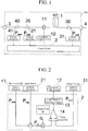
- Fig. 1 is a configuration diagram showing the configuration of an optical amplifying device 100 according to the present invention.
- the optical amplifying device 100 includes an optical transmission line having an optical amplifier that amplifies signal light inputted thereto, multiple optical element parts comprised of a light source element and optical receiving elements, and a control unit 2 that controls the components of the optical amplifying device 100.
- the optical transmission line is intended for causing signal light to propagate from an optical input unit 3 toward an optical output unit 4.
- the optical transmission line includes an optical splitter 40 that is disposed on a side closer to the optical input unit 3 and that splits light, and an optical splitter 20 at a stage following the former optical splitter.
- An optical splitter 30 that splits light is included on a side closer to the optical output unit 4. Further, an EDF (Erbium doped fiber) 1 as an amplification fiber, in the optical transmission line, which is one example of the optical amplifier is disposed between the optical splitters 20 and 30, and amplifies the signal light inputted thereto.
- the optical transmission line further includes a wavelength selective optical combiner 11, as a first irradiating unit, between the optical splitter 20 and the EDF 1.
- Signal light is inputted to the optical input unit 3. Although this input signal light is one in which multiple signal light beams having mutually different wavelengths are multiplexed, alternatively, the input signal light can be one having a single wavelength.
- the optical output unit 4 outputs the signal light amplified by the EDF 1 as output signal light. Both of the optical splitters 20 and 30 split the signal light travelling toward a forward direction from the optical input unit 3 to the optical output unit 4 to extract a part of the signal light.
- the wavelength selective optical combiner 11 combines only light beams in a specific wavelength band, and inputs combined signal light to the EDF 1.
- An excitation light source 12 includes a laser diode (LD), and it doesn't matter whether the power is fixed or variable.
- the excitation light source 12 is connected to the optical transmission line via the wavelength selective optical combiner 11, and the wavelength selective combiner 11 has a role in combining light generated by the excitation light source 12 with the signal light, and performing injection into the EDF 1.
- the excitation light source 12 amplifies the inputted signal light by applying light having a specific wavelength to the EDF 1 via the wavelength selective combiner 11.
- As the excitation light for the EDF light having a wavelength of 980 nm or 1480 nm is used generally.
- optical receivers 21, 31, and 41 include an optical receiving element.
- an optical receiving element for example, a photo diode (PD) is provided.
- the optical receiver 21 detects the power level Psig of the input signal light
- the optical receiver 31 detects the power level Pout of the output signal light
- the optical receiver 41 detects the power level Pase of backward amplified spontaneous emission noise (ASE).
- All of the optical receiving elements that constitute these optical receivers 21, 31, and 41 have a function of converting light signal into an electric signal, and convert current values acquired thereby, the current values corresponding to the light power levels, into voltage values.
- Psig, Pout, and Pase mentioned above are shown by the voltage values put into one-to-one correspondence with the light power levels.
- the control unit 2 that controls the components of the optical amplifying device 100 will be explained.
- a logical configuration diagram of the control unit 2 is shown in Fig. 2 .
- the control unit 2 adds the voltage value of Psig detected by the optical receiver 21 and the voltage value of Pase detected by the optical receiver 41 by using an adder.
- the result is multiplied by a voltage value showing a target gain G externally set up, by using a multiplier, and the result is inputted to a positive feedback terminal of an error amplifier 14.
- the voltage value of Pout detected by the optical receiver 31 is inputted to a negative feedback terminal of the error amplifier 14.
- the error amplifier generally includes an operational amplifier, and is a device that outputs a voltage corresponding to the difference between the voltages applied to the two input terminals thereof.
- the voltage signal outputted from the error amplifier 14 is inputted to a light source driving circuit 13.
- the light source driving circuit 13 generates a current or voltage being able to drive the LD of the excitation light source 12 in accordance with the output of the error amplifier 14.
- the control unit 2 can include whichever of an analog circuit and a digital circuit.
- the excitation light source driving circuit 13 is controlled in such a way that the ratio Pout/Pin of the output power level, Pout, inputted to the error amplifier 14 and the input power level, Pin, matches the target gain G.
- a gain error ⁇ G occurs notably when the input light power is low.
- Results of calculation of the operation gain against the input light power in a case in which the target gain is 18dB are shown in Fig. 3 .
- a case in which the gain error ⁇ G by ASE is equal to or less than 0.1dB is one in which the input light power is equal to or greater than -15dB.
- a result of calculation of ⁇ G is 0.04dB in a case in which the input light power corresponds to an optical signal to noise ratio (OSNR) of 20dB at input to this optical fiber amplifier. This is a permissible error for practical use.
- OSNR optical signal to noise ratio
- an optical fiber amplifier located further downstream has larger ⁇ G because accumulated ASE power is recognized as ASE power ( Fig. 4 ).
- the optical amplifying device 100 includes: the optical propagation path including the optical amplifier that amplifies input light; the excitation light source 12 that generates excitation light to excite the optical amplifier; the optical receiver 21 (referred to as a first optical receiver) that detects the power level of the input light in the optical propagation path before being amplified by the optical amplifier; the optical receiver 31 (referred to as a second optical receiver) that detects the power level of the light in the optical propagation path after being amplified by the optical amplifier; the optical receiver 41 (referred to as a third optical receiver) that detects the power level of light having a traveling direction opposite to that of the input light, in the optical propagation path; and the control unit 2 that controls the excitation light source 12 on the basis of the light power levels detected by the first, second, and third optical receivers.
- the optical propagation path including the optical amplifier that amplifies input light; the excitation light source 12 that generates excitation light to excite the optical amplifier; the optical receiver 21 (referred to as a first optical receiver) that detects the
- the input light is signal light.
- this optical amplifying device 100 can be applied to optical communications.
- the signal light is the one in which multiple signal light beams having different wavelengths are multiplexed.
- this optical amplifying device 100 can be applied to optical communications in which signals are multiplexed using different wavelengths.
- the signal light is the one in which multiple signal light beams having different wavelengths are multiplexed.
- this optical amplifying device 100 can be applied to optical communications in which signals are multiplexed using different wavelengths.
- the control unit 2 controls the excitation light source 12 in such a way that the light power level, Pout, detected by the second optical receiver approaches power (GPin+Pase) which is set on the basis of both the light power levels detected by the first and third optical receivers .
- the control unit 2 controls the excitation light source 12 in such a way that the light power level, Pout, detected by the second optical receiver approaches the light power level, Pase, detected by the third optical receiver.
- the optical propagation path has the wavelength selective combiner 11 that is disposed in a propagation path through which the input light before being amplified by the optical amplifier propagates, and that combines the excitation light generated by the excitation light source 12 with the input light before being amplified.
- the optical amplifier can be excited by the excitation light from a stage preceding the optical amplifier.
- Embodiment 2 the configuration of an optical amplifier in a case in which the arrangement of optical combining/splitting units 20 and 40 is changed with respect to Embodiment 1 will be explained.
- Fig. 5 is a configuration diagram showing the configuration of an optical amplifying device 200 according to Embodiment 2.
- the same components as those of Embodiment 1 or corresponding components are denoted by the same reference numerals, and an explanation of the components will be omitted hereafter.
- Pase is detected at a stage preceding that of detecting Psig
- the positions of detection of Pase and Psig can be interchanged, as shown in Fig. 5 .
- the optical combining/splitting units 20 and 40 are arranged in this order from a side of an optical input unit 3 with respect to an optical transmission line.
- Fig. 5 is a configuration diagram showing an embodiment in such a case.
- Embodiments 1 and 2 While in Embodiments 1 and 2, the wavelength selective optical combiner 11 and the excitation light source 12 are disposed at stages preceding the EDF 1, in Embodiment 3, a configuration in which a wavelength selective optical combiner 11 and an excitation light source 12 are disposed at stages following a EDF 1 will be explained.
- Fig. 6 is a configuration diagram showing the configuration of an optical amplifying device 300 according to Embodiment 3.
- the same components as those in Fig. 1 or corresponding components are denoted by the same reference numerals, and an explanation of the components will be omitted hereafter.
- the wavelength selective optical combiner 11 and the excitation light source 12 are disposed at stages preceding the EDF 1
- the optical amplifying device 300 according to Embodiment 3 differs in that the wavelength selective optical combiner 11 as a second optical combiner and the excitation light source 12 are disposed at stages following the EDF 1
- a wavelength selective transmitter 5 is inserted between an optical combining/splitting unit 20 and the EDF 1.
- the excitation light source 12 excites the EDF 1.
- the wavelength selective transmitter 5 has a role in removing excitation light travelling in the same direction as backward ASE, and allowing only backward ASE in a signal band to pass therethrough.
- the wavelength selective transmitter 5 is placed between the optical combining/splitting unit 20 and the EDF 1, taking its role into consideration, it is sufficient just to insert the wavelength selective transmitter between an optical receiver 41 that detects Pase and the EDF 1.
- the sequence of the optical receivers 21 and 41 and the accompanying sequence of the optical combining/splitting units 20 and 40 can be changed, like in the case of Embodiment 2.
- Embodiment 3 with the configuration of backward excitation which causes the excitation light to be combined from a stage following the EDF 1, it becomes difficult for gain saturation of signal light to occur, though noise degradation is great compared with that in the configuration of forward excitation. More specifically, higher power than that in the forward excitation which performs excitation from a stage preceding the EDF 1 by using the excitation light source 12 can be acquired.
- the wavelength selective optical combiner 11 that combines the excitation light generated by the excitation light source 12 with the input light after being amplified is provided in a propagation path through which the input light after being amplified by the optical amplifier propagates.
- an optical propagation path has the wavelength selective transmitter 5 which is an optical transmitter having wavelength selectivity, between the position of detection of light where power is detected by a third optical receiver (the position of the optical splitter 40) and the optical amplifier.
- an optical amplifier in which an excitation light source 52 as an excitation light source disposed at a stage following a EDF 1 and a wavelength selective optical combiner 51 are further included will be shown.
- Fig. 7 is a configuration diagram showing the configuration of an optical amplifying device 400 according to Embodiment 4.
- the same components as those in Fig. 1 or corresponding components are denoted by the same reference numerals, and an explanation of the components will be omitted hereafter.
- the configuration is the one in which in addition to the configuration of the optical amplifying device 100 according to Embodiment 1, the excitation light source 52 as an excitation light source disposed at a stage following the EDF 1, and the wavelength selective optical combiner 51 are further included.
- the EDF 1 is excited from both a preceding stage and the following stage. Therefore, it is possible to perform uniform excitation throughout the full length of the EDF 1.
- a wavelength selective transmitter 5 is placed between an optical combining/splitting unit 20 and a wavelength selective optical combiner 11, taking its role into consideration, it is sufficient just to insert the wavelength selective transmitter between an optical receiver 41 that detects Pase and the wavelength selective optical combiner 11.
- the sequence of optical receivers 21 and 41 and the accompanying sequence of the optical combining/splitting units 20 and 40 can be changed, like in the case of Embodiment 2.
- Embodiment 4 the optical amplifying device 400 in which the wavelength selective optical combiner 51 and the excitation light source 52 are further included at stages following the EDF 1 is shown. With this configuration, it is possible to perform uniform excitation throughout the full length of the EDF 1, and input light can be amplified efficiently.
- an optical propagation path has the wavelength selective transmitter 5 which is an optical transmitter having wavelength selectivity, between the position of detection of light where a power level is detected by a third optical receiver (the position of the optical splitter 40) and the wavelength selective optical combiner 11.
- EDF EDF
- 2 control unit
- 3 optical input unit
- 4 optical output unit
- 12, 52 excitation light source
- 13 light source driving circuit
- 14 error amplifier
- 20, 30, 40 optical splitter, 21, 31, 41: optical receiver
- 100 optical amplifying device.
Landscapes
- Physics & Mathematics (AREA)
- Electromagnetism (AREA)
- Engineering & Computer Science (AREA)
- Plasma & Fusion (AREA)
- Optics & Photonics (AREA)
- Lasers (AREA)
- Optical Communication System (AREA)
Abstract
Description
- The present invention relates to an optical amplifying device that amplifies light.
- In WDM (Wavelength Division Multiplexing) communications which implement high-capacity optical network services, an optical fiber amplifier is used in order to collectively amplify all channels of light signals whose signal strengths are attenuated because of transmission. In an optical fiber amplifier, when input signal light enters a state in which an input interruption occurs due to a transmission line fault or the like, control to cause excitation light to be emitted in a maximum emission state works in order to acquire a fixed light signal gain, even though the optical fiber amplifier is in a state in which there is no input thereto. In this case, the energy by the excitation light continues to be injected into the fiber for amplification, and the inside of the amplification fiber enters a population inversion state having high energy. A problem is that, as a result, when a light signal is inputted with restoration of the system, the population inversion state of the optical fiber amplifier changes rapidly, and this causes a light surge, so that the device at the following stage becomes damaged.
- In order to avoid this problem, control to shut down the excitation light is generally performed at the same time when an interruption of the input light signal is detected. In this control, when a decrease in the input light power level is detected, the occurrence of a light surge at the time of restoration of the input signal light is prevented by shutting down the excitation light.
- In a conventional optical fiber amplifier that prevents a light surge by shutting down excitation light, when the excitation light shutdown is canceled after restoration of input signal light, in addition to a time required to emit excitation light again, a protection time of the order of several seconds is generally required to stabilize the output level. In this case, in a system having a configuration in which optical amplifiers are connected into a multistage cascade, a time having a serious service interruption occurs. For example, in a case of a system configuration in which N optical fiber amplifiers each having a protection time of t seconds are connected into a multistage cascade, the time required to detect the input of signal light to the optical fiber amplifier at the first stage and then output the signal light amplified by the optical fiber amplifier at the final stage, starting from the state in which the excitation light beams of all the optical fiber amplifiers are shut down, is N×t seconds. In general, because t has the order of several seconds, even though an instant signal interruption occurs, an excessive time is required to perform service restoration after the network encounters the service interruption, and a serious influence is exerted on services.
- In contrast with this, in an optical fiber amplifier described in
Patent Literature 1, light (dummy light) on which no signal component is superposed is inserted into the amplification band of the optical fiber amplifier, and the power level of the dummy light is controlled in accordance with reduction in the power level of input light, as shown inFig. 8 . By thus controlling the optical amplifier in such a way that the optical amplifier is placed in a certain operating state at all times, avoidance of a shutdown is performed to avoid the occurrence of a service interruption at the same time when the occurrence of a light surge is prevented, and a light surge is prevented without causing a service interruption. - Patent Literature 1: Japanese Unexamined Patent Application Publication No.
Hei 6-152033 - A problem with the optical fiber amplifier described in
Patent Literature 1 is that because dummy light is inserted into the amplification band of the optical fiber amplifier, not the whole amplification band can be used, and the band utilization efficiency drops. For example, in a case in which the amplification band width of the optical fiber amplifier is λb [nm], and a single dummy light wave is multiplexed, a signal band permitted for WDM signals is narrowed by both λd [nm] of the dummy light and λg [nm] of the guard band for main signal channels. As a result, the bandwidth in which signal light can be inserted is λb- (λd+2λg) [nm], and the signal band permitted for WDM signals is narrowed. - The present invention is devised in order to solve the above-mentioned problem, and it is therefore an object of the present invention to implement an optical amplifying device that can use a wider amplification band than that of an optical fiber amplifier described in
Patent Literature 1. - According to the present invention, there is provided an optical amplifying device including: an optical propagation path including an optical amplifier for amplifying input light; an excitation light source for generating excitation light to excite the optical amplifier; a first optical receiver for detecting the power level of the input light in the optical propagation path before being amplified by the optical amplifier; a second optical receiver for detecting the power level of the light in the optical propagation path after being amplified by the optical amplifier; a third optical receiver for detecting the power level of light having a traveling direction opposite to that of the input light, in the optical propagation path; and a control unit for controlling the excitation light source on the basis of the light power levels detected by the first, second, and third optical receivers.
- The optical amplifying device of the present invention can use a wider amplification band than that of the optical fiber amplifier described in
Patent Literature 1. -
-
Fig. 1 is a configuration diagram showing the configuration of an opticalamplifying device 100 according toEmbodiment 1; -
Fig. 2 is a logical configuration diagram of acontrol unit 2 according toEmbodiment 1; -
Fig. 3 is a diagram showing results of calculation of an operation gain for input power inEmbodiment 1; -
Fig. 4 is a diagram showing results of calculation of ASE power against the number of amplifiers connected inEmbodiment 1. -
Fig. 5 is a configuration diagram showing the configuration of an opticalamplifying device 200 according toEmbodiment 2; -
Fig. 6 is a configuration diagram showing the configuration of an opticalamplifying device 300 according toEmbodiment 3; -
Fig. 7 is a configuration diagram showing the configuration of an opticalamplifying device 400 according toEmbodiment 4; and -
Fig. 8 is a diagram showing components in the amplification band of a conventional optical fiber amplifier. -
Fig. 1 is a configuration diagram showing the configuration of an opticalamplifying device 100 according to the present invention. InFig. 1 , the opticalamplifying device 100 includes an optical transmission line having an optical amplifier that amplifies signal light inputted thereto, multiple optical element parts comprised of a light source element and optical receiving elements, and acontrol unit 2 that controls the components of the optical amplifyingdevice 100. First, each component disposed in the optical transmission line will be explained. The optical transmission line is intended for causing signal light to propagate from anoptical input unit 3 toward anoptical output unit 4. The optical transmission line includes anoptical splitter 40 that is disposed on a side closer to theoptical input unit 3 and that splits light, and anoptical splitter 20 at a stage following the former optical splitter. Anoptical splitter 30 that splits light is included on a side closer to theoptical output unit 4. Further, an EDF (Erbium doped fiber) 1 as an amplification fiber, in the optical transmission line, which is one example of the optical amplifier is disposed between theoptical splitters optical combiner 11, as a first irradiating unit, between theoptical splitter 20 and theEDF 1. - Signal light is inputted to the
optical input unit 3. Although this input signal light is one in which multiple signal light beams having mutually different wavelengths are multiplexed, alternatively, the input signal light can be one having a single wavelength. Theoptical output unit 4 outputs the signal light amplified by the EDF 1 as output signal light. Both of theoptical splitters optical input unit 3 to theoptical output unit 4 to extract a part of the signal light. The wavelength selectiveoptical combiner 11 combines only light beams in a specific wavelength band, and inputs combined signal light to theEDF 1. - Next, the configuration of the light source element and the optical receiving elements which are shown in
Fig. 1 will be explained. Anexcitation light source 12 includes a laser diode (LD), and it doesn't matter whether the power is fixed or variable. Theexcitation light source 12 is connected to the optical transmission line via the wavelength selectiveoptical combiner 11, and the wavelengthselective combiner 11 has a role in combining light generated by theexcitation light source 12 with the signal light, and performing injection into theEDF 1. Theexcitation light source 12 amplifies the inputted signal light by applying light having a specific wavelength to theEDF 1 via the wavelengthselective combiner 11. As the excitation light for the EDF, light having a wavelength of 980 nm or 1480 nm is used generally. Further, as an impurity-doped optical fiber having a role of an amplification fiber, an optical fiber into which another rare earth element such as thulium is doped instead of erbium can be used. Each ofoptical receivers optical receiver 21 detects the power level Psig of the input signal light, theoptical receiver 31 detects the power level Pout of the output signal light, and theoptical receiver 41 detects the power level Pase of backward amplified spontaneous emission noise (ASE). All of the optical receiving elements that constitute theseoptical receivers - Next, the
control unit 2 that controls the components of the opticalamplifying device 100 will be explained. A logical configuration diagram of thecontrol unit 2 is shown inFig. 2 . Thecontrol unit 2 adds the voltage value of Psig detected by theoptical receiver 21 and the voltage value of Pase detected by theoptical receiver 41 by using an adder. The result is multiplied by a voltage value showing a target gain G externally set up, by using a multiplier, and the result is inputted to a positive feedback terminal of anerror amplifier 14. Further, the voltage value of Pout detected by theoptical receiver 31 is inputted to a negative feedback terminal of theerror amplifier 14. Here, the error amplifier generally includes an operational amplifier, and is a device that outputs a voltage corresponding to the difference between the voltages applied to the two input terminals thereof. The voltage signal outputted from theerror amplifier 14 is inputted to a lightsource driving circuit 13. The lightsource driving circuit 13 generates a current or voltage being able to drive the LD of theexcitation light source 12 in accordance with the output of theerror amplifier 14. Additionally, thecontrol unit 2 can include whichever of an analog circuit and a digital circuit. - In the
control unit 2, the excitation lightsource driving circuit 13 is controlled in such a way that the ratio Pout/Pin of the output power level, Pout, inputted to theerror amplifier 14 and the input power level, Pin, matches the target gain G. - Next, the operation of the
optical amplifying device 100 will be explained on the basis of the configurations ofFigs. 1 and 2 . - <1> At the time of a normal operation, when the power level of the input light is expressed by Psig, the target gain is expressed by G, and the power level of ASE by the optical amplifier is expressed by Pase, the power level, Pout, of the output light of the optical amplifier is expressed by an equation (1). Further, it is seen from
Fig. 2 that the input light power level, Pin, detected by the error amplifier is expressed by the sum of the input signal light power level Psig and Pase (equation (2)). Pase in the equation (2) is the power level of the backward ASE which is sent out by theamplification fiber 1 in a direction opposite to that of the signal, and generally has a value nearly equal to the power level of forward ASE. Here, Pase is much lower than Psig. In addition, nsp denotes the spontaneous emission light coefficient of the optical amplifier, h denotes the Planck constant, ν denotes the light frequency, and Δf denotes the noise bandwidth.

- <2> At the time of an input signal interruption (Psig=0), amplified ASE satisfying Pout=GPase is outputted from the amplifier. In general, while ASE is outputted bidirectionally from both ends of an amplification fiber, ASE travelling in a direction opposite to that of a signal is blocked by an optical isolator placed in the optical amplifier, which is used for prevention of laser oscillation. Here, when the operation gain of the signal except the ASE is expressed by G', the operation gain is expressed by an equation (3).

Fig. 2 , also at the time of an input signal light interruption, by providing a gain calculating unit with Pase, which is the backward ASE, as an offset, optimal excitation light power corresponding to the desired gain can be injected into the amplification fiber at all times. In the Background of the Invention, at the time of an input signal light interruption, in order to maintain a fixed gain between the input light power level and the output light power level, the excitation light enters a maximum emission state, a population inversion state having high energy is formed in the amplification fiber, and the energy is released all at once at the time of signal light restoration, so that a light surge occurs. In contrast with this, in the present invention, even at the time of a signal light interruption, the excitation light is emitted with optimal power corresponding to the target gain because an offset is added to the input light power level. It is seen from these descriptions that there does not occur a maximum emission state in which the excitation light causes a light surge at the time of signal light restoration. Further, while in the optical fiber amplifier described inPatent Literature 1, it is necessary to provide dummy light, in this embodiment, because thecontrol unit 2 performs control on the basis of the light power detected by theoptical receivers - However, because ASE is used as part of input light power, a gain error ΔG occurs notably when the input light power is low. Results of calculation of the operation gain against the input light power in a case in which the target gain is 18dB are shown in
Fig. 3 . A case in which the gain error ΔG by ASE is equal to or less than 0.1dB is one in which the input light power is equal to or greater than -15dB. For example, a result of calculation of ΔG is 0.04dB in a case in which the input light power corresponds to an optical signal to noise ratio (OSNR) of 20dB at input to this optical fiber amplifier. This is a permissible error for practical use. Further, in a case in which the backward ASE according to this embodiment is not used and the forward ASE is used as ASE by assuming that optical fiber amplifiers are connected into a multistage cascade, an optical fiber amplifier located further downstream has larger ΔG because accumulated ASE power is recognized as ASE power (Fig. 4 ). In contrast with this, because the backward ASE is used in the present invention, the power level of the ASE outputted from the optical amplifier at the time of an input signal interruption (Psig=0) is fixed to (G+1)Pase regardless of the number of optical fiber amplifiers connected. - As mentioned above, in the present invention, by using the backward ASE, a fixed-gain type optical amplifier that does not have to have a dummy light source and perform excitation light shutdown control for light surge prevention is implemented.
- As explained above, the
optical amplifying device 100 according toEmbodiment 1 includes: the optical propagation path including the optical amplifier that amplifies input light; theexcitation light source 12 that generates excitation light to excite the optical amplifier; the optical receiver 21 (referred to as a first optical receiver) that detects the power level of the input light in the optical propagation path before being amplified by the optical amplifier; the optical receiver 31 (referred to as a second optical receiver) that detects the power level of the light in the optical propagation path after being amplified by the optical amplifier; the optical receiver 41 (referred to as a third optical receiver) that detects the power level of light having a traveling direction opposite to that of the input light, in the optical propagation path; and thecontrol unit 2 that controls theexcitation light source 12 on the basis of the light power levels detected by the first, second, and third optical receivers. With this configuration, a light surge can be prevented without providing dummy light and without causing a service interruption. As a result, a wider amplification bandwidth than that of the optical fiber amplifier described inPatent Literature 1 can be used. - Further, in the
optical amplifying device 100 according toEmbodiment 1, the input light is signal light. With this configuration, thisoptical amplifying device 100 can be applied to optical communications. - Further, in the
optical amplifying device 100 according toEmbodiment 1, the signal light is the one in which multiple signal light beams having different wavelengths are multiplexed. With this configuration, thisoptical amplifying device 100 can be applied to optical communications in which signals are multiplexed using different wavelengths. - Further, in the
optical amplifying device 100 according toEmbodiment 1, the signal light is the one in which multiple signal light beams having different wavelengths are multiplexed. With this configuration, thisoptical amplifying device 100 can be applied to optical communications in which signals are multiplexed using different wavelengths. - Further, in the
optical amplifying device 100 according toEmbodiment 1, thecontrol unit 2 controls theexcitation light source 12 in such a way that the light power level, Pout, detected by the second optical receiver approaches power (GPin+Pase) which is set on the basis of both the light power levels detected by the first and third optical receivers . With this configuration, it becomes possible to control the amplification gain of the optical amplifier in such a way that the amplification gain approaches the target gain. - Further, in the
optical amplifying device 100 according toEmbodiment 1, when there exists no input light, thecontrol unit 2 controls theexcitation light source 12 in such a way that the light power level, Pout, detected by the second optical receiver approaches the light power level, Pase, detected by the third optical receiver. With this configuration, also in a case in which optical amplifiers are connected into a multistage cascade, the ASE power in the case in which there exists no input light can be maintained constant regardless of the number of optical fiber amplifiers connected. - Further, in the
optical amplifying device 100 according toEmbodiment 1, the optical propagation path has the wavelengthselective combiner 11 that is disposed in a propagation path through which the input light before being amplified by the optical amplifier propagates, and that combines the excitation light generated by theexcitation light source 12 with the input light before being amplified. With this configuration, the optical amplifier can be excited by the excitation light from a stage preceding the optical amplifier. - In
Embodiment 2, the configuration of an optical amplifier in a case in which the arrangement of optical combining/splitting units Embodiment 1 will be explained. -
Fig. 5 is a configuration diagram showing the configuration of anoptical amplifying device 200 according toEmbodiment 2. The same components as those ofEmbodiment 1 or corresponding components are denoted by the same reference numerals, and an explanation of the components will be omitted hereafter. Although inEmbodiment 1, Pase is detected at a stage preceding that of detecting Psig, the positions of detection of Pase and Psig can be interchanged, as shown inFig. 5 . More specifically, the optical combining/splitting units optical input unit 3 with respect to an optical transmission line.Fig. 5 is a configuration diagram showing an embodiment in such a case. By using this configuration, because the power level Psig of input signal light, the power level being detected by anoptical receiver 41, is not affected by an insertion loss by the optical combining/splitting unit 40, an accurate gain can be calculated. - While in
Embodiments optical combiner 11 and theexcitation light source 12 are disposed at stages preceding theEDF 1, inEmbodiment 3, a configuration in which a wavelength selectiveoptical combiner 11 and anexcitation light source 12 are disposed at stages following aEDF 1 will be explained. -
Fig. 6 is a configuration diagram showing the configuration of anoptical amplifying device 300 according toEmbodiment 3. The same components as those inFig. 1 or corresponding components are denoted by the same reference numerals, and an explanation of the components will be omitted hereafter. While in theoptical amplifying device 100 according toEmbodiment 1, the wavelength selectiveoptical combiner 11 and theexcitation light source 12 are disposed at stages preceding theEDF 1, theoptical amplifying device 300 according toEmbodiment 3 differs in that the wavelength selectiveoptical combiner 11 as a second optical combiner and theexcitation light source 12 are disposed at stages following theEDF 1, and a wavelengthselective transmitter 5 is inserted between an optical combining/splitting unit 20 and theEDF 1. In this case, at a stage following theEDF 1, theexcitation light source 12 excites theEDF 1. Further, the wavelengthselective transmitter 5 has a role in removing excitation light travelling in the same direction as backward ASE, and allowing only backward ASE in a signal band to pass therethrough. Although inFig. 6 , the wavelengthselective transmitter 5 is placed between the optical combining/splitting unit 20 and theEDF 1, taking its role into consideration, it is sufficient just to insert the wavelength selective transmitter between anoptical receiver 41 that detects Pase and theEDF 1. In addition, it is needless to say that the sequence of theoptical receivers splitting units Embodiment 2. - In
Embodiment 3, with the configuration of backward excitation which causes the excitation light to be combined from a stage following theEDF 1, it becomes difficult for gain saturation of signal light to occur, though noise degradation is great compared with that in the configuration of forward excitation. More specifically, higher power than that in the forward excitation which performs excitation from a stage preceding theEDF 1 by using theexcitation light source 12 can be acquired. - More specifically, in the
optical amplifying device 300 according toEmbodiment 3, the wavelength selectiveoptical combiner 11 that combines the excitation light generated by theexcitation light source 12 with the input light after being amplified is provided in a propagation path through which the input light after being amplified by the optical amplifier propagates. With this configuration, higher power than that in the forward excitation which performs excitation from a stage preceding theEDF 1 by using theexcitation light source 12 can be acquired. - Further, in the
optical amplifying device 300 according toEmbodiment 3, an optical propagation path has the wavelengthselective transmitter 5 which is an optical transmitter having wavelength selectivity, between the position of detection of light where power is detected by a third optical receiver (the position of the optical splitter 40) and the optical amplifier. With this configuration, the excitation light travelling in the same direction as the backward ASE can be removed, and only the backward ASE in the signal band can be allowed to pass. - In this embodiment, the configuration of an optical amplifier in which an
excitation light source 52 as an excitation light source disposed at a stage following aEDF 1 and a wavelength selectiveoptical combiner 51 are further included will be shown. -
Fig. 7 is a configuration diagram showing the configuration of anoptical amplifying device 400 according toEmbodiment 4. The same components as those inFig. 1 or corresponding components are denoted by the same reference numerals, and an explanation of the components will be omitted hereafter. The configuration is the one in which in addition to the configuration of theoptical amplifying device 100 according toEmbodiment 1, theexcitation light source 52 as an excitation light source disposed at a stage following theEDF 1, and the wavelength selectiveoptical combiner 51 are further included. TheEDF 1 is excited from both a preceding stage and the following stage. Therefore, it is possible to perform uniform excitation throughout the full length of theEDF 1. Although inFig. 7 , a wavelengthselective transmitter 5 is placed between an optical combining/splitting unit 20 and a wavelength selectiveoptical combiner 11, taking its role into consideration, it is sufficient just to insert the wavelength selective transmitter between anoptical receiver 41 that detects Pase and the wavelength selectiveoptical combiner 11. In addition, it is needless to say that the sequence ofoptical receivers splitting units Embodiment 2. - In
Embodiment 4, theoptical amplifying device 400 in which the wavelength selectiveoptical combiner 51 and theexcitation light source 52 are further included at stages following theEDF 1 is shown. With this configuration, it is possible to perform uniform excitation throughout the full length of theEDF 1, and input light can be amplified efficiently. - Further, in the
optical amplifying device 400 according toEmbodiment 4, an optical propagation path has the wavelengthselective transmitter 5 which is an optical transmitter having wavelength selectivity, between the position of detection of light where a power level is detected by a third optical receiver (the position of the optical splitter 40) and the wavelength selectiveoptical combiner 11. With this configuration, excitation light travelling in the same direction as backward ASE can be removed, and only backward ASE in a signal band can be allowed to pass. - 1: EDF, 2: control unit, 3: optical input unit, 4: optical output unit, 11, 51: wavelength selective combiner, 12, 52: excitation light source, 13: light source driving circuit, 14: error amplifier, 20, 30, 40: optical splitter, 21, 31, 41: optical receiver, and 100: optical amplifying device.
Claims (9)
- An optical amplifying device comprising:an optical propagation path including an optical amplifier to amplify input light;an excitation light source to generate excitation light to excite the optical amplifier;a first optical receiver to detect power of the input light in the optical propagation path before being amplified by the optical amplifier;a second optical receiver to detect power of light in the optical propagation path after being amplified by the optical amplifier;a third optical receiver to detect power of light having a traveling direction opposite to that of the input light, in the optical propagation path; anda controller to control the excitation light source on a basis of light power detected by the first optical receiver, light power detected by the second optical receiver, and light power detected by the third optical receiver.
- The optical amplifying device according to claim 1, wherein the input light is signal light.
- The optical amplifying device according to claim 1, wherein the input light is signal light in which multiple signal light beams having different wavelengths are multiplexed.
- The optical amplifying device according to any one of claims 1 to 3, wherein the controller controls the excitation light source in such a way that the light power detected by the second optical receiver approaches power which is set on a basis of both the light power detected by the first optical receiver and the light power detected by the third optical receiver.
- The optical amplifying device according to any one of claims 1 to 4, wherein when the input light does not exist, the controller controls the excitation light source in such a way that the light power detected by the second optical receiver approaches the light power detected by the third optical receiver.
- The optical amplifying device according to any one of claims 1 to 5, wherein the optical propagation path has a combiner to combine the excitation light and the input light in a propagation path through which the input light before being amplified by the optical amplifier propagates.
- The optical amplifying device according to any one of claims 1 to 6, wherein the optical propagation path has a combiner to combine the excitation light and the input light after being amplified by the optical amplifier in a propagation path through which the input light after being amplified by the optical amplifier propagates.
- The optical amplifying device according to any one of claims 1 to 7, wherein the optical propagation path has an optical transmitter between a position where the power of the light is detected by the third optical receiver, and the optical amplifier.
- The optical amplifying device according to claim 6, wherein the optical propagation path has an optical transmitter between a position where the power of the light is detected by the third optical receiver, and the combiner.
Applications Claiming Priority (1)
| Application Number | Priority Date | Filing Date | Title |
|---|---|---|---|
| PCT/JP2016/064238 WO2017195341A1 (en) | 2016-05-13 | 2016-05-13 | Optical amplification device |
Publications (3)
| Publication Number | Publication Date |
|---|---|
| EP3447861A1 true EP3447861A1 (en) | 2019-02-27 |
| EP3447861A4 EP3447861A4 (en) | 2019-04-24 |
| EP3447861B1 EP3447861B1 (en) | 2020-04-22 |
Family
ID=59366049
Family Applications (1)
| Application Number | Title | Priority Date | Filing Date |
|---|---|---|---|
| EP16901689.6A Active EP3447861B1 (en) | 2016-05-13 | 2016-05-13 | Optical amplification device |
Country Status (5)
| Country | Link |
|---|---|
| US (1) | US11196226B2 (en) |
| EP (1) | EP3447861B1 (en) |
| JP (1) | JP6103159B1 (en) |
| CN (1) | CN109075521A (en) |
| WO (1) | WO2017195341A1 (en) |
Families Citing this family (1)
| Publication number | Priority date | Publication date | Assignee | Title |
|---|---|---|---|---|
| WO2025234277A1 (en) * | 2024-05-07 | 2025-11-13 | 株式会社フジクラ | Laser device |
Family Cites Families (10)
| Publication number | Priority date | Publication date | Assignee | Title |
|---|---|---|---|---|
| JPH06152033A (en) | 1992-11-02 | 1994-05-31 | Nec Corp | Optical amplifier |
| JP3808580B2 (en) * | 1997-03-17 | 2006-08-16 | 富士通株式会社 | Optical power monitor and optical amplifier having the optical power monitor |
| JPH11112435A (en) * | 1997-10-07 | 1999-04-23 | Fujitsu Ltd | Optical amplifier |
| EP1273077A1 (en) * | 2000-04-13 | 2003-01-08 | Siemens Aktiengesellschaft | Method and device for regulating a medium with an amplifying effect, especially a fiber optical waveguide |
| JP2001352119A (en) * | 2000-06-08 | 2001-12-21 | Mitsubishi Electric Corp | Optical amplifier |
| JP3904835B2 (en) * | 2001-01-29 | 2007-04-11 | 株式会社日立製作所 | Optical amplifier, optical fiber Raman optical amplifier, and optical system |
| US20030142388A1 (en) * | 2002-01-31 | 2003-07-31 | Sergey Frolov | Waveguide optical amplifier |
| JP2003347633A (en) * | 2003-04-21 | 2003-12-05 | Fujitsu Ltd | Optical amplifier |
| JP2006269855A (en) * | 2005-03-25 | 2006-10-05 | Central Glass Co Ltd | Optical fiber amplifier |
| JP4648263B2 (en) | 2006-07-21 | 2011-03-09 | 株式会社日立製作所 | Optical amplifier and optical transmission device |
-
2016
- 2016-05-13 US US16/094,720 patent/US11196226B2/en active Active
- 2016-05-13 WO PCT/JP2016/064238 patent/WO2017195341A1/en not_active Ceased
- 2016-05-13 EP EP16901689.6A patent/EP3447861B1/en active Active
- 2016-05-13 JP JP2016563149A patent/JP6103159B1/en active Active
- 2016-05-13 CN CN201680085409.5A patent/CN109075521A/en active Pending
Also Published As
| Publication number | Publication date |
|---|---|
| US20200235545A1 (en) | 2020-07-23 |
| CN109075521A (en) | 2018-12-21 |
| EP3447861A4 (en) | 2019-04-24 |
| JP6103159B1 (en) | 2017-03-29 |
| WO2017195341A1 (en) | 2017-11-16 |
| EP3447861B1 (en) | 2020-04-22 |
| US11196226B2 (en) | 2021-12-07 |
| JPWO2017195341A1 (en) | 2018-05-24 |
Similar Documents
| Publication | Publication Date | Title |
|---|---|---|
| JPH08304856A (en) | Optical fiber amplifier | |
| JPH08304859A (en) | Optical fiber amplifier | |
| JPH11112434A (en) | Optical fiber amplifier | |
| US7142356B2 (en) | Fast dynamic gain control in an optical fiber amplifier | |
| US6339494B1 (en) | Gain flattened optical fiber amplifier | |
| JP4198082B2 (en) | Optical amplifier gain monitoring method and apparatus | |
| JPH09214034A (en) | Optical amplifier | |
| EP3447861B1 (en) | Optical amplification device | |
| JPH1022556A (en) | Optical gain control type optical amplifier | |
| JP3893963B2 (en) | Optical amplifier and optical communication system | |
| US20060187538A1 (en) | Fast dynamic gain control in an optical fiber amplifier | |
| WO2011026502A1 (en) | Optical fiber amplifier compromising an embedded filter and a control method with improved feedforward control performance | |
| EP0959640B1 (en) | Optical switch and optical network | |
| JP3567451B2 (en) | Optical amplifier | |
| EP1696524B1 (en) | Fast dynamic gain control in an optical fiber amplifier | |
| JPH09107141A (en) | Optical amplifier | |
| JP2714611B2 (en) | Optical repeater and optical transmission network using the same | |
| JP2001036174A (en) | Optical amplifier | |
| JP3111975B2 (en) | Optical fiber amplifier, optical transmitter and optical receiver having the same | |
| JP6366257B2 (en) | Optical amplification apparatus, optical communication system, and optical amplification method | |
| JP4133951B2 (en) | Method for estimating input light intensity of optical amplifier and optical amplifier | |
| JP3940926B2 (en) | Wavelength multiplexed optical amplifier | |
| JP3551419B2 (en) | Optical transmission device and wavelength division multiplexing optical communication system | |
| EP1058413A2 (en) | Gain-flattening optical amplifier | |
| JP2025117782A (en) | Optical amplifier and optical amplifier monitoring method |
Legal Events
| Date | Code | Title | Description |
|---|---|---|---|
| STAA | Information on the status of an ep patent application or granted ep patent |
Free format text: STATUS: THE INTERNATIONAL PUBLICATION HAS BEEN MADE |
|
| PUAI | Public reference made under article 153(3) epc to a published international application that has entered the european phase |
Free format text: ORIGINAL CODE: 0009012 |
|
| STAA | Information on the status of an ep patent application or granted ep patent |
Free format text: STATUS: REQUEST FOR EXAMINATION WAS MADE |
|
| 17P | Request for examination filed |
Effective date: 20181107 |
|
| AK | Designated contracting states |
Kind code of ref document: A1 Designated state(s): AL AT BE BG CH CY CZ DE DK EE ES FI FR GB GR HR HU IE IS IT LI LT LU LV MC MK MT NL NO PL PT RO RS SE SI SK SM TR |
|
| AX | Request for extension of the european patent |
Extension state: BA ME |
|
| A4 | Supplementary search report drawn up and despatched |
Effective date: 20190321 |
|
| RIC1 | Information provided on ipc code assigned before grant |
Ipc: H01S 3/067 20060101AFI20190315BHEP Ipc: H01S 3/16 20060101ALI20190315BHEP Ipc: H01S 3/094 20060101ALI20190315BHEP Ipc: H01S 3/13 20060101ALI20190315BHEP Ipc: H01S 3/00 20060101ALI20190315BHEP Ipc: H01S 3/0941 20060101ALI20190315BHEP Ipc: H01S 3/10 20060101ALI20190315BHEP |
|
| DAV | Request for validation of the european patent (deleted) | ||
| DAX | Request for extension of the european patent (deleted) | ||
| GRAP | Despatch of communication of intention to grant a patent |
Free format text: ORIGINAL CODE: EPIDOSNIGR1 |
|
| STAA | Information on the status of an ep patent application or granted ep patent |
Free format text: STATUS: GRANT OF PATENT IS INTENDED |
|
| INTG | Intention to grant announced |
Effective date: 20191122 |
|
| GRAS | Grant fee paid |
Free format text: ORIGINAL CODE: EPIDOSNIGR3 |
|
| GRAA | (expected) grant |
Free format text: ORIGINAL CODE: 0009210 |
|
| STAA | Information on the status of an ep patent application or granted ep patent |
Free format text: STATUS: THE PATENT HAS BEEN GRANTED |
|
| AK | Designated contracting states |
Kind code of ref document: B1 Designated state(s): AL AT BE BG CH CY CZ DE DK EE ES FI FR GB GR HR HU IE IS IT LI LT LU LV MC MK MT NL NO PL PT RO RS SE SI SK SM TR |
|
| REG | Reference to a national code |
Ref country code: CH Ref legal event code: EP |
|
| REG | Reference to a national code |
Ref country code: IE Ref legal event code: FG4D |
|
| REG | Reference to a national code |
Ref country code: DE Ref legal event code: R096 Ref document number: 602016034844 Country of ref document: DE |
|
| REG | Reference to a national code |
Ref country code: AT Ref legal event code: REF Ref document number: 1261394 Country of ref document: AT Kind code of ref document: T Effective date: 20200515 |
|
| REG | Reference to a national code |
Ref country code: LT Ref legal event code: MG4D |
|
| REG | Reference to a national code |
Ref country code: NL Ref legal event code: MP Effective date: 20200422 |
|
| PG25 | Lapsed in a contracting state [announced via postgrant information from national office to epo] |
Ref country code: IS Free format text: LAPSE BECAUSE OF FAILURE TO SUBMIT A TRANSLATION OF THE DESCRIPTION OR TO PAY THE FEE WITHIN THE PRESCRIBED TIME-LIMIT Effective date: 20200822 Ref country code: NO Free format text: LAPSE BECAUSE OF FAILURE TO SUBMIT A TRANSLATION OF THE DESCRIPTION OR TO PAY THE FEE WITHIN THE PRESCRIBED TIME-LIMIT Effective date: 20200722 Ref country code: GR Free format text: LAPSE BECAUSE OF FAILURE TO SUBMIT A TRANSLATION OF THE DESCRIPTION OR TO PAY THE FEE WITHIN THE PRESCRIBED TIME-LIMIT Effective date: 20200723 Ref country code: FI Free format text: LAPSE BECAUSE OF FAILURE TO SUBMIT A TRANSLATION OF THE DESCRIPTION OR TO PAY THE FEE WITHIN THE PRESCRIBED TIME-LIMIT Effective date: 20200422 Ref country code: SE Free format text: LAPSE BECAUSE OF FAILURE TO SUBMIT A TRANSLATION OF THE DESCRIPTION OR TO PAY THE FEE WITHIN THE PRESCRIBED TIME-LIMIT Effective date: 20200422 Ref country code: LT Free format text: LAPSE BECAUSE OF FAILURE TO SUBMIT A TRANSLATION OF THE DESCRIPTION OR TO PAY THE FEE WITHIN THE PRESCRIBED TIME-LIMIT Effective date: 20200422 Ref country code: PT Free format text: LAPSE BECAUSE OF FAILURE TO SUBMIT A TRANSLATION OF THE DESCRIPTION OR TO PAY THE FEE WITHIN THE PRESCRIBED TIME-LIMIT Effective date: 20200824 Ref country code: NL Free format text: LAPSE BECAUSE OF FAILURE TO SUBMIT A TRANSLATION OF THE DESCRIPTION OR TO PAY THE FEE WITHIN THE PRESCRIBED TIME-LIMIT Effective date: 20200422 |
|
| REG | Reference to a national code |
Ref country code: AT Ref legal event code: MK05 Ref document number: 1261394 Country of ref document: AT Kind code of ref document: T Effective date: 20200422 |
|
| PG25 | Lapsed in a contracting state [announced via postgrant information from national office to epo] |
Ref country code: BG Free format text: LAPSE BECAUSE OF FAILURE TO SUBMIT A TRANSLATION OF THE DESCRIPTION OR TO PAY THE FEE WITHIN THE PRESCRIBED TIME-LIMIT Effective date: 20200722 Ref country code: RS Free format text: LAPSE BECAUSE OF FAILURE TO SUBMIT A TRANSLATION OF THE DESCRIPTION OR TO PAY THE FEE WITHIN THE PRESCRIBED TIME-LIMIT Effective date: 20200422 Ref country code: LV Free format text: LAPSE BECAUSE OF FAILURE TO SUBMIT A TRANSLATION OF THE DESCRIPTION OR TO PAY THE FEE WITHIN THE PRESCRIBED TIME-LIMIT Effective date: 20200422 Ref country code: HR Free format text: LAPSE BECAUSE OF FAILURE TO SUBMIT A TRANSLATION OF THE DESCRIPTION OR TO PAY THE FEE WITHIN THE PRESCRIBED TIME-LIMIT Effective date: 20200422 |
|
| REG | Reference to a national code |
Ref country code: DE Ref legal event code: R119 Ref document number: 602016034844 Country of ref document: DE |
|
| PG25 | Lapsed in a contracting state [announced via postgrant information from national office to epo] |
Ref country code: AL Free format text: LAPSE BECAUSE OF FAILURE TO SUBMIT A TRANSLATION OF THE DESCRIPTION OR TO PAY THE FEE WITHIN THE PRESCRIBED TIME-LIMIT Effective date: 20200422 |
|
| PG25 | Lapsed in a contracting state [announced via postgrant information from national office to epo] |
Ref country code: AT Free format text: LAPSE BECAUSE OF FAILURE TO SUBMIT A TRANSLATION OF THE DESCRIPTION OR TO PAY THE FEE WITHIN THE PRESCRIBED TIME-LIMIT Effective date: 20200422 Ref country code: LI Free format text: LAPSE BECAUSE OF NON-PAYMENT OF DUE FEES Effective date: 20200531 Ref country code: MC Free format text: LAPSE BECAUSE OF FAILURE TO SUBMIT A TRANSLATION OF THE DESCRIPTION OR TO PAY THE FEE WITHIN THE PRESCRIBED TIME-LIMIT Effective date: 20200422 Ref country code: EE Free format text: LAPSE BECAUSE OF FAILURE TO SUBMIT A TRANSLATION OF THE DESCRIPTION OR TO PAY THE FEE WITHIN THE PRESCRIBED TIME-LIMIT Effective date: 20200422 Ref country code: SM Free format text: LAPSE BECAUSE OF FAILURE TO SUBMIT A TRANSLATION OF THE DESCRIPTION OR TO PAY THE FEE WITHIN THE PRESCRIBED TIME-LIMIT Effective date: 20200422 Ref country code: DK Free format text: LAPSE BECAUSE OF FAILURE TO SUBMIT A TRANSLATION OF THE DESCRIPTION OR TO PAY THE FEE WITHIN THE PRESCRIBED TIME-LIMIT Effective date: 20200422 Ref country code: CH Free format text: LAPSE BECAUSE OF NON-PAYMENT OF DUE FEES Effective date: 20200531 Ref country code: RO Free format text: LAPSE BECAUSE OF FAILURE TO SUBMIT A TRANSLATION OF THE DESCRIPTION OR TO PAY THE FEE WITHIN THE PRESCRIBED TIME-LIMIT Effective date: 20200422 Ref country code: IT Free format text: LAPSE BECAUSE OF FAILURE TO SUBMIT A TRANSLATION OF THE DESCRIPTION OR TO PAY THE FEE WITHIN THE PRESCRIBED TIME-LIMIT Effective date: 20200422 Ref country code: CZ Free format text: LAPSE BECAUSE OF FAILURE TO SUBMIT A TRANSLATION OF THE DESCRIPTION OR TO PAY THE FEE WITHIN THE PRESCRIBED TIME-LIMIT Effective date: 20200422 Ref country code: ES Free format text: LAPSE BECAUSE OF FAILURE TO SUBMIT A TRANSLATION OF THE DESCRIPTION OR TO PAY THE FEE WITHIN THE PRESCRIBED TIME-LIMIT Effective date: 20200422 |
|
| PG25 | Lapsed in a contracting state [announced via postgrant information from national office to epo] |
Ref country code: PL Free format text: LAPSE BECAUSE OF FAILURE TO SUBMIT A TRANSLATION OF THE DESCRIPTION OR TO PAY THE FEE WITHIN THE PRESCRIBED TIME-LIMIT Effective date: 20200422 Ref country code: SK Free format text: LAPSE BECAUSE OF FAILURE TO SUBMIT A TRANSLATION OF THE DESCRIPTION OR TO PAY THE FEE WITHIN THE PRESCRIBED TIME-LIMIT Effective date: 20200422 |
|
| PLBE | No opposition filed within time limit |
Free format text: ORIGINAL CODE: 0009261 |
|
| STAA | Information on the status of an ep patent application or granted ep patent |
Free format text: STATUS: NO OPPOSITION FILED WITHIN TIME LIMIT |
|
| REG | Reference to a national code |
Ref country code: BE Ref legal event code: MM Effective date: 20200531 |
|
| 26N | No opposition filed |
Effective date: 20210125 |
|
| GBPC | Gb: european patent ceased through non-payment of renewal fee |
Effective date: 20200722 |
|
| PG25 | Lapsed in a contracting state [announced via postgrant information from national office to epo] |
Ref country code: LU Free format text: LAPSE BECAUSE OF NON-PAYMENT OF DUE FEES Effective date: 20200513 |
|
| PG25 | Lapsed in a contracting state [announced via postgrant information from national office to epo] |
Ref country code: IE Free format text: LAPSE BECAUSE OF NON-PAYMENT OF DUE FEES Effective date: 20200513 Ref country code: GB Free format text: LAPSE BECAUSE OF NON-PAYMENT OF DUE FEES Effective date: 20200722 |
|
| PG25 | Lapsed in a contracting state [announced via postgrant information from national office to epo] |
Ref country code: SI Free format text: LAPSE BECAUSE OF FAILURE TO SUBMIT A TRANSLATION OF THE DESCRIPTION OR TO PAY THE FEE WITHIN THE PRESCRIBED TIME-LIMIT Effective date: 20200422 Ref country code: BE Free format text: LAPSE BECAUSE OF NON-PAYMENT OF DUE FEES Effective date: 20200531 Ref country code: DE Free format text: LAPSE BECAUSE OF NON-PAYMENT OF DUE FEES Effective date: 20201201 |
|
| PG25 | Lapsed in a contracting state [announced via postgrant information from national office to epo] |
Ref country code: TR Free format text: LAPSE BECAUSE OF FAILURE TO SUBMIT A TRANSLATION OF THE DESCRIPTION OR TO PAY THE FEE WITHIN THE PRESCRIBED TIME-LIMIT Effective date: 20200422 Ref country code: MT Free format text: LAPSE BECAUSE OF FAILURE TO SUBMIT A TRANSLATION OF THE DESCRIPTION OR TO PAY THE FEE WITHIN THE PRESCRIBED TIME-LIMIT Effective date: 20200422 Ref country code: CY Free format text: LAPSE BECAUSE OF FAILURE TO SUBMIT A TRANSLATION OF THE DESCRIPTION OR TO PAY THE FEE WITHIN THE PRESCRIBED TIME-LIMIT Effective date: 20200422 |
|
| PG25 | Lapsed in a contracting state [announced via postgrant information from national office to epo] |
Ref country code: MK Free format text: LAPSE BECAUSE OF FAILURE TO SUBMIT A TRANSLATION OF THE DESCRIPTION OR TO PAY THE FEE WITHIN THE PRESCRIBED TIME-LIMIT Effective date: 20200422 |
|
| P01 | Opt-out of the competence of the unified patent court (upc) registered |
Effective date: 20230512 |
|
| PGFP | Annual fee paid to national office [announced via postgrant information from national office to epo] |
Ref country code: FR Payment date: 20250401 Year of fee payment: 10 |