EP3447795A1 - Molded wafer level packaging - Google Patents
Molded wafer level packaging Download PDFInfo
- Publication number
- EP3447795A1 EP3447795A1 EP18183293.2A EP18183293A EP3447795A1 EP 3447795 A1 EP3447795 A1 EP 3447795A1 EP 18183293 A EP18183293 A EP 18183293A EP 3447795 A1 EP3447795 A1 EP 3447795A1
- Authority
- EP
- European Patent Office
- Prior art keywords
- semiconductor die
- electrical contact
- metal layer
- semiconductor
- disposed
- Prior art date
- Legal status (The legal status is an assumption and is not a legal conclusion. Google has not performed a legal analysis and makes no representation as to the accuracy of the status listed.)
- Granted
Links
Images



Classifications
-
- H—ELECTRICITY
- H10—SEMICONDUCTOR DEVICES; ELECTRIC SOLID-STATE DEVICES NOT OTHERWISE PROVIDED FOR
- H10W—GENERIC PACKAGES, INTERCONNECTIONS, CONNECTORS OR OTHER CONSTRUCTIONAL DETAILS OF DEVICES COVERED BY CLASS H10
- H10W74/00—Encapsulations, e.g. protective coatings
- H10W74/10—Encapsulations, e.g. protective coatings characterised by their shape or disposition
- H10W74/111—Encapsulations, e.g. protective coatings characterised by their shape or disposition the semiconductor body being completely enclosed
- H10W74/129—Encapsulations, e.g. protective coatings characterised by their shape or disposition the semiconductor body being completely enclosed forming a chip-scale package [CSP]
-
- H—ELECTRICITY
- H10—SEMICONDUCTOR DEVICES; ELECTRIC SOLID-STATE DEVICES NOT OTHERWISE PROVIDED FOR
- H10P—GENERIC PROCESSES OR APPARATUS FOR THE MANUFACTURE OR TREATMENT OF DEVICES COVERED BY CLASS H10
- H10P54/00—Cutting or separating of wafers, substrates or parts of devices
-
- H—ELECTRICITY
- H10—SEMICONDUCTOR DEVICES; ELECTRIC SOLID-STATE DEVICES NOT OTHERWISE PROVIDED FOR
- H10P—GENERIC PROCESSES OR APPARATUS FOR THE MANUFACTURE OR TREATMENT OF DEVICES COVERED BY CLASS H10
- H10P95/00—Generic processes or apparatus for manufacture or treatments not covered by the other groups of this subclass
- H10P95/06—Planarisation of inorganic insulating materials
- H10P95/062—Planarisation of inorganic insulating materials involving a dielectric removal step
-
- H—ELECTRICITY
- H10—SEMICONDUCTOR DEVICES; ELECTRIC SOLID-STATE DEVICES NOT OTHERWISE PROVIDED FOR
- H10W—GENERIC PACKAGES, INTERCONNECTIONS, CONNECTORS OR OTHER CONSTRUCTIONAL DETAILS OF DEVICES COVERED BY CLASS H10
- H10W70/00—Package substrates; Interposers; Redistribution layers [RDL]
- H10W70/20—Conductive package substrates serving as an interconnection, e.g. metal plates
-
- H—ELECTRICITY
- H10—SEMICONDUCTOR DEVICES; ELECTRIC SOLID-STATE DEVICES NOT OTHERWISE PROVIDED FOR
- H10W—GENERIC PACKAGES, INTERCONNECTIONS, CONNECTORS OR OTHER CONSTRUCTIONAL DETAILS OF DEVICES COVERED BY CLASS H10
- H10W72/00—Interconnections or connectors in packages
- H10W72/01—Manufacture or treatment
- H10W72/012—Manufacture or treatment of bump connectors, dummy bumps or thermal bumps
-
- H—ELECTRICITY
- H10—SEMICONDUCTOR DEVICES; ELECTRIC SOLID-STATE DEVICES NOT OTHERWISE PROVIDED FOR
- H10W—GENERIC PACKAGES, INTERCONNECTIONS, CONNECTORS OR OTHER CONSTRUCTIONAL DETAILS OF DEVICES COVERED BY CLASS H10
- H10W74/00—Encapsulations, e.g. protective coatings
- H10W74/01—Manufacture or treatment
- H10W74/014—Manufacture or treatment using batch processing
-
- H—ELECTRICITY
- H10—SEMICONDUCTOR DEVICES; ELECTRIC SOLID-STATE DEVICES NOT OTHERWISE PROVIDED FOR
- H10W—GENERIC PACKAGES, INTERCONNECTIONS, CONNECTORS OR OTHER CONSTRUCTIONAL DETAILS OF DEVICES COVERED BY CLASS H10
- H10W74/00—Encapsulations, e.g. protective coatings
- H10W74/01—Manufacture or treatment
- H10W74/016—Manufacture or treatment using moulds
-
- H—ELECTRICITY
- H10—SEMICONDUCTOR DEVICES; ELECTRIC SOLID-STATE DEVICES NOT OTHERWISE PROVIDED FOR
- H10W—GENERIC PACKAGES, INTERCONNECTIONS, CONNECTORS OR OTHER CONSTRUCTIONAL DETAILS OF DEVICES COVERED BY CLASS H10
- H10W74/00—Encapsulations, e.g. protective coatings
- H10W74/10—Encapsulations, e.g. protective coatings characterised by their shape or disposition
- H10W74/111—Encapsulations, e.g. protective coatings characterised by their shape or disposition the semiconductor body being completely enclosed
-
- H—ELECTRICITY
- H10—SEMICONDUCTOR DEVICES; ELECTRIC SOLID-STATE DEVICES NOT OTHERWISE PROVIDED FOR
- H10W—GENERIC PACKAGES, INTERCONNECTIONS, CONNECTORS OR OTHER CONSTRUCTIONAL DETAILS OF DEVICES COVERED BY CLASS H10
- H10W90/00—Package configurations
-
- H—ELECTRICITY
- H10—SEMICONDUCTOR DEVICES; ELECTRIC SOLID-STATE DEVICES NOT OTHERWISE PROVIDED FOR
- H10W—GENERIC PACKAGES, INTERCONNECTIONS, CONNECTORS OR OTHER CONSTRUCTIONAL DETAILS OF DEVICES COVERED BY CLASS H10
- H10W70/00—Package substrates; Interposers; Redistribution layers [RDL]
- H10W70/40—Leadframes
- H10W70/481—Leadframes for devices being provided for in groups H10D8/00 - H10D48/00
-
- H—ELECTRICITY
- H10—SEMICONDUCTOR DEVICES; ELECTRIC SOLID-STATE DEVICES NOT OTHERWISE PROVIDED FOR
- H10W—GENERIC PACKAGES, INTERCONNECTIONS, CONNECTORS OR OTHER CONSTRUCTIONAL DETAILS OF DEVICES COVERED BY CLASS H10
- H10W72/00—Interconnections or connectors in packages
- H10W72/01—Manufacture or treatment
- H10W72/019—Manufacture or treatment of bond pads
-
- H—ELECTRICITY
- H10—SEMICONDUCTOR DEVICES; ELECTRIC SOLID-STATE DEVICES NOT OTHERWISE PROVIDED FOR
- H10W—GENERIC PACKAGES, INTERCONNECTIONS, CONNECTORS OR OTHER CONSTRUCTIONAL DETAILS OF DEVICES COVERED BY CLASS H10
- H10W72/00—Interconnections or connectors in packages
- H10W72/01—Manufacture or treatment
- H10W72/0198—Manufacture or treatment batch processes
-
- H—ELECTRICITY
- H10—SEMICONDUCTOR DEVICES; ELECTRIC SOLID-STATE DEVICES NOT OTHERWISE PROVIDED FOR
- H10W—GENERIC PACKAGES, INTERCONNECTIONS, CONNECTORS OR OTHER CONSTRUCTIONAL DETAILS OF DEVICES COVERED BY CLASS H10
- H10W72/00—Interconnections or connectors in packages
- H10W72/20—Bump connectors, e.g. solder bumps or copper pillars; Dummy bumps; Thermal bumps
- H10W72/241—Dispositions, e.g. layouts
- H10W72/242—Dispositions, e.g. layouts relative to the surface, e.g. recessed, protruding
-
- H—ELECTRICITY
- H10—SEMICONDUCTOR DEVICES; ELECTRIC SOLID-STATE DEVICES NOT OTHERWISE PROVIDED FOR
- H10W—GENERIC PACKAGES, INTERCONNECTIONS, CONNECTORS OR OTHER CONSTRUCTIONAL DETAILS OF DEVICES COVERED BY CLASS H10
- H10W72/00—Interconnections or connectors in packages
- H10W72/20—Bump connectors, e.g. solder bumps or copper pillars; Dummy bumps; Thermal bumps
- H10W72/251—Materials
- H10W72/252—Materials comprising solid metals or solid metalloids, e.g. PbSn, Ag or Cu
-
- H—ELECTRICITY
- H10—SEMICONDUCTOR DEVICES; ELECTRIC SOLID-STATE DEVICES NOT OTHERWISE PROVIDED FOR
- H10W—GENERIC PACKAGES, INTERCONNECTIONS, CONNECTORS OR OTHER CONSTRUCTIONAL DETAILS OF DEVICES COVERED BY CLASS H10
- H10W72/00—Interconnections or connectors in packages
- H10W72/851—Dispositions of multiple connectors or interconnections
- H10W72/853—On the same surface
- H10W72/856—Bump connectors and die-attach connectors
-
- H—ELECTRICITY
- H10—SEMICONDUCTOR DEVICES; ELECTRIC SOLID-STATE DEVICES NOT OTHERWISE PROVIDED FOR
- H10W—GENERIC PACKAGES, INTERCONNECTIONS, CONNECTORS OR OTHER CONSTRUCTIONAL DETAILS OF DEVICES COVERED BY CLASS H10
- H10W72/00—Interconnections or connectors in packages
- H10W72/851—Dispositions of multiple connectors or interconnections
- H10W72/874—On different surfaces
- H10W72/877—Bump connectors and die-attach connectors
-
- H—ELECTRICITY
- H10—SEMICONDUCTOR DEVICES; ELECTRIC SOLID-STATE DEVICES NOT OTHERWISE PROVIDED FOR
- H10W—GENERIC PACKAGES, INTERCONNECTIONS, CONNECTORS OR OTHER CONSTRUCTIONAL DETAILS OF DEVICES COVERED BY CLASS H10
- H10W72/00—Interconnections or connectors in packages
- H10W72/90—Bond pads, in general
-
- H—ELECTRICITY
- H10—SEMICONDUCTOR DEVICES; ELECTRIC SOLID-STATE DEVICES NOT OTHERWISE PROVIDED FOR
- H10W—GENERIC PACKAGES, INTERCONNECTIONS, CONNECTORS OR OTHER CONSTRUCTIONAL DETAILS OF DEVICES COVERED BY CLASS H10
- H10W72/00—Interconnections or connectors in packages
- H10W72/90—Bond pads, in general
- H10W72/941—Dispositions of bond pads
- H10W72/9413—Dispositions of bond pads on encapsulations
-
- H—ELECTRICITY
- H10—SEMICONDUCTOR DEVICES; ELECTRIC SOLID-STATE DEVICES NOT OTHERWISE PROVIDED FOR
- H10W—GENERIC PACKAGES, INTERCONNECTIONS, CONNECTORS OR OTHER CONSTRUCTIONAL DETAILS OF DEVICES COVERED BY CLASS H10
- H10W72/00—Interconnections or connectors in packages
- H10W72/90—Bond pads, in general
- H10W72/941—Dispositions of bond pads
- H10W72/944—Dispositions of multiple bond pads
-
- H—ELECTRICITY
- H10—SEMICONDUCTOR DEVICES; ELECTRIC SOLID-STATE DEVICES NOT OTHERWISE PROVIDED FOR
- H10W—GENERIC PACKAGES, INTERCONNECTIONS, CONNECTORS OR OTHER CONSTRUCTIONAL DETAILS OF DEVICES COVERED BY CLASS H10
- H10W74/00—Encapsulations, e.g. protective coatings
- H10W74/10—Encapsulations, e.g. protective coatings characterised by their shape or disposition
-
- H—ELECTRICITY
- H10—SEMICONDUCTOR DEVICES; ELECTRIC SOLID-STATE DEVICES NOT OTHERWISE PROVIDED FOR
- H10W—GENERIC PACKAGES, INTERCONNECTIONS, CONNECTORS OR OTHER CONSTRUCTIONAL DETAILS OF DEVICES COVERED BY CLASS H10
- H10W74/00—Encapsulations, e.g. protective coatings
- H10W74/10—Encapsulations, e.g. protective coatings characterised by their shape or disposition
- H10W74/131—Encapsulations, e.g. protective coatings characterised by their shape or disposition the semiconductor body being only partially enclosed
- H10W74/142—Encapsulations, e.g. protective coatings characterised by their shape or disposition the semiconductor body being only partially enclosed the encapsulations exposing the passive side of the semiconductor body
-
- H—ELECTRICITY
- H10—SEMICONDUCTOR DEVICES; ELECTRIC SOLID-STATE DEVICES NOT OTHERWISE PROVIDED FOR
- H10W—GENERIC PACKAGES, INTERCONNECTIONS, CONNECTORS OR OTHER CONSTRUCTIONAL DETAILS OF DEVICES COVERED BY CLASS H10
- H10W90/00—Package configurations
- H10W90/701—Package configurations characterised by the relative positions of pads or connectors relative to package parts
- H10W90/721—Package configurations characterised by the relative positions of pads or connectors relative to package parts of bump connectors
- H10W90/726—Package configurations characterised by the relative positions of pads or connectors relative to package parts of bump connectors between a chip and a stacked lead frame, conducting package substrate or heat sink
-
- H—ELECTRICITY
- H10—SEMICONDUCTOR DEVICES; ELECTRIC SOLID-STATE DEVICES NOT OTHERWISE PROVIDED FOR
- H10W—GENERIC PACKAGES, INTERCONNECTIONS, CONNECTORS OR OTHER CONSTRUCTIONAL DETAILS OF DEVICES COVERED BY CLASS H10
- H10W90/00—Package configurations
- H10W90/701—Package configurations characterised by the relative positions of pads or connectors relative to package parts
- H10W90/731—Package configurations characterised by the relative positions of pads or connectors relative to package parts of die-attach connectors
- H10W90/736—Package configurations characterised by the relative positions of pads or connectors relative to package parts of die-attach connectors between a chip and a stacked lead frame, conducting package substrate or heat sink
-
- H—ELECTRICITY
- H10—SEMICONDUCTOR DEVICES; ELECTRIC SOLID-STATE DEVICES NOT OTHERWISE PROVIDED FOR
- H10W—GENERIC PACKAGES, INTERCONNECTIONS, CONNECTORS OR OTHER CONSTRUCTIONAL DETAILS OF DEVICES COVERED BY CLASS H10
- H10W90/00—Package configurations
- H10W90/811—Multiple chips on leadframes
-
- H—ELECTRICITY
- H10—SEMICONDUCTOR DEVICES; ELECTRIC SOLID-STATE DEVICES NOT OTHERWISE PROVIDED FOR
- H10W—GENERIC PACKAGES, INTERCONNECTIONS, CONNECTORS OR OTHER CONSTRUCTIONAL DETAILS OF DEVICES COVERED BY CLASS H10
- H10W99/00—Subject matter not provided for in other groups of this subclass
Definitions
- the first semiconductor die can include a first diode and the second semiconductor die can include a second diode, where the first diode is electrically coupled with the second diode within the package assembly 100, such as using the techniques described herein.
- the first semiconductor die and the second semiconductor die can be of a same size (e.g., approximately a same size, substantially a same size, etc.).
- the first semiconductor die and/or the second semiconductor die of the package assembly 200 can include different electrical devices, such as resistors, transistors, capacitors, etc.
- the package assembly 200 can include a molding compound 230.
- the molding compound 230 as with the molding compound 130 of the package assembly 100, can be an epoxy molding compound, a liquid molding compound, or other appropriate molding compound for the particular implementation.
- the first electrical contact 210 and the second electrical contact 220 can be exposed through the molding compound 230.
- a surface of (e.g., at least a portion of a surface of) the first semiconductor die, and a surface of (e.g., at least a portion of a surface of) the second semiconductor die of the package assembly 200 can be exposed through the molding compound 230.
- FIG. 3 is a diagram illustrating a plan view of yet another wafer-level semiconductor package assembly 300.
- the package assembly 300 can be produced, for example, using the assembly manufacturing flow shown in FIG. 6A , which is described below. Briefly, however, the package assembly 300 in FIG. 3 is shown with a section line C-C, which is a section line along which the cross-sectional views of FIG. 6A are taken.
- a metal layer 412 can be attached (disposed on) and electrically coupled with a semiconductor wafer 414.
- the semiconductor wafer 414 can include the first semiconductor die (e.g., semiconductor die 422) and the second semiconductor die (e.g., semiconductor die 424) of the package assembly 100.
- the first semiconductor die 422 and the second semiconductor die 424 can each be diodes of a same size (e.g., substantially same size, etc.).
- the metal layer 412 can be a solid metal sheet (e.g., a copper sheet, a copper-nickel sheet, etc.) that is coupled directly with the semiconductor wafer 414 (e.g., using a conductive adhesive, using solder bumps that were previously formed on the semiconductor wafer 414, etc.).
- the metal layer 412 can be a patterned metal sheet that is coupled with (e.g., directly disposed on, etc.) the semiconductor wafer 414.
- the metal layer 412 can be patterned prior to attaching (affixing, coupling, etc.) the metal layer 412 with the semiconductor wafer 414.
- the metal layer 412 can be patterned after attaching the metal layer 412 to the semiconductor wafer 414.
- the metal layer 412 can be a deposited metal layer that is patterned or unpatterned.
- the manufacturing flow 400 includes a second molding operation to overmold an exposed surface of the metal layer 412 (e.g., a surface of the metal layer 412 that is opposite the surface of the metal layer that is coupled with the semiconductor dice 422 and 424).
- the molding operations 430 and 440 of the manufacturing flow 400 at least partially encapsulate the first semiconductor die 422, the second semiconductor die 424 and the metal layer 412 in the molding compound 130.
- patterned backside metal can be formed (e.g., by application of solder bumps, using photolithography, etc.) to define (form, etc.) the electrical contact 110 (on the second side of the first semiconductor die 422), and to define (form, etc.) the electrical contact 120 (on the second side of the second semiconductor die 424).
- another singulation process can be performed to cut the molding compound 130 and the metal layer 412 to singulate the package assembly 100 (as shown in FIG. 4A ), where the (wafer-level) package assembly 100 includes the first semiconductor die 422, the second semiconductor die 424 and a portion 412a of the metal layer 412.
- a metal layer 512 can be attached (disposed on) and electrically coupled with a semiconductor wafer 514.
- the semiconductor wafer 514 can include the first semiconductor die (e.g., semiconductor die 522) and the second semiconductor die (e.g., semiconductor die 524) of the package assembly 200.
- a diode of the first semiconductor die 522 can be larger than a diode of the second semiconductor die 524 (e.g., the first semiconductor die 522, accordingly, being larger than the second semiconductor die 524).
- patterned backside metal can be formed (e.g., by application of solder bumps, using photolithography, etc.) to define (form, etc.) the electrical contact 210 (on the second side of the first semiconductor die 522), and to define (form, etc.) the electrical contact 220 (on the second side of the second semiconductor die 524).
- another singulation process can be performed to cut the molding compound 230 and the metal layer 512 to singulate the package assembly 200, where the (wafer-level) package assembly 200 includes the first semiconductor die 522, the second semiconductor die 524 and a portion 512a of the metal layer 512.
- the manufacturing flow 500 includes performing a second molding operation to overmold an exposed surface of the metal layer 512.
- the manufacturing flow 500 includes performing a grinding operation to remove a portion of the molding compound 230 from the molding operation 530, and to expose the second surface of the first semiconductor die 522 and the second surface of the second semiconductor die 524.
- the manufacturing flow 500 includes forming a patterned backside metal to define (form, etc.) one or more electrical contacts, e.g., the electrical contact 210 and the electrical contact 220.
- the manufacturing flow 500 includes performing another singulation process to cut the molding compound 230 and the metal layer 512 to singulate the wafer-level package assembly 200.
- the metal layer 612 can be a solid metal sheet (e.g., a copper sheet, a copper-nickel sheet, etc.) that is coupled directly with the semiconductor wafer 614 (e.g., using a conductive adhesive, using solder bumps that were previously formed on the semiconductor wafer 614, etc.).
- the metal layer 612 can be a patterned metal sheet that is coupled with (e.g., directly disposed on, etc.) the semiconductor wafer 614.
- the metal layer 612 can be patterned prior to attaching (affixing, coupling, etc.) the metal layer 612 with the semiconductor wafer 614.
- the metal layer 612 can be patterned after attaching the metal layer 612 to the semiconductor wafer 614.
- the metal layer 612 can be a deposited metal layer that is patterned or unpatterned.
- the manufacturing flow 600 includes a first molding operation to overmold the first semiconductor die 622, the second semiconductor die 624 and the conductive pillars 616, 617 and 618 with the molding compound 330, such that the molding compound 630 is disposed between the first semiconductor die 622 and the second semiconductor die 624, as well as encapsulating the first semiconductor die 622, the second semiconductor die 624 and the conductive pillars 616, 617 and 618.
- patterned backside metal can be formed (e.g., by application of solder bumps, using photolithography, etc.) to define (form, etc.) the electrical contacts 310, 315 and 320 on the exposed surfaces of, respectively, the conductive pillars, 616, 617 and 618.
- the molding compound can be disposed between the first semiconductor die and the second semiconductor die.
- an apparatus can include: a metal layer; a first semiconductor die having a first side and a second side that is opposite the first side, the first side of the first semiconductor die being disposed on the metal layer; and a second semiconductor die having a first side and a second side that is opposite the first side, the first side of the second semiconductor die being disposed on the metal layer.
- the metal layer can electrically couple the first side of the semiconductor die with the first side of the second semiconductor die.
- the apparatus can also include a molding compound at least partially encapsulating the metal layer, the first semiconductor die and the second semiconductor die.
- the apparatus can also include a first conductive pillar and a second conductive pillar. The first conductive pillar can be disposed on, and electrically coupled with the second side of the first semiconductor.
- the molding compound is disposed between the first semiconductor die and the second semiconductor die.
Landscapes
- Engineering & Computer Science (AREA)
- Structures Or Materials For Encapsulating Or Coating Semiconductor Devices Or Solid State Devices (AREA)
- Manufacturing & Machinery (AREA)
- Encapsulation Of And Coatings For Semiconductor Or Solid State Devices (AREA)
- Microelectronics & Electronic Packaging (AREA)
Abstract
Description
- This description relates to semiconductor device packaging assemblies, and corresponding methods of manufacture. More specifically, this description relates to wafer level packaging of semiconductor devices.
- In a general aspect, an apparatus can include a metal layer, a first semiconductor die, a second semiconductor die, a molding compound, a first electrical contact and a second electrical contact. The first semiconductor die can have a first side and a second side that is opposite the first side, the first side of the first semiconductor die being disposed on the metal layer. The second semiconductor die can have a first side and a second side that is opposite the first side, the first side of the second semiconductor die being disposed on the metal layer. The metal layer can electrically couple the first side of the first semiconductor die with the first side of the second semiconductor die. The molding compound can at least partially encapsulate the metal layer, the first semiconductor die and the second semiconductor die. The first electrical contact can be to the second side of the first semiconductor die and disposed on a surface of the apparatus. The second electrical contact can be to the second side of the second semiconductor die and disposed on the surface of the apparatus.
- In the drawings, which are not necessarily drawn to scale, like numerals may reference similar components in different views. The drawings illustrate generally, by way of example, but not by way of limitation, various embodiments discussed in the present document.
-
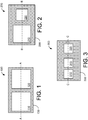
FIG. 1 is a diagram illustrating a plan view of a wafer-level semiconductor package assembly. -
FIG. 2 is a diagram illustrating a plan view of another wafer-level semiconductor package assembly. -
FIG. 3 is a diagram illustrating a plan view of yet another wafer-level semiconductor package assembly. -
FIG. 4A is a diagram illustrating cross-sectional views of a manufacturing flow for producing the wafer-level package assembly ofFIG. 1 . -
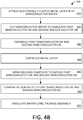
FIG. 4B is a flowchart illustrating the manufacturing flow ofFIG. 4A . -
FIG. 5A is a diagram illustrating cross-sectional views of a manufacturing flow for producing the wafer-level package assembly ofFIG. 2 . -
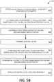
FIG. 5B is a flowchart illustrating the manufacturing flow ofFIG. 5A . -
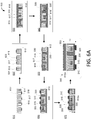
FIG. 6A is a diagram illustrating cross-sectional views of a manufacturing flow for producing the wafer-level package assembly ofFIG. 2 . -
FIG. 6B is a flowchart illustrating the manufacturing flow ofFIG. 6A . - This disclosure relates to semiconductor device package assemblies (package assemblies, packages, assemblies, etc.) and associated methods of manufacture. More specifically, this disclosure relates to multi-chip package assemblies (e.g., package assemblies that include multiple semiconductor dice) that can be produced using wafer-level processing techniques, such those described herein. While packages assemblies including two semiconductor dice are described herein, the approaches described herein can be used to produce package assemblies including different numbers of semiconductor dice, such as three semiconductor dice or more.
- The package assemblies described herein, and their associated methods of manufacture, can have certain advantages over current approaches. For instance, package assemblies described herein allow for elimination of one or more substrates in a multi-chip package assembly, and also can be produced without using wire bonding. Such approaches can allow for reduction in package assembly size, such as overall package dimensions including width, length and thickness. Alternatively, the approaches described herein can allow for the use of a larger die size in a package assembly of a given width and length. For example, current approaches can allow for semiconductor dice included in a multi-chip package assembly to have an overall surface area (e.g., combined surface area of all semiconductor dice) that is approximately 40-50% of the surface area (e.g., width x length) of the package assembly. Using the approaches described herein, the overall surface area of the semiconductor dice can be 80-90% of the package assembly surface area.
- Further, using the approaches described herein, multi-chip package assemblies having a thickness of 200 micrometers (µm) or less can be produced. Still further, manufacturing processes for producing multi-chip package assemblies as described herein may provide cost savings over current manufacturing process approaches (e.g., elimination of ceramic substrates, elimination of wire bonding processing, reduced assembly process complexity, etc.). Also, elimination of wire bonding processing can improve reliability of multi-chip package assemblies, such as those disclosed herein as compared to current multi-chip package assemblies.
-
FIG. 1 is a diagram illustrating a plan view of a wafer-levelsemiconductor package assembly 100. Thepackage assembly 100 can be produced, for example, using the assembly manufacturing flow shown inFIG. 4 , which is described below. Briefly, however, thepackage assembly 100 ofFIG. 1 is shown with a section line A-A, which is a section line along which the cross-sectional views ofFIG. 4 are taken. - As shown in
FIG. 1 , thepackage assembly 100 includes a firstelectrical contact 110 and a secondelectrical contact 120, which can both be disposed on a surface of thepackage assembly 100. In some implementations, theelectrical contact 110 can be to a first semiconductor die that is disposed within thepackage assembly 100, while theelectrical contact 120 can be to a second semiconductor die that is also disposed within thepackage assembly 100. For example, the firstelectrical contact 110 can be a surface (e.g., a portion of a surface) of the first semiconductor die, or can be a conductive material, such as a solder bump, that is disposed on a surface of the first semiconductor die. Similarly, the secondelectrical contact 120 can be a surface (e.g., a portion of a surface) of the second semiconductor die, or can be a conductive material, such as a solder bump, that is disposed on a surface of the second semiconductor die. - In some implementations, the first semiconductor die can include a first diode and the second semiconductor die can include a second diode, where the first diode is electrically coupled with the second diode within the
package assembly 100, such as using the techniques described herein. In thepackage assembly 100, the first semiconductor die and the second semiconductor die can be of a same size (e.g., approximately a same size, substantially a same size, etc.). In other implementations, the first semiconductor die and/or the second semiconductor die of thepackage assembly 200 can include different electrical devices, such as resistors, transistors, capacitors, etc. - As also shown in
FIG. 1 , thepackage assembly 100 can include amolding compound 130. Themolding compound 130 can be an epoxy molding compound, a liquid molding compound, or other appropriate molding compound for the particular implementation. The firstelectrical contact 110 and the secondelectrical contact 120 can be exposed through themolding compound 130. For example, in certain implementations, a surface of (e.g., at least a portion of a surface of) the first semiconductor die, and a surface of (e.g., at least a portion of a surface of) the second semiconductor die of thepackage assembly 100 can be exposed through themolding compound 130. Further in thepackage assembly 100, a conductive material, such as a solder or other conductive material, can be disposed on the exposed surface of the first semiconductor die and the exposed surface of second semiconductor die to form, respectively, theelectrical contact 110 and theelectrical contact 120.Electrical contacts package assembly 100 with, e.g., a printed circuit board. - As also shown in
FIG. 1 , thepackage assembly 100 can have a length of L1 and a width of W1, where L1 and W1 can vary depending on the particular implementation. In example implementations, L1 can be between 0.40 millimeters (mm) and 10.00 mm, while W1 can be between 0.20 mm and 10.00 mm. In other implementations, L1 and W1 can have different values. -
FIG. 2 is a diagram illustrating a plan view of another wafer-levelsemiconductor package assembly 200. Thepackage assembly 200 can be produced, for example, using the assembly manufacturing flow shown inFIG. 5A , which is described below. Briefly, however, thepackage assembly 200 ofFIG. 2 is shown with a section line B-B, which is a section line along which the cross-sectional views ofFIG. 5A are taken. - As shown in
FIG. 2 , thepackage assembly 200 includes a firstelectrical contact 210 and a secondelectrical contact 220, which can both be disposed on a surface of thepackage assembly 200. In some implementations, theelectrical contact 210 can be to a first semiconductor die that is disposed within thepackage assembly 200, while theelectrical contact 220 can be to a second semiconductor die that is also disposed within thepackage assembly 200. For example, the firstelectrical contact 210 can be a surface (e.g., a portion of a surface) of the first semiconductor die, or can be a conductive material, such as a solder bump, that is disposed on a surface of the first semiconductor die. Similarly, the secondelectrical contact 220 can be a surface (e.g., a portion of a surface) of the second semiconductor die, or can be a conductive material, such as a solder bump, that is disposed on a surface of the second semiconductor die. - In some implementations, the first semiconductor die can include a first diode and the second semiconductor die can include a second diode, where the first diode is electrically coupled with the second diode within the
package assembly 200, such as using the techniques described herein. In thepackage assembly 200, the first semiconductor die and the second semiconductor die can be of different sizes. For instance the first semiconductor die can be larger than the second semiconductor die (e.g., the first semiconductor die can include a diode that is larger than a diode of the second semiconductor die). In other implementations, the first semiconductor die and/or the second semiconductor die of thepackage assembly 200 can include different electrical devices, such as resistors, transistors, capacitors, etc. - As also shown in
FIG. 2 , thepackage assembly 200 can include amolding compound 230. Themolding compound 230, as with themolding compound 130 of thepackage assembly 100, can be an epoxy molding compound, a liquid molding compound, or other appropriate molding compound for the particular implementation. The firstelectrical contact 210 and the secondelectrical contact 220 can be exposed through themolding compound 230. For example, in certain implementations, a surface of (e.g., at least a portion of a surface of) the first semiconductor die, and a surface of (e.g., at least a portion of a surface of) the second semiconductor die of thepackage assembly 200 can be exposed through themolding compound 230. Further in thepackage assembly 200, a conductive material, such as a solder or other conductive material, can be disposed on the exposed surface of the first semiconductor die and the exposed surface of second semiconductor die to form, respectively, theelectrical contact 210 and theelectrical contact 220.Electrical contacts package assembly 200 with, e.g., a printed circuit board. - As also shown in
FIG. 2 , thepackage assembly 200 can have a length of L2 and a width of W2, where L2 and W2 can vary depending on the particular implementation. In example implementations, L2 can be between 0.40 mm and 10.00 mm, while W2 can be between 0.20 mm and 10.00 mm. In other implementations, L2 and W2 can have different values. -
FIG. 3 is a diagram illustrating a plan view of yet another wafer-levelsemiconductor package assembly 300. Thepackage assembly 300 can be produced, for example, using the assembly manufacturing flow shown inFIG. 6A , which is described below. Briefly, however, thepackage assembly 300 inFIG. 3 is shown with a section line C-C, which is a section line along which the cross-sectional views ofFIG. 6A are taken. - As shown in
FIG. 3 , thepackage assembly 300 includes a firstelectrical contact 310, a secondelectrical contact 315 and a thirdelectrical contact 320, which can each be disposed on a surface of thepackage assembly 300. In some implementations, theelectrical contacts package assembly 300, while theelectrical contact 320 can be to a second semiconductor die that is also disposed within thepackage assembly 300. For example, theelectrical contact 310 can be to a first signal terminal on a surface of the first semiconductor die, while theelectrical contact 315 can be to a second signal terminal on the surface of the first semiconductor die. Theelectrical contacts electrical contacts electrical contact 320 can be to the second semiconductor die. For example, theelectrical contact 320 can include a conductive pillar or post (e.g., a copper post) that is disposed on a surface of (e.g., a signal terminal) of the second semiconductor die. Theelectrical contact 320 can further include a solder bump that is formed on the conductive pillar disposed on the second semiconductor die. - In some implementations, the first semiconductor die can include a transistor device, such as a metal-oxide-semiconductor field-effect transistor (MOSFET), and the second semiconductor die can include a diode, where the transistor device is electrically coupled with the diode within the
package assembly 300, such as using the techniques described herein. For instance, a drain terminal of a MOSFET device of the first semiconductor die can be coupled with a diode of the second semiconductor die within thepackage assembly 300. In thepackage assembly 300, where the first semiconductor die includes a MOSFET device, theelectrical contact 310 can be to a source terminal of the MOSFET device, while theelectrical contact 315 is to a gate terminal of the MOSFET device, or vice versa. - In the
package assembly 300, the first semiconductor die and the second semiconductor die can be of different sizes. For instance the first semiconductor die can be larger than the second semiconductor die (e.g., the first semiconductor die can include a transistor device that is larger than a diode of the second semiconductor die). In other implementations, the first semiconductor die and/or the second semiconductor die of thepackage assembly 300 can include different electrical devices, such as resistors, transistor, capacitors, etc. - As also shown in
FIG. 3 , thepackage assembly 300 can include amolding compound 330. Themolding compound 330, as with themolding compound 130 of thepackage assembly 100 and themolding compound 230 of thepackage assembly 200, can be an epoxy molding compound, a liquid molding compound, or other appropriate molding compound for the particular implementation. The firstelectrical contact 310, the secondelectrical contact 315 and the thirdelectrical contact 320 can be exposed through themolding compound 330. For example, in certain implementations, respective conductive (e.g., copper, copper-nickel, etc.) posts for each of theelectrical contacts package assembly 300 can be exposed through themolding compound 330. Further in thepackage assembly 300, a conductive material, such as a solder bump or other conductive material, can be disposed on the exposed surfaces of the conductive posts to form, respectively, theelectrical contact 310, theelectrical contact 315, and theelectrical contact 320.Electrical contacts package assembly 300 with, e.g., a printed circuit board. - As also shown in
FIG. 3 , thepackage assembly 300 can have a length of L3 and a width of W3, where L3 and W3 can vary depending on the particular implementation. In example implementations, L3 can be between 0.40 mm and 10.00 mm, while W2 can be between 0.20 mm and 10.00 mm. In other implementations, L3 and W3 can have different values. -
FIG. 4A is a diagram including cross-sectional views that illustrate amanufacturing flow 400 for producing the wafer-level package assembly 100 ofFIG. 1 . As noted above, the wafer-level manufacturing flow 400 ofFIG. 4A is illustrated using cross-sectional views that are taken along a section line corresponding with the section line A-A shown inFIG 1 . Reference numbers fromFIG. 1 are used inFIG. 4A to reference like elements of thepackage assembly 100 ofFIG. 1 . Also inFIG. 4A , while certain reference numbers may be repeated for each of the respective cross-sectional views illustrating the various operations of themanufacturing flow 400, the elements referenced in each view may not be specifically discussed. - In the
manufacturing flow 400, atoperation 410, ametal layer 412 can be attached (disposed on) and electrically coupled with asemiconductor wafer 414. In this example, thesemiconductor wafer 414 can include the first semiconductor die (e.g., semiconductor die 422) and the second semiconductor die (e.g., semiconductor die 424) of thepackage assembly 100. As noted above with respect toFIG. 1 , in some implementations, the first semiconductor die 422 and the second semiconductor die 424 can each be diodes of a same size (e.g., substantially same size, etc.). Themetal layer 412, which can be directly disposed on the semiconductor wafer 414 (and, therefore, directly disposed on the first semiconductor die 422 and the second semiconductor die 424) can electrically couple a first side of the first semiconductor die 422 with a first side of the second semiconductor die 424, such as illustrated by the subsequent operations of themanufacturing flow 400. - In some implementations, the
metal layer 412 can be a solid metal sheet (e.g., a copper sheet, a copper-nickel sheet, etc.) that is coupled directly with the semiconductor wafer 414 (e.g., using a conductive adhesive, using solder bumps that were previously formed on thesemiconductor wafer 414, etc.). In other implementations, themetal layer 412 can be a patterned metal sheet that is coupled with (e.g., directly disposed on, etc.) thesemiconductor wafer 414. For instance, themetal layer 412 can be patterned prior to attaching (affixing, coupling, etc.) themetal layer 412 with thesemiconductor wafer 414. Alternatively, themetal layer 412 can be patterned after attaching themetal layer 412 to thesemiconductor wafer 414. In some implementations, themetal layer 412 can be a deposited metal layer that is patterned or unpatterned. - At operation 420 (for which the illustrated cross-sectional view is inverted as compared to the cross-sectional view for operation 410), the
manufacturing flow 400 includes cutting thesemiconductor wafer 414 to separate the first semiconductor die 422 from the second semiconductor die 424; to separate the first semiconductor die 422 from thesemiconductor wafer 414; and to separate the second semiconductor die 424 from thesemiconductor wafer 414. The process of separating the first semiconductor die 422 and the second semiconductor die 424 can be referred to as singulation.Operation 420 of themanufacturing flow 400 can be performed using a laser cutting process, a plasma cutting process, a mechanical sawing process, etc. The particular approach used to singulate the first semiconductor die 422 and the second semiconductor die 424 can depend on the specific implementation. - As shown in
FIG. 4A , the singulation process ofoperation 420 can also result ingrooves 426 being formed in themetal layer 412, e.g., at least between the first semiconductor die 422 and the second semiconductor die 424. For instance,grooves 426 can be formed in themetal layer 412 around a perimeter of the first semiconductor die 422 and around a perimeter of the second semiconductor die 424. - As shown in
FIG. 4A , atoperation 430, themanufacturing flow 400 includes a first molding operation to overmold the first semiconductor die 422 and the second semiconductor die 424 with themolding compound 130, such that themolding compound 130 is disposed between the first semiconductor die 422 and the second semiconductor die 424, as well as on second sides (surfaces) of the first semiconductor die 422 and the second semiconductor die 424 that are opposite the first sides of thesemiconductor dice metal layer 412 is disposed. - At operation 440 (for which the illustrated cross-sectional view is inverted as compared to the cross-sectional view for operation 430), the
manufacturing flow 400 includes a second molding operation to overmold an exposed surface of the metal layer 412 (e.g., a surface of themetal layer 412 that is opposite the surface of the metal layer that is coupled with thesemiconductor dice 422 and 424). Themolding operations manufacturing flow 400 at least partially encapsulate the first semiconductor die 422, the second semiconductor die 424 and themetal layer 412 in themolding compound 130. - At operation 450 (for which the illustrated cross-sectional view is inverted as compared to the cross-sectional view for operation 440), the
manufacturing flow 400 includes performing a grinding operation to remove a portion of themolding compound 130 from themolding operation 430, and to expose the second surface of the first semiconductor die 422 and the second surface of the second semiconductor die 424. That is, the grindingoperation 450 can be performed to expose the first semiconductor die 422 through the molding compound 130 (e.g., to facilitate formation of the firstelectrical contact 110 of the package assembly 100), and to expose the second semiconductor die 424 through the molding compound 130 (e.g., to facilitate formation of the secondelectrical contact 120 of the package assembly 100). In some implementations, the firstelectrical contact 110 can be the exposed second side of the first semiconductor die 422; and the secondelectrical contact 120 can be the exposed second side of the second semiconductor die 424. - In the
manufacturing flow 400, atoperation 460, patterned backside metal can be formed (e.g., by application of solder bumps, using photolithography, etc.) to define (form, etc.) the electrical contact 110 (on the second side of the first semiconductor die 422), and to define (form, etc.) the electrical contact 120 (on the second side of the second semiconductor die 424). Atoperation 470 of themanufacturing flow 400, another singulation process can be performed to cut themolding compound 130 and themetal layer 412 to singulate the package assembly 100 (as shown inFIG. 4A ), where the (wafer-level)package assembly 100 includes the first semiconductor die 422, the second semiconductor die 424 and aportion 412a of themetal layer 412. Thesingulation operation 470 can be performed using a laser cutting process, a plasma cutting process, a mechanical sawing process, and/or any other appropriate singulation technique. As shown inFIG. 4A , thepackage assembly 100 can have a thickness of T1, which, as noted above, can be 200 µm or less. -
FIG. 4B is a flowchart illustrating themanufacturing flow 400 ofFIG. 4A . For purposes of illustration, the same reference numbers used for the operations inFIG. 4A will be used inFIG. 4B. FIG. 4B will also be described with further reference toFIG. 1 . - At
operation 410 of themanufacturing flow 400 inFIG. 4B , themetal layer 412 can be attached (disposed on) and electrically coupled with thesemiconductor wafer 414. Atoperation 420, themanufacturing flow 400 includes cutting thesemiconductor wafer 414 to separate the first semiconductor die 422 from the second semiconductor die 424; to separate the first semiconductor die 422 from thesemiconductor wafer 414; and to separate the second semiconductor die 424 from the semiconductor wafer 414 (e.g., to singulate the first semiconductor die 422 and the second semiconductor die 424). Atoperation 430, themanufacturing flow 400 includes performing a first molding operation to overmold the first semiconductor die 422 and the second semiconductor die 424 with themolding compound 130, such as illustrated inFIG. 4A . Atoperation 440, themanufacturing flow 400 includes performing a second molding operation to overmold an exposed surface of themetal layer 412. Atoperation 450, themanufacturing flow 400 includes performing a grinding operation to remove a portion of themolding compound 130 from themolding operation 430, and to expose the second surface of the first semiconductor die 422 and the second surface of the second semiconductor die 424. Atblock 460, themanufacturing flow 400 includes forming a patterned backside metal to define (form, etc.) one or more electrical contacts, e.g., theelectrical contact 110 and theelectrical contact 120. Atoperation 470, themanufacturing flow 400 includes another singulation process can be performed to cut themolding compound 130 and themetal layer 412 to singulate the wafer-level package assembly 100. -
FIG. 5A is a diagram including cross-sectional views that illustrate amanufacturing flow 500 for producing the wafer-level package assembly 200 ofFIG. 2 . As noted above, the wafer-level manufacturing flow 500 ofFIG. 5A is illustrated using cross-sectional views that are taken along a section line corresponding with the section line B-B shown inFIG 2 . Reference numbers fromFIG. 2 are used inFIG. 5A to reference like elements of thepackage assembly 200 ofFIG. 2 . Also inFIG. 5A , while certain reference numbers may be repeated for each of the respective cross-sectional views illustrating the various operations of themanufacturing flow 500, the elements referenced in each view may not be specifically discussed. - In the
manufacturing flow 500, atoperation 510, ametal layer 512 can be attached (disposed on) and electrically coupled with asemiconductor wafer 514. In this example, thesemiconductor wafer 514 can include the first semiconductor die (e.g., semiconductor die 522) and the second semiconductor die (e.g., semiconductor die 524) of thepackage assembly 200. As noted above with respect toFIG. 2 , in some implementations, a diode of the first semiconductor die 522 can be larger than a diode of the second semiconductor die 524 (e.g., the first semiconductor die 522, accordingly, being larger than the second semiconductor die 524). Themetal layer 512, which can be directly disposed on the semiconductor wafer 514 (and, therefore, directly disposed on the first semiconductor die 522 and the second semiconductor die 524) can electrically couple a first side of the first semiconductor die 522 with a first side of the second semiconductor die 524, such as illustrated by the subsequent operations of themanufacturing flow 500. - In some implementations, the
metal layer 512 can be a solid metal sheet (e.g., a copper sheet, a copper-nickel sheet, etc.) that is coupled directly with the semiconductor wafer 514 (e.g., using a conductive adhesive, using solder bumps that were previously formed on thesemiconductor wafer 514, etc.). In other implementations, themetal layer 512 can be a patterned metal sheet that is coupled with (e.g., directly disposed on, etc.) thesemiconductor wafer 514. For instance, themetal layer 512 can be patterned prior to attaching (affixing, coupling, etc.) themetal layer 512 with thesemiconductor wafer 514. Alternatively, themetal layer 512 can be patterned after attaching themetal layer 512 to thesemiconductor wafer 514. In some implementations, themetal layer 512 can be a deposited metal layer that is patterned or unpatterned. - At operation 520 (for which the illustrated cross-sectional view is inverted as compared to the cross-sectional view for operation 510), the
manufacturing flow 500 includes cutting thesemiconductor wafer 514 to separate the first semiconductor die 522 from the second semiconductor die 524; to separate the first semiconductor die 522 from thesemiconductor wafer 514; and to separate the second semiconductor die 524 from thesemiconductor wafer 514. As withoperation 420 of themanufacturing flow 400, the process of separating the first semiconductor die 522 and the second semiconductor die 524 atoperation 520 can be referred to as singulation.Operation 520 of themanufacturing flow 500, as withoperation 420 of themanufacturing flow 400, can be performed using a laser cutting process, a plasma cutting process, a mechanical sawing process, etc. The particular approach used to singulate the first semiconductor die 522 and the second semiconductor die 524 can depend on the specific implementation. - As shown in
FIG. 5A , the singulation process ofoperation 520 can also result ingrooves 526 being formed in themetal layer 512, e.g., at least between the first semiconductor die 522 and the second semiconductor die 524. For instance,grooves 526 can be formed in themetal layer 512 around a perimeter of the first semiconductor die 522 and around a perimeter of the second semiconductor die 524. - As shown in
FIG. 5A , atoperation 530, themanufacturing flow 500 includes a first molding operation to overmold the first semiconductor die 522 and the second semiconductor die 524 with themolding compound 230, such that themolding compound 230 is disposed between the first semiconductor die 522 and the second semiconductor die 524, as well as on second sides (surfaces) of the first semiconductor die 522 and the second semiconductor die 524 that are opposite the first sides of thesemiconductor dice metal layer 512 is disposed. - At operation 540 (for which the illustrated cross-sectional view is inverted as compared to the cross-sectional view for operation 530), the
manufacturing flow 500 includes a second molding operation to overmold an exposed surface of the metal layer 512 (e.g., a surface of themetal layer 512 that is opposite the surface of the metal layer that is coupled with thesemiconductor dice 522 and 524). Themolding operations manufacturing flow 500 at least partially encapsulate the first semiconductor die 522, the second semiconductor die 524 and themetal layer 512 in themolding compound 230. - At operation 550 (for which the illustrated cross-sectional view is inverted as compared to the cross-sectional view for operation 540), the
manufacturing flow 500 includes performing a grinding operation to remove a portion of themolding compound 230 from themolding operation 530, and to expose the second surface of the first semiconductor die 522 and the second surface of the second semiconductor die 524. That is, the grindingoperation 550 can be performed to expose the first semiconductor die 522 through the molding compound 230 (e.g., to facilitate formation of the firstelectrical contact 210 of the package assembly 200), and to expose the second semiconductor die 524 through the molding compound 230 (e.g., to facilitate formation of the secondelectrical contact 220 of the package assembly 200). In some implementations, the firstelectrical contact 210 can be the exposed second side of the first semiconductor die 522; and the secondelectrical contact 220 can be the exposed second side of the second semiconductor die 524. - In the
manufacturing flow 500, atoperation 560, patterned backside metal can be formed (e.g., by application of solder bumps, using photolithography, etc.) to define (form, etc.) the electrical contact 210 (on the second side of the first semiconductor die 522), and to define (form, etc.) the electrical contact 220 (on the second side of the second semiconductor die 524). Atoperation 570 of themanufacturing flow 500, another singulation process can be performed to cut themolding compound 230 and themetal layer 512 to singulate thepackage assembly 200, where the (wafer-level)package assembly 200 includes the first semiconductor die 522, the second semiconductor die 524 and aportion 512a of themetal layer 512. Thesingulation operation 570 can be performed using a laser cutting process, a plasma cutting process, a mechanical sawing process, and/or any other appropriate singulation technique. As shown inFIG. 5A , thepackage assembly 200 can have a thickness ofT2, which, as noted above, can be 200 µm or less. -
FIG. 5B is a flowchart illustrating themanufacturing flow 500 ofFIG. 5A . For purposes of illustration, the same reference numbers used for the operations inFIG. 5A will be used inFIG. 5B. FIG. 5B will also be described with further reference toFIG. 2 . - At
operation 510 of themanufacturing flow 500 inFIG. 5B , themetal layer 512 can be attached (disposed on) and electrically coupled with thesemiconductor wafer 514. Atoperation 520, themanufacturing flow 500 includes cutting thesemiconductor wafer 514 to separate the first semiconductor die 522 from the second semiconductor die 524; to separate the first semiconductor die 522 from thesemiconductor wafer 514; and to separate the second semiconductor die 524 from the semiconductor wafer 514 (e.g., to singulate the first semiconductor die 522 and the second semiconductor die 524). Atoperation 530, themanufacturing flow 500 includes performing a first molding operation to overmold the first semiconductor die 522 and the second semiconductor die 524 with themolding compound 230, such as illustrated inFIG. 5A . Atoperation 540, themanufacturing flow 500 includes performing a second molding operation to overmold an exposed surface of themetal layer 512. Atoperation 550, themanufacturing flow 500 includes performing a grinding operation to remove a portion of themolding compound 230 from themolding operation 530, and to expose the second surface of the first semiconductor die 522 and the second surface of the second semiconductor die 524. Atblock 560, themanufacturing flow 500 includes forming a patterned backside metal to define (form, etc.) one or more electrical contacts, e.g., theelectrical contact 210 and theelectrical contact 220. Atoperation 570, themanufacturing flow 500 includes performing another singulation process to cut themolding compound 230 and themetal layer 512 to singulate the wafer-level package assembly 200. -
FIG. 6A is a diagram including cross-sectional views that illustrate amanufacturing flow 600 for producing the wafer-level package assembly 300 ofFIG. 3 . As noted above, the wafer-level manufacturing flow 600 ofFIG. 6A is illustrated using cross-sectional views that are taken along a section line corresponding with the section line C-C shown inFIG 3 . Reference numbers fromFIG. 3 are used inFIG. 6A to reference like elements of thepackage assembly 300 ofFIG. 3 . Also inFIG. 6A , while certain reference numbers may be repeated for each of the respective cross-sectional views illustrating the various operations of themanufacturing flow 600, the elements referenced in each view may not be specifically discussed. - In the
manufacturing flow 600, atoperation 610, ametal layer 612 can be attached (disposed on) and electrically coupled with a first side of asemiconductor wafer 614. In this example, thesemiconductor wafer 614 can include the first semiconductor die (e.g., semiconductor die 622) and the second semiconductor die (e.g., semiconductor die 624) of thepackage assembly 300. As noted above with respect toFIG. 3 , in this example, the first semiconductor die 622 can include a transistor (e.g., MOSFET) device, while the second semiconductor die 624 can include a diode. As also noted above with respect toFIG. 3 , in some implementations, the first semiconductor die 622 can be larger than the second semiconductor die 624, such as shown inFIG. 6A . Themetal layer 612, which can be directly disposed on the semiconductor wafer 614 (and, therefore, directly disposed on the first semiconductor die 622 and the second semiconductor die 624) can electrically couple a first side of the first semiconductor die 622 (e.g., a drain terminal of the MOSFET) with a first side (e.g., a first terminal of the diode) of the second semiconductor die 624, such as illustrated by the subsequent operations of themanufacturing flow 600. - In some implementations, the
metal layer 612 can be a solid metal sheet (e.g., a copper sheet, a copper-nickel sheet, etc.) that is coupled directly with the semiconductor wafer 614 (e.g., using a conductive adhesive, using solder bumps that were previously formed on thesemiconductor wafer 614, etc.). In other implementations, themetal layer 612 can be a patterned metal sheet that is coupled with (e.g., directly disposed on, etc.) thesemiconductor wafer 614. For instance, themetal layer 612 can be patterned prior to attaching (affixing, coupling, etc.) themetal layer 612 with thesemiconductor wafer 614. Alternatively, themetal layer 612 can be patterned after attaching themetal layer 612 to thesemiconductor wafer 614. In some implementations, themetal layer 612 can be a deposited metal layer that is patterned or unpatterned. - As also shown for
operation 610 of themanufacturing flow 600, conductive pillars (e.g., copper pillars, copper-nickel pillars, etc.) 616, 617 and 618 can be disposed on a second side of thesemiconductor wafer 614 that is opposite the side of thesemiconductor wafer 614 on which themetal layer 612 is disposed. In this example, theconductive pillar 616 can be (directly) disposed on (affixed with, coupled with, electrically coupled with, etc.) a source terminal of the MOSFET of the first semiconductor die 622. Theconductive pillar 617 can be (directly) disposed on (affixed with, coupled with, electrically coupled with, etc.) a gate terminal of the MOSFET of the first semiconductor die 622. Further in this example, theconductive pillar 618 can be (directly) disposed on (affixed with, coupled with, electrically coupled with, etc.) a second terminal of the diode of the second semiconductor die 624 (e.g., a side of the second semiconductor die 624 that is opposite to the side to which themetal layer 612 is affixed). - At operation 620 (for which the illustrated cross-sectional view is inverted as compared to the cross-sectional view for operation 610), the
manufacturing flow 600 includes cutting thesemiconductor wafer 614 to separate the first semiconductor die 622 from the second semiconductor die 624; to separate the first semiconductor die 622 from thesemiconductor wafer 614; and to separate the second semiconductor die 624 from thesemiconductor wafer 614. As withoperation 420 of themanufacturing flow 400 and theoperation 520 of themanufacturing flow 500, the process of separating the first semiconductor die 622 and the second semiconductor die 624 atoperation 620 can be referred to as singulation.Operation 620 of themanufacturing flow 600, as withoperations 420and 520 of their respective manufacturing flows 400 and 500, can be performed using a laser cutting process, a plasma cutting process, a mechanical sawing process, etc. The particular approach used to singulate the first semiconductor die 622 and the second semiconductor die 624 can depend on the specific implementation. - As shown in
FIG. 6A , the singulation process ofoperation 620 can also result in grooves 626 being formed in themetal layer 612, e.g., at least between the first semiconductor die 622 and the second semiconductor die 624. For instance, grooves 626 can be formed in themetal layer 612 around a perimeter of the first semiconductor die 622 and around a perimeter of the second semiconductor die 624. - As shown in
FIG. 6A , atoperation 630, themanufacturing flow 600 includes a first molding operation to overmold the first semiconductor die 622, the second semiconductor die 624 and theconductive pillars molding compound 330, such that themolding compound 630 is disposed between the first semiconductor die 622 and the second semiconductor die 624, as well as encapsulating the first semiconductor die 622, the second semiconductor die 624 and theconductive pillars - At operation 640 (for which the illustrated cross-sectional view is inverted as compared to the cross-sectional view for operation 630), the
manufacturing flow 600 includes a second molding operation to overmold an exposed surface of the metal layer 612 (e.g., a surface of themetal layer 612 that is opposite the surface of the metal layer that is coupled with thesemiconductor dice 622 and 624). - At operation 650 (for which the illustrated cross-sectional view is inverted as compared to the cross-sectional view for operation 640), the
manufacturing flow 600 includes performing a grinding operation to remove a portion of themolding compound 630 from themolding operation 630, and to expose theconductive pillars molding compound 330. That is, the grindingoperation 650 can be performed to expose theconductive pillars electrical contact 310, the secondelectrical contact 315 and the thirdelectrical contact 320 of thepackage assembly 300 ofFIG. 3 . - In the
manufacturing flow 600, atoperation 660, patterned backside metal can be formed (e.g., by application of solder bumps, using photolithography, etc.) to define (form, etc.) theelectrical contacts - At
operation 670 of themanufacturing flow 600, another singulation process can be performed to cut themolding compound 330 and themetal layer 612 to singulate thepackage assembly 300, where the (wafer-level)package assembly 300 includes the first semiconductor die 622, the second semiconductor die 624 and aportion 612a of themetal layer 612. Thesingulation operation 670 can be performed using a laser cutting process, a plasma cutting process, a mechanical sawing process, and/or any other appropriate singulation technique. As shown inFIG. 6A , thepackage assembly 300 can have a thickness of T3, which, as noted above, can be 200 µm or less. -
FIG. 6B is a flowchart illustrating themanufacturing flow 600 ofFIG. 6A . For purposes of illustration, the same reference numbers used for the operations inFIG. 6A will be used inFIG. 6B. FIG. 6B will also be described with further reference toFIG. 3 . - At
operation 610 of themanufacturing flow 600 inFIG. 6B , themetal layer 612 can be attached (disposed on) and electrically coupled with thesemiconductor wafer 614, and theconductive pillars semiconductor wafer 614. Atoperation 620, themanufacturing flow 600 includes cutting thesemiconductor wafer 614 to separate the first semiconductor die 622 from the second semiconductor die 624; to separate the first semiconductor die 622 from thesemiconductor wafer 614; and to separate the second semiconductor die 624 from the semiconductor wafer 614 (e.g., to singulate the first semiconductor die 622 and the second semiconductor die 624). Atoperation 630, themanufacturing flow 600 includes performing a first molding operation to overmold the first semiconductor die 622 and the second semiconductor die 624 with themolding compound 330, such as illustrated inFIG. 6A . Atoperation 640, themanufacturing flow 600 includes performing a second molding operation to overmold an exposed surface of themetal layer 612. Atoperation 650, themanufacturing flow 600 includes performing a grinding operation to remove a portion of themolding compound 330 from themolding operation 630, and to expose theconductive pillars block 660, themanufacturing flow 600 includes forming a patterned backside metal to define (form, etc.) one or more electrical contacts, e.g., theelectrical contact 310, theelectrical contact 315 and theelectrical contact 220. Atoperation 670, themanufacturing flow 600 includes performing another singulation process to cut themolding compound 330 and themetal layer 612 to singulate the wafer-level package assembly 300. - In a general aspect, an apparatus can include: a metal layer; a first semiconductor die having a first side and a second side that is opposite the first side, the first side of the first semiconductor die being disposed on the metal layer; and a second semiconductor die having a first side and a second side that is opposite the first side, the first side of the second semiconductor die being disposed on the metal layer. The metal layer can electrically couple the first side of the first semiconductor die with the first side of the second semiconductor die. The apparatus can also include a molding compound at least partially encapsulating the metal layer, the first semiconductor die and the second semiconductor die. The apparatus can further include a first electrical contact and a second electrical contact. The first electrical contact can be to the second side of the first semiconductor die, and the first electrical contact can be disposed on a surface of the apparatus. The second electrical contact can be to the second side of the second semiconductor die, and the second electrical contact can be disposed on the surface of the apparatus.
- Implementations can include one or more of the following features. For instance, the first electrical contact and the second electrical contact can be exposed through the molding compound. The first electrical contact can include at least a portion of the second side of the first semiconductor die. The second electrical contact can include at least a portion of the second side of the second semiconductor die. The first electrical contact can include a first solder bump disposed on the second side of the first semiconductor die and the second electrical contact can include a second solder bump disposed on the second side of the second semiconductor die.
- The metal layer can include a portion of a solid metal sheet. The metal layer can include a portion of a patterned metal sheet. The metal layer can include a groove disposed between the first semiconductor die and the second semiconductor die.
- The molding compound can be disposed between the first semiconductor die and the second semiconductor die.
- The first semiconductor die can include a first diode, and the second semiconductor die can include a second diode.
- The first semiconductor die can include a metal-oxide-semiconductor field-effect transistor (MOSFET); and the second semiconductor die can include a diode. The apparatus can include a third electrical contact. The third electrical contact can be to the second side of the first semiconductor die, and the third electrical contact can be disposed on the surface of the apparatus. The first electrical contact can be electrically coupled with a source terminal of the MOSFET. The third electrical contact can be electrically coupled with a gate terminal of the MOSFET. The metal layer can be electrically coupled with a drain terminal of the MOSFET.
- In another general aspect, an apparatus can include: a metal layer; a first semiconductor die having a first side and a second side that is opposite the first side, the first side of the first semiconductor die being disposed on the metal layer; and a second semiconductor die having a first side and a second side that is opposite the first side, the first side of the second semiconductor die being disposed on the metal layer. The metal layer can electrically couple the first side of the semiconductor die with the first side of the second semiconductor die. The apparatus can also include a molding compound at least partially encapsulating the metal layer, the first semiconductor die and the second semiconductor die. The apparatus can also include a first conductive pillar and a second conductive pillar. The first conductive pillar can be disposed on, and electrically coupled with the second side of the first semiconductor. The first conductive pillar can be exposed through the molding compound on a surface of the apparatus. The second conductive pillar can be disposed on, and electrically coupled with the second side of the second semiconductor die. The second conductive pillar can be exposed through the molding compound on the surface of the apparatus.
- Implementations can include one or more of the following features. For instance, the first semiconductor die can include a metal-oxide-semiconductor field-effect transistor (MOSFET) and the second semiconductor die can include a diode. The apparatus can include a third conductive pillar disposed on, and electrically coupled with the second side of the first semiconductor die. The third conductive pillar can be exposed through the molding compound on the surface of the apparatus. The first conductive pillar can be electrically coupled with a source terminal of the MOSFET. The third conductive pillar can be electrically coupled with a gate terminal of the MOSFET. The metal layer can be electrically coupled with a drain terminal of the MOSFET.
- The metal layer can include a portion of a solid metal sheet. The metal layer can include a portion of a patterned metal sheet. The metal layer can include a groove disposed between the first semiconductor die and the second semiconductor die.
- The molding compound is disposed between the first semiconductor die and the second semiconductor die.
- In another general aspect, a method can include attaching and electrically coupling a metal layer with a semiconductor wafer. The semiconductor wafer can include a first semiconductor die and a second semiconductor die. The metal layer can electrically couple a first side of the first semiconductor die with a first side of the second semiconductor die. The method can also include cutting the semiconductor wafer to: separate the first semiconductor die from the second semiconductor die; separate the first semiconductor die from the semiconductor wafer; and separate the second semiconductor die from the semiconductor wafer. The method can further include performing a molding operation to at least partially encapsulate the metal layer, the first semiconductor die and the second semiconductor die in a molding compound. The method can also further include grinding the molding compound to: expose a first electrical contact, the first electrical contact being to a second side of the first semiconductor die; and expose a second electrical contact, the second electrical contact being to a second side of the second semiconductor die. The method can still further include cutting the molding compound and the metal layer to singulate a wafer-level packaged assembly. The wafer-level packaged assembly can include the first semiconductor die and the second semiconductor die.
- Implementations can include one or more of the following features. For instance, the method can include: attaching and electrically coupling a first conductive pillar with the second side of the first semiconductor die, the first electrical contact including the first conductive pillar; and attaching and electrically coupling a second conductive pillar with the second side of the second semiconductor die, the second electrical contact including the second conductive pillar.
- In the foregoing description, when an element, such as a layer, a region, or a substrate, is referred to as being on, connected to, electrically connected to, coupled to, or electrically coupled to another element, it may be directly on, connected or coupled to the other element, or one or more intervening elements may be present. In contrast, when an element is referred to as being directly on, directly connected to or directly coupled to another element or layer, there are no intervening elements or layers present. Although the terms directly on, directly connected to, or directly coupled to may not be used throughout the detailed description, elements that are shown (e.g., in the drawings) as being directly on, directly connected or directly coupled can be referred to as such. The claims of the application may be amended to recite exemplary relationships described in the specification or shown in the figures.
- As used in this specification, a singular form may, unless definitely indicating a particular case in terms of the context, include a plural form. Spatially relative terms (e.g., over, above, upper, under, beneath, below, lower, top, bottom, and so forth) are intended to encompass different orientations of the device in use or operation in addition to the orientation depicted in the figures. In some implementations, the relative terms above and below can, respectively, include vertically above and vertically below. In some implementations, the term adjacent can include laterally adjacent to or horizontally adjacent to.
- Some implementations may be implemented using various semiconductor processing and/or packaging techniques. Some implementations may be implemented using various types of semiconductor processing techniques associated with semiconductor substrates including, but not limited to, for example, Silicon (Si), Silicon Carbide (SiC), Galium Arsenide (GaAs), Galium Nitride (GaN), and/or so forth.
- While certain features of the described implementations have been illustrated as described herein, many modifications, substitutions, changes and equivalents will now occur to those skilled in the art. The appended claims are intended to cover all such modifications and changes as fall within the scope of the implementations. The example implementations described herein and shown in the drawings have been presented by way of example only, not limitation, and various changes in form and details may be made. Any portion of the apparatus and/or methods described herein may be combined in any combination, except mutually exclusive combinations. The implementations described herein can include various combinations and/or sub-combinations of the functions, components and/or features of the different implementations described.
Claims (15)
- An apparatus comprising:a metal layer;a first semiconductor die having a first side and a second side that is opposite the first side, the first side of the first semiconductor die being disposed on the metal layer;a second semiconductor die having a first side and a second side that is opposite the first side, the first side of the second semiconductor die being disposed on the metal layer, the metal layer electrically coupling the first side of the first semiconductor die with the first side of the second semiconductor die;a molding compound at least partially encapsulating the metal layer, the first semiconductor die and the second semiconductor die;a first electrical contact, the first electrical contact being to the second side of the first semiconductor die, the first electrical contact being disposed on a surface of the apparatus; anda second electrical contact, the second electrical contact being to the second side of the second semiconductor die, the second electrical contact being disposed on the surface of the apparatus.
- The apparatus of claim 1, wherein the first electrical contact and the second electrical contact are exposed through the molding compound.
- The apparatus of any one of claims 1 or 2, wherein the first electrical contact includes at least a portion of the second side of the first semiconductor die and the second electrical contact includes at least a portion of the second side of the second semiconductor die.
- The apparatus of any one of claims 1 through 3, wherein the first electrical contact includes a first solder bump disposed on the second side of the first semiconductor die and the second electrical contact includes a second solder bump disposed on the second side of the second semiconductor die.
- The apparatus of any one of claims 1 through 4, wherein the metal layer includes a portion of a solid metal sheet.
- The apparatus of any one of claims 1 through 4, wherein the metal layer includes a portion of a patterned metal sheet.
- The apparatus of any one of claims 1 through 6, wherein the metal layer includes a groove disposed between the first semiconductor die and the second semiconductor die.
- The apparatus of any one of claims 1 through 7, wherein the molding compound is disposed between the first semiconductor die and the second semiconductor die.
- The apparatus of any one of claims 1 through 8, wherein:the first semiconductor die includes a first diode; andthe second semiconductor die includes a second diode.
- The apparatus of any one of claims 1 through 8, wherein:the first semiconductor die includes a metal-oxide-semiconductor field-effect transistor (MOSFET); andthe second semiconductor die includes a diode.
- The apparatus of claim 10, further comprising a third electrical contact, the third electrical contact being to the second side of the first semiconductor die, the third electrical contact being disposed on the surface of the apparatus,
the first electrical contact being electrically coupled with a source terminal of the MOSFET, the third electrical contact being electrically coupled with a gate terminal of the MOSFET, and the metal layer being electrically coupled with a drain terminal of the MOSFET. - The apparatus of claim 11, wherein:the first electrical contact includes a first conductive pillar disposed on, and electrically coupled with the second side of the first semiconductor die, the first conductive pillar being exposed through the molding compound on a surface of the apparatus;the second electrical contact includes a second conductive pillar disposed on, and electrically coupled with the second side of the second semiconductor die, the second conductive pillar being exposed through the molding compound on the surface of the apparatus; andthe third electrical contact includes a third conductive pillar disposed on and electrically coupled with the second side of the first semiconductor die, the third conductive pillar being exposed through the molding compound on the surface of the apparatus.
- A method comprising:attaching and electrically coupling a metal layer with a semiconductor wafer, the semiconductor wafer including a first semiconductor die and a second semiconductor die, the metal layer electrically coupling a first side of the first semiconductor die with a first side of the second semiconductor die;cutting the semiconductor wafer to:separate the first semiconductor die from the second semiconductor die;separate the first semiconductor die from the semiconductor wafer; andseparate the second semiconductor die from the semiconductor wafer;performing a molding operation to at least partially encapsulate the metal layer, the first semiconductor die and the second semiconductor die in a molding compound;grinding the molding compound to:expose a first electrical contact, the first electrical contact being to a second side of the first semiconductor die; andexpose a second electrical contact, the second electrical contact being to a second side of the second semiconductor die; andcutting the molding compound and the metal layer to singulate a wafer-level packaged assembly, the wafer-level packaged assembly including the first semiconductor die and the second semiconductor die.
- The method of claim 13, further comprising:attaching and electrically coupling a first conductive pillar with the second side of the first semiconductor die, the first electrical contact including the first conductive pillar; andattaching and electrically coupling a second conductive pillar with the second side of the second semiconductor die, the second electrical contact including the second conductive pillar.
- The method of claim 14, the grinding the molding compound further exposes a third electrical contact, the third electrical contact being to the second side of the first semiconductor die,
the first electrical contact including a first conductive pillar;
the second electrical contact including a second conductive pillar; and
the third electrical contact including a third conductive pillar.
Applications Claiming Priority (2)
| Application Number | Priority Date | Filing Date | Title |
|---|---|---|---|
| US201762549733P | 2017-08-24 | 2017-08-24 | |
| US15/812,591 US10559510B2 (en) | 2017-08-24 | 2017-11-14 | Molded wafer level packaging |
Publications (2)
| Publication Number | Publication Date |
|---|---|
| EP3447795A1 true EP3447795A1 (en) | 2019-02-27 |
| EP3447795B1 EP3447795B1 (en) | 2024-08-28 |
Family
ID=63079715
Family Applications (1)
| Application Number | Title | Priority Date | Filing Date |
|---|---|---|---|
| EP18183293.2A Active EP3447795B1 (en) | 2017-08-24 | 2018-07-13 | Molded wafer level packaging method |
Country Status (3)
| Country | Link |
|---|---|
| US (2) | US10559510B2 (en) |
| EP (1) | EP3447795B1 (en) |
| CN (1) | CN208507651U (en) |
Families Citing this family (2)
| Publication number | Priority date | Publication date | Assignee | Title |
|---|---|---|---|---|
| CN111584407B (en) * | 2020-05-29 | 2021-06-08 | 太极半导体(苏州)有限公司 | An embedded chip packaging structure and method of using the same |
| CN119092413A (en) * | 2024-11-04 | 2024-12-06 | 宁波芯健半导体有限公司 | A chip conduction connection method, system, intelligent terminal and storage medium |
Citations (6)
| Publication number | Priority date | Publication date | Assignee | Title |
|---|---|---|---|---|
| US20050023658A1 (en) * | 2003-07-31 | 2005-02-03 | Nec Electronics Corporation | Leadless type semiconductor package, and production process for manufacturing such leadless type semiconductor package |
| US20130089953A1 (en) * | 2011-10-10 | 2013-04-11 | Maxim Integrated Products, Inc. | Wafer Level Packaging Using a Lead-Frame |
| US20140091458A1 (en) * | 2012-10-01 | 2014-04-03 | Nxp B.V. | Encapsulated wafer-level chip scale (wlscp) pedestal packaging |
| EP2741327A1 (en) * | 2012-10-18 | 2014-06-11 | International Rectifier Corporation | Power converter package including top-drain configured power FET |
| US20140239413A1 (en) * | 2013-02-22 | 2014-08-28 | Stmicroelectronics S.R.L. | Power electronic device |
| US20150162270A1 (en) * | 2013-12-07 | 2015-06-11 | Fairchild Semiconductor Corporation | Packaged semiconductor devices and methods of manufacturing |
Family Cites Families (18)
| Publication number | Priority date | Publication date | Assignee | Title |
|---|---|---|---|---|
| US4754317A (en) * | 1986-04-28 | 1988-06-28 | Monolithic Memories, Inc. | Integrated circuit die-to-lead frame interconnection assembly and method |
| US6791172B2 (en) | 2001-04-25 | 2004-09-14 | General Semiconductor Of Taiwan, Ltd. | Power semiconductor device manufactured using a chip-size package |
| US6646329B2 (en) | 2001-05-15 | 2003-11-11 | Fairchild Semiconductor, Inc. | Power chip scale package |
| US6677669B2 (en) | 2002-01-18 | 2004-01-13 | International Rectifier Corporation | Semiconductor package including two semiconductor die disposed within a common clip |
| US7973398B2 (en) * | 2005-05-12 | 2011-07-05 | Unimicron Technology Corp. | Embedded chip package structure with chip support protruding section |
| US7777315B2 (en) | 2006-05-19 | 2010-08-17 | Fairchild Semiconductor Corporation | Dual side cooling integrated power device module and methods of manufacture |
| DE102007007142B4 (en) * | 2007-02-09 | 2008-11-13 | Infineon Technologies Ag | Benefits, semiconductor device and method for their production |
| SG152086A1 (en) * | 2007-10-23 | 2009-05-29 | Micron Technology Inc | Packaged semiconductor assemblies and associated systems and methods |
| US7781872B2 (en) | 2007-12-19 | 2010-08-24 | Fairchild Semiconductor Corporation | Package with multiple dies |
| WO2009122864A1 (en) * | 2008-04-01 | 2009-10-08 | シャープ株式会社 | Color filter substrate and liquid crystal display device |
| US8222078B2 (en) * | 2009-07-22 | 2012-07-17 | Alpha And Omega Semiconductor Incorporated | Chip scale surface mounted semiconductor device package and process of manufacture |
| JP2011071272A (en) * | 2009-09-25 | 2011-04-07 | Toshiba Corp | Semiconductor light-emitting device and method for manufacturing the same |
| US8987878B2 (en) * | 2010-10-29 | 2015-03-24 | Alpha And Omega Semiconductor Incorporated | Substrateless power device packages |
| JP4778107B1 (en) * | 2010-10-19 | 2011-09-21 | 有限会社ナプラ | Light emitting device and manufacturing method thereof |
| US8710648B2 (en) * | 2011-08-09 | 2014-04-29 | Alpha & Omega Semiconductor, Inc. | Wafer level packaging structure with large contact area and preparation method thereof |
| US9576887B2 (en) * | 2012-10-18 | 2017-02-21 | Infineon Technologies Americas Corp. | Semiconductor package including conductive carrier coupled power switches |
| US9087828B2 (en) * | 2013-03-12 | 2015-07-21 | Alpha & Omega Semiconductor Incorporated | Semiconductor device with thick bottom metal and preparation method thereof |
| US9673316B1 (en) * | 2013-03-15 | 2017-06-06 | Maxim Integrated Products, Inc. | Vertical semiconductor device having frontside interconnections |
-
2017
- 2017-11-14 US US15/812,591 patent/US10559510B2/en active Active
-
2018
- 2018-07-13 EP EP18183293.2A patent/EP3447795B1/en active Active
- 2018-08-14 CN CN201821307619.7U patent/CN208507651U/en active Active
-
2019
- 2019-12-20 US US16/722,376 patent/US10916485B2/en active Active
Patent Citations (6)
| Publication number | Priority date | Publication date | Assignee | Title |
|---|---|---|---|---|
| US20050023658A1 (en) * | 2003-07-31 | 2005-02-03 | Nec Electronics Corporation | Leadless type semiconductor package, and production process for manufacturing such leadless type semiconductor package |
| US20130089953A1 (en) * | 2011-10-10 | 2013-04-11 | Maxim Integrated Products, Inc. | Wafer Level Packaging Using a Lead-Frame |
| US20140091458A1 (en) * | 2012-10-01 | 2014-04-03 | Nxp B.V. | Encapsulated wafer-level chip scale (wlscp) pedestal packaging |
| EP2741327A1 (en) * | 2012-10-18 | 2014-06-11 | International Rectifier Corporation | Power converter package including top-drain configured power FET |
| US20140239413A1 (en) * | 2013-02-22 | 2014-08-28 | Stmicroelectronics S.R.L. | Power electronic device |
| US20150162270A1 (en) * | 2013-12-07 | 2015-06-11 | Fairchild Semiconductor Corporation | Packaged semiconductor devices and methods of manufacturing |
Also Published As
| Publication number | Publication date |
|---|---|
| US10916485B2 (en) | 2021-02-09 |
| CN208507651U (en) | 2019-02-15 |
| US10559510B2 (en) | 2020-02-11 |
| EP3447795B1 (en) | 2024-08-28 |
| US20200126880A1 (en) | 2020-04-23 |
| US20190067143A1 (en) | 2019-02-28 |
Similar Documents
| Publication | Publication Date | Title |
|---|---|---|
| US6316287B1 (en) | Chip scale surface mount packages for semiconductor device and process of fabricating the same | |
| US9054063B2 (en) | High power single-die semiconductor package | |
| US10410941B2 (en) | Wafer level semiconductor device with wettable flanks | |
| US9478484B2 (en) | Semiconductor packages and methods of formation thereof | |
| EP1085570A2 (en) | Chip scale surface mount package for semiconductor device and process of fabricating the same | |
| US7224045B2 (en) | Leadless type semiconductor package, and production process for manufacturing such leadless type semiconductor package | |
| JP4547279B2 (en) | Manufacturing method of semiconductor device | |
| CN101465301A (en) | Wafer level chip scale packaging | |
| US20030025183A1 (en) | Packaged semiconductor device and method of manufacture using shaped die | |
| US20250157857A1 (en) | Component and method of manufacturing a component using an ultrathin carrier | |
| EP3306660A2 (en) | Leadframe-less surface mount semiconductor device | |
| US9806056B2 (en) | Method of packaging integrated circuits | |
| US11721654B2 (en) | Ultra-thin multichip power devices | |
| US10916485B2 (en) | Molded wafer level packaging | |
| US8981566B2 (en) | Discrete semiconductor device package and manufacturing method | |
| CN103545283B (en) | Semiconductor packages with multiple lead frames and forming method thereof | |
| CN103779303A (en) | Bump package and methods of formation thereof | |
| KR20080026221A (en) | Semiconductor device manufacturing method, device chip packaging method, semiconductor device and array | |
| US9685398B2 (en) | Thin semiconductor device packages | |
| US9947551B2 (en) | Chip package structure and manufacturing method thereof | |
| EP3754691A1 (en) | Semiconductor package having a laser-activatable mold compound | |
| US20230170282A1 (en) | Non-coplanar or bumped lead frame for electronic isolation device |
Legal Events
| Date | Code | Title | Description |
|---|---|---|---|
| PUAI | Public reference made under article 153(3) epc to a published international application that has entered the european phase |
Free format text: ORIGINAL CODE: 0009012 |
|
| STAA | Information on the status of an ep patent application or granted ep patent |
Free format text: STATUS: THE APPLICATION HAS BEEN PUBLISHED |
|
| AK | Designated contracting states |
Kind code of ref document: A1 Designated state(s): AL AT BE BG CH CY CZ DE DK EE ES FI FR GB GR HR HU IE IS IT LI LT LU LV MC MK MT NL NO PL PT RO RS SE SI SK SM TR |
|
| AX | Request for extension of the european patent |
Extension state: BA ME |
|
| STAA | Information on the status of an ep patent application or granted ep patent |
Free format text: STATUS: REQUEST FOR EXAMINATION WAS MADE |
|
| 17P | Request for examination filed |
Effective date: 20190826 |
|
| RBV | Designated contracting states (corrected) |
Designated state(s): AL AT BE BG CH CY CZ DE DK EE ES FI FR GB GR HR HU IE IS IT LI LT LU LV MC MK MT NL NO PL PT RO RS SE SI SK SM TR |
|
| STAA | Information on the status of an ep patent application or granted ep patent |
Free format text: STATUS: EXAMINATION IS IN PROGRESS |
|
| 17Q | First examination report despatched |
Effective date: 20211122 |
|
| P01 | Opt-out of the competence of the unified patent court (upc) registered |
Effective date: 20230525 |
|
| GRAP | Despatch of communication of intention to grant a patent |
Free format text: ORIGINAL CODE: EPIDOSNIGR1 |
|
| STAA | Information on the status of an ep patent application or granted ep patent |
Free format text: STATUS: GRANT OF PATENT IS INTENDED |
|
| RIC1 | Information provided on ipc code assigned before grant |
Ipc: H01L 21/60 20060101ALI20240212BHEP Ipc: H01L 21/78 20060101ALI20240212BHEP Ipc: H01L 21/56 20060101ALI20240212BHEP Ipc: H01L 23/495 20060101ALI20240212BHEP Ipc: H01L 23/31 20060101AFI20240212BHEP |
|
| INTG | Intention to grant announced |
Effective date: 20240227 |
|
| GRAS | Grant fee paid |
Free format text: ORIGINAL CODE: EPIDOSNIGR3 |
|
| GRAA | (expected) grant |
Free format text: ORIGINAL CODE: 0009210 |
|
| STAA | Information on the status of an ep patent application or granted ep patent |
Free format text: STATUS: THE PATENT HAS BEEN GRANTED |
|
| AK | Designated contracting states |
Kind code of ref document: B1 Designated state(s): AL AT BE BG CH CY CZ DE DK EE ES FI FR GB GR HR HU IE IS IT LI LT LU LV MC MK MT NL NO PL PT RO RS SE SI SK SM TR |
|
| REG | Reference to a national code |
Ref country code: GB Ref legal event code: FG4D |
|
| REG | Reference to a national code |
Ref country code: CH Ref legal event code: EP |
|
| REG | Reference to a national code |
Ref country code: DE Ref legal event code: R096 Ref document number: 602018073559 Country of ref document: DE |
|
| REG | Reference to a national code |
Ref country code: IE Ref legal event code: FG4D |
|
| REG | Reference to a national code |
Ref country code: LT Ref legal event code: MG9D |
|
| PG25 | Lapsed in a contracting state [announced via postgrant information from national office to epo] |
Ref country code: NO Free format text: LAPSE BECAUSE OF FAILURE TO SUBMIT A TRANSLATION OF THE DESCRIPTION OR TO PAY THE FEE WITHIN THE PRESCRIBED TIME-LIMIT Effective date: 20241128 |
|
| REG | Reference to a national code |
Ref country code: AT Ref legal event code: MK05 Ref document number: 1718963 Country of ref document: AT Kind code of ref document: T Effective date: 20240828 |
|
| PG25 | Lapsed in a contracting state [announced via postgrant information from national office to epo] |
Ref country code: NL Free format text: LAPSE BECAUSE OF FAILURE TO SUBMIT A TRANSLATION OF THE DESCRIPTION OR TO PAY THE FEE WITHIN THE PRESCRIBED TIME-LIMIT Effective date: 20240828 Ref country code: PT Free format text: LAPSE BECAUSE OF FAILURE TO SUBMIT A TRANSLATION OF THE DESCRIPTION OR TO PAY THE FEE WITHIN THE PRESCRIBED TIME-LIMIT Effective date: 20241230 Ref country code: FI Free format text: LAPSE BECAUSE OF FAILURE TO SUBMIT A TRANSLATION OF THE DESCRIPTION OR TO PAY THE FEE WITHIN THE PRESCRIBED TIME-LIMIT Effective date: 20240828 Ref country code: GR Free format text: LAPSE BECAUSE OF FAILURE TO SUBMIT A TRANSLATION OF THE DESCRIPTION OR TO PAY THE FEE WITHIN THE PRESCRIBED TIME-LIMIT Effective date: 20241129 Ref country code: PL Free format text: LAPSE BECAUSE OF FAILURE TO SUBMIT A TRANSLATION OF THE DESCRIPTION OR TO PAY THE FEE WITHIN THE PRESCRIBED TIME-LIMIT Effective date: 20240828 |
|
| PG25 | Lapsed in a contracting state [announced via postgrant information from national office to epo] |
Ref country code: BG Free format text: LAPSE BECAUSE OF FAILURE TO SUBMIT A TRANSLATION OF THE DESCRIPTION OR TO PAY THE FEE WITHIN THE PRESCRIBED TIME-LIMIT Effective date: 20240828 |
|
| PG25 | Lapsed in a contracting state [announced via postgrant information from national office to epo] |
Ref country code: LV Free format text: LAPSE BECAUSE OF FAILURE TO SUBMIT A TRANSLATION OF THE DESCRIPTION OR TO PAY THE FEE WITHIN THE PRESCRIBED TIME-LIMIT Effective date: 20240828 |
|
| REG | Reference to a national code |
Ref country code: NL Ref legal event code: MP Effective date: 20240828 |
|
| PG25 | Lapsed in a contracting state [announced via postgrant information from national office to epo] |
Ref country code: AT Free format text: LAPSE BECAUSE OF FAILURE TO SUBMIT A TRANSLATION OF THE DESCRIPTION OR TO PAY THE FEE WITHIN THE PRESCRIBED TIME-LIMIT Effective date: 20240828 Ref country code: IS Free format text: LAPSE BECAUSE OF FAILURE TO SUBMIT A TRANSLATION OF THE DESCRIPTION OR TO PAY THE FEE WITHIN THE PRESCRIBED TIME-LIMIT Effective date: 20241228 |
|
| PG25 | Lapsed in a contracting state [announced via postgrant information from national office to epo] |
Ref country code: HR Free format text: LAPSE BECAUSE OF FAILURE TO SUBMIT A TRANSLATION OF THE DESCRIPTION OR TO PAY THE FEE WITHIN THE PRESCRIBED TIME-LIMIT Effective date: 20240828 |
|
| PG25 | Lapsed in a contracting state [announced via postgrant information from national office to epo] |
Ref country code: ES Free format text: LAPSE BECAUSE OF FAILURE TO SUBMIT A TRANSLATION OF THE DESCRIPTION OR TO PAY THE FEE WITHIN THE PRESCRIBED TIME-LIMIT Effective date: 20240828 Ref country code: RS Free format text: LAPSE BECAUSE OF FAILURE TO SUBMIT A TRANSLATION OF THE DESCRIPTION OR TO PAY THE FEE WITHIN THE PRESCRIBED TIME-LIMIT Effective date: 20241128 |
|
| PG25 | Lapsed in a contracting state [announced via postgrant information from national office to epo] |
Ref country code: RS Free format text: LAPSE BECAUSE OF FAILURE TO SUBMIT A TRANSLATION OF THE DESCRIPTION OR TO PAY THE FEE WITHIN THE PRESCRIBED TIME-LIMIT Effective date: 20241128 Ref country code: PT Free format text: LAPSE BECAUSE OF FAILURE TO SUBMIT A TRANSLATION OF THE DESCRIPTION OR TO PAY THE FEE WITHIN THE PRESCRIBED TIME-LIMIT Effective date: 20241230 Ref country code: PL Free format text: LAPSE BECAUSE OF FAILURE TO SUBMIT A TRANSLATION OF THE DESCRIPTION OR TO PAY THE FEE WITHIN THE PRESCRIBED TIME-LIMIT Effective date: 20240828 Ref country code: NO Free format text: LAPSE BECAUSE OF FAILURE TO SUBMIT A TRANSLATION OF THE DESCRIPTION OR TO PAY THE FEE WITHIN THE PRESCRIBED TIME-LIMIT Effective date: 20241128 Ref country code: NL Free format text: LAPSE BECAUSE OF FAILURE TO SUBMIT A TRANSLATION OF THE DESCRIPTION OR TO PAY THE FEE WITHIN THE PRESCRIBED TIME-LIMIT Effective date: 20240828 Ref country code: LV Free format text: LAPSE BECAUSE OF FAILURE TO SUBMIT A TRANSLATION OF THE DESCRIPTION OR TO PAY THE FEE WITHIN THE PRESCRIBED TIME-LIMIT Effective date: 20240828 Ref country code: IS Free format text: LAPSE BECAUSE OF FAILURE TO SUBMIT A TRANSLATION OF THE DESCRIPTION OR TO PAY THE FEE WITHIN THE PRESCRIBED TIME-LIMIT Effective date: 20241228 Ref country code: HR Free format text: LAPSE BECAUSE OF FAILURE TO SUBMIT A TRANSLATION OF THE DESCRIPTION OR TO PAY THE FEE WITHIN THE PRESCRIBED TIME-LIMIT Effective date: 20240828 Ref country code: GR Free format text: LAPSE BECAUSE OF FAILURE TO SUBMIT A TRANSLATION OF THE DESCRIPTION OR TO PAY THE FEE WITHIN THE PRESCRIBED TIME-LIMIT Effective date: 20241129 Ref country code: FI Free format text: LAPSE BECAUSE OF FAILURE TO SUBMIT A TRANSLATION OF THE DESCRIPTION OR TO PAY THE FEE WITHIN THE PRESCRIBED TIME-LIMIT Effective date: 20240828 Ref country code: ES Free format text: LAPSE BECAUSE OF FAILURE TO SUBMIT A TRANSLATION OF THE DESCRIPTION OR TO PAY THE FEE WITHIN THE PRESCRIBED TIME-LIMIT Effective date: 20240828 Ref country code: BG Free format text: LAPSE BECAUSE OF FAILURE TO SUBMIT A TRANSLATION OF THE DESCRIPTION OR TO PAY THE FEE WITHIN THE PRESCRIBED TIME-LIMIT Effective date: 20240828 Ref country code: AT Free format text: LAPSE BECAUSE OF FAILURE TO SUBMIT A TRANSLATION OF THE DESCRIPTION OR TO PAY THE FEE WITHIN THE PRESCRIBED TIME-LIMIT Effective date: 20240828 |
|
| PG25 | Lapsed in a contracting state [announced via postgrant information from national office to epo] |
Ref country code: DK Free format text: LAPSE BECAUSE OF FAILURE TO SUBMIT A TRANSLATION OF THE DESCRIPTION OR TO PAY THE FEE WITHIN THE PRESCRIBED TIME-LIMIT Effective date: 20240828 Ref country code: RO Free format text: LAPSE BECAUSE OF FAILURE TO SUBMIT A TRANSLATION OF THE DESCRIPTION OR TO PAY THE FEE WITHIN THE PRESCRIBED TIME-LIMIT Effective date: 20240828 Ref country code: SM Free format text: LAPSE BECAUSE OF FAILURE TO SUBMIT A TRANSLATION OF THE DESCRIPTION OR TO PAY THE FEE WITHIN THE PRESCRIBED TIME-LIMIT Effective date: 20240828 |
|
| PG25 | Lapsed in a contracting state [announced via postgrant information from national office to epo] |
Ref country code: EE Free format text: LAPSE BECAUSE OF FAILURE TO SUBMIT A TRANSLATION OF THE DESCRIPTION OR TO PAY THE FEE WITHIN THE PRESCRIBED TIME-LIMIT Effective date: 20240828 |
|
| PG25 | Lapsed in a contracting state [announced via postgrant information from national office to epo] |
Ref country code: CZ Free format text: LAPSE BECAUSE OF FAILURE TO SUBMIT A TRANSLATION OF THE DESCRIPTION OR TO PAY THE FEE WITHIN THE PRESCRIBED TIME-LIMIT Effective date: 20240828 |
|
| PG25 | Lapsed in a contracting state [announced via postgrant information from national office to epo] |
Ref country code: IT Free format text: LAPSE BECAUSE OF FAILURE TO SUBMIT A TRANSLATION OF THE DESCRIPTION OR TO PAY THE FEE WITHIN THE PRESCRIBED TIME-LIMIT Effective date: 20240828 Ref country code: SK Free format text: LAPSE BECAUSE OF FAILURE TO SUBMIT A TRANSLATION OF THE DESCRIPTION OR TO PAY THE FEE WITHIN THE PRESCRIBED TIME-LIMIT Effective date: 20240828 |
|
| REG | Reference to a national code |
Ref country code: DE Ref legal event code: R097 Ref document number: 602018073559 Country of ref document: DE |
|
| PLBE | No opposition filed within time limit |
Free format text: ORIGINAL CODE: 0009261 |
|
| STAA | Information on the status of an ep patent application or granted ep patent |
Free format text: STATUS: NO OPPOSITION FILED WITHIN TIME LIMIT |
|
| PGFP | Annual fee paid to national office [announced via postgrant information from national office to epo] |
Ref country code: GB Payment date: 20250619 Year of fee payment: 8 |
|
| 26N | No opposition filed |
Effective date: 20250530 |
|
| PG25 | Lapsed in a contracting state [announced via postgrant information from national office to epo] |
Ref country code: SE Free format text: LAPSE BECAUSE OF FAILURE TO SUBMIT A TRANSLATION OF THE DESCRIPTION OR TO PAY THE FEE WITHIN THE PRESCRIBED TIME-LIMIT Effective date: 20240828 |
|
| PGFP | Annual fee paid to national office [announced via postgrant information from national office to epo] |
Ref country code: DE Payment date: 20250620 Year of fee payment: 8 |
|
| REG | Reference to a national code |
Ref country code: DE Ref legal event code: R079 Ref document number: 602018073559 Country of ref document: DE Free format text: PREVIOUS MAIN CLASS: H01L0023310000 Ipc: H10W0074100000 |
|
| REG | Reference to a national code |
Ref country code: CH Ref legal event code: H13 Free format text: ST27 STATUS EVENT CODE: U-0-0-H10-H13 (AS PROVIDED BY THE NATIONAL OFFICE) Effective date: 20260224 |
|
| PG25 | Lapsed in a contracting state [announced via postgrant information from national office to epo] |
Ref country code: LU Free format text: LAPSE BECAUSE OF NON-PAYMENT OF DUE FEES Effective date: 20250713 |
|
| REG | Reference to a national code |
Ref country code: BE Ref legal event code: MM Effective date: 20250731 |
|
| PG25 | Lapsed in a contracting state [announced via postgrant information from national office to epo] |
Ref country code: BE Free format text: LAPSE BECAUSE OF NON-PAYMENT OF DUE FEES Effective date: 20250731 |
|
| PG25 | Lapsed in a contracting state [announced via postgrant information from national office to epo] |
Ref country code: FR Free format text: LAPSE BECAUSE OF NON-PAYMENT OF DUE FEES Effective date: 20250731 |
|
| PG25 | Lapsed in a contracting state [announced via postgrant information from national office to epo] |
Ref country code: CH Free format text: LAPSE BECAUSE OF NON-PAYMENT OF DUE FEES Effective date: 20250731 |