EP3447562A1 - Pixel elements including light emitters of variable heights - Google Patents
Pixel elements including light emitters of variable heights Download PDFInfo
- Publication number
- EP3447562A1 EP3447562A1 EP18189101.1A EP18189101A EP3447562A1 EP 3447562 A1 EP3447562 A1 EP 3447562A1 EP 18189101 A EP18189101 A EP 18189101A EP 3447562 A1 EP3447562 A1 EP 3447562A1
- Authority
- EP
- European Patent Office
- Prior art keywords
- pixel
- sub
- height
- substrate
- microbumps
- Prior art date
- Legal status (The legal status is an assumption and is not a legal conclusion. Google has not performed a legal analysis and makes no representation as to the accuracy of the status listed.)
- Granted
Links
Images




Classifications
-
- G—PHYSICS
- G02—OPTICS
- G02B—OPTICAL ELEMENTS, SYSTEMS OR APPARATUS
- G02B27/00—Optical systems or apparatus not provided for by any of the groups G02B1/00 - G02B26/00, G02B30/00
- G02B27/01—Head-up displays
- G02B27/017—Head mounted
- G02B27/0172—Head mounted characterised by optical features
-
- H—ELECTRICITY
- H10—SEMICONDUCTOR DEVICES; ELECTRIC SOLID-STATE DEVICES NOT OTHERWISE PROVIDED FOR
- H10W—GENERIC PACKAGES, INTERCONNECTIONS, CONNECTORS OR OTHER CONSTRUCTIONAL DETAILS OF DEVICES COVERED BY CLASS H10
- H10W90/00—Package configurations
-
- G—PHYSICS
- G02—OPTICS
- G02B—OPTICAL ELEMENTS, SYSTEMS OR APPARATUS
- G02B27/00—Optical systems or apparatus not provided for by any of the groups G02B1/00 - G02B26/00, G02B30/00
- G02B27/0025—Optical systems or apparatus not provided for by any of the groups G02B1/00 - G02B26/00, G02B30/00 for optical correction, e.g. distorsion, aberration
-
- G—PHYSICS
- G02—OPTICS
- G02B—OPTICAL ELEMENTS, SYSTEMS OR APPARATUS
- G02B27/00—Optical systems or apparatus not provided for by any of the groups G02B1/00 - G02B26/00, G02B30/00
- G02B27/01—Head-up displays
- G02B27/017—Head mounted
-
- G—PHYSICS
- G06—COMPUTING OR CALCULATING; COUNTING
- G06F—ELECTRIC DIGITAL DATA PROCESSING
- G06F1/00—Details not covered by groups G06F3/00 - G06F13/00 and G06F21/00
- G06F1/16—Constructional details or arrangements
- G06F1/1613—Constructional details or arrangements for portable computers
- G06F1/163—Wearable computers, e.g. on a belt
-
- H—ELECTRICITY
- H04—ELECTRIC COMMUNICATION TECHNIQUE
- H04N—PICTORIAL COMMUNICATION, e.g. TELEVISION
- H04N13/00—Stereoscopic video systems; Multi-view video systems; Details thereof
- H04N13/30—Image reproducers
- H04N13/332—Displays for viewing with the aid of special glasses or head-mounted displays [HMD]
- H04N13/344—Displays for viewing with the aid of special glasses or head-mounted displays [HMD] with head-mounted left-right displays
-
- G—PHYSICS
- G02—OPTICS
- G02B—OPTICAL ELEMENTS, SYSTEMS OR APPARATUS
- G02B27/00—Optical systems or apparatus not provided for by any of the groups G02B1/00 - G02B26/00, G02B30/00
- G02B27/01—Head-up displays
- G02B27/0101—Head-up displays characterised by optical features
- G02B2027/0112—Head-up displays characterised by optical features comprising device for genereting colour display
- G02B2027/0116—Head-up displays characterised by optical features comprising device for genereting colour display comprising devices for correcting chromatic aberration
-
- G—PHYSICS
- G02—OPTICS
- G02B—OPTICAL ELEMENTS, SYSTEMS OR APPARATUS
- G02B27/00—Optical systems or apparatus not provided for by any of the groups G02B1/00 - G02B26/00, G02B30/00
- G02B27/01—Head-up displays
- G02B27/017—Head mounted
- G02B2027/0178—Eyeglass type
-
- G—PHYSICS
- G02—OPTICS
- G02B—OPTICAL ELEMENTS, SYSTEMS OR APPARATUS
- G02B3/00—Simple or compound lenses
- G02B3/02—Simple or compound lenses with non-spherical faces
Definitions
- the second sub-pixel 420 is a light emitting element that emits a light of a second optical band.
- the second sub-pixel 420 is mounted on the substrate 210 by the microbump 230.
- the third sub-pixel 430 is similar to the second sub-pixel 260 of FIG. 2 except for the presence of a template layer 425.
- the portion of the optical block 505 directs the blue light 525 and the blue light 530 with a significant divergence such that the user's eye 150 would see a viewable media corresponding to the blue light 525 and the blue light 530 at a virtual image plane 540.
- the difference in relative positions of the virtual image plane 535 and the virtual image plane 540 with reference to the optical axis 510 results in a longitudinal chromatic aberration when presented to the user's eye 150.
- Embodiments of the disclosure may also relate to a product that is produced by a computing process described herein.
- a product may comprise information resulting from a computing process, where the information is stored on a non-transitory, tangible computer readable storage medium and may include any embodiment of a computer program product or other data combination described herein.
- the language used in the specification has been principally selected for readability and instructional purposes, and it may not have been selected to delineate or circumscribe the inventive subject matter. It is therefore intended that the scope of the disclosure be limited not by this detailed description, but rather by any claims that issue on an application based hereon. Accordingly, the disclosure of the embodiments is intended to be illustrative, but not limiting, of the scope of the disclosure, which is set forth in the following claims.
Landscapes
- Physics & Mathematics (AREA)
- General Physics & Mathematics (AREA)
- Engineering & Computer Science (AREA)
- Optics & Photonics (AREA)
- Computer Hardware Design (AREA)
- Theoretical Computer Science (AREA)
- Human Computer Interaction (AREA)
- General Engineering & Computer Science (AREA)
- Multimedia (AREA)
- Signal Processing (AREA)
- Devices For Indicating Variable Information By Combining Individual Elements (AREA)
- Led Device Packages (AREA)
Abstract
Description
- The disclosure relates generally to head-mounted-display (HMD) systems, and more specifically to manufacturing micropixels of variable height in an electronic display of the HMD system.
- A head-mounted display (HMD) presents a viewable media to a user. Conventional HMDs generally have a display element that generates image light that passes through an optical system before reaching the user's eyes. In conventional optical systems, each of the pixels are on a same planar surface of the display element. Such planar configurations of pixels in conventional HMDs often result in optical distortion (e.g. chromatic aberration, field curvature) in content presented to the user.
- A head-mounted display (HMD) presents a viewable media to a user. The HMD includes a light source and an optical block. The light source includes a first sub-pixel, and a second sub-pixel. The first sub-pixel is mounted on a first set of microbumps at a first height and the first sub-pixel emits light within a first optical band. The second sub-pixel is mounted on a second set of microbumps at a second height, and the second sub-pixel emits light over a second optical band that is different from the first optical band. The optical block receives the image light from the light source, and directs the image light to an eyebox. The first height and the second height are configured to mitigate longitudinal chromatic aberration in the optical block. The light source also corrects the field curvature of the optical block based on varying the first height and the second height. In some configurations, the light source includes a third sub-pixel mounted on a third set of microbumps at a third height from the substrate different from the second height, and the third sub-pixel emits light over a third optical band that is different than the first optical band and the second optical band. In some embodiments, each of the first sub-pixel, the second sub-pixel, and the third sub-pixel comprises a plurality of light emitting elements.
- In some embodiments, the substrate can be micromachined to vary the thickness of the substrate to mitigate longitudinal chromatic aberration in the optical block. In alternate embodiments, the substrate may be deposited with one or more additive layers to achieve a threshold value of thickness of the substrate to mitigate longitudinal chromatic aberration in the optical block. In a different embodiment, the first sub-pixel includes a template layer that compensates the stress from the substrate.
- Embodiments according to the invention are in particular disclosed in the attached claims directed to a head-mounted display (HMD) and an electronic display, wherein any feature mentioned in one claim category, e.g. HMD, can be claimed in another claim category, e.g. display, system, storage medium, computer program product, and method, as well. The dependencies or references back in the attached claims are chosen for formal reasons only. However any subject matter resulting from a deliberate reference back to any previous claims (in particular multiple dependencies) can be claimed as well, so that any combination of claims and the features thereof is disclosed and can be claimed regardless of the dependencies chosen in the attached claims. The subject-matter which can be claimed comprises not only the combinations of features as set out in the attached claims but also any other combination of features in the claims, wherein each feature mentioned in the claims can be combined with any other feature or combination of other features in the claims. Furthermore, any of the embodiments and features described or depicted herein can be claimed in a separate claim and/or in any combination with any embodiment or feature described or depicted herein or with any of the features of the attached claims.
- In an embodiment according to the invention, a head-mounted display may comprise:
- a light source comprising a plurality of pixel elements configured to emit image light that includes at least two different optical bands of light, the light source further comprising:
- a first sub-pixel mounted on a first set of microbumps at a first height from a substrate and configured to emit light within a first optical band, and
- a second sub-pixel mounted on a second set of microbumps at a second height from the substrate that is different from the first height, and the second sub-pixel is configured to emit light over a second optical band that is different than the first optical band, each of the first sub-pixel and the second sub-pixel comprising a plurality of light emitting elements; and
- an optical block configured to receive the image light from the light source, and direct the image light to an eyebox, wherein the first height and the second height are configured to mitigate longitudinal chromatic aberration in the optical block.
- The light source may include a third sub-pixel mounted on a third set of microbumps at a third height from the substrate different from the second height, and the third sub-pixel may be configured to emit light over a third optical band that is different than the first optical band and the second optical band, the third sub-pixel may comprise a plurality of light emitting elements.
- The substrate may be micromachined to a threshold value of thickness at one or more locations on the substrate to mount the third sub-pixel, the threshold value of thickness may be determined based on the first height and the second height to mitigate longitudinal chromatic aberration in the optical block.
- The threshold value of thickness may be achieved by depositing one or more additive layers on the substrate to form one or more standoff portions, each standoff portion mounting at least the first sub-pixel and the second sub-pixel at a fourth height different from the third height to mitigate longitudinal chromatic aberration in the optical block.
- The light source may include a template layer in each of the first sub-pixel and the second sub-pixel, the template layer may be configured to compensate a stress due to lattice mismatch with the substrate.
- The third height from the substrate may be different from the first height.
- The first set of microbumps and the second set of microbumps may be associated with one or more out-of-plane heights determined based on a distance of separation from the optical block, the difference between the out-of-plane height and the distance of separation may be compensating for a field curvature of the optical block.
- The first set of microbumps and the second set of microbumps may be mounted on the substrate micromachined to a threshold value of thickness to mitigate longitudinal chromatic aberration in the optical block.
- The first set of microbumps may mount the first sub-pixel including a first template layer and the second set of microbumps may mount a second sub-pixel including a second template layer different from the first template layer to mitigate longitudinal chromatic aberration in the optical block.
- In an embodiment according to the invention, an electronic display may comprise:
- a substrate;
- a plurality of microbumps;
- a first sub-pixel mounted on a first set of microbumps on the substrate at a first height and configured to emit light within a first optical band; and
- a second sub-pixel mounted on a second set of microbumps on the substrate at a second height that is different from the first height, and the second sub-pixel is configured to emit light within a second optical band that is different than the first optical band, wherein the first height and the second height are configured to mitigate longitudinal chromatic aberration in an optical block receiving light from the electronic display, each of the first sub-pixel and the second sub-pixel comprising a plurality of light emitting elements.
- In an embodiment according to the invention, an electronic display may comprise:
a third sub-pixel mounted on a third set of microbumps at a third height different from the second height, and the third sub-pixel is configured to emit light over a third optical band that is different than the first optical band and the second optical band, the third sub-pixel comprising a plurality of light emitting elements. - The substrate may be micromachined to a threshold value of thickness at one or more locations on the substrate to mount the third sub-pixel, the threshold value of thickness may be determined based on the first height and the second height to mitigate longitudinal chromatic aberration in the optical block.
- The threshold value of thickness may be achieved by depositing one or more additive layers on the substrate to form one or more standoff portions, each standoff portion may be mounting at least the first sub-pixel and the second sub-pixel at a fourth height different from the third height.
- The third height from the substrate may be different from the first height.
- The light source may include a template layer in each of the first sub-pixel and the second sub-pixel, the template layer may be configured to compensate a stress due to lattice mismatch with the substrate.
- The first set of microbumps and the second set of microbumps may be associated with one or more out-of-plane heights determined based on a distance of separation from the optical block, the difference between the out-of-plane height and the distance of separation may be compensating for a field curvature of the optical block.
- The first set of microbumps and the second set of microbumps may be mounted on the substrate micromachined to a threshold value of thickness to mitigate longitudinal chromatic aberration in the optical block.
- The first set of microbumps may mount the first sub-pixel including a first template layer and the second set of microbumps may mount a second sub-pixel including a second template layer different from the first template layer to mitigate longitudinal chromatic aberration in the optical block.
- In a further embodiment of the invention, one or more computer-readable non-transitory storage media embody software that is operable when executed to perform in a system according to the invention or any of the above mentioned embodiments.
- In a further embodiment of the invention, a computer program product, preferably comprising a computer-readable non-transitory storage media, is used in a system according to the invention or any of the above mentioned embodiments.
- In a further embodiment of the invention, a computer-implemented method uses a system according to the invention or any of the above mentioned embodiments.
-
- FIG. 1A
- is a diagram of a HMD, in accordance with at least one embodiment.
- FIG. 1B
- is a cross section of a front rigid body of the HMD in
FIG. 1A , in accordance with an embodiment. - FIG. 2
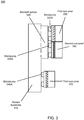
- is a pixel element including sub-pixels bonded onto a substrate using microbumps of different heights, in accordance with an embodiment.
- FIG. 3
- is a pixel element including sub-pixels bonded on a raised substrate using high aspect ratio microbumps, in accordance with an embodiment.
- FIG. 4
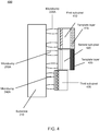
- is a pixel element including sub-pixels bonded on a substrate using microbumps of differing aspect ratios and template layers on the subpixels, in accordance with an embodiment.
- FIG. 5A
- is illustrates Longitudinal Chromatic Aberration (LCA) in a portion of the HMD in
FIG. 1A , in accordance with an embodiment. - FIG. 5B
- illustrates a portion of the HMD in
FIG. 1A configured to mitigate Longitudinal Chromatic Aberration (LCA), in accordance with an embodiment. - FIG. 6
- a portion of the electronic display of
FIG. 1B that includes a plurality of pixel elements configured to mitigate field curvature, in accordance with an embodiment. - The figures depict embodiments of the present disclosure for purposes of illustration only. One skilled in the art will readily recognize from the following description that alternative embodiments of the structures and methods illustrated herein may be employed without departing from the principles, or benefits touted, of the disclosure described herein.
- A head-mounted display (HMD) presents a viewable media to a user. The HMD includes a light source and an optical block. The light source includes a plurality of pixel elements that generate image light corresponding to the viewable media. Each pixel element includes a substrate, one or more sub-pixels, and one or more microbumps of various aspect ratios. In some configurations, each pixel element includes a substrate of a desired thickness formed by micromachining or deposition of additive layers. The light source generates different optical bands of light such as green (e.g. λ = 530 nm), blue (e.g. λ = 470 nm), and red (e.g. λ = 640 nm). In some embodiments, some or all of the microbumps are positioned at a different height in order to mitigate longitudinal chromatic aberration, field curvature, or both.
-
FIG. 1A is a diagram of aHMD 100, in accordance with an embodiment. TheHMD 100 is a head-mounted display that presents content to a user. Example content includes images, video, audio, or some combination thereof. TheHMD 100 includes display elements (not shown inFIG. 1A ), an inertial measurement unit (IMU) 110, and a plurality oflocators 120. The display elements include pixel elements with microbumps of various aspect ratios that mitigate the chromatic aberrations in the image light corresponding to the content presented to the user of theHMD 100, as described below in detail with reference toFIGs. 2-6 . - The
IMU 110 is an electronic device that generates fast calibration data based on measurement signals and generate a plurality of measurement signals in response to motion of theHMD 100. Thelocators 120 are objects located in specific positions on theHMD 100 relative to one another and relative to a specific reference point.Locators 120 may be a light emitting diode (LED), a corner cube reflector, a reflective marker, a type of light source that contrasts with an environment in which theHMD 100 operates, or some combination thereof. -
FIG. 1B is a cross section of theHMD 100 shown inFIG. 1A . As shown inFIG. 1B , theHMD 100 includes display elements that provide image light to theeyebox 160 with mitigated chromatic aberration and field curvature. The cross-section of theHMD 100 includes anelectronic display 130 and anoptical block 140. For purposes of illustration,FIG. 1B shows a cross section of theHMD 100 associated with asingle eye 150, but anotherelectronic display 130, separate from theelectronic display 130, provide altered image light to another eye of the user. - The
electronic display 130 presents visual information (i.e., image light) from an electronic signal. Theelectronic display 130 includes one or more electronic display elements. An electronic display element may be, e.g., a liquid crystal display (LCD), an organic light emitting diode (OLED) display, an active-matrix organic light-emitting diode display (AMOLED), some type of flexible display, or some combination thereof. Theelectronic display 130 includes pixel elements of a variable height to mitigate chromatic aberration, as described below in detail with reference toFIGs. 2-5B . In some configurations, theelectronic display 130 may include pixel elements of variable heights to offset the field curvature, as described below in detail with reference toFIG. 6 .
Theoptical block 140 directs an image light from theelectronic display 130 to aneyebox 160. Theeyebox 160 is a region of space occupied by theeye 150 of the user. Theoptical block 140 includes one or more optical elements composed of materials (e.g., plastic, glass, etc.) with suitable refractive indices that effectively minimize the weight of theHMD 100. The optical elements may act to, e.g., correct aberrations in image light emitted from theelectronic display 130, magnify image light emitted from theelectronic display 130, some other optical adjustment of image light emitted from theelectronic display 130, or some combination thereof. The example for optical elements may include an aperture, a Fresnel lens, a convex lens, a concave lens, a filter, or any other suitable optical element that affects image light. -
FIG. 2 is apixel element 200 including sub-pixels bonded onto asubstrate 210 using a plurality of microbumps of different heights, in accordance with an embodiment. - The
pixel element 200 generates image light to present viewable media to the user's eyes. Thepixel element 200 includes asubstrate 210, amicrobump 220A, amicrobump 220B, amicrobump 230A, amicrobump 230B, amicrobump 240A, amicrobump 240B, afirst sub-pixel 250, afirst emitter 255, asecond sub-pixel 260, asecond emitter 265, athird sub-pixel 270, and athird emitter 275. - The
substrate 210 supports one or more physical components mounted on thesubstrate 210. Thesubstrate 210 may be composed of materials including, but not restricted to, glass, plastic, metal, semiconductor wafer (e.g. silicon, gallium arsenide, gallium nitride, etc.), sapphire, or some combination thereof. In some configurations, thesubstrate 210 may be micromachined or etched (e.g. thinned/polished wet or dry etch, etc.) to achieve a desired thickness of thesubstrate 210. In alternate configurations, one or more additive layers (e.g. dielectric, photoresist, and polyimide) may be deposited on thesubstrate 210 to achieve a desired thickness of thesubstrate 210. - Each of the
microbumps first sub-pixel 250, thesecond sub-pixel 260, and the third sub-pixel 270) to thesubstrate 210. In some configurations, a microbump (e.g., 220A, 220B, 230A, 230B, 240A, and/or 240B) has a cylindrical shape with a variable aspect ratio manufactured by changing the pad design of the substrate or one or more deposition parameters of the method used for depositing the microbump. The shape of the microbump can be cylindrical, annular, trapezoidal or square-shaped with straight angled or rounded side profiles. - In one example, the microbump has a diameter of 3 microns and heights ranging from 3 to 6 microns. In another example, the microbump has a diameter of 5 microns and heights ranging from 5 to 10 microns. The microbump is formed by a solid state bonding of metallic alloys based on deposition methods such as electroplating, electroless deposition, sputtering, physical evaporation, or some combination thereof. The
microbumps - The
first sub-pixel 250 is a light emitting element that emits a light of a first optical band. In some configurations, thefirst sub-pixel 250 is made of GaAs-based heterostructures that emit a red colored light (e.g. λ = 640 nm). Thefirst sub-pixel 250 is mounted on thesubstrate 210 by the microbump 220. In one example, thefirst sub-pixel 250 is mounted on an n-type GaAs substrate of a specific crystal orientation (e.g. 6° off towards the <111> plane). Thefirst emitter 255 is an active region of thefirst sub-pixel 250 that generates the light of the first optical band. In one example, thefirst emitter 255 includes a plurality of quantum well structures (e.g. GaInP/AlGaInP) with a threshold value of thickness (e.g. 10 nm) for each of the quantum wells. Thefirst sub-pixel 250 includes a plurality of light emitting elements. - The
second sub-pixel 260 is a light emitting element that emits a light of a second optical band. In some configurations, thefirst sub-pixel 250 is made of GaN-based heterostructures that emit a green colored light (e.g. λ = 530 nm). Thesecond sub-pixel 260 is mounted on thesubstrate 210 by the microbump 230. In one example, thesecond sub-pixel 260 is mounted on a Sapphire substrate. Thesecond emitter 265 is an active region of thesecond sub-pixel 260 that generates the light of the second optical band. In one example, thesecond emitter 265 includes a plurality of quantum well structures (e.g. InGaN/GaN) with a threshold value of thickness (e.g. 10 nm) for each of the quantum wells. Thesecond sub-pixel 260 includes a plurality of light emitting elements. - The
third sub-pixel 270 is a light emitting element that emits a light of a third optical band. In some configurations, thethird sub-pixel 270 is made of GaN-based heterostructures that emit a blue colored light (e.g. λ = 470 nm). Thethird sub-pixel 270 is mounted on thesubstrate 210 by the microbump 240. In one example, thethird sub-pixel 270 is mounted on a Sapphire substrate. Thethird emitter 275 is an active region of thethird sub-pixel 270 that generates the light of the third optical band. In one example, thethird emitter 275 includes a plurality of quantum well structures (e.g. InGaN/GaN) with a threshold value of thickness (e.g. 10 nm) for each of the quantum wells. Thethird sub-pixel 270 includes a plurality of light emitting elements. - In some configurations, the
third sub-pixel 270 is mounted at a relatively lower height (e.g. 11 microns) when compared to thefirst sub-pixel 250 and thesecond sub-pixel 260. Such a configuration takes into account the relative distance of each of the light emitting elements from theoptical block 140. A conventional pixel element generally has all its sub-pixels mounted at a same height. In contrast, thepixel element 200 has thethird sub-pixel 270 which emits light at a shorter wavelength than light from, e.g., thefirst sub-pixel 250. This difference in height acts to mitigate chromatic aberration that would otherwise occur as light from each of the sub-pixels propagates through an optical system. In one example, themicrobump 220A has a height of 7-10 microns, themicrobump 230A has a height in the range of 7 to 10 microns, and themicrobump 240A has a height of 0 microns. The height difference between each of the threemicrobumps microbumps - In some embodiments, the
pixel element 200 includes one or more sub-pixels. Each of the one or more sub-pixels may be mounted at different heights. For example, thepixel element 200 may include five sub-pixels and at least two of the five sub-pixels may be mounted at two different heights. In some embodiments, each sub-pixel is mounted at height based on what wavelength of light is emitted by the sub-pixel. For example, a sub-pixel that emits red light may be mounted at a first height, a sub-pixel that emits green light is mounted at a second height that is less than the first height, and a sub-pixel that emits blue light is mounted at a third height that is less than the second height. -
FIG. 3 is apixel element 300 including sub-pixels bonded on a raised substrate using aspect ratio microbumps, in accordance with an embodiment. Thepixel element 300 generates image light to present viewable media to the user's eyes. Thepixel element 300 includes a raisedsubstrate 310, themicrobump 220A, themicrobump 220B, themicrobump 230A, themicrobump 230B, themicrobump 240A, themicrobump 240B, thefirst sub-pixel 250, thesecond sub-pixel 260, and thethird sub-pixel 270. - The raised
substrate 310 supports one or more physical components mounted on different portions of the raisedsubstrate 310. The raisedsubstrate 310 is composed of materials including, but not restricted to, glass, plastic, metal, semiconductor wafer (e.g. silicon, gallium arsenide, gallium nitride, etc.), sapphire, or some combination thereof. In some configurations, the raisedsubstrate 310 may be micromachined or etched (e.g. laser lift-off, wet etch, etc.) at different locations to achieve one or more desired thickness at different portions of the raisedsubstrate 310. The raisedsubstrate 310 includes astandoff portion 320 with a thickness in the range of 0 to 11 microns. Thestandoff portion 320 mounts at least one sub-pixel at a specific height relative to the thickness of the raisedsubstrate 310. In the embodiment ofFIG. 3 , thestandoff portion 320 mounts thefirst sub-pixel 250 and thesecond sub-pixel 260 at the same height relative to the thickness of the raisedsubstrate 310. In alternate configurations, thefirst sub-pixel 250 may be mounted at a first standoff portion (not shown here) and thesecond sub-pixel 260 may be mounted at a second standoff portion (not shown here) in order to adjust the position of a sub-pixel relative to the distance from an optical surface. - In the embodiment of
FIG. 3 , thefirst sub-pixel 250 and thesecond sub-pixel 260 are mounted at a first height using themicrobump 220A and themicrobump 230A, while thethird sub-pixel 270 is mounted at a second height using themicrobump 240A on the raisedsubstrate 310. In a different embodiment, thefirst sub-pixel 250 is mounted at a first height using themicrobump 220A and the second sub-pixel is mounted at a second height using themicrobump 230A. For example, the first height is at least 10 microns and the second height is at least 10 microns. Thefirst sub-pixel 250 and thesecond sub-pixel 260 have a pitch in the range of 0 to 1 micron. - In alternate embodiments, one or more additive layers (e.g. dielectric, photoresist, and polyimide) may be deposited on the raised
substrate 310 to achieve a desired thickness of thestandoff portion 320. In one example, thestandoff portion 320 has a thickness in the range of 0 to 20 microns. When compared to micromachining thesubstrate 210 ofFIG. 2 to achieve thestandoff portion 320 of a specific height, deposition of additive layers on the raisedsubstrate 310 achieves thestandoff portion 320 of a precise value of thickness and better uniformity of thickness across thestandoff portion 320 suitable for high volume manufacturing purposes. - In some embodiments, the
pixel element 300 includes one or more sub-pixels. Each of the one or more sub-pixels may be mounted at different heights. For example, thepixel element 300 may include five sub-pixels and at least two of the five sub-pixels may be mounted at two different heights. - The
pixel element 300 ofFIG. 3 is only an example embodiment of a pixel element, and several other variations are possible, using a combination of thepixel element 200 ofFIG. 2 and thepixel element 300 ofFIG. 3 that are not explicitly shown here so as not to unnecessarily obscure aspects of the embodiments. -
FIG. 4 is apixel element 400 including sub-pixels bonded on asubstrate 210 using microbumps of differing aspect ratios and template layers on the subpixels, in accordance with an embodiment. - The
pixel element 400 generates image light to present a viewable media to the user's eyes. Thepixel element 400 includes thesubstrate 210, themicrobump 220A, themicrobump 220B, themicrobump 230A, themicrobump 230B, themicrobump 240A, themicrobump 240B, afirst sub-pixel 410, atemplate layer 415, asecond sub-pixel 420, atemplate layer 425, and athird sub-pixel 430. Thesubstrate 210 may include one or more non-transparent layers that are removed by processes including, but not restricted to, laser lift-off, wet chemical etching, and some combination thereof. - The
first sub-pixel 410 is a light emitting element that emits light of a first optical band. In some configurations, thefirst sub-pixel 410 is made of GaAs-based heterostructures that emit a red colored light (e.g. λ = 640 nm). Thefirst sub-pixel 410 is mounted on thesubstrate 210 by the microbump 220. Thefirst sub-pixel 410 is similar to thefirst sub-pixel 250 ofFIG. 2 except for the presence of atemplate layer 415. - The
template layer 415 is an additional transparent layer added during the growth of thefirst sub-pixel 410 to compensate for the stress due to lattice mismatch with the substrate210. Thetemplate layer 415 is an undoped epitaxial layer selected from a group consisting of: Aluminum Nitride (AlN), Aluminum gallium Nitride (AlGaN), Indium Gallium Nitride (InGaN), Gallium Nitride (GaN), Indium Gallium Arsenide (InGaAs), Indium Gallium Phosphide (InGaP), and some combination thereof. Thetemplate layer 415 can also include one or more non-epitaxial layers which are added after growing thefirst sub-pixel 410. For example, the non-epitaxial layer may include elayers used for our micro assembly processes. The elayers are transparent materials typically made from PDMS (Polydimethylsiloxane). Other options for the elayers include Silicone gel (e.g. Wacker Semicosil 915HT - UV curable, heat resistant up to 210°C), Silopren (e.g. Ultra Clear Silopren LSR 7000) or PI (Polyimide, e.g. Essar Stretch - a type of Polyimide that exhibit optical clarity and temperature stability up to 300°C). They can be molded into shapes at microscale and have good adhesive properties. In some configurations, thetemplate layer 415 is an undoped buffer layer of a threshold value of thickness added during the growth of thefirst sub-pixel 410. For example, the threshold value of thickness of thetemplate layer 415 is in the range of 0.1 micron to four microns. - The
second sub-pixel 420 is a light emitting element that emits a light of a second optical band. In some configurations, thesecond sub-pixel 420 is made of GaN-based heterostructures that emit a green colored light (e.g. λ = 530 nm). Thesecond sub-pixel 420 is mounted on thesubstrate 210 by the microbump 230. Thethird sub-pixel 430 is similar to thesecond sub-pixel 260 ofFIG. 2 except for the presence of atemplate layer 425. - The
template layer 425 is an embodiment of thetemplate layer 415. In some configurations, thetemplate layer 425 is an undoped buffer layer of a threshold value of thickness added during the growth of thesecond sub-pixel 420. For example, the threshold value of thickness of thetemplate layer 425 is in the range of 0.1 micron to 4 microns. - The
third sub-pixel 430 is a light emitting element that emits a light of a third optical band. In some configurations, thethird sub-pixel 430 includes an undoped buffer layer (not shown here) of a threshold value of thickness added during the growth of thethird sub-pixel 430. For example, the threshold value of thickness is in the range of 0.1 micron to 4 microns. - When compared to the embodiments of the
pixel element 200 ofFIG. 2 and thepixel element 300 ofFIG. 3 , thepixel element 400 minimizes the use of high aspect ratio microbumps and also avoids any interference of the pickup head during the placement of thethird sub-pixel 430. The pickup head picks up each of the sub-pixels and place the sub-pixels onto thesubstrate 210. Typically, the pickup head is large and involves getting access or clearance for the placement of sub-pixels. The placement of thethird sub-pixel 430 is done first before the placement of thefirst sub-pixel 410 and thesecond sub-pixel 420. If not done first, the pickup head will be restricted to access and place thethird sub-pixel 430 at the correct placement location because of interference by the neighboringsecond sub-pixel 420. Thetemplate layer 415 minimizes the possibility of interference without the raisedsubstrate 310 of thepixel element 300 ofFIG. 3 and/or the significant difference in aspect ratios of thepixel element 200 ofFIG. 2 . - In alternate embodiments, the
pixel element 400 includes one or more sub-pixels. Each of the one or more sub-pixels can be mounted at different heights. For example, thepixel element 400 may include five sub-pixels and at least two of the five sub-pixels may be mounted at two different heights. - The
pixel element 400 ofFIG. 4 is only an example embodiment of a pixel element, and several other variations are possible, using a combination of thepixel element 200 ofFIG. 2 , thepixel element 300 ofFIG. 3 , and thepixel element 400 ofFIG. 4 that are not explicitly shown here so as not to unnecessarily obscure aspects of the embodiments. For example, thefirst sub-pixel 250 of thepixel element 200 may include thetemplate layer 415 ofFIG. 4 and thefirst sub-pixel 250 may be mounted on thestandoff portion 320 of the raisedsubstrate 310 ofFIG. 3 . -
FIG. 5A is illustrates Longitudinal Chromatic Aberration (LCA) in aportion 500 of the HMD ofFIG. 1A , in accordance with an embodiment. - The
portion 500 includes a portion of theoptical block 505, thesubstrate 210, thefirst sub-pixel 250, thesecond sub-pixel 260, and thethird sub-pixel 270. The portion of theoptical block 505 is an embodiment of theoptical block 140, as described above in conjunction withFIG. 1 . Theoptical block 505 includes anoptical axis 510. - As shown in
FIG. 5A , each of thefirst sub-pixel 250, thesecond sub-pixel 260, and thethird sub-pixel 270 is mounted on thesubstrate 210. Thefirst sub-pixel 250 emitsred light 515 andred light 520 toward the portion of theoptical block 505. The portion of theoptical block 505 directs thered light 515 and thered light 520 with a significant divergence such that the user'seye 150 would see a viewable media corresponding to thered light 515 and thered light 520 at avirtual image plane 535. Thethird sub-pixel 270 emitsblue light 525 andblue light 530 toward the portion of theoptical block 505. The portion of theoptical block 505 directs theblue light 525 and theblue light 530 with a significant divergence such that the user'seye 150 would see a viewable media corresponding to theblue light 525 and theblue light 530 at avirtual image plane 540. The difference in relative positions of thevirtual image plane 535 and thevirtual image plane 540 with reference to theoptical axis 510 results in a longitudinal chromatic aberration when presented to the user'seye 150. -
FIG. 5B illustrates aportion 502 of the HMD inFIG. 1A configured to mitigate Longitudinal Chromatic Aberration (LCA), in accordance with an embodiment. - The
portion 502 includes thefirst sub-pixel 250, thesecond sub-pixel 260, and thethird sub-pixel 270 of thepixel element 200. In some configurations, theportion 502 may include the sub-pixels of thepixel element 300 and thepixel element 400, as described above in conjunction withFIG. 3 andFIG. 4 . In alternate configurations, theportion 502 may include some other pixel element that is designed to correct for LCA for at least two bands of light emitted by the display. - As shown in
FIG. 5B , each of thefirst sub-pixel 250, thesecond sub-pixel 260, and thethird sub-pixel 270 is mounted on thesubstrate 210. Thefirst sub-pixel 250 emits ared light 515 and ared light 520 toward the portion of theoptical block 505. The portion of theoptical block 505 directs thered light 515 and thered light 520 as a plane wave corresponding to a virtual image plane (not shown here) formed at an infinite distance. Thered light 515 and thered light 520 present the viewable media to the user'seye 150 with mitigated longitudinal chromatic aberration as the user'seye 150 interprets the viewable media as the plane wave exiting theportion 502 from an infinite distance. Note that when compared to theportion 500 ofFIG. 5A , theportion 502 includes pixel elements that mitigate the LCA to few tens of microns. Thethird sub-pixel 270 emits ablue light 525 and ablue light 530 toward the portion of theoptical block 505. The portion of theoptical block 505 directs theblue light 525 and theblue light 530 to the same virtual image plane formed at an infinite distance. Theblue light 525 and theblue light 530 present the viewable media to the user'seye 150 with a mitigated longitudinal chromatic aberration. Note that in the embodiment inFIG. 5B , thefirst sub-pixel 250 and thesecond sub-pixel 260 are at the same relative height, but they emit in different bands, accordingly, there may be some longitudinal chromatic aberration. However, in most cases, the amount of aberration is rather minimal between red light and green light, accordingly, in order to, e.g., simplify manufacturing and reduce costs, thefirst sub-pixel 250 and thesecond sub-pixel 260 can be placed at the same relative height. Moreover, as the eye is most sensitive to green light, in some embodiments, the distances from thesubstrate 210 for thefirst sub-pixel 250 and thethird sub-pixel 270 may be set such that the corresponding virtual image planes are co-located with the virtual image plane for the green light emitted from thesecond sub-pixel 260. - In some embodiments, each sub-pixel that emits in particular band of light is positioned at a specific distance from the
substrate 210 to mitigate chromatic aberration for all bands of light. For example, thefirst sub-pixel 250 emits red light and is at a first distance from thesubstrate 210, thesecond sub-pixel 260 emits green light and is at a second distance from thesubstrate 210 that is less than the first distance, and thethird sub-pixel 270 that emits blue light is at a third distance from thesubstrate 210 that is less than the second distance. -
FIG. 6 aportion 600 of theelectronic display 130 ofFIG. 1B that includes a plurality of pixel elements configured to mitigate field curvature, in accordance with an embodiment. Theportion 600 includes apixel element 605 and a portion of theoptical block 610. The portion of theoptical block 610 is an embodiment of theoptical block 140, as described above with reference toFIG. 1B . The portion of theoptical block 610 includes theoptical axis 510, as described above with reference toFIG. 5 . Each of themicrobump microbump 220A, as described above with reference toFIG. 2 . - As shown in
FIG. 6 , each of themicrobump optical block 610. In the example ofFIG. 6 , themicrobump 650 is associated with a specific out-of-plane height 660 (e.g. 6 microns) such that the sub-pixel 680 is separated from the portion of theoptical block 610 by adistance 670. In one example, thedistance 670 is in the range of 100 to 500 microns. Such relative differences between the out-of-plane heights and the distance of separation from the portion of theoptical block 610 compensates for the field curvature of the portion of theoptical block 610. In some configurations, the portion of theoptical block 610 may include lenses with one or more rotationally asymmetric surfaces, and thepixel element 605 may include a plurality of out-of-plane heights (not shown here) to compensate for the differences in radius of curvature of such rotationally asymmetric surfaces. Such a configuration allows compensation for the field curvature of a lens in the portion of theoptical block 610 by adjusting the out-of-plane height 660 of each of the corresponding sub-pixels. The embodiment ofFIG. 6 , simplifies the design of the portion of theoptical block 610 and a relatively smaller lens of the portion of theoptical block 610 can be achieved without sacrificing the quality of the viewable media presented to the user'seye 150. - The foregoing description of the embodiments of the disclosure has been presented for the purpose of illustration; it is not intended to be exhaustive or to limit the disclosure to the precise forms disclosed. Persons skilled in the relevant art can appreciate that many modifications and variations are possible in light of the above disclosure.
- Some portions of this description describe the embodiments of the disclosure in terms of algorithms and symbolic representations of operations on information. These algorithmic descriptions and representations are commonly used by those skilled in the data processing arts to convey the substance of their work effectively to others skilled in the art. These operations, while described functionally, computationally, or logically, are understood to be implemented by computer programs or equivalent electrical circuits, microcode, or the like. Furthermore, it has also proven convenient at times, to refer to these arrangements of operations as modules, without loss of generality. The described operations and their associated modules may be embodied in software, firmware, hardware, or any combinations thereof.
- Any of the steps, operations, or processes described herein may be performed or implemented with one or more hardware or software modules, alone or in combination with other devices. In one embodiment, a software module is implemented with a computer program product comprising a computer-readable medium containing computer program code, which can be executed by a computer processor for performing any or all of the steps, operations, or processes described.
- Embodiments of the disclosure may also relate to an apparatus for performing the operations herein. This apparatus may be specially constructed for the required purposes, and/or it may comprise a general-purpose computing device selectively activated or reconfigured by a computer program stored in the computer. Such a computer program may be stored in a non-transitory, tangible computer readable storage medium, or any type of media suitable for storing electronic instructions, which may be coupled to a computer system bus. Furthermore, any computing systems referred to in the specification may include a single processor or may be architectures employing multiple processor designs for increased computing capability.
- Embodiments of the disclosure may also relate to a product that is produced by a computing process described herein. Such a product may comprise information resulting from a computing process, where the information is stored on a non-transitory, tangible computer readable storage medium and may include any embodiment of a computer program product or other data combination described herein. Finally, the language used in the specification has been principally selected for readability and instructional purposes, and it may not have been selected to delineate or circumscribe the inventive subject matter. It is therefore intended that the scope of the disclosure be limited not by this detailed description, but rather by any claims that issue on an application based hereon. Accordingly, the disclosure of the embodiments is intended to be illustrative, but not limiting, of the scope of the disclosure, which is set forth in the following claims.
Claims (13)
- A head-mounted display, comprising:a light source comprising a plurality of pixel elements configured to emit image light that includes at least two different optical bands of light, the light source further comprising:a first sub-pixel mounted on a first set of microbumps at a first height from a substrate and configured to emit light within a first optical band, anda second sub-pixel mounted on a second set of microbumps at a second height from the substrate that is different from the first height, and the second sub-pixel is configured to emit light over a second optical band that is different than the first optical band, each of the first sub-pixel and the second sub-pixel comprising a plurality of light emitting elements; andan optical block configured to receive the image light from the light source, and direct the image light to an eyebox, wherein the first height and the second height are configured to mitigate longitudinal chromatic aberration in the optical block.
- The head-mounted display of claim 1, wherein the light source includes a third sub-pixel mounted on a third set of microbumps at a third height from the substrate different from the second height, and the third sub-pixel is configured to emit light over a third optical band that is different than the first optical band and the second optical band, the third sub-pixel comprising a plurality of light emitting elements.
- The head-mounted display of claim 2, wherein the substrate is micromachined to a threshold value of thickness at one or more locations on the substrate to mount the third sub-pixel, the threshold value of thickness determined based on the first height and the second height to mitigate longitudinal chromatic aberration in the optical block;
optionally, wherein the threshold value of thickness is achieved by depositing one or more additive layers on the substrate to form one or more standoff portions, each standoff portion mounting at least the first sub-pixel and the second sub-pixel at a fourth height different from the third height to mitigate longitudinal chromatic aberration in the optical block. - The head-mounted display of any of claims 1 to 3, wherein the light source includes a template layer in each of the first sub-pixel and the second sub-pixel, the template layer configured to compensate a stress due to lattice mismatch with the substrate.
- The head-mounted display of any of claims 2 to 4, wherein the third height from the substrate is different from the first height.
- The head-mounted display of any of claims 1 to 5, wherein the first set of microbumps and the second set of microbumps are associated with one or more out-of-plane heights determined based on a distance of separation from the optical block, the difference between the out-of-plane height and the distance of separation compensating for a field curvature of the optical block.
- The head-mounted display of claim 6, wherein the first set of microbumps and the second set of microbumps are mounted on the substrate micromachined to a threshold value of thickness to mitigate longitudinal chromatic aberration in the optical block; and/or
wherein the first set of microbumps mounts the first sub-pixel including a first template layer and the second set of microbumps mounts a second sub-pixel including a second template layer different from the first template layer to mitigate longitudinal chromatic aberration in the optical block. - An electronic display, comprising:a substrate;a plurality of microbumps;a first sub-pixel mounted on a first set of microbumps on the substrate at a first height and configured to emit light within a first optical band ; anda second sub-pixel mounted on a second set of microbumps on the substrate at a second height that is different from the first height, and the second sub-pixel is configured to emit light within a second optical band that is different than the first optical band, wherein the first height and the second height are configured to mitigate longitudinal chromatic aberration in an optical block receiving light from the electronic display, each of the first sub-pixel and the second sub-pixel comprising a plurality of light emitting elements.
- The electronic display of claim 8, further comprising:a third sub-pixel mounted on a third set of microbumps at a third height different from the second height, and the third sub-pixel is configured to emit light over a third optical band that is different than the first optical band and the second optical band, the third sub-pixel comprising a plurality of light emitting elements.
- The electronic display of claim 9, wherein the substrate is micromachined to a threshold value of thickness at one or more locations on the substrate to mount the third sub-pixel, the threshold value of thickness determined based on the first height and the second height to mitigate longitudinal chromatic aberration in the optical block;
optionally, wherein the threshold value of thickness is achieved by depositing one or more additive layers on the substrate to form one or more standoff portions, each standoff portion mounting at least the first sub-pixel and the second sub-pixel at a fourth height different from the third height; and/or wherein the third height from the substrate is different from the first height. - The electronic display of any of claims 8 to 10, wherein the light source includes a template layer in each of the first sub-pixel and the second sub-pixel, the template layer configured to compensate a stress due to lattice mismatch with the substrate.
- The electronic display of any of claims 8 to 11, wherein the first set of microbumps and the second set of microbumps are associated with one or more out-of-plane heights determined based on a distance of separation from the optical block, the difference between the out-of-plane height and the distance of separation compensating for a field curvature of the optical block.
- The electronic display of claim 12, wherein the first set of microbumps and the second set of microbumps are mounted on the substrate micromachined to a threshold value of thickness to mitigate longitudinal chromatic aberration in the optical block; and/or
wherein the first set of microbumps mounts the first sub-pixel including a first template layer and the second set of microbumps mounts a second sub-pixel including a second template layer different from the first template layer to mitigate longitudinal chromatic aberration in the optical block.
Applications Claiming Priority (2)
| Application Number | Priority Date | Filing Date | Title |
|---|---|---|---|
| US15/683,183 US10373936B2 (en) | 2017-08-22 | 2017-08-22 | Pixel elements including light emitters of variable heights |
| PCT/US2018/046084 WO2019040294A1 (en) | 2017-08-22 | 2018-08-09 | Pixel elements including light emitters of variable heights |
Publications (2)
| Publication Number | Publication Date |
|---|---|
| EP3447562A1 true EP3447562A1 (en) | 2019-02-27 |
| EP3447562B1 EP3447562B1 (en) | 2023-07-12 |
Family
ID=65437581
Family Applications (1)
| Application Number | Title | Priority Date | Filing Date |
|---|---|---|---|
| EP18189101.1A Active EP3447562B1 (en) | 2017-08-22 | 2018-08-15 | Pixel elements including light emitters of variable heights |
Country Status (6)
| Country | Link |
|---|---|
| US (1) | US10373936B2 (en) |
| EP (1) | EP3447562B1 (en) |
| JP (1) | JP7142082B2 (en) |
| KR (1) | KR20200035116A (en) |
| CN (1) | CN111108427B (en) |
| WO (1) | WO2019040294A1 (en) |
Families Citing this family (2)
| Publication number | Priority date | Publication date | Assignee | Title |
|---|---|---|---|---|
| KR102510569B1 (en) * | 2017-10-27 | 2023-03-15 | 엘지디스플레이 주식회사 | Organic light emitting display device |
| US11402635B1 (en) * | 2018-05-24 | 2022-08-02 | Facebook Technologies, Llc | Systems and methods for measuring visual refractive error |
Citations (6)
| Publication number | Priority date | Publication date | Assignee | Title |
|---|---|---|---|---|
| US20070297750A1 (en) * | 2006-06-07 | 2007-12-27 | Michael Bass | High resolution, full color, high brightness fully integrated light emitting devices and displays |
| US20100091031A1 (en) * | 2008-10-09 | 2010-04-15 | Canon Kabushiki Kaisha | Image processing apparatus and method, head mounted display, program, and recording medium |
| US20130292831A1 (en) * | 2012-05-03 | 2013-11-07 | Taiwan Semiconductor Manufacturing Company, Ltd. | Methods and Apparatus for Package on Package Devices |
| US9429756B1 (en) * | 2013-06-27 | 2016-08-30 | Google Inc. | Transparent microdisplay in head mountable displays |
| US20160268551A1 (en) * | 2015-03-10 | 2016-09-15 | Oculus Vr, Llc | Reflective layer for increasing fill factor in an electronic display |
| WO2018222688A1 (en) * | 2017-06-02 | 2018-12-06 | Applied Materials, Inc. | Nanostructured flat lenses for display technologies |
Family Cites Families (9)
| Publication number | Priority date | Publication date | Assignee | Title |
|---|---|---|---|---|
| US6392257B1 (en) | 2000-02-10 | 2002-05-21 | Motorola Inc. | Semiconductor structure, semiconductor device, communicating device, integrated circuit, and process for fabricating the same |
| US6809337B2 (en) | 2002-04-22 | 2004-10-26 | Intel Corporation | Liquid crystal display devices having fill holes and electrical contacts on the back side of the die |
| JP4450067B2 (en) | 2007-12-25 | 2010-04-14 | ソニー株式会社 | Electronic component, method for manufacturing the same, and image display apparatus using the same |
| JP5117326B2 (en) | 2008-08-29 | 2013-01-16 | 富士フイルム株式会社 | Color display device and manufacturing method thereof |
| KR20160029245A (en) * | 2014-09-04 | 2016-03-15 | 삼성디스플레이 주식회사 | Head mounted display apparatus |
| US10761327B2 (en) | 2015-11-18 | 2020-09-01 | Facebook Technologies, Llc | Directed display architecture |
| US9779686B2 (en) | 2015-12-15 | 2017-10-03 | Oculus Vr, Llc | Aging compensation for virtual reality headset display device |
| CA3014189A1 (en) | 2016-02-11 | 2017-08-17 | Magic Leap, Inc. | Multi-depth plane display system with reduced switching between depth planes |
| CN106199974A (en) * | 2016-09-28 | 2016-12-07 | 京东方科技集团股份有限公司 | A kind of nearly eye display device |
-
2017
- 2017-08-22 US US15/683,183 patent/US10373936B2/en active Active
-
2018
- 2018-08-09 CN CN201880054911.9A patent/CN111108427B/en active Active
- 2018-08-09 KR KR1020207006485A patent/KR20200035116A/en not_active Ceased
- 2018-08-09 WO PCT/US2018/046084 patent/WO2019040294A1/en not_active Ceased
- 2018-08-09 JP JP2020505889A patent/JP7142082B2/en active Active
- 2018-08-15 EP EP18189101.1A patent/EP3447562B1/en active Active
Patent Citations (6)
| Publication number | Priority date | Publication date | Assignee | Title |
|---|---|---|---|---|
| US20070297750A1 (en) * | 2006-06-07 | 2007-12-27 | Michael Bass | High resolution, full color, high brightness fully integrated light emitting devices and displays |
| US20100091031A1 (en) * | 2008-10-09 | 2010-04-15 | Canon Kabushiki Kaisha | Image processing apparatus and method, head mounted display, program, and recording medium |
| US20130292831A1 (en) * | 2012-05-03 | 2013-11-07 | Taiwan Semiconductor Manufacturing Company, Ltd. | Methods and Apparatus for Package on Package Devices |
| US9429756B1 (en) * | 2013-06-27 | 2016-08-30 | Google Inc. | Transparent microdisplay in head mountable displays |
| US20160268551A1 (en) * | 2015-03-10 | 2016-09-15 | Oculus Vr, Llc | Reflective layer for increasing fill factor in an electronic display |
| WO2018222688A1 (en) * | 2017-06-02 | 2018-12-06 | Applied Materials, Inc. | Nanostructured flat lenses for display technologies |
Also Published As
| Publication number | Publication date |
|---|---|
| JP2020531892A (en) | 2020-11-05 |
| JP7142082B2 (en) | 2022-09-26 |
| US20190067254A1 (en) | 2019-02-28 |
| KR20200035116A (en) | 2020-04-01 |
| CN111108427B (en) | 2022-04-29 |
| US10373936B2 (en) | 2019-08-06 |
| WO2019040294A1 (en) | 2019-02-28 |
| EP3447562B1 (en) | 2023-07-12 |
| CN111108427A (en) | 2020-05-05 |
Similar Documents
| Publication | Publication Date | Title |
|---|---|---|
| US10930529B2 (en) | Formation of elastomeric layer on selective regions of light emitting device | |
| US20220262976A1 (en) | Reducing bowing of materials before wafer-to-wafer bonding for led manufacturing | |
| US12038585B2 (en) | Optical device and method of manufacturing the same | |
| US11575246B2 (en) | Wafer level optic and zoned wafer | |
| US11728318B1 (en) | Micropixellation for alignment-free assembly | |
| KR20220105649A (en) | Light extraction for micro-LEDs | |
| TW202234721A (en) | Self-aligned ito dbr based p-contact for small pitch micro-led | |
| EP3447562B1 (en) | Pixel elements including light emitters of variable heights | |
| US12105288B2 (en) | Augmented reality lenses, and augmented reality glasses and augmented reality system including the same | |
| US11417792B1 (en) | Interconnect with nanotube fitting | |
| KR20220113446A (en) | Left and right projectors for display devices | |
| KR20220140699A (en) | Device including 3D structure for increasing contact surface area for LED | |
| US20240210683A1 (en) | Light source unit and image display device | |
| TW202247483A (en) | Display device and method of manufacturing the same | |
| US20240313166A1 (en) | Light-emitting element, display device including the same and method of fabricating the same | |
| WO2025128688A1 (en) | 3d stack inorganic led architecture | |
| US11195973B1 (en) | III-nitride micro-LEDs on semi-polar oriented GaN | |
| US20260052820A1 (en) | Light emitting element, display device and method for manufacturing the same | |
| US20260020382A1 (en) | Light emitting element, display device, method for manufacturing the same and electronic device | |
| US20250301849A1 (en) | Display device, light emitting element, and method for manufacturing the same | |
| US12546915B1 (en) | Micro-LED beam tuning | |
| US20250336728A1 (en) | Wafer, inspection method for light emitting element, manufacturing method for display device, and inspection device for light emitting element | |
| US20260026171A1 (en) | Display device, method for manufacturing the same and electronic device | |
| US20250311507A1 (en) | Display device and method for manufacturing the same | |
| US20250160064A1 (en) | Light emitting element, display device and method for manufacturing the same |
Legal Events
| Date | Code | Title | Description |
|---|---|---|---|
| PUAI | Public reference made under article 153(3) epc to a published international application that has entered the european phase |
Free format text: ORIGINAL CODE: 0009012 |
|
| STAA | Information on the status of an ep patent application or granted ep patent |
Free format text: STATUS: THE APPLICATION HAS BEEN PUBLISHED |
|
| AK | Designated contracting states |
Kind code of ref document: A1 Designated state(s): AL AT BE BG CH CY CZ DE DK EE ES FI FR GB GR HR HU IE IS IT LI LT LU LV MC MK MT NL NO PL PT RO RS SE SI SK SM TR |
|
| AX | Request for extension of the european patent |
Extension state: BA ME |
|
| STAA | Information on the status of an ep patent application or granted ep patent |
Free format text: STATUS: REQUEST FOR EXAMINATION WAS MADE |
|
| 17P | Request for examination filed |
Effective date: 20190815 |
|
| RBV | Designated contracting states (corrected) |
Designated state(s): AL AT BE BG CH CY CZ DE DK EE ES FI FR GB GR HR HU IE IS IT LI LT LU LV MC MK MT NL NO PL PT RO RS SE SI SK SM TR |
|
| STAA | Information on the status of an ep patent application or granted ep patent |
Free format text: STATUS: EXAMINATION IS IN PROGRESS |
|
| 17Q | First examination report despatched |
Effective date: 20220401 |
|
| GRAP | Despatch of communication of intention to grant a patent |
Free format text: ORIGINAL CODE: EPIDOSNIGR1 |
|
| STAA | Information on the status of an ep patent application or granted ep patent |
Free format text: STATUS: GRANT OF PATENT IS INTENDED |
|
| INTG | Intention to grant announced |
Effective date: 20230203 |
|
| GRAS | Grant fee paid |
Free format text: ORIGINAL CODE: EPIDOSNIGR3 |
|
| GRAA | (expected) grant |
Free format text: ORIGINAL CODE: 0009210 |
|
| STAA | Information on the status of an ep patent application or granted ep patent |
Free format text: STATUS: THE PATENT HAS BEEN GRANTED |
|
| P01 | Opt-out of the competence of the unified patent court (upc) registered |
Effective date: 20230525 |
|
| AK | Designated contracting states |
Kind code of ref document: B1 Designated state(s): AL AT BE BG CH CY CZ DE DK EE ES FI FR GB GR HR HU IE IS IT LI LT LU LV MC MK MT NL NO PL PT RO RS SE SI SK SM TR |
|
| REG | Reference to a national code |
Ref country code: CH Ref legal event code: EP |
|
| REG | Reference to a national code |
Ref country code: IE Ref legal event code: FG4D |
|
| REG | Reference to a national code |
Ref country code: DE Ref legal event code: R096 Ref document number: 602018053111 Country of ref document: DE |
|
| REG | Reference to a national code |
Ref country code: LT Ref legal event code: MG9D |
|
| REG | Reference to a national code |
Ref country code: NL Ref legal event code: MP Effective date: 20230712 |
|
| RAP4 | Party data changed (patent owner data changed or rights of a patent transferred) |
Owner name: META PLATFORMS TECHNOLOGIES, LLC |
|
| REG | Reference to a national code |
Ref country code: AT Ref legal event code: MK05 Ref document number: 1587761 Country of ref document: AT Kind code of ref document: T Effective date: 20230712 |
|
| PG25 | Lapsed in a contracting state [announced via postgrant information from national office to epo] |
Ref country code: NL Free format text: LAPSE BECAUSE OF FAILURE TO SUBMIT A TRANSLATION OF THE DESCRIPTION OR TO PAY THE FEE WITHIN THE PRESCRIBED TIME-LIMIT Effective date: 20230712 |
|
| PG25 | Lapsed in a contracting state [announced via postgrant information from national office to epo] |
Ref country code: GR Free format text: LAPSE BECAUSE OF FAILURE TO SUBMIT A TRANSLATION OF THE DESCRIPTION OR TO PAY THE FEE WITHIN THE PRESCRIBED TIME-LIMIT Effective date: 20231013 |
|
| PG25 | Lapsed in a contracting state [announced via postgrant information from national office to epo] |
Ref country code: ES Free format text: LAPSE BECAUSE OF FAILURE TO SUBMIT A TRANSLATION OF THE DESCRIPTION OR TO PAY THE FEE WITHIN THE PRESCRIBED TIME-LIMIT Effective date: 20230712 |
|
| PG25 | Lapsed in a contracting state [announced via postgrant information from national office to epo] |
Ref country code: IS Free format text: LAPSE BECAUSE OF FAILURE TO SUBMIT A TRANSLATION OF THE DESCRIPTION OR TO PAY THE FEE WITHIN THE PRESCRIBED TIME-LIMIT Effective date: 20231112 |
|
| PG25 | Lapsed in a contracting state [announced via postgrant information from national office to epo] |
Ref country code: SE Free format text: LAPSE BECAUSE OF FAILURE TO SUBMIT A TRANSLATION OF THE DESCRIPTION OR TO PAY THE FEE WITHIN THE PRESCRIBED TIME-LIMIT Effective date: 20230712 Ref country code: RS Free format text: LAPSE BECAUSE OF FAILURE TO SUBMIT A TRANSLATION OF THE DESCRIPTION OR TO PAY THE FEE WITHIN THE PRESCRIBED TIME-LIMIT Effective date: 20230712 Ref country code: PT Free format text: LAPSE BECAUSE OF FAILURE TO SUBMIT A TRANSLATION OF THE DESCRIPTION OR TO PAY THE FEE WITHIN THE PRESCRIBED TIME-LIMIT Effective date: 20231113 Ref country code: NO Free format text: LAPSE BECAUSE OF FAILURE TO SUBMIT A TRANSLATION OF THE DESCRIPTION OR TO PAY THE FEE WITHIN THE PRESCRIBED TIME-LIMIT Effective date: 20231012 Ref country code: LV Free format text: LAPSE BECAUSE OF FAILURE TO SUBMIT A TRANSLATION OF THE DESCRIPTION OR TO PAY THE FEE WITHIN THE PRESCRIBED TIME-LIMIT Effective date: 20230712 Ref country code: LT Free format text: LAPSE BECAUSE OF FAILURE TO SUBMIT A TRANSLATION OF THE DESCRIPTION OR TO PAY THE FEE WITHIN THE PRESCRIBED TIME-LIMIT Effective date: 20230712 Ref country code: IS Free format text: LAPSE BECAUSE OF FAILURE TO SUBMIT A TRANSLATION OF THE DESCRIPTION OR TO PAY THE FEE WITHIN THE PRESCRIBED TIME-LIMIT Effective date: 20231112 Ref country code: HR Free format text: LAPSE BECAUSE OF FAILURE TO SUBMIT A TRANSLATION OF THE DESCRIPTION OR TO PAY THE FEE WITHIN THE PRESCRIBED TIME-LIMIT Effective date: 20230712 Ref country code: GR Free format text: LAPSE BECAUSE OF FAILURE TO SUBMIT A TRANSLATION OF THE DESCRIPTION OR TO PAY THE FEE WITHIN THE PRESCRIBED TIME-LIMIT Effective date: 20231013 Ref country code: FI Free format text: LAPSE BECAUSE OF FAILURE TO SUBMIT A TRANSLATION OF THE DESCRIPTION OR TO PAY THE FEE WITHIN THE PRESCRIBED TIME-LIMIT Effective date: 20230712 Ref country code: ES Free format text: LAPSE BECAUSE OF FAILURE TO SUBMIT A TRANSLATION OF THE DESCRIPTION OR TO PAY THE FEE WITHIN THE PRESCRIBED TIME-LIMIT Effective date: 20230712 Ref country code: AT Free format text: LAPSE BECAUSE OF FAILURE TO SUBMIT A TRANSLATION OF THE DESCRIPTION OR TO PAY THE FEE WITHIN THE PRESCRIBED TIME-LIMIT Effective date: 20230712 |
|
| PG25 | Lapsed in a contracting state [announced via postgrant information from national office to epo] |
Ref country code: PL Free format text: LAPSE BECAUSE OF FAILURE TO SUBMIT A TRANSLATION OF THE DESCRIPTION OR TO PAY THE FEE WITHIN THE PRESCRIBED TIME-LIMIT Effective date: 20230712 |
|
| REG | Reference to a national code |
Ref country code: CH Ref legal event code: PL |
|
| REG | Reference to a national code |
Ref country code: DE Ref legal event code: R097 Ref document number: 602018053111 Country of ref document: DE |
|
| PG25 | Lapsed in a contracting state [announced via postgrant information from national office to epo] |
Ref country code: LU Free format text: LAPSE BECAUSE OF NON-PAYMENT OF DUE FEES Effective date: 20230815 |
|
| PG25 | Lapsed in a contracting state [announced via postgrant information from national office to epo] |
Ref country code: SM Free format text: LAPSE BECAUSE OF FAILURE TO SUBMIT A TRANSLATION OF THE DESCRIPTION OR TO PAY THE FEE WITHIN THE PRESCRIBED TIME-LIMIT Effective date: 20230712 Ref country code: RO Free format text: LAPSE BECAUSE OF FAILURE TO SUBMIT A TRANSLATION OF THE DESCRIPTION OR TO PAY THE FEE WITHIN THE PRESCRIBED TIME-LIMIT Effective date: 20230712 Ref country code: LU Free format text: LAPSE BECAUSE OF NON-PAYMENT OF DUE FEES Effective date: 20230815 Ref country code: EE Free format text: LAPSE BECAUSE OF FAILURE TO SUBMIT A TRANSLATION OF THE DESCRIPTION OR TO PAY THE FEE WITHIN THE PRESCRIBED TIME-LIMIT Effective date: 20230712 Ref country code: DK Free format text: LAPSE BECAUSE OF FAILURE TO SUBMIT A TRANSLATION OF THE DESCRIPTION OR TO PAY THE FEE WITHIN THE PRESCRIBED TIME-LIMIT Effective date: 20230712 Ref country code: CZ Free format text: LAPSE BECAUSE OF FAILURE TO SUBMIT A TRANSLATION OF THE DESCRIPTION OR TO PAY THE FEE WITHIN THE PRESCRIBED TIME-LIMIT Effective date: 20230712 Ref country code: CH Free format text: LAPSE BECAUSE OF NON-PAYMENT OF DUE FEES Effective date: 20230831 Ref country code: SK Free format text: LAPSE BECAUSE OF FAILURE TO SUBMIT A TRANSLATION OF THE DESCRIPTION OR TO PAY THE FEE WITHIN THE PRESCRIBED TIME-LIMIT Effective date: 20230712 Ref country code: MC Free format text: LAPSE BECAUSE OF FAILURE TO SUBMIT A TRANSLATION OF THE DESCRIPTION OR TO PAY THE FEE WITHIN THE PRESCRIBED TIME-LIMIT Effective date: 20230712 |
|
| REG | Reference to a national code |
Ref country code: BE Ref legal event code: MM Effective date: 20230831 |
|
| PLBE | No opposition filed within time limit |
Free format text: ORIGINAL CODE: 0009261 |
|
| STAA | Information on the status of an ep patent application or granted ep patent |
Free format text: STATUS: NO OPPOSITION FILED WITHIN TIME LIMIT |
|
| REG | Reference to a national code |
Ref country code: IE Ref legal event code: MM4A |
|
| PG25 | Lapsed in a contracting state [announced via postgrant information from national office to epo] |
Ref country code: IT Free format text: LAPSE BECAUSE OF FAILURE TO SUBMIT A TRANSLATION OF THE DESCRIPTION OR TO PAY THE FEE WITHIN THE PRESCRIBED TIME-LIMIT Effective date: 20230712 |
|
| 26N | No opposition filed |
Effective date: 20240415 |
|
| PG25 | Lapsed in a contracting state [announced via postgrant information from national office to epo] |
Ref country code: IE Free format text: LAPSE BECAUSE OF NON-PAYMENT OF DUE FEES Effective date: 20230815 |
|
| PG25 | Lapsed in a contracting state [announced via postgrant information from national office to epo] |
Ref country code: IE Free format text: LAPSE BECAUSE OF NON-PAYMENT OF DUE FEES Effective date: 20230815 Ref country code: FR Free format text: LAPSE BECAUSE OF NON-PAYMENT OF DUE FEES Effective date: 20230912 Ref country code: SI Free format text: LAPSE BECAUSE OF FAILURE TO SUBMIT A TRANSLATION OF THE DESCRIPTION OR TO PAY THE FEE WITHIN THE PRESCRIBED TIME-LIMIT Effective date: 20230712 |
|
| PG25 | Lapsed in a contracting state [announced via postgrant information from national office to epo] |
Ref country code: BE Free format text: LAPSE BECAUSE OF NON-PAYMENT OF DUE FEES Effective date: 20230831 |
|
| PGFP | Annual fee paid to national office [announced via postgrant information from national office to epo] |
Ref country code: DE Payment date: 20240830 Year of fee payment: 7 |
|
| PGFP | Annual fee paid to national office [announced via postgrant information from national office to epo] |
Ref country code: GB Payment date: 20240830 Year of fee payment: 7 |
|
| PG25 | Lapsed in a contracting state [announced via postgrant information from national office to epo] |
Ref country code: BG Free format text: LAPSE BECAUSE OF FAILURE TO SUBMIT A TRANSLATION OF THE DESCRIPTION OR TO PAY THE FEE WITHIN THE PRESCRIBED TIME-LIMIT Effective date: 20230712 |
|
| REG | Reference to a national code |
Ref country code: DE Ref legal event code: R081 Ref document number: 602018053111 Country of ref document: DE Owner name: META PLATFORMS TECHNOLOGIES, LLC, MENLO PARK, US Free format text: FORMER OWNER: FACEBOOK TECHNOLOGIES, LLC, MENLO PARK, CA, US |
|
| PG25 | Lapsed in a contracting state [announced via postgrant information from national office to epo] |
Ref country code: BG Free format text: LAPSE BECAUSE OF FAILURE TO SUBMIT A TRANSLATION OF THE DESCRIPTION OR TO PAY THE FEE WITHIN THE PRESCRIBED TIME-LIMIT Effective date: 20230712 |
|
| PG25 | Lapsed in a contracting state [announced via postgrant information from national office to epo] |
Ref country code: CY Free format text: LAPSE BECAUSE OF FAILURE TO SUBMIT A TRANSLATION OF THE DESCRIPTION OR TO PAY THE FEE WITHIN THE PRESCRIBED TIME-LIMIT; INVALID AB INITIO Effective date: 20180815 |
|
| PG25 | Lapsed in a contracting state [announced via postgrant information from national office to epo] |
Ref country code: HU Free format text: LAPSE BECAUSE OF FAILURE TO SUBMIT A TRANSLATION OF THE DESCRIPTION OR TO PAY THE FEE WITHIN THE PRESCRIBED TIME-LIMIT; INVALID AB INITIO Effective date: 20180815 |
|
| PG25 | Lapsed in a contracting state [announced via postgrant information from national office to epo] |
Ref country code: TR Free format text: LAPSE BECAUSE OF FAILURE TO SUBMIT A TRANSLATION OF THE DESCRIPTION OR TO PAY THE FEE WITHIN THE PRESCRIBED TIME-LIMIT Effective date: 20230712 |
|
| REG | Reference to a national code |
Ref country code: DE Ref legal event code: R119 Ref document number: 602018053111 Country of ref document: DE |
|
| GBPC | Gb: european patent ceased through non-payment of renewal fee |
Effective date: 20250815 |