EP3442078A1 - Structural multilayer antenna design and fabrication - Google Patents
Structural multilayer antenna design and fabrication Download PDFInfo
- Publication number
- EP3442078A1 EP3442078A1 EP18186238.4A EP18186238A EP3442078A1 EP 3442078 A1 EP3442078 A1 EP 3442078A1 EP 18186238 A EP18186238 A EP 18186238A EP 3442078 A1 EP3442078 A1 EP 3442078A1
- Authority
- EP
- European Patent Office
- Prior art keywords
- sheet
- antenna
- top surface
- aircraft
- layer
- Prior art date
- Legal status (The legal status is an assumption and is not a legal conclusion. Google has not performed a legal analysis and makes no representation as to the accuracy of the status listed.)
- Granted
Links
Images


Classifications
-
- H—ELECTRICITY
- H01—ELECTRIC ELEMENTS
- H01Q—ANTENNAS, i.e. RADIO AERIALS
- H01Q1/00—Details of, or arrangements associated with, antennas
- H01Q1/36—Structural form of radiating elements, e.g. cone, spiral, umbrella; Particular materials used therewith
- H01Q1/38—Structural form of radiating elements, e.g. cone, spiral, umbrella; Particular materials used therewith formed by a conductive layer on an insulating support
-
- H—ELECTRICITY
- H01—ELECTRIC ELEMENTS
- H01Q—ANTENNAS, i.e. RADIO AERIALS
- H01Q1/00—Details of, or arrangements associated with, antennas
- H01Q1/27—Adaptation for use in or on movable bodies
- H01Q1/28—Adaptation for use in or on aircraft, missiles, satellites, or balloons
- H01Q1/286—Adaptation for use in or on aircraft, missiles, satellites, or balloons substantially flush mounted with the skin of the craft
-
- B—PERFORMING OPERATIONS; TRANSPORTING
- B64—AIRCRAFT; AVIATION; COSMONAUTICS
- B64C—AEROPLANES; HELICOPTERS
- B64C1/00—Fuselages; Constructional features common to fuselages, wings, stabilising surfaces or the like
- B64C1/06—Frames; Stringers; Longerons ; Fuselage sections
- B64C1/12—Construction or attachment of skin panels
-
- B—PERFORMING OPERATIONS; TRANSPORTING
- B64—AIRCRAFT; AVIATION; COSMONAUTICS
- B64C—AEROPLANES; HELICOPTERS
- B64C3/00—Wings
- B64C3/26—Construction, shape, or attachment of separate skins, e.g. panels
-
- H—ELECTRICITY
- H01—ELECTRIC ELEMENTS
- H01Q—ANTENNAS, i.e. RADIO AERIALS
- H01Q1/00—Details of, or arrangements associated with, antennas
- H01Q1/12—Supports; Mounting means
- H01Q1/1207—Supports; Mounting means for fastening a rigid aerial element
-
- H—ELECTRICITY
- H01—ELECTRIC ELEMENTS
- H01Q—ANTENNAS, i.e. RADIO AERIALS
- H01Q1/00—Details of, or arrangements associated with, antennas
- H01Q1/12—Supports; Mounting means
- H01Q1/22—Supports; Mounting means by structural association with other equipment or articles
-
- H—ELECTRICITY
- H01—ELECTRIC ELEMENTS
- H01Q—ANTENNAS, i.e. RADIO AERIALS
- H01Q1/00—Details of, or arrangements associated with, antennas
- H01Q1/27—Adaptation for use in or on movable bodies
- H01Q1/28—Adaptation for use in or on aircraft, missiles, satellites, or balloons
- H01Q1/286—Adaptation for use in or on aircraft, missiles, satellites, or balloons substantially flush mounted with the skin of the craft
- H01Q1/287—Adaptation for use in or on aircraft, missiles, satellites, or balloons substantially flush mounted with the skin of the craft integrated in a wing or a stabiliser
-
- H—ELECTRICITY
- H01—ELECTRIC ELEMENTS
- H01Q—ANTENNAS, i.e. RADIO AERIALS
- H01Q1/00—Details of, or arrangements associated with, antennas
- H01Q1/40—Radiating elements coated with or embedded in protective material
-
- H—ELECTRICITY
- H01—ELECTRIC ELEMENTS
- H01Q—ANTENNAS, i.e. RADIO AERIALS
- H01Q21/00—Antenna arrays or systems
-
- H—ELECTRICITY
- H01—ELECTRIC ELEMENTS
- H01Q—ANTENNAS, i.e. RADIO AERIALS
- H01Q3/00—Arrangements for changing or varying the orientation or the shape of the directional pattern of the waves radiated from an antenna or antenna system
- H01Q3/26—Arrangements for changing or varying the orientation or the shape of the directional pattern of the waves radiated from an antenna or antenna system varying the relative phase or relative amplitude of energisation between two or more active radiating elements; varying the distribution of energy across a radiating aperture
Definitions
- This disclosure pertains to the structure and fabrication of a multilayer antenna design, more specifically a phased array antenna, embedded inside a structural panel of an aircraft.
- a typical antenna system can be very large and heavy.
- a typical phased array antenna system can be 6' long, 18" tall and 11 ⁇ 2" thick.
- the antenna system itself and the support structure required for the antenna system can occupy a substantial portion of the internal volume of the aircraft. If such an antenna system and its required support structure is attached to the exterior of the aircraft, they can add substantial drag to the aircraft.
- the structural multilayer antenna design of this disclosure and its fabrication overcome the disadvantages of integrating a phase array antenna and its support structure in the interior volume of an aircraft or attaching the antenna and its support structure to the exterior of the aircraft.
- the antenna of this disclosure is embedded inside a structural panel of an aircraft.
- the structural panel could be a panel of the fuselage construction of the aircraft, a panel of a wing construction of the aircraft, a panel of a tail rudder construction of the aircraft, or other similar structural panels.
- the antenna does not require any of the interior volume of the aircraft, it does not require any support structure, and it does not create a source of drag on the exterior of the aircraft.
- a first sheet of a radio frequency (RF) penetrable structural material such as fiberglass is formed.
- RF radio frequency
- Other materials such as cyanate ester resin prepreg fabric, Astroquartz (Astroquartz is a registered trademark of J.P. Stevens & Co., Inc.), and other equivalent materials could be used to form the first sheet.
- the first sheet is rigid and has a curved configuration with a generally convex top surface and a generally concave bottom surface. The curved configuration of the first sheet is determined to match the curved configuration of the aircraft component the structural panel is to become a part of.
- a first antenna layer of electrically conductive material is fixed to the top surface of the first sheet.
- the electrically conductive material could be copper foil.
- a distribution layer of electrically conductive material is fixed to the bottom surface of the first sheet.
- the distribution layer could also be a copper foil fixed to the bottom surface.
- a first antenna configuration is etched into the first antenna layer.
- a distribution configuration is etched into the distribution layer.
- a second sheet for the structural panel is also formed from fiberglass.
- the second sheet is rigid and has a curved configuration with a generally convex top surface and a generally concave bottom surface.
- a second antenna layer of electrically conductive material is fixed to the bottom surface of the second sheet.
- the second antenna layer could be of copper foil.
- a second antenna configuration is etched into the second antenna layer.
- any practical combination of antenna layers and distribution layers could be used in the structural panel of the aircraft.
- the vias can be formed through all of the layers.
- the vias can enable electrical connections between antenna layers, electrical connections between antenna layers and distribution layers, etc.
- the vias can also be used as "gates" around features to isolate those features.
- the first sheet and the second sheet are positioned relative to each other or are registered relative to each other for creating a phased array antenna from the first antenna layer and the second antenna layer.
- the first sheet and the second sheet are positioned in a molding apparatus that is operable to perform a stamp forming process.
- the first sheet and the second sheet are then secured together using the stamp forming process with the top surface of the second sheet engaging against the bottom surface of the first sheet, creating a phased array antenna inside a structural panel of an aircraft.
- the above described method creates a phased array antenna comprising a first antenna layer and a second antenna layer embedded inside a structural panel of an aircraft.
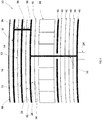
- Figure 1 is a schematic representation of a cross-section view of a portion of a phased array antenna embedded inside a structural panel 10 of an aircraft fabricated according to the method of this disclosure.
- Figure 6 is a schematic representation of a perspective view of the portion of the structural panel 10 represented in Figure 1 .
- the structural panel 10 could be a panel of the fuselage construction of the aircraft, a panel 10 of a wing construction of the aircraft, a panel 10 of a tail rudder construction of the aircraft, or a panel of other structural panels of the overall aircraft construction.
- a first sheet of fiberglass 12 is formed.
- a high strength fiberglass such as Astroquartz fiberglass produced by JPS Composite Materials, a subsidiary of JPS Industries, Inc. is used to form the first sheet 12.
- the first sheet 12 is represented as having a general rectangular configuration in Figure 2
- the first sheet 12 could have any configuration that would match the configuration of the structural component part of the aircraft panel constructed according to the method described herein.
- the first sheet 12 is represented as being generally flat in Figure 2
- the first sheet 12 could in most applications have a curved configuration that matches the curved configuration of the structural component part of the aircraft the panel is to become a part of.
- Such a first sheet 12 constructed of fiberglass is rigid and has a curved configuration.
- a top surface 14 of the first sheet has a general convex configuration and the bottom surface 16 of the first sheet 12 has a general concave configuration.
- the first antenna layer 18 has the same configuration as the first sheet 12.
- the first antenna layer 18 is constructed of electrically conductive material that is often used in the construction of antennas, for example copper foil.
- the distribution network layer 22 has the same configuration as the first sheet 12.
- the distribution network layer 22 is also constructed of electrically conductive material that is often used in the construction of antennas, for example copper foil.
- Figure 3 is a representation of fixing the first antenna layer 18 to the top surface 14 of the first sheet 12, and fixing the distribution network layer 22 to the bottom surface 16 of the first sheet 12.
- the first antenna layer 18 and the distribution network layer 22 can be fixed to the opposite surfaces of the first sheet 12 according to any of the known methods and processes used in the production of a printed circuit board.
- a desired antenna configuration is formed into the first antenna layer 18 on the first sheet 12, and a desired distribution network configuration is formed in the distribution network layer 22 on the first sheet 12.
- the first antenna configuration can be formed into the first antenna layer 18 by any of the known methods and processes used in the production of a printed circuit board. For example, an ultraviolet light sensitive film or a photo "resist” film is applied and secured to the first antenna layer 18 on the first sheet 12 by the application of heat and pressure. An image film having the desired configuration of the first antenna layer is then applied over the "resist" film.
- the first antenna layer 18 is then exposed to high intensity ultraviolet light.
- the ultraviolet light passes through clear areas of the image film and hardens portions of the "resist" film that are not covered by the dark areas of the image film.
- the portions of the "resist” layer that are not hardened by the ultraviolet light are then removed. This exposes portions of the first antenna layer electrically conductive material that are not covered by the hardened "resist”.
- the exposed portions of the electrically conductive material of the first antenna layer are then removed chemically as represented by the areas 24 in Figure 4 , thereby etching the desired first antenna configuration into the first antenna layer.
- the hardened "resist” is then removed, exposing the configuration of the first antenna layer 18 on the top surface 14 of the first sheet 12.
- the distribution network configuration is formed in the distribution network layer 22 in the same manner discussed above with regard to the first antenna layer 18 configuration.
- the above method steps produce the first antenna layer 18, the first sheet 12 of fiberglass and the distribution network layer 22 represented in Figure 5 .
- a second sheet 26 of high strength fiberglass is then formed.
- the second sheet 26 has the same configuration as the first sheet 12, and is constructed in substantially the same manner.
- the second sheet 26 is also rigid and has a curved configuration with a top surface 28 having a general convex configuration and an opposite bottom surface 32 having a general concave configuration.
- a second antenna layer 34 of electrically conductive material for example copper foil, is fixed to the bottom surface 32 of the second sheet 26.
- a desired second antenna configuration is etched into the second antenna layer 34.
- Inter-laminar feeds or vias 36 are formed through first sheet 12, and the second sheet 26.
- the vias 36 are provided to enable electric communication between the first antenna layer 18, the distribution network layer 22 and the second antenna layer 34.
- the first sheet 12 and the second sheet 26 are then registered relative to each other or are positioned relative to each other in the positions they will occupy in the final construction of the phased array antenna inside the panel 10 of the aircraft.
- Electrical communicators 38 are passed through vias 36 and communicate with the first antenna layer 18 and the second antenna layer 34, providing electrical communications between the two antenna layers.
- the distribution network layer 22 is capacitively coupled to the first antenna layer 18 and the second antenna layer 34.
- FIG. 5 is a schematic representation of a molding apparatus comprising a mold 40 and a press 42.
- the first sheet 12 and the second sheet 26, together with the first antenna layer 18, the second antenna layer 34, the distribution network layer 22 all communicating through the electrical communicators 38 are positioned in the mold 40.
- the press 42 is then lowered into the mold 40 applying pressure to the first sheet 12 and the second sheet 26 while the mold 40 heats the first sheet 12 and the second sheet 26.
- the first sheet 12 and the second sheet 26 are then secured together using the stamp forming process, for example a thermoset stamp forming process, with the top surface 28 of the second sheet 26 engaging against the bottom surface 16 of the first sheet 12, creating a phased array antenna inside a structural panel 10 of an aircraft.
- the stamp forming process for example a thermoset stamp forming process
- the first sheet 12 and the second sheet 26 that have been cured together can then be secured to an open cell core panel 44 of the structural panel 10 of the aircraft.
- Additional structural sheets 46 (referred to herein as a "third sheet 46") are also represented in Figure 1 .
- These additional structural sheets 46 could be additional layers of fiberglass or other equivalent materials employed in the construction of the structural panel 10, depending on the intended use of the structural panel 10 in the aircraft.
- Each third sheet 46 includes a top surface and a bottom surface.
- a protective cover layer 48 could be applied to the structural panel 10 to protect the antenna inside the panel.
- the structural panel 10 has been described above as having a first antenna layer 18 and a second antenna layer 34, the panel 10 could be comprised of additional antenna layers and additional distribution layers.
- the antenna layers and the distribution layers of the antenna would all be communicated by electrical communicators 52 that extend through the core panel 44 and the additional structural sheets 46 to an electrical connector interface 54.
- the method 100 of embedding an antenna inside a structural panel of an aircraft includes forming 102 a first sheet from fiberglass with the first sheet being rigid and having a top surface and an opposite bottom surface.
- the top surface could be formed as a convex configuration with the first sheet having a bottom surface that has a concave configuration.
- a first antenna layer of electrically conductive material is then fixed 104 to the top surface of the first sheet.
- the conductive material can be, for example, copper foil.
- a distribution network layer of electrically conductive material can then be fixed 106 to the bottom surface of the first sheet.
- the conductive material can be, for example, copper foil.
- the method 100 further includes etching 108 a first antenna configuration into the first antenna layer and etching 110 a distribution network configuration into the distribution network layer.
- a second sheet from fiberglass is formed 112 with the second sheet being rigid and having a top surface and an opposite bottom surface. The top surface can have a convex configuration and the bottom surface can have a concave configuration.
- a second antenna layer of electrically conductive material is then fixed 114 to the bottom surface of the second sheet.
- the conductive material can be, for example, copper foil.
- the method further includes etching 116 a second antenna configuration into the second antenna layer and securing 118 the first sheet to the second sheet with the bottom surface of the first sheet engaging with the top surface of the second sheet.
Landscapes
- Engineering & Computer Science (AREA)
- Aviation & Aerospace Engineering (AREA)
- Physics & Mathematics (AREA)
- Astronomy & Astrophysics (AREA)
- General Physics & Mathematics (AREA)
- Remote Sensing (AREA)
- Mechanical Engineering (AREA)
- Details Of Aerials (AREA)
- Casting Or Compression Moulding Of Plastics Or The Like (AREA)
- Production Of Multi-Layered Print Wiring Board (AREA)
- Structure Of Printed Boards (AREA)
- Variable-Direction Aerials And Aerial Arrays (AREA)
Abstract
Description
- This disclosure pertains to the structure and fabrication of a multilayer antenna design, more specifically a phased array antenna, embedded inside a structural panel of an aircraft.
- The construction of a typical antenna system, and specifically a phased array antenna system, can be very large and heavy. A typical phased array antenna system can be 6' long, 18" tall and 1½" thick. When such an antenna system is integrated into an aircraft, the antenna system itself and the support structure required for the antenna system can occupy a substantial portion of the internal volume of the aircraft. If such an antenna system and its required support structure is attached to the exterior of the aircraft, they can add substantial drag to the aircraft.
- The structural multilayer antenna design of this disclosure and its fabrication overcome the disadvantages of integrating a phase array antenna and its support structure in the interior volume of an aircraft or attaching the antenna and its support structure to the exterior of the aircraft.
- The antenna of this disclosure is embedded inside a structural panel of an aircraft. The structural panel could be a panel of the fuselage construction of the aircraft, a panel of a wing construction of the aircraft, a panel of a tail rudder construction of the aircraft, or other similar structural panels. By being fabricated in a structural panel of the aircraft, the antenna does not require any of the interior volume of the aircraft, it does not require any support structure, and it does not create a source of drag on the exterior of the aircraft.
- In the method of constructing the antenna embedded inside a structural panel of an aircraft, a first sheet of a radio frequency (RF) penetrable structural material, such as fiberglass is formed. Other materials such as cyanate ester resin prepreg fabric, Astroquartz (Astroquartz is a registered trademark of J.P. Stevens & Co., Inc.), and other equivalent materials could be used to form the first sheet. The first sheet is rigid and has a curved configuration with a generally convex top surface and a generally concave bottom surface. The curved configuration of the first sheet is determined to match the curved configuration of the aircraft component the structural panel is to become a part of.
- A first antenna layer of electrically conductive material is fixed to the top surface of the first sheet. The electrically conductive material could be copper foil.
- A distribution layer of electrically conductive material is fixed to the bottom surface of the first sheet. The distribution layer could also be a copper foil fixed to the bottom surface.
- A first antenna configuration is etched into the first antenna layer.
- A distribution configuration is etched into the distribution layer.
- A second sheet for the structural panel is also formed from fiberglass. The second sheet is rigid and has a curved configuration with a generally convex top surface and a generally concave bottom surface.
- A second antenna layer of electrically conductive material is fixed to the bottom surface of the second sheet. The second antenna layer could be of copper foil.
- A second antenna configuration is etched into the second antenna layer.
- Alternatively, any practical combination of antenna layers and distribution layers could be used in the structural panel of the aircraft.
- Where the structural panel of the aircraft is constructed with multiples of antenna layers and distribution layers, the vias can be formed through all of the layers. The vias can enable electrical connections between antenna layers, electrical connections between antenna layers and distribution layers, etc. The vias can also be used as "gates" around features to isolate those features.
- With the first antenna layer and the second antenna layer connected in electrical communication, the first sheet and the second sheet are positioned relative to each other or are registered relative to each other for creating a phased array antenna from the first antenna layer and the second antenna layer.
- The first sheet and the second sheet are positioned in a molding apparatus that is operable to perform a stamp forming process. The first sheet and the second sheet are then secured together using the stamp forming process with the top surface of the second sheet engaging against the bottom surface of the first sheet, creating a phased array antenna inside a structural panel of an aircraft.
- The above described method creates a phased array antenna comprising a first antenna layer and a second antenna layer embedded inside a structural panel of an aircraft.
- Additional electrical layers and structural layers can be created as required.
- The features, functions, and advantages that have been discussed can be achieved independent in various examples or may be combined in yet other examples, further details of which can be seen with reference to the following description and drawings.
-
-
Figure 1 is a schematic representation of a cross-section view through a phased array antenna embedded inside a structural panel of an aircraft fabricated according to the method of this disclosure. -
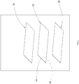
Figure 2 is a representation of a first step in the method of this disclosure. -
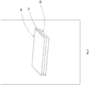
Figure 3 is a representation of a second step of the method of this disclosure. -
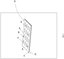
Figure 4 is a representation of a third step of the method of this disclosure. -
Figure 5 is a schematic representation of a stamp formed process used to form the phased array antenna. -
Figure 6 is a flow chart representing the method steps of this disclosure. -
Figure 1 is a schematic representation of a cross-section view of a portion of a phased array antenna embedded inside astructural panel 10 of an aircraft fabricated according to the method of this disclosure.Figure 6 is a schematic representation of a perspective view of the portion of thestructural panel 10 represented inFigure 1 . As stated earlier, thestructural panel 10 could be a panel of the fuselage construction of the aircraft, apanel 10 of a wing construction of the aircraft, apanel 10 of a tail rudder construction of the aircraft, or a panel of other structural panels of the overall aircraft construction. - Referring to
Figure 2 , in the method of constructing the antenna embedded inside astructural panel 10 of an aircraft, a first sheet offiberglass 12 is formed. To enhance the structural strength of thepanel 10, a high strength fiberglass, such as Astroquartz fiberglass produced by JPS Composite Materials, a subsidiary of JPS Industries, Inc. is used to form thefirst sheet 12. Although thefirst sheet 12 is represented as having a general rectangular configuration inFigure 2 , thefirst sheet 12 could have any configuration that would match the configuration of the structural component part of the aircraft panel constructed according to the method described herein. Additionally, although thefirst sheet 12 is represented as being generally flat inFigure 2 , thefirst sheet 12 could in most applications have a curved configuration that matches the curved configuration of the structural component part of the aircraft the panel is to become a part of. Such afirst sheet 12 constructed of fiberglass is rigid and has a curved configuration. Atop surface 14 of the first sheet has a general convex configuration and thebottom surface 16 of thefirst sheet 12 has a general concave configuration. - Referring to
Figures 1 and2 , afirst antenna layer 18 is represented. Thefirst antenna layer 18 has the same configuration as thefirst sheet 12. Thefirst antenna layer 18 is constructed of electrically conductive material that is often used in the construction of antennas, for example copper foil. - Also represented in
Figures 1 and2 is a RF powerdistribution network layer 22. Thedistribution network layer 22 has the same configuration as thefirst sheet 12. Thedistribution network layer 22 is also constructed of electrically conductive material that is often used in the construction of antennas, for example copper foil. -
Figure 3 is a representation of fixing thefirst antenna layer 18 to thetop surface 14 of thefirst sheet 12, and fixing thedistribution network layer 22 to thebottom surface 16 of thefirst sheet 12. Thefirst antenna layer 18 and thedistribution network layer 22 can be fixed to the opposite surfaces of thefirst sheet 12 according to any of the known methods and processes used in the production of a printed circuit board. - Referring to
Figure 4 , a desired antenna configuration is formed into thefirst antenna layer 18 on thefirst sheet 12, and a desired distribution network configuration is formed in thedistribution network layer 22 on thefirst sheet 12. The first antenna configuration can be formed into thefirst antenna layer 18 by any of the known methods and processes used in the production of a printed circuit board. For example, an ultraviolet light sensitive film or a photo "resist" film is applied and secured to thefirst antenna layer 18 on thefirst sheet 12 by the application of heat and pressure. An image film having the desired configuration of the first antenna layer is then applied over the "resist" film. - The
first antenna layer 18 is then exposed to high intensity ultraviolet light. The ultraviolet light passes through clear areas of the image film and hardens portions of the "resist" film that are not covered by the dark areas of the image film. - The portions of the "resist" layer that are not hardened by the ultraviolet light are then removed. This exposes portions of the first antenna layer electrically conductive material that are not covered by the hardened "resist". The exposed portions of the electrically conductive material of the first antenna layer are then removed chemically as represented by the
areas 24 inFigure 4 , thereby etching the desired first antenna configuration into the first antenna layer. The hardened "resist" is then removed, exposing the configuration of thefirst antenna layer 18 on thetop surface 14 of thefirst sheet 12. - The distribution network configuration is formed in the
distribution network layer 22 in the same manner discussed above with regard to thefirst antenna layer 18 configuration. - The above method steps produce the
first antenna layer 18, thefirst sheet 12 of fiberglass and thedistribution network layer 22 represented inFigure 5 . To create a phased array antenna inside thepanel 10 of the aircraft, asecond sheet 26 of high strength fiberglass is then formed. Thesecond sheet 26 has the same configuration as thefirst sheet 12, and is constructed in substantially the same manner. Thesecond sheet 26 is also rigid and has a curved configuration with atop surface 28 having a general convex configuration and anopposite bottom surface 32 having a general concave configuration. In substantially the same manner as thefirst antenna layer 18, asecond antenna layer 34 of electrically conductive material, for example copper foil, is fixed to thebottom surface 32 of thesecond sheet 26. In substantially the same manner as described above with regard to thefirst sheet 12, a desired second antenna configuration is etched into thesecond antenna layer 34. - Inter-laminar feeds or
vias 36 are formed throughfirst sheet 12, and thesecond sheet 26. Thevias 36 are provided to enable electric communication between thefirst antenna layer 18, thedistribution network layer 22 and thesecond antenna layer 34. - As represented in
Figure 5 , thefirst sheet 12 and thesecond sheet 26 are then registered relative to each other or are positioned relative to each other in the positions they will occupy in the final construction of the phased array antenna inside thepanel 10 of the aircraft.Electrical communicators 38 are passed throughvias 36 and communicate with thefirst antenna layer 18 and thesecond antenna layer 34, providing electrical communications between the two antenna layers. Thedistribution network layer 22 is capacitively coupled to thefirst antenna layer 18 and thesecond antenna layer 34. - With the
first antenna layer 18, thedistribution network layer 22 and thesecond antenna layer 34 connected in electrical communication by theelectrical communicators 38, thefirst sheet 12 and thesecond sheet 26 are positioned relative to each other or are registered relative to each other in a molding apparatus that is operable to perform a stamp forming process.Figure 5 is a schematic representation of a molding apparatus comprising amold 40 and apress 42. Thefirst sheet 12 and thesecond sheet 26, together with thefirst antenna layer 18, thesecond antenna layer 34, thedistribution network layer 22 all communicating through theelectrical communicators 38 are positioned in themold 40. Thepress 42 is then lowered into themold 40 applying pressure to thefirst sheet 12 and thesecond sheet 26 while themold 40 heats thefirst sheet 12 and thesecond sheet 26. Thefirst sheet 12 and thesecond sheet 26 are then secured together using the stamp forming process, for example a thermoset stamp forming process, with thetop surface 28 of thesecond sheet 26 engaging against thebottom surface 16 of thefirst sheet 12, creating a phased array antenna inside astructural panel 10 of an aircraft. - As represented in
Figure 1 , thefirst sheet 12 and thesecond sheet 26 that have been cured together can then be secured to an opencell core panel 44 of thestructural panel 10 of the aircraft. Additional structural sheets 46 (referred to herein as a "third sheet 46") are also represented inFigure 1 . These additionalstructural sheets 46 could be additional layers of fiberglass or other equivalent materials employed in the construction of thestructural panel 10, depending on the intended use of thestructural panel 10 in the aircraft. Eachthird sheet 46 includes a top surface and a bottom surface. Where thestructural panel 10 is to be used as part of an exterior structure of the aircraft, aprotective cover layer 48 could be applied to thestructural panel 10 to protect the antenna inside the panel. - Although the
structural panel 10 has been described above as having afirst antenna layer 18 and asecond antenna layer 34, thepanel 10 could be comprised of additional antenna layers and additional distribution layers. The antenna layers and the distribution layers of the antenna would all be communicated byelectrical communicators 52 that extend through thecore panel 44 and the additionalstructural sheets 46 to anelectrical connector interface 54. - Referring now to
Figure 6 , a flow chart representing the method steps of this disclosure is disclosed. Themethod 100 of embedding an antenna inside a structural panel of an aircraft includes forming 102 a first sheet from fiberglass with the first sheet being rigid and having a top surface and an opposite bottom surface. The top surface could be formed as a convex configuration with the first sheet having a bottom surface that has a concave configuration. A first antenna layer of electrically conductive material is then fixed 104 to the top surface of the first sheet. The conductive material can be, for example, copper foil. A distribution network layer of electrically conductive material can then be fixed 106 to the bottom surface of the first sheet. The conductive material can be, for example, copper foil. Themethod 100 further includes etching 108 a first antenna configuration into the first antenna layer and etching 110 a distribution network configuration into the distribution network layer. A second sheet from fiberglass is formed 112 with the second sheet being rigid and having a top surface and an opposite bottom surface. The top surface can have a convex configuration and the bottom surface can have a concave configuration. A second antenna layer of electrically conductive material is then fixed 114 to the bottom surface of the second sheet. The conductive material can be, for example, copper foil. The method further includes etching 116 a second antenna configuration into the second antenna layer and securing 118 the first sheet to the second sheet with the bottom surface of the first sheet engaging with the top surface of the second sheet. - Further, the disclosure comprises examples according to the following clauses:
- Clause 1. A method of embedding an antenna inside a structural panel of an aircraft, the method comprising:
- forming a first sheet from fiberglass with the first sheet being rigid and having a top surface and an opposite bottom surface;
- fixing a first antenna layer of electrically conductive material to the top surface of the first sheet;
- fixing a distribution network layer of electrically conductive material to the bottom surface of the first sheet;
- etching a first antenna configuration into the first antenna layer;
- etching a distribution network configuration into the distribution network layer;
- forming a second sheet from fiberglass with the second sheet being rigid and having a top surface and an opposite bottom surface;
- fixing a second antenna layer of electrically conductive material to the bottom surface of the second sheet;
- etching a second antenna configuration into the second antenna layer; and,
- securing the first sheet to the second sheet with the bottom surface of the first sheet engaging with the top surface of the second sheet.
- Clause 2. The method of Clause 1, further comprising:
securing the first sheet to the second sheet by applying heat and compression pressure to the first sheet and the second sheet in a stamp forming process. - Clause 3. The method of Clause 2, further comprising:
registering the first sheet and the second sheet relative to each other prior to applying heat and compression pressure to the first sheet and the second sheet in the stamp forming process. - Clause 4. The method of Clause 1, further comprising:
- forming the first sheet with a curved configuration; and,
- forming the second sheet with a curved configuration.
- Clause 5. The method of Clause 1, further comprising:
securing the first sheet and the second sheet to an open cell core panel of the structural panel of the aircraft. - Clause 6. The method of Clause 1, further comprising:
- forming vias through the second sheet; and,
- electrically communicating the first antenna layer and the second antenna layer through the vias formed through the second sheet.
- Clause 7. The method of Clause 1, further comprising:
forming the structural panel as a portion of a fuselage of the aircraft. - Clause 8. The method of Clause 1, further comprising:
forming the structural panel as a portion of a wing of the aircraft. - Clause 9. The method of Clause 1, further comprising:
forming the structural panel as a portion of a tail rudder of the aircraft. -
Clause 10. A method of embedding an antenna inside a structural panel of an aircraft, the method comprising:- forming a first sheet from fiberglass with the first sheet being rigid and having a curved configuration, the first sheet having a top surface that has a convex configuration and the first sheet having a bottom surface that has a concave configuration;
- fixing a first antenna layer of copper foil to the top surface of the first sheet;
- fixing a distribution network layer of copper foil to the bottom surface of the first sheet;
- etching a first antenna configuration into the first antenna layer;
- etching a distribution network configuration into the distribution network layer;
- forming a second sheet from fiberglass with the second sheet being rigid and having a curved configuration, the second sheet having a top surface that has a convex configuration and the second sheet having a bottom surface that has a concave configuration;
- fixing a second antenna layer of copper foil to the bottom surface of the second sheet;
- etching a second antenna configuration into the second antenna layer; and,
securing the first sheet to the second sheet with the top surface of the second sheet engaging against the bottom surface of the first sheet.
- Clause 11. The method of
Clause 10, further comprising:
creating a phased array antenna by securing the first sheet to the second sheet. -
Clause 12. The method of Clause 11, further comprising:- forming vias through the second sheet;
- electrically communicating the first antenna layer and the second antenna layer through the vias formed through the second sheet prior to securing the first sheet to the second sheet; and,
- applying heat and compression pressure to the first sheet and the second sheet when securing the first sheet to the second sheet using the stamp forming process.
- Clause 13. The method of
Clause 10, further comprising:
after securing the first sheet to the second sheet using a stamp forming process, securing the first sheet and the second sheet to an open cell core panel of the structural panel of the aircraft. -
Clause 14. The method ofClause 10, further comprising:- forming a third sheet from fiberglass with the third sheet being rigid and having a curved configuration, the third sheet having a top surface that has a convex configuration and the third sheet having a bottom surface that has a concave configuration; and,
- securing the third sheet to the second sheet using the stamped forming process with the top surface of the third sheet engaging against the second antenna layer of copper foil fixed to the bottom surface of the second sheet.
- Clause 15. The method of
Clause 14, further comprising:
forming the structural panel as a portion of a fuselage of the aircraft. -
Clause 16. The method ofClause 14, further comprising:
forming the structural panel as a portion of a wing of the aircraft. - Clause 17. The method of
Clause 14, further comprising:
forming the structural panel as a portion of a tail rudder of the aircraft. -
Clause 18. A structural panel of an aircraft having an embedded antenna, the structural panel comprising:- a first sheet of fiberglass, the first sheet being rigid and having a top surface and an opposite bottom surface;
- a first antenna layer fixed on the top surface of the first sheet;
- a distribution network layer fixed on the bottom surface of the first sheet;
- a second sheet of fiberglass, the second sheet being rigid and having a top surface and an opposite bottom surface;
- a second antenna layer fixed on the bottom surface of the second sheet; and,
- the first sheet and the second sheet having been secured together with the bottom surface of the first sheet engaging with the top surface of the second sheet. Clause 19. The structural panel of
Clause 18, further comprising:- a third sheet of fiberglass, the third sheet being rigid and having a top surface and an opposite bottom surface;
- a second antenna layer secured to the bottom surface of the third sheet; and,
- the third sheet being secured to the first sheet and the second sheet by the stamp forming process with the bottom surface of the second sheet engaging with the top surface of the third sheet.
- Clause 20. The structural panel of Clause 19, further comprising:
the structural panel being on a portion of an exterior surface of the aircraft. - As various modifications could be made in the method of constructing the structural panel of an aircraft with an embedded antenna and the panel herein described and illustrated without departing from the scope of the invention, it is intended that all matter contained in the foregoing description or shown in the accompanying drawings shall be interpreted as illustrative rather than limiting. Thus, the breadth and scope of the present disclosure should not be limited by any of the above described exemplary examples, but should be defined only in accordance with the following claims appended hereto and their equivalents.
Claims (15)
- A method (100) of embedding an antenna inside a structural panel (10) of an aircraft, the method comprising:forming (102) a first sheet (12) from fiberglass with the first sheet (12) being rigid and having a top surface (14) and an opposite bottom surface (16);fixing (104) a first antenna layer (18) of electrically conductive material to the top surface of the first sheet (12);fixing (106) a distribution network layer (22) of electrically conductive material to the bottom surface (16) of the first sheet (12);etching (108) a first antenna configuration into the first antenna layer (18);etching (110) a distribution network configuration into the distribution network layer (22);forming (112) a second sheet (26) from fiberglass with the second sheet (26) being rigid and having a top surface (28) and an opposite bottom surface (32);fixing (114) a second antenna layer (34) of electrically conductive material to the bottom surface of the second sheet (26);etching (116) a second antenna configuration into the second antenna layer (34); andsecuring (118) the first sheet (12) to the second sheet (26) with the bottom surface (16) of the first sheet (12) engaging with the top surface (28) of the second sheet (26).
- The method of claim 1, further comprising:securing the first sheet (12) to the second sheet (26) by applying heat and compression pressure to the first sheet (12) and the second sheet (26) in a stamp forming process.
- The method of claim 2, further comprising:registering the first sheet (12) and the second sheet (26) relative to each other prior to applying heat and compression pressure to the first sheet (12) and the second sheet (26) in the stamp forming process.
- The method of any one of claims 1-3, further comprising:securing the first sheet (12) and the second sheet (26) to an open cell core panel (44) of the structural panel (10) of the aircraft.
- The method of any one of claims 1-4, further comprising:forming vias (36) through the second sheet; and,electrically communicating the first antenna layer (18) and the second antenna layer (34) through the vias (36)formed through the second sheet (26).
- The method of any one of claims 1-5, further comprising:forming the structural panel (10) as a portion of a fuselage of the aircraft.
- The method of any one of claims 1-6, further comprising:forming the structural panel (10) as a portion of a wing of the aircraft.
- The method of any one of claims 1-7, further comprising:forming the structural panel (10) as a portion of a tail rudder of the aircraft.
- The method (100) of claim 1 wherein:the first sheet (12) has a curved configuration, the top surface (14) having a convex configuration and the bottom surface (16) having a concave configuration;the electrically conductive layer of the first antenna layer (18) and the distribution network layer (22) comprise copper foil, and whereinthe second sheet (26) has a curved configuration, the top surface (28) having a convex configuration and the bottom surface (32) having a concave configuration;and wherein the second antenna layer (34) comprises copper foil.
- The method of claim 9, further comprising:forming vias (36) through the second sheet (26);electrically communicating the first antenna layer (18) and the second antenna layer (34) through the vias (36) formed through the second sheet (26) prior to securing the first sheet (12) to the second sheet (26); and,applying heat and compression pressure to the first sheet (12) and the second sheet (26) when securing the first sheet (12) to the second sheet using a stamp forming process.
- The method of claim 10, further comprising:after securing the first sheet (12) to the second sheet (26) using a stamp forming process, securing the first sheet (12) and the second sheet (26) to an open cell core panel (44) of the structural panel (10) of the aircraft.
- The method of any one of claims 9-11, further comprising:forming a third sheet (46) from fiberglass with the third sheet being rigid and having a curved configuration, the third sheet (46) having a top surface that has a convex configuration and the third sheet (46) having a bottom surface that has a concave configuration; andsecuring the third sheet (46) to the second sheet (26) using the stamped forming process with the top surface of the third sheet (46) engaging against the second antenna layer (34) of copper foil fixed to the bottom surface of the second sheet (26).
- A structural panel (10) of an aircraft having an embedded antenna, the structural panel (10) comprising:a first sheet (12) of fiberglass, the first sheet (12) being rigid and having a top surface (14) and an opposite bottom surface (16);a first antenna layer (18) fixed on the top surface (14) of the first sheet (12);a distribution network layer (22) fixed on the bottom surface (16)of the first sheet (12);a second sheet (26) of fiberglass, the second sheet (26) being rigid and having a top surface (28) and an opposite bottom surface (32);a second antenna layer (34) fixed on the bottom surface of the second sheet (26); andthe first sheet (12) and the second sheet (26) having been secured together with the bottom surface (16) of the first sheet (12) engaging with the top surface (28) of the second sheet (26).
- The structural panel (10) of claim 13, further comprising:a third sheet (46) of fiberglass, the third sheet (46) being rigid and having a top surface and an opposite bottom surface;a second antenna layer (34) secured to the bottom surface of the third sheet; and,the third sheet (46) being secured to the first sheet (12) and the second sheet (26) by a stamp forming process with the bottom surface (28) of the second sheet (26) engaging with the top surface of the third sheet.
- The structural panel (10) of claim 13 or 14, further comprising:the structural panel (10) being on a portion of an exterior surface of the aircraft.
Applications Claiming Priority (1)
| Application Number | Priority Date | Filing Date | Title |
|---|---|---|---|
| US15/671,796 US10340584B2 (en) | 2017-08-08 | 2017-08-08 | Structural multilayer antenna design and fabrication |
Publications (2)
| Publication Number | Publication Date |
|---|---|
| EP3442078A1 true EP3442078A1 (en) | 2019-02-13 |
| EP3442078B1 EP3442078B1 (en) | 2023-05-03 |
Family
ID=63244381
Family Applications (1)
| Application Number | Title | Priority Date | Filing Date |
|---|---|---|---|
| EP18186238.4A Active EP3442078B1 (en) | 2017-08-08 | 2018-07-30 | Structural multilayer antenna design and fabrication |
Country Status (5)
| Country | Link |
|---|---|
| US (1) | US10340584B2 (en) |
| EP (1) | EP3442078B1 (en) |
| JP (1) | JP7214387B2 (en) |
| CN (1) | CN109390681B (en) |
| CA (1) | CA3006195C (en) |
Families Citing this family (1)
| Publication number | Priority date | Publication date | Assignee | Title |
|---|---|---|---|---|
| CN115835484B (en) * | 2022-12-30 | 2026-04-28 | 维沃移动通信有限公司 | Circuit boards and electronic equipment |
Citations (5)
| Publication number | Priority date | Publication date | Assignee | Title |
|---|---|---|---|---|
| US4208660A (en) * | 1977-11-11 | 1980-06-17 | Raytheon Company | Radio frequency ring-shaped slot antenna |
| US5184141A (en) * | 1990-04-05 | 1993-02-02 | Vought Aircraft Company | Structurally-embedded electronics assembly |
| US5437091A (en) * | 1993-06-28 | 1995-08-01 | Honeywell Inc. | High curvature antenna forming process |
| US5648786A (en) * | 1995-11-27 | 1997-07-15 | Trw Inc. | Conformal low profile wide band slot phased array antenna |
| US7167129B1 (en) * | 2004-10-12 | 2007-01-23 | Sandia Corporation | Reproducible, high performance patch antenna array apparatus and method of fabrication |
Family Cites Families (15)
| Publication number | Priority date | Publication date | Assignee | Title |
|---|---|---|---|---|
| US3623162A (en) * | 1970-07-24 | 1971-11-23 | Sanders Associates Inc | Folded slot antenna |
| JPH0833242A (en) * | 1994-07-18 | 1996-02-02 | Nissan Motor Co Ltd | Microwave power transmission / reception device and mounting method thereof |
| US7342801B2 (en) * | 2004-04-29 | 2008-03-11 | Harris Corporation | Printed wiring board with enhanced structural integrity |
| US7518555B2 (en) * | 2005-08-04 | 2009-04-14 | Amphenol Corporation | Multi-band antenna structure |
| JP4912716B2 (en) * | 2006-03-29 | 2012-04-11 | 新光電気工業株式会社 | Wiring substrate manufacturing method and semiconductor device manufacturing method |
| US7883050B2 (en) | 2007-06-28 | 2011-02-08 | The Boeing Company | Composites with integrated multi-functional circuits |
| CN201114997Y (en) * | 2007-07-23 | 2008-09-10 | 苏州欧西亚电子科技有限公司 | Built-in antenna device |
| JP5701737B2 (en) | 2011-12-20 | 2015-04-15 | 株式会社東芝 | Antenna device |
| US9325058B2 (en) * | 2012-07-18 | 2016-04-26 | Intel Corporation | Broadband aircraft wingtip antenna system |
| TWI539675B (en) * | 2013-12-26 | 2016-06-21 | Chunghwa Telecom Co Ltd | Dual Directional Multiple Input Multiple Output Antenna Units and Their Arrays |
| TWI568081B (en) * | 2014-11-05 | 2017-01-21 | 晶越微波積體電路製造股份有限公司 | Antenna apparatus and wireless communication system using the same |
| US9360696B1 (en) * | 2014-12-11 | 2016-06-07 | Amazon Technologies, Inc. | Electronic device stack assembly |
| US10199745B2 (en) * | 2015-06-04 | 2019-02-05 | The Boeing Company | Omnidirectional antenna system |
| JP6591909B2 (en) * | 2015-07-27 | 2019-10-16 | 京セラ株式会社 | Antenna module |
| CN105914455B (en) * | 2016-04-13 | 2019-07-23 | 深圳中科系统集成技术有限公司 | A kind of miniaturization NFC antenna and mobile terminal |
-
2017
- 2017-08-08 US US15/671,796 patent/US10340584B2/en active Active
-
2018
- 2018-05-24 CA CA3006195A patent/CA3006195C/en active Active
- 2018-07-09 CN CN201810743467.3A patent/CN109390681B/en active Active
- 2018-07-20 JP JP2018136610A patent/JP7214387B2/en active Active
- 2018-07-30 EP EP18186238.4A patent/EP3442078B1/en active Active
Patent Citations (5)
| Publication number | Priority date | Publication date | Assignee | Title |
|---|---|---|---|---|
| US4208660A (en) * | 1977-11-11 | 1980-06-17 | Raytheon Company | Radio frequency ring-shaped slot antenna |
| US5184141A (en) * | 1990-04-05 | 1993-02-02 | Vought Aircraft Company | Structurally-embedded electronics assembly |
| US5437091A (en) * | 1993-06-28 | 1995-08-01 | Honeywell Inc. | High curvature antenna forming process |
| US5648786A (en) * | 1995-11-27 | 1997-07-15 | Trw Inc. | Conformal low profile wide band slot phased array antenna |
| US7167129B1 (en) * | 2004-10-12 | 2007-01-23 | Sandia Corporation | Reproducible, high performance patch antenna array apparatus and method of fabrication |
Also Published As
| Publication number | Publication date |
|---|---|
| EP3442078B1 (en) | 2023-05-03 |
| CA3006195A1 (en) | 2019-02-08 |
| JP2019081532A (en) | 2019-05-30 |
| CN109390681B (en) | 2022-11-25 |
| CN109390681A (en) | 2019-02-26 |
| US20190051976A1 (en) | 2019-02-14 |
| JP7214387B2 (en) | 2023-01-30 |
| US10340584B2 (en) | 2019-07-02 |
| CA3006195C (en) | 2022-09-20 |
Similar Documents
| Publication | Publication Date | Title |
|---|---|---|
| KR102524713B1 (en) | Omnidirectional antenna system | |
| US7523545B2 (en) | Methods of manufacturing printed circuit boards with stacked micro vias | |
| US6496151B1 (en) | End-fire cavity slot antenna array structure and method of forming | |
| CA2921097C (en) | Conformal composite antenna assembly | |
| US7829796B2 (en) | Circuit joining assembly materials for multi-layer lightning protection systems on composite aircraft | |
| US11276933B2 (en) | High-gain antenna with cavity between feed line and ground plane | |
| KR101772088B1 (en) | Method for designing electromagnetic properties using multi-layered stack with electromagnetic material printing | |
| Beziuk et al. | Electromagnetic and electronic aerospace conformal load-bearing smart skins: A review | |
| CA3006195C (en) | Structural multilayer antenna design and fabrication | |
| CN110718741A (en) | Bearable sandwich structure of integrated antenna array | |
| Ribeiro Filho et al. | A telemetry antenna design for a sounding rocket competition [antenna applications corner] | |
| CN111923562A (en) | Laminating process of white epoxy glass fiber cloth laminated board | |
| US20200395672A1 (en) | Antenna assembly having one or more cavities | |
| CN111864408B (en) | A vehicle-mounted millimeter wave radar array antenna | |
| CN120380888B (en) | Forming method of double-layer honeycomb sandwich antenna board | |
| GB2545655A (en) | A structure formed from composite material | |
| Avireni et al. | Conductive Fabric-Based Embedded Antenna Structures for Automotive Applications | |
| Ghorbani et al. | Advances aerospace multifunctional structures with integrated antenna structures | |
| EP4620056A1 (en) | Radome-enclosure | |
| US20140037889A1 (en) | Insulator for build-up pcb and method of manufacturing pcb using the same | |
| CN116207508A (en) | Multi-interlayer composite material for frequency selective surface, preparation method and phased array radar radome |
Legal Events
| Date | Code | Title | Description |
|---|---|---|---|
| PUAI | Public reference made under article 153(3) epc to a published international application that has entered the european phase |
Free format text: ORIGINAL CODE: 0009012 |
|
| STAA | Information on the status of an ep patent application or granted ep patent |
Free format text: STATUS: REQUEST FOR EXAMINATION WAS MADE |
|
| 17P | Request for examination filed |
Effective date: 20180730 |
|
| AK | Designated contracting states |
Kind code of ref document: A1 Designated state(s): AL AT BE BG CH CY CZ DE DK EE ES FI FR GB GR HR HU IE IS IT LI LT LU LV MC MK MT NL NO PL PT RO RS SE SI SK SM TR |
|
| AX | Request for extension of the european patent |
Extension state: BA ME |
|
| RBV | Designated contracting states (corrected) |
Designated state(s): AL AT BE BG CH CY CZ DE DK EE ES FI FR GB GR HR HU IE IS IT LI LT LU LV MC MK MT NL NO PL PT RO RS SE SI SK SM TR |
|
| STAA | Information on the status of an ep patent application or granted ep patent |
Free format text: STATUS: EXAMINATION IS IN PROGRESS |
|
| 17Q | First examination report despatched |
Effective date: 20210224 |
|
| GRAP | Despatch of communication of intention to grant a patent |
Free format text: ORIGINAL CODE: EPIDOSNIGR1 |
|
| STAA | Information on the status of an ep patent application or granted ep patent |
Free format text: STATUS: GRANT OF PATENT IS INTENDED |
|
| INTG | Intention to grant announced |
Effective date: 20220708 |
|
| GRAJ | Information related to disapproval of communication of intention to grant by the applicant or resumption of examination proceedings by the epo deleted |
Free format text: ORIGINAL CODE: EPIDOSDIGR1 |
|
| STAA | Information on the status of an ep patent application or granted ep patent |
Free format text: STATUS: EXAMINATION IS IN PROGRESS |
|
| GRAP | Despatch of communication of intention to grant a patent |
Free format text: ORIGINAL CODE: EPIDOSNIGR1 |
|
| INTC | Intention to grant announced (deleted) | ||
| STAA | Information on the status of an ep patent application or granted ep patent |
Free format text: STATUS: GRANT OF PATENT IS INTENDED |
|
| INTG | Intention to grant announced |
Effective date: 20221124 |
|
| GRAS | Grant fee paid |
Free format text: ORIGINAL CODE: EPIDOSNIGR3 |
|
| RAP3 | Party data changed (applicant data changed or rights of an application transferred) |
Owner name: THE BOEING COMPANY |
|
| GRAA | (expected) grant |
Free format text: ORIGINAL CODE: 0009210 |
|
| STAA | Information on the status of an ep patent application or granted ep patent |
Free format text: STATUS: THE PATENT HAS BEEN GRANTED |
|
| AK | Designated contracting states |
Kind code of ref document: B1 Designated state(s): AL AT BE BG CH CY CZ DE DK EE ES FI FR GB GR HR HU IE IS IT LI LT LU LV MC MK MT NL NO PL PT RO RS SE SI SK SM TR |
|
| REG | Reference to a national code |
Ref country code: GB Ref legal event code: FG4D |
|
| REG | Reference to a national code |
Ref country code: AT Ref legal event code: REF Ref document number: 1565472 Country of ref document: AT Kind code of ref document: T Effective date: 20230515 Ref country code: CH Ref legal event code: EP |
|
| REG | Reference to a national code |
Ref country code: DE Ref legal event code: R096 Ref document number: 602018049120 Country of ref document: DE |
|
| REG | Reference to a national code |
Ref country code: IE Ref legal event code: FG4D |
|
| P01 | Opt-out of the competence of the unified patent court (upc) registered |
Effective date: 20230526 |
|
| REG | Reference to a national code |
Ref country code: LT Ref legal event code: MG9D |
|
| REG | Reference to a national code |
Ref country code: NL Ref legal event code: MP Effective date: 20230503 |
|
| REG | Reference to a national code |
Ref country code: AT Ref legal event code: MK05 Ref document number: 1565472 Country of ref document: AT Kind code of ref document: T Effective date: 20230503 |
|
| PG25 | Lapsed in a contracting state [announced via postgrant information from national office to epo] |
Ref country code: SE Free format text: LAPSE BECAUSE OF FAILURE TO SUBMIT A TRANSLATION OF THE DESCRIPTION OR TO PAY THE FEE WITHIN THE PRESCRIBED TIME-LIMIT Effective date: 20230503 Ref country code: PT Free format text: LAPSE BECAUSE OF FAILURE TO SUBMIT A TRANSLATION OF THE DESCRIPTION OR TO PAY THE FEE WITHIN THE PRESCRIBED TIME-LIMIT Effective date: 20230904 Ref country code: NO Free format text: LAPSE BECAUSE OF FAILURE TO SUBMIT A TRANSLATION OF THE DESCRIPTION OR TO PAY THE FEE WITHIN THE PRESCRIBED TIME-LIMIT Effective date: 20230803 Ref country code: NL Free format text: LAPSE BECAUSE OF FAILURE TO SUBMIT A TRANSLATION OF THE DESCRIPTION OR TO PAY THE FEE WITHIN THE PRESCRIBED TIME-LIMIT Effective date: 20230503 Ref country code: ES Free format text: LAPSE BECAUSE OF FAILURE TO SUBMIT A TRANSLATION OF THE DESCRIPTION OR TO PAY THE FEE WITHIN THE PRESCRIBED TIME-LIMIT Effective date: 20230503 Ref country code: AT Free format text: LAPSE BECAUSE OF FAILURE TO SUBMIT A TRANSLATION OF THE DESCRIPTION OR TO PAY THE FEE WITHIN THE PRESCRIBED TIME-LIMIT Effective date: 20230503 |
|
| PG25 | Lapsed in a contracting state [announced via postgrant information from national office to epo] |
Ref country code: RS Free format text: LAPSE BECAUSE OF FAILURE TO SUBMIT A TRANSLATION OF THE DESCRIPTION OR TO PAY THE FEE WITHIN THE PRESCRIBED TIME-LIMIT Effective date: 20230503 Ref country code: PL Free format text: LAPSE BECAUSE OF FAILURE TO SUBMIT A TRANSLATION OF THE DESCRIPTION OR TO PAY THE FEE WITHIN THE PRESCRIBED TIME-LIMIT Effective date: 20230503 Ref country code: LV Free format text: LAPSE BECAUSE OF FAILURE TO SUBMIT A TRANSLATION OF THE DESCRIPTION OR TO PAY THE FEE WITHIN THE PRESCRIBED TIME-LIMIT Effective date: 20230503 Ref country code: LT Free format text: LAPSE BECAUSE OF FAILURE TO SUBMIT A TRANSLATION OF THE DESCRIPTION OR TO PAY THE FEE WITHIN THE PRESCRIBED TIME-LIMIT Effective date: 20230503 Ref country code: IS Free format text: LAPSE BECAUSE OF FAILURE TO SUBMIT A TRANSLATION OF THE DESCRIPTION OR TO PAY THE FEE WITHIN THE PRESCRIBED TIME-LIMIT Effective date: 20230903 Ref country code: HR Free format text: LAPSE BECAUSE OF FAILURE TO SUBMIT A TRANSLATION OF THE DESCRIPTION OR TO PAY THE FEE WITHIN THE PRESCRIBED TIME-LIMIT Effective date: 20230503 Ref country code: GR Free format text: LAPSE BECAUSE OF FAILURE TO SUBMIT A TRANSLATION OF THE DESCRIPTION OR TO PAY THE FEE WITHIN THE PRESCRIBED TIME-LIMIT Effective date: 20230804 |
|
| PG25 | Lapsed in a contracting state [announced via postgrant information from national office to epo] |
Ref country code: FI Free format text: LAPSE BECAUSE OF FAILURE TO SUBMIT A TRANSLATION OF THE DESCRIPTION OR TO PAY THE FEE WITHIN THE PRESCRIBED TIME-LIMIT Effective date: 20230503 |
|
| PG25 | Lapsed in a contracting state [announced via postgrant information from national office to epo] |
Ref country code: SK Free format text: LAPSE BECAUSE OF FAILURE TO SUBMIT A TRANSLATION OF THE DESCRIPTION OR TO PAY THE FEE WITHIN THE PRESCRIBED TIME-LIMIT Effective date: 20230503 |
|
| PG25 | Lapsed in a contracting state [announced via postgrant information from national office to epo] |
Ref country code: SM Free format text: LAPSE BECAUSE OF FAILURE TO SUBMIT A TRANSLATION OF THE DESCRIPTION OR TO PAY THE FEE WITHIN THE PRESCRIBED TIME-LIMIT Effective date: 20230503 Ref country code: SK Free format text: LAPSE BECAUSE OF FAILURE TO SUBMIT A TRANSLATION OF THE DESCRIPTION OR TO PAY THE FEE WITHIN THE PRESCRIBED TIME-LIMIT Effective date: 20230503 Ref country code: RO Free format text: LAPSE BECAUSE OF FAILURE TO SUBMIT A TRANSLATION OF THE DESCRIPTION OR TO PAY THE FEE WITHIN THE PRESCRIBED TIME-LIMIT Effective date: 20230503 Ref country code: EE Free format text: LAPSE BECAUSE OF FAILURE TO SUBMIT A TRANSLATION OF THE DESCRIPTION OR TO PAY THE FEE WITHIN THE PRESCRIBED TIME-LIMIT Effective date: 20230503 Ref country code: DK Free format text: LAPSE BECAUSE OF FAILURE TO SUBMIT A TRANSLATION OF THE DESCRIPTION OR TO PAY THE FEE WITHIN THE PRESCRIBED TIME-LIMIT Effective date: 20230503 Ref country code: CZ Free format text: LAPSE BECAUSE OF FAILURE TO SUBMIT A TRANSLATION OF THE DESCRIPTION OR TO PAY THE FEE WITHIN THE PRESCRIBED TIME-LIMIT Effective date: 20230503 |
|
| REG | Reference to a national code |
Ref country code: DE Ref legal event code: R097 Ref document number: 602018049120 Country of ref document: DE |
|
| PG25 | Lapsed in a contracting state [announced via postgrant information from national office to epo] |
Ref country code: MC Free format text: LAPSE BECAUSE OF FAILURE TO SUBMIT A TRANSLATION OF THE DESCRIPTION OR TO PAY THE FEE WITHIN THE PRESCRIBED TIME-LIMIT Effective date: 20230503 |
|
| PG25 | Lapsed in a contracting state [announced via postgrant information from national office to epo] |
Ref country code: MC Free format text: LAPSE BECAUSE OF FAILURE TO SUBMIT A TRANSLATION OF THE DESCRIPTION OR TO PAY THE FEE WITHIN THE PRESCRIBED TIME-LIMIT Effective date: 20230503 |
|
| REG | Reference to a national code |
Ref country code: CH Ref legal event code: PL |
|
| PLBE | No opposition filed within time limit |
Free format text: ORIGINAL CODE: 0009261 |
|
| STAA | Information on the status of an ep patent application or granted ep patent |
Free format text: STATUS: NO OPPOSITION FILED WITHIN TIME LIMIT |
|
| REG | Reference to a national code |
Ref country code: BE Ref legal event code: MM Effective date: 20230731 |
|
| PG25 | Lapsed in a contracting state [announced via postgrant information from national office to epo] |
Ref country code: LU Free format text: LAPSE BECAUSE OF NON-PAYMENT OF DUE FEES Effective date: 20230730 |
|
| PG25 | Lapsed in a contracting state [announced via postgrant information from national office to epo] |
Ref country code: LU Free format text: LAPSE BECAUSE OF NON-PAYMENT OF DUE FEES Effective date: 20230730 |
|
| 26N | No opposition filed |
Effective date: 20240206 |
|
| REG | Reference to a national code |
Ref country code: IE Ref legal event code: MM4A |
|
| PG25 | Lapsed in a contracting state [announced via postgrant information from national office to epo] |
Ref country code: CH Free format text: LAPSE BECAUSE OF NON-PAYMENT OF DUE FEES Effective date: 20230731 |
|
| PG25 | Lapsed in a contracting state [announced via postgrant information from national office to epo] |
Ref country code: SI Free format text: LAPSE BECAUSE OF FAILURE TO SUBMIT A TRANSLATION OF THE DESCRIPTION OR TO PAY THE FEE WITHIN THE PRESCRIBED TIME-LIMIT Effective date: 20230503 |
|
| PG25 | Lapsed in a contracting state [announced via postgrant information from national office to epo] |
Ref country code: SI Free format text: LAPSE BECAUSE OF FAILURE TO SUBMIT A TRANSLATION OF THE DESCRIPTION OR TO PAY THE FEE WITHIN THE PRESCRIBED TIME-LIMIT Effective date: 20230503 Ref country code: IT Free format text: LAPSE BECAUSE OF FAILURE TO SUBMIT A TRANSLATION OF THE DESCRIPTION OR TO PAY THE FEE WITHIN THE PRESCRIBED TIME-LIMIT Effective date: 20230503 Ref country code: BE Free format text: LAPSE BECAUSE OF NON-PAYMENT OF DUE FEES Effective date: 20230731 |
|
| PG25 | Lapsed in a contracting state [announced via postgrant information from national office to epo] |
Ref country code: IE Free format text: LAPSE BECAUSE OF NON-PAYMENT OF DUE FEES Effective date: 20230730 |
|
| PG25 | Lapsed in a contracting state [announced via postgrant information from national office to epo] |
Ref country code: IE Free format text: LAPSE BECAUSE OF NON-PAYMENT OF DUE FEES Effective date: 20230730 |
|
| PG25 | Lapsed in a contracting state [announced via postgrant information from national office to epo] |
Ref country code: BG Free format text: LAPSE BECAUSE OF FAILURE TO SUBMIT A TRANSLATION OF THE DESCRIPTION OR TO PAY THE FEE WITHIN THE PRESCRIBED TIME-LIMIT Effective date: 20230503 |
|
| PG25 | Lapsed in a contracting state [announced via postgrant information from national office to epo] |
Ref country code: BG Free format text: LAPSE BECAUSE OF FAILURE TO SUBMIT A TRANSLATION OF THE DESCRIPTION OR TO PAY THE FEE WITHIN THE PRESCRIBED TIME-LIMIT Effective date: 20230503 |
|
| PG25 | Lapsed in a contracting state [announced via postgrant information from national office to epo] |
Ref country code: CY Free format text: LAPSE BECAUSE OF FAILURE TO SUBMIT A TRANSLATION OF THE DESCRIPTION OR TO PAY THE FEE WITHIN THE PRESCRIBED TIME-LIMIT; INVALID AB INITIO Effective date: 20180730 |
|
| PG25 | Lapsed in a contracting state [announced via postgrant information from national office to epo] |
Ref country code: HU Free format text: LAPSE BECAUSE OF FAILURE TO SUBMIT A TRANSLATION OF THE DESCRIPTION OR TO PAY THE FEE WITHIN THE PRESCRIBED TIME-LIMIT; INVALID AB INITIO Effective date: 20180730 |
|
| PGFP | Annual fee paid to national office [announced via postgrant information from national office to epo] |
Ref country code: DE Payment date: 20250729 Year of fee payment: 8 |
|
| PGFP | Annual fee paid to national office [announced via postgrant information from national office to epo] |
Ref country code: GB Payment date: 20250728 Year of fee payment: 8 |
|
| PGFP | Annual fee paid to national office [announced via postgrant information from national office to epo] |
Ref country code: FR Payment date: 20250728 Year of fee payment: 8 |
|
| PG25 | Lapsed in a contracting state [announced via postgrant information from national office to epo] |
Ref country code: TR Free format text: LAPSE BECAUSE OF FAILURE TO SUBMIT A TRANSLATION OF THE DESCRIPTION OR TO PAY THE FEE WITHIN THE PRESCRIBED TIME-LIMIT Effective date: 20230503 |