EP3441855A1 - Capacitive sensor - Google Patents
Capacitive sensor Download PDFInfo
- Publication number
- EP3441855A1 EP3441855A1 EP17778900.5A EP17778900A EP3441855A1 EP 3441855 A1 EP3441855 A1 EP 3441855A1 EP 17778900 A EP17778900 A EP 17778900A EP 3441855 A1 EP3441855 A1 EP 3441855A1
- Authority
- EP
- European Patent Office
- Prior art keywords
- panel
- adhesive layer
- intermediate layer
- base material
- layer
- Prior art date
- Legal status (The legal status is an assumption and is not a legal conclusion. Google has not performed a legal analysis and makes no representation as to the accuracy of the status listed.)
- Withdrawn
Links
Images




Classifications
-
- B—PERFORMING OPERATIONS; TRANSPORTING
- B32—LAYERED PRODUCTS
- B32B—LAYERED PRODUCTS, i.e. PRODUCTS BUILT-UP OF STRATA OF FLAT OR NON-FLAT, e.g. CELLULAR OR HONEYCOMB, FORM
- B32B27/00—Layered products comprising a layer of synthetic resin
- B32B27/06—Layered products comprising a layer of synthetic resin as the main or only constituent of a layer, which is next to another layer of the same or of a different material
- B32B27/08—Layered products comprising a layer of synthetic resin as the main or only constituent of a layer, which is next to another layer of the same or of a different material of synthetic resin
-
- B—PERFORMING OPERATIONS; TRANSPORTING
- B32—LAYERED PRODUCTS
- B32B—LAYERED PRODUCTS, i.e. PRODUCTS BUILT-UP OF STRATA OF FLAT OR NON-FLAT, e.g. CELLULAR OR HONEYCOMB, FORM
- B32B27/00—Layered products comprising a layer of synthetic resin
- B32B27/36—Layered products comprising a layer of synthetic resin comprising polyesters
- B32B27/365—Layered products comprising a layer of synthetic resin comprising polyesters comprising polycarbonates
-
- B—PERFORMING OPERATIONS; TRANSPORTING
- B32—LAYERED PRODUCTS
- B32B—LAYERED PRODUCTS, i.e. PRODUCTS BUILT-UP OF STRATA OF FLAT OR NON-FLAT, e.g. CELLULAR OR HONEYCOMB, FORM
- B32B7/00—Layered products characterised by the relation between layers; Layered products characterised by the relative orientation of features between layers, or by the relative values of a measurable parameter between layers, i.e. products comprising layers having different physical, chemical or physicochemical properties; Layered products characterised by the interconnection of layers
- B32B7/02—Physical, chemical or physicochemical properties
-
- B—PERFORMING OPERATIONS; TRANSPORTING
- B32—LAYERED PRODUCTS
- B32B—LAYERED PRODUCTS, i.e. PRODUCTS BUILT-UP OF STRATA OF FLAT OR NON-FLAT, e.g. CELLULAR OR HONEYCOMB, FORM
- B32B7/00—Layered products characterised by the relation between layers; Layered products characterised by the relative orientation of features between layers, or by the relative values of a measurable parameter between layers, i.e. products comprising layers having different physical, chemical or physicochemical properties; Layered products characterised by the interconnection of layers
- B32B7/04—Interconnection of layers
- B32B7/12—Interconnection of layers using interposed adhesives or interposed materials with bonding properties
-
- G—PHYSICS
- G06—COMPUTING OR CALCULATING; COUNTING
- G06F—ELECTRIC DIGITAL DATA PROCESSING
- G06F3/00—Input arrangements for transferring data to be processed into a form capable of being handled by the computer; Output arrangements for transferring data from processing unit to output unit, e.g. interface arrangements
- G06F3/01—Input arrangements or combined input and output arrangements for interaction between user and computer
- G06F3/03—Arrangements for converting the position or the displacement of a member into a coded form
- G06F3/041—Digitisers, e.g. for touch screens or touch pads, characterised by the transducing means
-
- G—PHYSICS
- G06—COMPUTING OR CALCULATING; COUNTING
- G06F—ELECTRIC DIGITAL DATA PROCESSING
- G06F3/00—Input arrangements for transferring data to be processed into a form capable of being handled by the computer; Output arrangements for transferring data from processing unit to output unit, e.g. interface arrangements
- G06F3/01—Input arrangements or combined input and output arrangements for interaction between user and computer
- G06F3/03—Arrangements for converting the position or the displacement of a member into a coded form
- G06F3/041—Digitisers, e.g. for touch screens or touch pads, characterised by the transducing means
- G06F3/044—Digitisers, e.g. for touch screens or touch pads, characterised by the transducing means by capacitive means
-
- G—PHYSICS
- G06—COMPUTING OR CALCULATING; COUNTING
- G06F—ELECTRIC DIGITAL DATA PROCESSING
- G06F3/00—Input arrangements for transferring data to be processed into a form capable of being handled by the computer; Output arrangements for transferring data from processing unit to output unit, e.g. interface arrangements
- G06F3/01—Input arrangements or combined input and output arrangements for interaction between user and computer
- G06F3/03—Arrangements for converting the position or the displacement of a member into a coded form
- G06F3/041—Digitisers, e.g. for touch screens or touch pads, characterised by the transducing means
- G06F3/044—Digitisers, e.g. for touch screens or touch pads, characterised by the transducing means by capacitive means
- G06F3/0443—Digitisers, e.g. for touch screens or touch pads, characterised by the transducing means by capacitive means using a single layer of sensing electrodes
-
- G—PHYSICS
- G06—COMPUTING OR CALCULATING; COUNTING
- G06F—ELECTRIC DIGITAL DATA PROCESSING
- G06F3/00—Input arrangements for transferring data to be processed into a form capable of being handled by the computer; Output arrangements for transferring data from processing unit to output unit, e.g. interface arrangements
- G06F3/01—Input arrangements or combined input and output arrangements for interaction between user and computer
- G06F3/03—Arrangements for converting the position or the displacement of a member into a coded form
- G06F3/041—Digitisers, e.g. for touch screens or touch pads, characterised by the transducing means
- G06F3/044—Digitisers, e.g. for touch screens or touch pads, characterised by the transducing means by capacitive means
- G06F3/0446—Digitisers, e.g. for touch screens or touch pads, characterised by the transducing means by capacitive means using a grid-like structure of electrodes in at least two directions, e.g. using row and column electrodes
-
- B—PERFORMING OPERATIONS; TRANSPORTING
- B32—LAYERED PRODUCTS
- B32B—LAYERED PRODUCTS, i.e. PRODUCTS BUILT-UP OF STRATA OF FLAT OR NON-FLAT, e.g. CELLULAR OR HONEYCOMB, FORM
- B32B2307/00—Properties of the layers or laminate
- B32B2307/20—Properties of the layers or laminate having particular electrical or magnetic properties, e.g. piezoelectric
- B32B2307/202—Conductive
-
- B—PERFORMING OPERATIONS; TRANSPORTING
- B32—LAYERED PRODUCTS
- B32B—LAYERED PRODUCTS, i.e. PRODUCTS BUILT-UP OF STRATA OF FLAT OR NON-FLAT, e.g. CELLULAR OR HONEYCOMB, FORM
- B32B2307/00—Properties of the layers or laminate
- B32B2307/40—Properties of the layers or laminate having particular optical properties
- B32B2307/412—Transparent
-
- B—PERFORMING OPERATIONS; TRANSPORTING
- B32—LAYERED PRODUCTS
- B32B—LAYERED PRODUCTS, i.e. PRODUCTS BUILT-UP OF STRATA OF FLAT OR NON-FLAT, e.g. CELLULAR OR HONEYCOMB, FORM
- B32B2307/00—Properties of the layers or laminate
- B32B2307/40—Properties of the layers or laminate having particular optical properties
- B32B2307/414—Translucent
-
- B—PERFORMING OPERATIONS; TRANSPORTING
- B32—LAYERED PRODUCTS
- B32B—LAYERED PRODUCTS, i.e. PRODUCTS BUILT-UP OF STRATA OF FLAT OR NON-FLAT, e.g. CELLULAR OR HONEYCOMB, FORM
- B32B2457/00—Electrical equipment
- B32B2457/20—Displays, e.g. liquid crystal displays, plasma displays
- B32B2457/208—Touch screens
-
- G—PHYSICS
- G06—COMPUTING OR CALCULATING; COUNTING
- G06F—ELECTRIC DIGITAL DATA PROCESSING
- G06F2203/00—Indexing scheme relating to G06F3/00 - G06F3/048
- G06F2203/041—Indexing scheme relating to G06F3/041 - G06F3/045
- G06F2203/04103—Manufacturing, i.e. details related to manufacturing processes specially suited for touch sensitive devices
-
- G—PHYSICS
- G06—COMPUTING OR CALCULATING; COUNTING
- G06F—ELECTRIC DIGITAL DATA PROCESSING
- G06F2203/00—Indexing scheme relating to G06F3/00 - G06F3/048
- G06F2203/041—Indexing scheme relating to G06F3/041 - G06F3/045
- G06F2203/04107—Shielding in digitiser, i.e. guard or shielding arrangements, mostly for capacitive touchscreens, e.g. driven shields, driven grounds
-
- G—PHYSICS
- G06—COMPUTING OR CALCULATING; COUNTING
- G06F—ELECTRIC DIGITAL DATA PROCESSING
- G06F2203/00—Indexing scheme relating to G06F3/00 - G06F3/048
- G06F2203/041—Indexing scheme relating to G06F3/041 - G06F3/045
- G06F2203/04111—Cross over in capacitive digitiser, i.e. details of structures for connecting electrodes of the sensing pattern where the connections cross each other, e.g. bridge structures comprising an insulating layer, or vias through substrate
Definitions
- the present invention relates to a capacitive sensor, and more particularly to a capacitive sensor that has a resinous panel and a glass base material.
- a laminated body, for use for a touch panel, in which an adhesive sheet is placed between a protective substrate and a capacitive touch panel sensor is disclosed.
- the capacitive touch panel sensor described in TPL 1 has a substrate, a first detection electrode, and a second detection electrode.
- the substrate include a glass substrate and the like.
- the protective substrate it is preferable for the protective substrate to be a transparent substrate.
- the protective substrate include a plastic plate and the like.
- a capacitive touch panel in which an adhesive sheet is placed between a display device and a capacitive touch panel sensor is disclosed.
- Examples of the display device described in PTL 1 include, for example, a cathode-ray tube (CRT) display, a liquid crystal display (LCD), an organic light emitting diode (OLED) display, a vacuum fluorescent display (VFD), a plasma display panel (PDP), a surface electric field display (SED), a field emission display (FED), electric paper (E-paper), and the like.
- CTR cathode-ray tube
- LCD liquid crystal display
- OLED organic light emitting diode
- VFD vacuum fluorescent display
- PDP plasma display panel
- SED surface electric field display
- FED field emission display
- E-paper electric paper
- a capacitive touch panel may be used as a vehicle-mounted sensor as is, for example, a sensor mounted in car navigation or the like.
- a vehicle-mounted sensor as is, for example, a sensor mounted in car navigation or the like.
- the shape of a glass substrate placed at a position near a display device is often rectangular
- the shape of a protective substrate placed at a position near a manipulation surface or the shape of a protective substrate a main surface of which is a manipulation surface is not limited only to a rectangular shape but may become various shapes.
- the form of fixing the protective substrate is various.
- the glass substrate and protective substrate may expand or contract in mutually different directions. Then, a state occurs in which a shearing force is exerted on the adhesive sheet placed between the protective substrate and the capacitive touch panel sensor. At that time, if the adhesive force of the adhesive sheet to the protective substrate and capacitive touch panel sensor is low, the adhesive sheet may peel off from at least any of the protective substrate and capacitive touch panel sensor.
- the present invention addresses the conventional problem described above with the object of providing a capacitive sensor that can restrain an adhesive layer from peeling off even if a shearing force caused by a change in environment temperature or the like is exerted on the adhesive layer.
- a capacitive sensor in the present invention is characterized by having: a resinous panel that has a translucent property, one main surface of the panel being a manipulation surface; a sensor substrate placed so as to face a main surface of the panel, the main surface being opposite to the manipulation surface of the panel, the sensor substrate having a glass base material and a transparent electrode provided on at least one main surface of the base material; an intermediate layer that has a translucent property, the intermediate layer being provided between the panel and the sensor substrate; a first adhesive layer provided between the panel and the intermediate layer, the first adhesive layer bonding the panel and the intermediate layer; and a second adhesive layer provided between the sensor substrate and the intermediate layer, the second adhesive layer bonding the sensor substrate and the intermediate layer.
- an intermediate layer that has a translucent property is provided between a resinous panel one main surface of which is a manipulation surface and a sensor substrate that has a glass base material and a transparent electrode.
- a first adhesive layer that bonds the panel and intermediate layer is provided between the panel and the intermediate layer.
- a second adhesive layer that bonds the sensor substrate and intermediate layer is provided between the sensor substrate and the intermediate layer. That is, two adhesive layers are provided on both sides of the intermediate layer.
- the intermediate layer can cause two adhesive layers to function independently on both sides of the intermediate layer.
- the intermediate layer can separate the adhesive layer functions by using the intermediate layer as a boundary. Even if a shearing force is exerted on members positioned between the panel and the sensor substrate because, for example, environment temperature around the capacitive sensor changes and the resinous panel and glass base material expand or contract in different directions, since the first adhesive layer and second adhesive layer are placed with the intermediate layer intervening between them, they can be deformed independently of each other. That is, a shearing force generated due to the displacement of the panel is mainly exerted on the first adhesive layer positioned between the panel and the intermediate layer.
- the first adhesive layer is deformed so as to follow a change in the relative position of the panel to the intermediate layer, and can absorb or mitigate the shearing force exerted on the first adhesive layer.
- a shearing force generated due to the displacement of the base material is mainly exerted on the second adhesive layer positioned between the base material and the intermediate layer.
- the second adhesive layer is deformed so as to follow a change in the relative position of the base material of the sensor substrate to the intermediate layer, and can absorb or mitigate the shearing force exerted on the second adhesive layer. Due to this, it is possible to restrain the first adhesive layer and second adhesive layer from peeling off from the panel and base material.
- the intermediate layer may be formed from a material including a resin, and the linear expansion coefficient of the intermediate layer may be larger than the linear expansion coefficient of the base material and may be smaller than the linear expansion coefficient of the panel.
- the intermediate layer is formed from a material including a resin, so the intermediate layer is deformed relatively flexibly for a change in environment temperature.
- the linear expansion coefficient of the intermediate layer is larger than the linear expansion coefficient of the base material and is smaller than the linear expansion coefficient of the panel.
- the amount of expansion or contraction of the intermediate layer is between the amount of expansion or contraction of the base material and the amount of expansion or contraction of the panel. Accordingly, when the panel, intermediate layer, and base material expand or contract according to a change in environment temperature, a change of the relative position of the panel to the intermediate layer and a change of the relative position of the base material to the intermediate layer are smaller than a change in the relative position between the panel and the base material.
- the Young's modulus of the intermediate layer may be lower than the Young's modulus of the base material and may be higher than the Young's modulus of the panel.
- the amount of distortion when an external force is exerted on the whole of the capacitive sensor is lower at the panel, intermediate layer, and base material in that order. Accordingly, when an external force is exerted on the whole of the capacitive sensor and distortion in the in-main-plane-direction is thereby generated in the members constituting the capacitive sensor, a change in relative position caused between the panel and the intermediate layer and a change in relative position caused between the base material and the intermediate layer are smaller than a change in relative position caused between the panel and the base material.
- the Young's modulus of each of the first adhesive layer and second adhesive layer may be lower than the Young's modulus of the panel, the Young's modulus of the base material, and the Young's modulus of the intermediate layer.
- the first adhesive layer and second adhesive layer can flexibly follow a change in relative position between the panel and the intermediate layer and a change in relative position between the base material and the intermediate layer, which are caused by the deformation of the panel, base material, and intermediate layer.
- the first adhesive layer and the second adhesive layer may include an acrylic adhesive resin.
- the first adhesive layer and second adhesive layer can flexibly follow a change in relative position between the panel and the intermediate layer and a change in relative position between the base material and the intermediate layer, which are caused by the deformation of the panel, base material, and intermediate layer, while optical performance is secured.
- a capacitive sensor that can restrain an adhesive layer from peeling off even if environment temperature changes.
- Fig. 1 is an exploded view representing a capacitive sensor according to this embodiment.
- Fig. 2 is a plan view representing the structure of the capacitive sensor according to this embodiment.
- Fig. 3 is a cross-sectional view on cross section C1-C1 indicated in Fig. 2 .
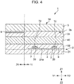
- Fig. 4 is a cross-sectional view on cross section C2-C2 indicated in Fig. 2 .
- a transparent electrode since a transparent electrode is transparent, it cannot be originally viewed. In Fig. 2 , however, the outline shapes of transparent electrodes are illustrated for easy understanding.
- transparency and translucent property indicate a state in which visible light transmittance is 50% or higher (preferably, 80% or higher). Furthermore, it is preferable for the haze value to be 6% or lower. In this application, “light shielding” and “light shielding property” indicate a state in which visible light transmittance is lower than 50% (preferably, lower than 20%).
- the capacitive sensor 1 has a sensor substrate 2, a panel 3, an intermediate layer 40, a first adhesive layer 31, and a second adhesive layer 32.
- the panel 3 has a translucent property and is formed from, for example, a material including a resin such as polycarbonate (PC).
- the sensor substrate 2 is provided at a position distant from the panel 3. Specifically, the sensor substrate 2 is provided at, for example, a position close to a display device 51 such as a liquid crystal display or an organic EL device when viewed from the panel 3, and is attached to a case 52 or the like that holds the display device 51.
- the sensor substrate 2 is referred to as, for example, a glass sensor, and has a base material 21 (see Fig. 3 ) made of glass and transparent electrodes. Details of the sensor substrate 2 will be described later.
- the intermediate layer 40 is provided between the panel 3 and the sensor substrate 2.
- the intermediate layer 40 has a translucent property and is formed from, for example, a material including a resin such as polyethylene terephthalate (PET).
- PET polyethylene terephthalate
- the linear expansion coefficient of the intermediate layer 40 is larger than the linear expansion coefficient of the base material 21 of the sensor substrate 2 and is smaller than the linear expansion coefficient of the panel 3.
- the Young's modulus of the intermediate layer 40 is lower than the Young's modulus of the base material 21 of the sensor substrate 2 and is higher than the Young's modulus of the panel 3.
- the first adhesive layer 31 is provided between the panel 3 and the intermediate layer 40 and mutually bonds the panel 3 and intermediate layer 40.
- the second adhesive layer 32 is provided between the sensor substrate 2 and the intermediate layer 40 and mutually bonds the sensor substrate 2 and intermediate layer 40.
- the Young's modulus of each of the first adhesive layer 31 and second adhesive layer 32 is lower than the Young's modulus of the panel 3, the Young's modulus of the base material 21 of the sensor substrate 2, and the Young's modulus of the intermediate layer 40.
- Each of the first adhesive layer 31 and second adhesive layer 32 is an optical clear adhesive (OCA) layer and is composed of, for example, an adhesive layer including an acrylic adhesive, a double-sided adhesive tape, or the like.
- the capacitive sensor 1 is composed of a detection area 11 and a non-detection area 25 when viewed from a direction (Z1-Z2 direction) along the normal of a surface on the same side as the panel 3.
- the detection area 11 is an area on which a manipulation can be performed with a manipulation body such as a finger F
- the non-detection area 25 is an area, shaped like a picture frame, that is positioned on the outer circumference side of the detection area 11.
- the non-detection area 25 is light-shielded by a decorative layer 9 described later.
- the capacitive sensor 1 In the capacitive sensor 1, light (exemplified by external light) from a surface on the same side as the panel 3 toward a surface on the same side as the sensor substrate 2 and light (exemplified by light from a backlight of the display device 51 used in combination with the capacitive sensor 1) from the surface on the same side as the sensor substrate 2 toward the surface on the same side as the panel 3 are less likely to pass through the non-detection area 25.
- the sensor substrate 2 in this embodiment has the base material 21, first electrodes 8, and second electrodes 12.
- the first electrode 8 is placed in the detection area 11 and has a plurality of first transparent electrodes 4. As illustrated in Fig. 4 , the plurality of first transparent electrodes 4 are provided on a main surface (sometimes simply referred to below as the "front surface") 21a, which is one of the main surfaces of the base material 21 and is positioned on the Z1 side, the normal of the main surfaces being along the Z1-Z2 direction. Each first transparent electrode 4 is linked through an elongated linking part 7 in the Y1-Y2 direction (first direction).
- the first electrodes 8, each of which has a plurality of first transparent electrodes 4 linked in the Y1-Y2 direction, are arranged in the X1-X2 direction at intervals.
- the first transparent electrode 4 and linking part 7 are formed from a transparent conductive material such as ITO (Indium Tin Oxide) by sputtering, evaporation, or the like.
- transparent conductive materials include metal nanowires typified by silver nanowires, thin metals formed in a mesh shape, conductive polymers, or the like. This is also true for transparent conductive materials described later.
- the second electrode 12 is placed in the detection area 11 and has a plurality of second transparent electrodes 5.
- the plurality of second transparent electrodes 5 are provided on the front surface 21a of the base material 21.
- the second transparent electrodes 5 are provided on the same surface (front surface 21a of the base material 21) as the first transparent electrodes 4.
- each second transparent electrode 5 is linked through an elongated bridge wire 10 in the X1-X2 direction (second direction).
- the second electrodes 12, each of which has a plurality of second transparent electrodes 5 linked in the X1-X2 direction, are arranged in the Y1-Y2 direction at intervals.
- the X1-X2 direction crosses the Y1-Y2 direction.
- the X1-X2 direction perpendicularly crosses the Y1-Y2 direction.
- the second transparent electrode 5 is formed from a transparent conductive material such as ITO by sputtering, evaporation, or the like.
- the bridge wire 10 is formed from a transparent conductive material such as ITO.
- the bridge wire 10 may have a first layer including a transparent conductive material such as ITO and a second layer composed of a metal that has a lower resistance than the first layer and is transparent. If the bridge wire 10 has a laminated structure composed of the first layer and second layer, it is preferable for the second layer to be formed from any one selected from a group of Au, an Au alloy, CuNi, and Ni. Of these, selection of Au is more preferable. If the second layer is formed from Au, the bridge wire 10 can obtain a superior resistance to an environment (moisture resistance and heat resistance).
- an insulative layer 20 is provided on the front surface of the linking part 7, which links individual first transparent electrodes 4. As illustrated in Fig. 3 , the insulative layer 20 fills space between the linking part 7 and the second transparent electrode 5 and also slightly rides on the front surface of the second transparent electrode 5. As the insulative layer 20, a novolak resin (resist), for example, is used.
- the bridge wire 10 is provided from the front surface 20a of the insulative layer 20 to the front surfaces of the individual second transparent electrodes 5 positioned at both sides of the insulative layer 20 in the X1-X2 direction.
- the bridge wire 10 electrically connects individual second transparent electrodes 5.
- the insulative layer 20 is provided on the front surface of the linking part 7, which links individual first transparent electrodes 4, and the bridge wire 10, which connects individual second transparent electrode 5, is provided on the front surface of the insulative layer 20.
- the insulative layer 20 intervenes between the linking part 7 and the bridge wire 10 and the first transparent electrode 4 and second transparent electrode 5 are in a state in which they are electrically insulated from each other. Since, in this embodiment, the first transparent electrode 4 and second transparent electrode 5 are provided on the same surface (front surface 21a of the base material 21), the thinning of the capacitive sensor 1 can be realized.
- the linking part 7, insulative layer 20, and bridge wire 10 are all positioned in the detection area 11 and have a translucent property as is the first transparent electrode 4 and second transparent electrode 5.
- each wiring part 6 is connected to an external connection part 27 that is electrically connected to a flexible printed circuit board. That is, each wiring part 6 electrically connects the first electrode 8, second electrode 12, and external connection part 27.
- the external connection part 27 is electrically connected to the flexible printed circuit board through, for example, a conductive paste.
- Each wiring part 6 is formed from a material that has a metal such as Cu, a Cu alloy, a CuNi alloy, Ni, Ag, Au, or the like.
- the connection wire 16 is formed from a transparent conductive material such as ITO and extends from the detection area 11 to the non-detection area 25.
- the wiring part 6 is laminated on the connection wire 16 in the non-detection area 25 and is electrically connected to the connection wire 16.
- the wiring part 6 is provided in a portion positioned in the non-detection area 25 on the front surface 21a of the base material 21.
- the external connection part 27 is also provided in a portion positioned in the non-detection area 25 on the front surface 21a of the base material 21, as is the wiring part 6.
- the panel 3 is provided so as to face the front surface 21a of the base material 21 in practice, as illustrated in Fig. 3 and Fig. 4 .
- a main surface (main surface opposite to a main surface 3b facing the front surface 21a of the base material 21) 3a positioned on the Z1 side becomes a surface on a side on which the capacitive sensor 1 is manipulated, so the manipulation surface 3a is also referred to as the "manipulation surface" in this description.
- the panel 3 may have a laminated structure.
- laminated structures include a laminated structure in which a hard coat layer formed from an inorganic material is formed on a film formed from an organic material.
- the shape of the panel 3 may be a flat-plate-like shape or may be another shape.
- the manipulation surface 3a of the panel 3 may be a curved surface.
- the surface shapes of the manipulation surface 3a and main surface 3b of the panel 3 may be different; of the main surfaces of the panel 3 that have a normal along the Z1-Z2 direction, the main surface 3b is the main surface positioned on the Z2 side (in other words, the main surface 3b is a main surface opposite to the manipulation surface 3a, so the main surface 3b may also be simply referred to below as the "rear surface").
- the decorative layer 9 that has a shielding property is provided in a portion positioned in the non-detection area 25 on the rear surface 3b of the panel 3.
- the decorative layer 9 is provided in the whole of the portion positioned in the non-detection area 25 on the rear surface 3b of the panel 3. Therefore, the wiring parts 6 and external connection parts 27 are hidden by the decorative layer 9 and are not viewed when the capacitive sensor 1 is viewed from the same side as the manipulation surface 3a of the panel 3.
- the material forming the decorative layer 9 is any material if it has a shielding property.
- the decorative layer 9 may have an insulation property.
- the capacitive sensor 1 illustrated in Fig. 1 when the finger F used as an example of a manipulation body is caused to come into contact with the manipulation surface 3a of the panel 3 as illustrated in Fig. 3 , a capacitance is generated between the finger F and the first transparent electrode 4 close to the finger F and between the finger F and the second transparent electrode 5 close to the finger F.
- the capacitive sensor 1 can calculate the contact position of the finger F according to a change in capacitance at that time.
- the capacitive sensor 1 detects the X coordinate of the position of the finger F according to a change in capacitance between the finger F and the first electrode 8 and detects the Y coordinate of the position of the finger F according to a change in capacitance between the finger F and the second electrode 12 (self-capacitance detection type).
- the capacitive sensor 1 may be of mutual capacitance detection type. That is, the capacitive sensor 1 may apply a driving voltage to a string of electrodes, which is any one of the first electrode 8 and second electrode 12, and may detect a change in capacitance between the finger F and the other of the first electrode 8 and the second electrode 12. Due to this, the capacitive sensor 1 detects the Y coordinate of the position of the finger F from the other electrode and detects the X direction of the position of the finger F from one electrode.
- the placement of the first transparent electrodes 4 and second transparent electrodes 5 represented in Fig. 2 to Fig. 4 is just an example and is not limited only to this.
- the capacitive sensor 1 is only required to be capable of detecting a change in capacitance between a manipulation body such as the finger F and a transparent electrode and calculating the contact position of the manipulation body to the manipulation surface 3a.
- the first transparent electrodes 4 and second transparent electrodes 5 may be provided on the different main surfaces of the base material 21.
- the capacitive sensor 1 may be used as a vehicle-mounted sensor.
- the shape of the base material 21 of the sensor substrate 2 placed at a position near the display device 51 is often rectangular when viewed from the panel 3.
- the shape of the panel 3, a main surface of which is the manipulation surface 3a is not limited only to a rectangular shape but may become various shapes.
- the shape of the panel 3 represents various shapes depending on the shape of the instrument panel of the vehicle.
- the form of fixing the panel 3 is also various.
- the base material 21 and panel 3 may expand or contract in mutually different directions.
- one adhesive layer is provided between the base material and the panel, a state occurs in which a shearing force is exerted on the adhesive layer.
- the adhesive layer cannot follow at least any of the expansion and contraction of the base material 21 and panel 3, so the adhesive layer may peel off from at least any of the base material 21 and panel 3.
- the intermediate layer 40 is provided between the panel 3 and the sensor substrate 2, specifically between the panel 3 and the base material 21.
- the first adhesive layer 31, which bonds the panel 3 and intermediate layer 40 is provided between the panel 3 and the intermediate layer 40.
- the second adhesive layer 32 which bonds the sensor substrate 2 and intermediate layer 40 is provided between the sensor substrate 2 and the intermediate layer 40, specifically between the base material 21 and the intermediate layer 40. That is, two adhesive layers (first adhesive layer 31 and second adhesive layer 32) are provided on both sides of the intermediate layer 40.
- the intermediate layer 40 can cause the first adhesive layer 31 and second adhesive layer 32 to function independently on both sides of the intermediate layer 40.
- the intermediate layer 40 can separate the adhesive layer functions as the first adhesive layer 31 and second adhesive layer 32 by using the intermediate layer 40 as a boundary. Even if a shearing force is exerted on members positioned between the panel 3 and the sensor substrate 2 because, for example, environment temperature around the capacitive sensor 1 changes and the resinous panel 3 and glass base material 21 expand or contract in different directions, since the first adhesive layer 31 and second adhesive layer 32 are placed with the intermediate layer 40 intervening between them, they can be deformed independently of each other.
- a shearing force generated due to the displacement of the panel 3 is mainly exerted on the first adhesive layer 31 positioned between the panel 3 and the intermediate layer 40.
- the first adhesive layer 31 is deformed so as to follow a change in the relative position of the panel 3 to the intermediate layer 40, and can absorb or mitigate the shearing force exerted on the first adhesive layer 31.
- a shearing force generated due to the displacement of the base material 21 of the sensor substrate 2 is mainly exerted on the second adhesive layer 32 positioned between the base material 21 of the sensor substrate 2 and the intermediate layer 40.
- the second adhesive layer 32 is deformed so as to follow a change in the relative position of the base material 21 of the sensor substrate 2 to the intermediate layer 40, and can absorb or mitigate the shearing force exerted on the second adhesive layer 32. Due to this, even if a searing force caused by a change in environment temperature or the like is exerted on the first adhesive layer 31 and second adhesive layer 32, it is possible to restrain the first adhesive layer 31 and second adhesive layer 32 from peeling off from the panel 3 and base material 21.
- the intermediate layer 40 is formed from a material including a resin, the intermediate layer 40 can be deformed relatively flexibly for a change in environment temperature.
- the linear expansion coefficient of the intermediate layer 40 is larger than the linear expansion coefficient of the base material 21 and is smaller than the linear expansion coefficient of the panel 3.
- the amount of expansion or contraction of the intermediate layer 40 is between the amount of expansion or contraction of the base material 21 and the amount of expansion or contraction of the panel 3.
- the Young's modulus of the intermediate layer 40 is lower than the Young's modulus of the base material 21 and is higher than the Young's modulus of the panel 3.
- the amount of distortion when an external force is exerted on the whole of the capacitive sensor 1 is lower at the panel 3, intermediate layer 40, and base material 21 in that order. Accordingly, when an external force is exerted on the whole of the capacitive sensor 1 and distortion in the in-main-plane-direction is thereby generated in the members constituting the capacitive sensor 1, a change in relative position caused between the panel 3 and the intermediate layer 40 and a change in relative position caused between the base material 21 and the intermediate layer 40 are smaller than a change in relative position caused between the panel 3 and the base material 21.
- the Young's modulus of each of the first adhesive layer 31 and second adhesive layer 32 is lower than the Young's modulus of the panel 3, the Young's modulus of the base material 21, and the Young's modulus of the intermediate layer 40. Therefore, the first adhesive layer 31 and second adhesive layer 32 can flexibly follow a change in relative position between the panel 3 and the intermediate layer 40 and a change in relative position between the base material 21 and the intermediate layer 40, which are caused by the deformation of the panel 3, base material 21, and intermediate layer 40.
- first adhesive layer 31 and second adhesive layer 32 include an acrylic adhesive resin, it is possible to flexibly follow a change in relative position between the panel 3 and the intermediate layer 40 and a change in relative position between the base material 21 and the intermediate layer 40, which are caused by the deformation of the panel 3, base material 21, and intermediate layer 40 while optical performance (appropriateness of permeability and refractive index and the like) is secured.
- Fig. 5 is an exploded view representing a model in the simulation executed by the present inventor.
- Fig. 6 is a table that compiles individual members of the model in this simulation.
- Fig. 7 is drawings that explain constraint conditions in this simulation.
- Fig. 8 is a table that compiles an example of results in this simulation.
- Fig. 9 is an exploded view representing a model according to a comparative example.
- Fig. 7(a) is a plan view representing an area used in the simulation.
- Fig. 7(b) is a perspective view representing a one-fourth model used in the simulation.
- the present inventor performed a simulation related to the capacitive sensor 1 according to this embodiment. That is, the present inventor confirmed, from the simulation, stress exerted on the first adhesive layer 31 and second adhesive layer 32 when environment temperature around the capacitive sensor 1 was raised from 20°C to 95°C.
- a model 1A, used in this simulation, of the capacitive sensor 1 has the sensor substrate 2, panel 3, intermediate layer 40, first adhesive layer 31, and second adhesive layer 32.
- the material, thickness (millimeters: mm), Young's modulus (pascals: Pa), Poisson's ratio, and linear expansion coefficient (/°C) of the individual members of the model 1A are as in the table represented in Fig. 6 .
- the material of the panel 3 is polycarbonate (PC).
- the material of the first adhesive layer 31 and second adhesive layer 32 is an acrylic adhesive.
- the material of the intermediate layer 40 is polyethylene terephthalate (PET).
- PET polyethylene terephthalate
- the material of the base material 21 of the sensor substrate 2 is SiO 2 .
- the thickness of the panel 3 is 1 mm.
- the thickness of each of the first adhesive layer 31 and second adhesive layer 32 is 0.1 mm.
- the thickness of the intermediate layer 40 is 0.05 mm.
- the thickness of the base material 21 is 0.7 mm.
- the linear expansion coefficient (2 ⁇ 10 -5 ) of the intermediate layer 40 is larger than the linear expansion coefficient (8 ⁇ 10 -6 ) of the base material 21 and is smaller than the linear expansion coefficient (7 ⁇ 10 -5 ) of the panel 3.
- the Young's modulus (6.2 ⁇ 10 9 ) of the intermediate layer 40 is lower than the Young's modulus (8.01 ⁇ 10 10 ) of the base material 21 and is higher than the Young's modulus (2.45 ⁇ 10 9 ) of the panel 3.
- the Young's modulus (9.9 ⁇ 10 5 ) of each of the first adhesive layer 31 and second adhesive layer 32 is lower than the Young's modulus (2.45 ⁇ 10 9 ) of the panel 3, the Young's modulus (8.01 ⁇ 10 10 ) of the base material 21, and the Young's modulus (6.2 ⁇ 10 9 ) of the intermediate layer 40.
- the direction along the normal of the main surfaces of the panel 3 or base material 21 will be the Z direction. Also, one of the directions along the main surfaces of the panel 3 or base material 21 is the X direction, and the direction perpendicular to the Z direction and X direction is the Y direction.
- a simulation was performed by using a one-fourth model 1A of the capacitive sensor 1.
- the base material 21 of the sensor substrate 2 was constrained in the Z direction.
- cross sections 13A of the area A11 along the Y direction were symmetrically constrained in the X direction.
- cross sections 13B of the area A11 along X direction were symmetrically constrained in the Y direction.
- the maximum stress exerted on the first adhesive layer 31 was 0.785 MPa.
- the maximum stress exerted on the second adhesive layer 32 was 0.670 MPa.
- the maximum stress exerted on an adhesive layer 31A was 0.892 MPa.
- the model 1B of the capacitive sensor according to the comparative example has the sensor substrate 2, panel 3, and adhesive layer 31A. That is, the model 1B of the capacitive sensor according to the comparative example does not have an intermediate layer. Therefore, one adhesive layer 31A is provided between the sensor substrate 2 and the panel 3. That is, the functions of the adhesive layer 31A are not separated.
- each of the base material of the sensor substrate 2, the panel 3, and the adhesive layer 31A in the model 1B in the comparative example are the same as the conditions of each of the base material 21 of the sensor substrate 2, panel 3, and first adhesive layer 31, which have been described in relation to Fig. 6 .
- the maximum stress (0.785 MPa) exerted on the first adhesive layer 31 is reduced by 12% when compared with the maximum stress (0.892 MPa) exerted on the adhesive layer 31A of the model 1B in the comparative example.
- the maximum stress (0.670 MPa) exerted on the second adhesive layer 32 is reduced by 24.9% when compared with the maximum stress (0.892 MPa) exerted on the adhesive layer 31A of the model 1B in the comparative example.
- Fig. 10 is a table that compiles individual members of a model in the other simulation performed by the present inventor.
- Fig. 11 is a table that compiles an example of results in this simulation.
- the thickness of each of the first adhesive layer 31 and second adhesive layer 32 is 0.4 mm.
- the thickness of each of other members is the same as the thickness of each member in the simulation described above in relation to Fig. 5 to Fig. 9 .
- the Young's modulus, Poisson's ratio, and linear expansion coefficient of each member are the same as the Young's modulus, Poisson's ratio, and linear expansion coefficient of each member in the simulation described above in relation to Fig. 5 to Fig. 9 .
- constraint conditions are the same as the constraint conditions in the simulation described above in relation to Fig. 5 to Fig. 9 . That is, this simulation differs from the simulation described above in relation to Fig. 5 to Fig. 9 in the thickness of each of the first adhesive layer 31 and second adhesive layer 32.
- the maximum stress (0.320 MPa) exerted on the first adhesive layer 31 is reduced by 64.1% when compared with the maximum stress (0.892 MPa) exerted on the adhesive layer 31A of the model 1B in the comparative example.
- the maximum stress (0.257 MPa) exerted on the second adhesive layer 32 is reduced by 71.2% when compared with the maximum stress (0.892 MPa) exerted on the adhesive layer 31A of the model 1B in the comparative example.
- the present invention is not limited to these examples.
- the scope of the present invention also includes embodiments obtained as a result of adding or deleting constituent element to or from the above each embodiment or its application examples, performing design changes to the above embodiment or its application examples, or appropriately combining features in each embodiment; the addition, deletion, design change, or combination is effected by a person having ordinary skill in the art without departing from the intended scope of the present invention.
- the decorative layer 9 is provided over the whole of the portion, on the rear surface 3b of the panel 3, in which the non-detection area 25 is located, and the whole of the non-detection area 25 is light-shielded, but the present invention is not limited to this.
- the portion, on the rear surface 3b of the panel 3, in which the non-detection area 25 is located may include a portion in which the decorative layer 9 is not provided.
- the decorative layer 9 is provided on the rear surface 3b of the panel 3, the present invention is not limited to this; the decorative layer 9 is only required to be positioned between the panel 3 and the base material 21.
- the decorative layer 9 may be buried in the first adhesive layer 31.
Landscapes
- Engineering & Computer Science (AREA)
- General Engineering & Computer Science (AREA)
- Theoretical Computer Science (AREA)
- Human Computer Interaction (AREA)
- Physics & Mathematics (AREA)
- General Physics & Mathematics (AREA)
- Position Input By Displaying (AREA)
- Laminated Bodies (AREA)
Abstract
Description
- The present invention relates to a capacitive sensor, and more particularly to a capacitive sensor that has a resinous panel and a glass base material.
- In
PTL 1, a laminated body, for use for a touch panel, in which an adhesive sheet is placed between a protective substrate and a capacitive touch panel sensor is disclosed. The capacitive touch panel sensor described inTPL 1 has a substrate, a first detection electrode, and a second detection electrode. Examples of the substrate include a glass substrate and the like. It is preferable for the protective substrate to be a transparent substrate. Examples of the protective substrate include a plastic plate and the like. - Also, in
PTL 1, a capacitive touch panel in which an adhesive sheet is placed between a display device and a capacitive touch panel sensor is disclosed. Examples of the display device described inPTL 1 include, for example, a cathode-ray tube (CRT) display, a liquid crystal display (LCD), an organic light emitting diode (OLED) display, a vacuum fluorescent display (VFD), a plasma display panel (PDP), a surface electric field display (SED), a field emission display (FED), electric paper (E-paper), and the like. - PTL 1: Japanese Unexamined Patent Application Publication No.
2015-172921 - A capacitive touch panel may be used as a vehicle-mounted sensor as is, for example, a sensor mounted in car navigation or the like. At that time, while the shape of a glass substrate placed at a position near a display device is often rectangular, the shape of a protective substrate placed at a position near a manipulation surface or the shape of a protective substrate a main surface of which is a manipulation surface is not limited only to a rectangular shape but may become various shapes. The form of fixing the protective substrate is various.
- In this case, when environment temperature around the capacitive touch panel changes, the glass substrate and protective substrate may expand or contract in mutually different directions. Then, a state occurs in which a shearing force is exerted on the adhesive sheet placed between the protective substrate and the capacitive touch panel sensor. At that time, if the adhesive force of the adhesive sheet to the protective substrate and capacitive touch panel sensor is low, the adhesive sheet may peel off from at least any of the protective substrate and capacitive touch panel sensor.
- The present invention addresses the conventional problem described above with the object of providing a capacitive sensor that can restrain an adhesive layer from peeling off even if a shearing force caused by a change in environment temperature or the like is exerted on the adhesive layer.
- In one aspect, a capacitive sensor in the present invention is characterized by having: a resinous panel that has a translucent property, one main surface of the panel being a manipulation surface; a sensor substrate placed so as to face a main surface of the panel, the main surface being opposite to the manipulation surface of the panel, the sensor substrate having a glass base material and a transparent electrode provided on at least one main surface of the base material; an intermediate layer that has a translucent property, the intermediate layer being provided between the panel and the sensor substrate; a first adhesive layer provided between the panel and the intermediate layer, the first adhesive layer bonding the panel and the intermediate layer; and a second adhesive layer provided between the sensor substrate and the intermediate layer, the second adhesive layer bonding the sensor substrate and the intermediate layer.
- In the capacitive sensor described above, an intermediate layer that has a translucent property is provided between a resinous panel one main surface of which is a manipulation surface and a sensor substrate that has a glass base material and a transparent electrode. A first adhesive layer that bonds the panel and intermediate layer is provided between the panel and the intermediate layer. Also, a second adhesive layer that bonds the sensor substrate and intermediate layer is provided between the sensor substrate and the intermediate layer. That is, two adhesive layers are provided on both sides of the intermediate layer.
- Due to this, the intermediate layer can cause two adhesive layers to function independently on both sides of the intermediate layer. In other words, the intermediate layer can separate the adhesive layer functions by using the intermediate layer as a boundary. Even if a shearing force is exerted on members positioned between the panel and the sensor substrate because, for example, environment temperature around the capacitive sensor changes and the resinous panel and glass base material expand or contract in different directions, since the first adhesive layer and second adhesive layer are placed with the intermediate layer intervening between them, they can be deformed independently of each other. That is, a shearing force generated due to the displacement of the panel is mainly exerted on the first adhesive layer positioned between the panel and the intermediate layer. At that time, the first adhesive layer is deformed so as to follow a change in the relative position of the panel to the intermediate layer, and can absorb or mitigate the shearing force exerted on the first adhesive layer. Also, a shearing force generated due to the displacement of the base material is mainly exerted on the second adhesive layer positioned between the base material and the intermediate layer. At that time, the second adhesive layer is deformed so as to follow a change in the relative position of the base material of the sensor substrate to the intermediate layer, and can absorb or mitigate the shearing force exerted on the second adhesive layer. Due to this, it is possible to restrain the first adhesive layer and second adhesive layer from peeling off from the panel and base material.
- In the capacitive sensor described above, the intermediate layer may be formed from a material including a resin, and the linear expansion coefficient of the intermediate layer may be larger than the linear expansion coefficient of the base material and may be smaller than the linear expansion coefficient of the panel.
- In this case, the intermediate layer is formed from a material including a resin, so the intermediate layer is deformed relatively flexibly for a change in environment temperature. Also, the linear expansion coefficient of the intermediate layer is larger than the linear expansion coefficient of the base material and is smaller than the linear expansion coefficient of the panel. Thus, the amount of expansion or contraction of the intermediate layer is between the amount of expansion or contraction of the base material and the amount of expansion or contraction of the panel. Accordingly, when the panel, intermediate layer, and base material expand or contract according to a change in environment temperature, a change of the relative position of the panel to the intermediate layer and a change of the relative position of the base material to the intermediate layer are smaller than a change in the relative position between the panel and the base material. Therefore, when compared with a case in which only an adhesive layer (contrast adhesive layer) is provided between the panel and the base material without the intermediate layer being provided, when environment temperature changes, a shearing force exerted on each of the first adhesive layer and second adhesive layer is lower than a shearing force exerted on the above contrast adhesive layer. Due to this, it is possible to more stably restrain the possibility that the first adhesive layer and second adhesive layer peel off from the panel and base material.
- The Young's modulus of the intermediate layer may be lower than the Young's modulus of the base material and may be higher than the Young's modulus of the panel. In this case, the amount of distortion when an external force is exerted on the whole of the capacitive sensor is lower at the panel, intermediate layer, and base material in that order. Accordingly, when an external force is exerted on the whole of the capacitive sensor and distortion in the in-main-plane-direction is thereby generated in the members constituting the capacitive sensor, a change in relative position caused between the panel and the intermediate layer and a change in relative position caused between the base material and the intermediate layer are smaller than a change in relative position caused between the panel and the base material. Therefore, when compared with a case in which only an adhesive layer (contrast adhesive layer) is provided between the panel and the base material without the intermediate layer being provided, when an external force is exerted on the whole of the capacitive sensor and distortion is thereby generated in the members constituting the capacitive sensor, a shearing forces exerted on each of the first adhesive layer and second adhesive layer is lower than a shearing force exerted on the above contrast adhesive layer. Due to this, it is possible to more stably restrain the possibility that the first adhesive layer and second adhesive layer peel off from the panel and base material.
- The Young's modulus of each of the first adhesive layer and second adhesive layer may be lower than the Young's modulus of the panel, the Young's modulus of the base material, and the Young's modulus of the intermediate layer. In this case, since the Young's modulus of each of the first adhesive layer and the second adhesive layer is lower than the Young's modulus of the panel, the Young's modulus of the base material, and the Young's modulus of the intermediate layer, the first adhesive layer and second adhesive layer can flexibly follow a change in relative position between the panel and the intermediate layer and a change in relative position between the base material and the intermediate layer, which are caused by the deformation of the panel, base material, and intermediate layer. Therefore, even if shearing forces caused by the deformation of the panel, base material, and intermediate layer are exerted on the first adhesive and second adhesive layer, these shearing forces can be appropriately absorbed or mediated in the interiors of the first adhesive layer and second adhesive layer.
- The first adhesive layer and the second adhesive layer may include an acrylic adhesive resin. In this case, the first adhesive layer and second adhesive layer can flexibly follow a change in relative position between the panel and the intermediate layer and a change in relative position between the base material and the intermediate layer, which are caused by the deformation of the panel, base material, and intermediate layer, while optical performance is secured.
- According to the present invention, a capacitive sensor is provided that can restrain an adhesive layer from peeling off even if environment temperature changes.
-
-
Fig. 1 is an exploded view representing a capacitive sensor according to this embodiment. -
Fig. 2 is a plan view representing the structure of the capacitive sensor according to this embodiment. -
Fig. 3 is a cross-sectional view on cross section C1-C1 represented inFig. 2 . -
Fig. 4 is a cross-sectional view on cross section C2-C2 represented inFig. 2 . -
Fig. 5 is an exploded view representing a model in a simulation performed by the present inventor. -
Fig. 6 is a table that compiles individual members of the model in this simulation. -
Fig. 7 is drawings that explain constraint conditions in this simulation. -
Fig. 8 is a table that compiles an example of results in this simulation. -
Fig. 9 is an exploded view representing a model according to a comparative example. -
Fig. 10 is a table that compiles individual members of a model in another simulation performed by the present inventor. -
Fig. 11 is a table that compiles an example of results in this simulation. - An embodiment of the present invention will be described with reference to the drawings. In the individual drawings, like elements are assigned like reference characters and detailed descriptions will be appropriately omitted.
-
Fig. 1 is an exploded view representing a capacitive sensor according to this embodiment. -
Fig. 2 is a plan view representing the structure of the capacitive sensor according to this embodiment. -
Fig. 3 is a cross-sectional view on cross section C1-C1 indicated inFig. 2 . -
Fig. 4 is a cross-sectional view on cross section C2-C2 indicated inFig. 2 . - Incidentally, since a transparent electrode is transparent, it cannot be originally viewed. In
Fig. 2 , however, the outline shapes of transparent electrodes are illustrated for easy understanding. - In this application, "transparency" and "translucent property" indicate a state in which visible light transmittance is 50% or higher (preferably, 80% or higher). Furthermore, it is preferable for the haze value to be 6% or lower. In this application, "light shielding" and "light shielding property" indicate a state in which visible light transmittance is lower than 50% (preferably, lower than 20%).
- As represented in
Fig. 1 , thecapacitive sensor 1 according to this embodiment has asensor substrate 2, apanel 3, anintermediate layer 40, a firstadhesive layer 31, and a secondadhesive layer 32. Thepanel 3 has a translucent property and is formed from, for example, a material including a resin such as polycarbonate (PC). - The
sensor substrate 2 is provided at a position distant from thepanel 3. Specifically, thesensor substrate 2 is provided at, for example, a position close to adisplay device 51 such as a liquid crystal display or an organic EL device when viewed from thepanel 3, and is attached to acase 52 or the like that holds thedisplay device 51. Thesensor substrate 2 is referred to as, for example, a glass sensor, and has a base material 21 (seeFig. 3 ) made of glass and transparent electrodes. Details of thesensor substrate 2 will be described later. - The
intermediate layer 40 is provided between thepanel 3 and thesensor substrate 2. Theintermediate layer 40 has a translucent property and is formed from, for example, a material including a resin such as polyethylene terephthalate (PET). The linear expansion coefficient of theintermediate layer 40 is larger than the linear expansion coefficient of thebase material 21 of thesensor substrate 2 and is smaller than the linear expansion coefficient of thepanel 3. The Young's modulus of theintermediate layer 40 is lower than the Young's modulus of thebase material 21 of thesensor substrate 2 and is higher than the Young's modulus of thepanel 3. - The first
adhesive layer 31 is provided between thepanel 3 and theintermediate layer 40 and mutually bonds thepanel 3 andintermediate layer 40. The secondadhesive layer 32 is provided between thesensor substrate 2 and theintermediate layer 40 and mutually bonds thesensor substrate 2 andintermediate layer 40. The Young's modulus of each of the firstadhesive layer 31 and secondadhesive layer 32 is lower than the Young's modulus of thepanel 3, the Young's modulus of thebase material 21 of thesensor substrate 2, and the Young's modulus of theintermediate layer 40. Each of the firstadhesive layer 31 and secondadhesive layer 32 is an optical clear adhesive (OCA) layer and is composed of, for example, an adhesive layer including an acrylic adhesive, a double-sided adhesive tape, or the like. - As represented in
Fig. 2 to Fig. 4 , thecapacitive sensor 1 is composed of adetection area 11 and anon-detection area 25 when viewed from a direction (Z1-Z2 direction) along the normal of a surface on the same side as thepanel 3. Thedetection area 11 is an area on which a manipulation can be performed with a manipulation body such as a finger F, and thenon-detection area 25 is an area, shaped like a picture frame, that is positioned on the outer circumference side of thedetection area 11. Thenon-detection area 25 is light-shielded by adecorative layer 9 described later. In thecapacitive sensor 1, light (exemplified by external light) from a surface on the same side as thepanel 3 toward a surface on the same side as thesensor substrate 2 and light (exemplified by light from a backlight of thedisplay device 51 used in combination with the capacitive sensor 1) from the surface on the same side as thesensor substrate 2 toward the surface on the same side as thepanel 3 are less likely to pass through thenon-detection area 25. - The
sensor substrate 2 in this embodiment has thebase material 21,first electrodes 8, andsecond electrodes 12. - The
first electrode 8 is placed in thedetection area 11 and has a plurality of firsttransparent electrodes 4. As illustrated inFig. 4 , the plurality of firsttransparent electrodes 4 are provided on a main surface (sometimes simply referred to below as the "front surface") 21a, which is one of the main surfaces of thebase material 21 and is positioned on the Z1 side, the normal of the main surfaces being along the Z1-Z2 direction. Each firsttransparent electrode 4 is linked through anelongated linking part 7 in the Y1-Y2 direction (first direction). Thefirst electrodes 8, each of which has a plurality of firsttransparent electrodes 4 linked in the Y1-Y2 direction, are arranged in the X1-X2 direction at intervals. - The first
transparent electrode 4 and linkingpart 7 are formed from a transparent conductive material such as ITO (Indium Tin Oxide) by sputtering, evaporation, or the like. Besides ITO, transparent conductive materials include metal nanowires typified by silver nanowires, thin metals formed in a mesh shape, conductive polymers, or the like. This is also true for transparent conductive materials described later. - The
second electrode 12 is placed in thedetection area 11 and has a plurality of secondtransparent electrodes 5. As illustrated inFig. 3 , the plurality of secondtransparent electrodes 5 are provided on thefront surface 21a of thebase material 21. Thus, the secondtransparent electrodes 5 are provided on the same surface (front surface 21a of the base material 21) as the firsttransparent electrodes 4. As illustrated inFig. 3 andFig. 4 , each secondtransparent electrode 5 is linked through anelongated bridge wire 10 in the X1-X2 direction (second direction). Thesecond electrodes 12, each of which has a plurality of secondtransparent electrodes 5 linked in the X1-X2 direction, are arranged in the Y1-Y2 direction at intervals. Incidentally, the X1-X2 direction crosses the Y1-Y2 direction. For example, the X1-X2 direction perpendicularly crosses the Y1-Y2 direction. - The second
transparent electrode 5 is formed from a transparent conductive material such as ITO by sputtering, evaporation, or the like. Thebridge wire 10 is formed from a transparent conductive material such as ITO. Alternatively, thebridge wire 10 may have a first layer including a transparent conductive material such as ITO and a second layer composed of a metal that has a lower resistance than the first layer and is transparent. If thebridge wire 10 has a laminated structure composed of the first layer and second layer, it is preferable for the second layer to be formed from any one selected from a group of Au, an Au alloy, CuNi, and Ni. Of these, selection of Au is more preferable. If the second layer is formed from Au, thebridge wire 10 can obtain a superior resistance to an environment (moisture resistance and heat resistance). - As illustrated in
Fig. 3 andFig. 4 , aninsulative layer 20 is provided on the front surface of the linkingpart 7, which links individual firsttransparent electrodes 4. As illustrated inFig. 3 , theinsulative layer 20 fills space between the linkingpart 7 and the secondtransparent electrode 5 and also slightly rides on the front surface of the secondtransparent electrode 5. As theinsulative layer 20, a novolak resin (resist), for example, is used. - As illustrated in
Fig. 3 andFig. 4 , thebridge wire 10 is provided from thefront surface 20a of theinsulative layer 20 to the front surfaces of the individual secondtransparent electrodes 5 positioned at both sides of theinsulative layer 20 in the X1-X2 direction. Thebridge wire 10 electrically connects individual secondtransparent electrodes 5. - As illustrated in
Fig. 3 andFig. 4 , theinsulative layer 20 is provided on the front surface of the linkingpart 7, which links individual firsttransparent electrodes 4, and thebridge wire 10, which connects individual secondtransparent electrode 5, is provided on the front surface of theinsulative layer 20. Thus, theinsulative layer 20 intervenes between the linkingpart 7 and thebridge wire 10 and the firsttransparent electrode 4 and secondtransparent electrode 5 are in a state in which they are electrically insulated from each other. Since, in this embodiment, the firsttransparent electrode 4 and secondtransparent electrode 5 are provided on the same surface (front surface 21a of the base material 21), the thinning of thecapacitive sensor 1 can be realized. - Incidentally, the linking
part 7,insulative layer 20, andbridge wire 10 are all positioned in thedetection area 11 and have a translucent property as is the firsttransparent electrode 4 and secondtransparent electrode 5. - As illustrated in
Fig. 2 , a plurality ofwiring parts 6 led out from individualfirst electrodes 8 and individualsecond electrodes 12 are formed in thenon-detection area 25. Each of thefirst electrode 8 andsecond electrode 12 is electrically connected to thewiring part 6 through aconnection wire 16. As illustrated inFig. 2 , eachwiring part 6 is connected to anexternal connection part 27 that is electrically connected to a flexible printed circuit board. That is, eachwiring part 6 electrically connects thefirst electrode 8,second electrode 12, andexternal connection part 27. Theexternal connection part 27 is electrically connected to the flexible printed circuit board through, for example, a conductive paste. - Each
wiring part 6 is formed from a material that has a metal such as Cu, a Cu alloy, a CuNi alloy, Ni, Ag, Au, or the like. Theconnection wire 16 is formed from a transparent conductive material such as ITO and extends from thedetection area 11 to thenon-detection area 25. Thewiring part 6 is laminated on theconnection wire 16 in thenon-detection area 25 and is electrically connected to theconnection wire 16. - As illustrated in
Fig. 3 andFig. 4 , thewiring part 6 is provided in a portion positioned in thenon-detection area 25 on thefront surface 21a of thebase material 21. Theexternal connection part 27 is also provided in a portion positioned in thenon-detection area 25 on thefront surface 21a of thebase material 21, as is thewiring part 6. - Although, in
Fig. 2 , thewiring part 6 andexternal connection part 27 are illustrated so as to be viewed for easy understanding, thepanel 3 is provided so as to face thefront surface 21a of thebase material 21 in practice, as illustrated inFig. 3 andFig. 4 . Of the main surfaces of thepanel 3, their normal being along the Z1-Z2 direction, a main surface (main surface opposite to amain surface 3b facing thefront surface 21a of the base material 21) 3a positioned on the Z1 side becomes a surface on a side on which thecapacitive sensor 1 is manipulated, so themanipulation surface 3a is also referred to as the "manipulation surface" in this description. - The
panel 3 may have a laminated structure. Specific examples of laminated structures include a laminated structure in which a hard coat layer formed from an inorganic material is formed on a film formed from an organic material. The shape of thepanel 3 may be a flat-plate-like shape or may be another shape. For example, themanipulation surface 3a of thepanel 3 may be a curved surface. The surface shapes of themanipulation surface 3a andmain surface 3b of thepanel 3 may be different; of the main surfaces of thepanel 3 that have a normal along the Z1-Z2 direction, themain surface 3b is the main surface positioned on the Z2 side (in other words, themain surface 3b is a main surface opposite to themanipulation surface 3a, so themain surface 3b may also be simply referred to below as the "rear surface"). - The
decorative layer 9 that has a shielding property is provided in a portion positioned in thenon-detection area 25 on therear surface 3b of thepanel 3. In thecapacitive sensor 1 according to this embodiment, thedecorative layer 9 is provided in the whole of the portion positioned in thenon-detection area 25 on therear surface 3b of thepanel 3. Therefore, thewiring parts 6 andexternal connection parts 27 are hidden by thedecorative layer 9 and are not viewed when thecapacitive sensor 1 is viewed from the same side as themanipulation surface 3a of thepanel 3. The material forming thedecorative layer 9 is any material if it has a shielding property. Thedecorative layer 9 may have an insulation property. - With the
capacitive sensor 1 illustrated inFig. 1 , when the finger F used as an example of a manipulation body is caused to come into contact with themanipulation surface 3a of thepanel 3 as illustrated inFig. 3 , a capacitance is generated between the finger F and the firsttransparent electrode 4 close to the finger F and between the finger F and the secondtransparent electrode 5 close to the finger F. Thecapacitive sensor 1 can calculate the contact position of the finger F according to a change in capacitance at that time. Thecapacitive sensor 1 detects the X coordinate of the position of the finger F according to a change in capacitance between the finger F and thefirst electrode 8 and detects the Y coordinate of the position of the finger F according to a change in capacitance between the finger F and the second electrode 12 (self-capacitance detection type). - Alternatively, the
capacitive sensor 1 may be of mutual capacitance detection type. That is, thecapacitive sensor 1 may apply a driving voltage to a string of electrodes, which is any one of thefirst electrode 8 andsecond electrode 12, and may detect a change in capacitance between the finger F and the other of thefirst electrode 8 and thesecond electrode 12. Due to this, thecapacitive sensor 1 detects the Y coordinate of the position of the finger F from the other electrode and detects the X direction of the position of the finger F from one electrode. - Incidentally, the placement of the first
transparent electrodes 4 and secondtransparent electrodes 5 represented inFig. 2 to Fig. 4 is just an example and is not limited only to this. Thecapacitive sensor 1 is only required to be capable of detecting a change in capacitance between a manipulation body such as the finger F and a transparent electrode and calculating the contact position of the manipulation body to themanipulation surface 3a. For example, the firsttransparent electrodes 4 and secondtransparent electrodes 5 may be provided on the different main surfaces of thebase material 21. - As with, for example, a sensor mounted in car navigation or another sensor, the
capacitive sensor 1 may be used as a vehicle-mounted sensor. At that time, the shape of thebase material 21 of thesensor substrate 2 placed at a position near thedisplay device 51 is often rectangular when viewed from thepanel 3. By contrast, the shape of thepanel 3, a main surface of which is themanipulation surface 3a, is not limited only to a rectangular shape but may become various shapes. For example, the shape of thepanel 3 represents various shapes depending on the shape of the instrument panel of the vehicle. The form of fixing thepanel 3 is also various. - Thus, when environment temperature around the
capacitive sensor 1 changes, thebase material 21 andpanel 3 may expand or contract in mutually different directions. Here, if one adhesive layer is provided between the base material and the panel, a state occurs in which a shearing force is exerted on the adhesive layer. At that time, if the adhesive force of the adhesive layer to the base material and panel is low, the adhesive layer cannot follow at least any of the expansion and contraction of thebase material 21 andpanel 3, so the adhesive layer may peel off from at least any of thebase material 21 andpanel 3. - In contrast to this, in the
capacitive sensor 1 according to this embodiment, theintermediate layer 40 is provided between thepanel 3 and thesensor substrate 2, specifically between thepanel 3 and thebase material 21. In addition, the firstadhesive layer 31, which bonds thepanel 3 andintermediate layer 40, is provided between thepanel 3 and theintermediate layer 40. Also, the secondadhesive layer 32, which bonds thesensor substrate 2 andintermediate layer 40 is provided between thesensor substrate 2 and theintermediate layer 40, specifically between thebase material 21 and theintermediate layer 40. That is, two adhesive layers (firstadhesive layer 31 and second adhesive layer 32) are provided on both sides of theintermediate layer 40. - Due to this, the
intermediate layer 40 can cause the firstadhesive layer 31 and secondadhesive layer 32 to function independently on both sides of theintermediate layer 40. In other words, theintermediate layer 40 can separate the adhesive layer functions as the firstadhesive layer 31 and secondadhesive layer 32 by using theintermediate layer 40 as a boundary. Even if a shearing force is exerted on members positioned between thepanel 3 and thesensor substrate 2 because, for example, environment temperature around thecapacitive sensor 1 changes and theresinous panel 3 andglass base material 21 expand or contract in different directions, since the firstadhesive layer 31 and secondadhesive layer 32 are placed with theintermediate layer 40 intervening between them, they can be deformed independently of each other. That is, a shearing force generated due to the displacement of thepanel 3 is mainly exerted on the firstadhesive layer 31 positioned between thepanel 3 and theintermediate layer 40. At that time, the firstadhesive layer 31 is deformed so as to follow a change in the relative position of thepanel 3 to theintermediate layer 40, and can absorb or mitigate the shearing force exerted on the firstadhesive layer 31. Also, a shearing force generated due to the displacement of thebase material 21 of thesensor substrate 2 is mainly exerted on the secondadhesive layer 32 positioned between thebase material 21 of thesensor substrate 2 and theintermediate layer 40. At that time, the secondadhesive layer 32 is deformed so as to follow a change in the relative position of thebase material 21 of thesensor substrate 2 to theintermediate layer 40, and can absorb or mitigate the shearing force exerted on the secondadhesive layer 32. Due to this, even if a searing force caused by a change in environment temperature or the like is exerted on the firstadhesive layer 31 and secondadhesive layer 32, it is possible to restrain the firstadhesive layer 31 and secondadhesive layer 32 from peeling off from thepanel 3 andbase material 21. - Also, since the
intermediate layer 40 is formed from a material including a resin, theintermediate layer 40 can be deformed relatively flexibly for a change in environment temperature. As described above, the linear expansion coefficient of theintermediate layer 40 is larger than the linear expansion coefficient of thebase material 21 and is smaller than the linear expansion coefficient of thepanel 3. Thus, the amount of expansion or contraction of theintermediate layer 40 is between the amount of expansion or contraction of thebase material 21 and the amount of expansion or contraction of thepanel 3. Accordingly, when thepanel 3,intermediate layer 40, andbase material 21 expand or contract according to a change in environment temperature, a change of the relative position of thepanel 3 to theintermediate layer 40 and a change of the relative position of thebase material 21 to theintermediate layer 40 are smaller than a change in the relative position between thepanel 3 and thebase material 21. Therefore, when compared with a case in which only an adhesive layer (contrast adhesive layer) is provided between thepanel 3 and thebase material 21 without theintermediate layer 40 being provided, when environment temperature changes, a shearing force exerted on each of the firstadhesive layer 31 and secondadhesive layer 32 is lower than a shearing force exerted on the above contrast adhesive layer. Due to this, it is possible to more stably restrain the possibility that the firstadhesive layer 31 and second adhesive layer peel off from thepanel 3 andbase material 21. - Also, as described above, the Young's modulus of the
intermediate layer 40 is lower than the Young's modulus of thebase material 21 and is higher than the Young's modulus of thepanel 3. Thus, the amount of distortion when an external force is exerted on the whole of thecapacitive sensor 1 is lower at thepanel 3,intermediate layer 40, andbase material 21 in that order. Accordingly, when an external force is exerted on the whole of thecapacitive sensor 1 and distortion in the in-main-plane-direction is thereby generated in the members constituting thecapacitive sensor 1, a change in relative position caused between thepanel 3 and theintermediate layer 40 and a change in relative position caused between thebase material 21 and theintermediate layer 40 are smaller than a change in relative position caused between thepanel 3 and thebase material 21. Therefore, when compared with a case in which only an adhesive layer (contrast adhesive layer) is provided between thepanel 3 and thebase material 21 without theintermediate layer 40 being provided, when an external force is exerted on the whole of thecapacitive sensor 1 and distortion is thereby generated in the members constituting thecapacitive sensor 1, a shearing force exerted on each of the firstadhesive layer 31 and secondadhesive layer 32 is lower than a shearing force exerted on the above contrast adhesive layer. Due to this, it is possible to more stably restrain the possibility that the firstadhesive layer 31 and secondadhesive layer 32 peel off from thepanel 3 andbase material 21. - Also, as described above, the Young's modulus of each of the first
adhesive layer 31 and secondadhesive layer 32 is lower than the Young's modulus of thepanel 3, the Young's modulus of thebase material 21, and the Young's modulus of theintermediate layer 40. Therefore, the firstadhesive layer 31 and secondadhesive layer 32 can flexibly follow a change in relative position between thepanel 3 and theintermediate layer 40 and a change in relative position between thebase material 21 and theintermediate layer 40, which are caused by the deformation of thepanel 3,base material 21, andintermediate layer 40. Therefore, even if shearing forces caused by the deformation of thepanel 3,base material 21, andintermediate layer 40 are exerted on the firstadhesive layer 31 and secondadhesive layer 32, these shearing forces can be appropriately absorbed or mediated in the interiors of the firstadhesive layer 31 and secondadhesive layer 32. - Furthermore, if the first
adhesive layer 31 and secondadhesive layer 32 include an acrylic adhesive resin, it is possible to flexibly follow a change in relative position between thepanel 3 and theintermediate layer 40 and a change in relative position between thebase material 21 and theintermediate layer 40, which are caused by the deformation of thepanel 3,base material 21, andintermediate layer 40 while optical performance (appropriateness of permeability and refractive index and the like) is secured. - Next, a simulation performed by the present inventor will be described with reference to the drawings.
-
Fig. 5 is an exploded view representing a model in the simulation executed by the present inventor. -
Fig. 6 is a table that compiles individual members of the model in this simulation. -
Fig. 7 is drawings that explain constraint conditions in this simulation. -
Fig. 8 is a table that compiles an example of results in this simulation. -
Fig. 9 is an exploded view representing a model according to a comparative example. -
Fig. 7(a) is a plan view representing an area used in the simulation.Fig. 7(b) is a perspective view representing a one-fourth model used in the simulation. - The present inventor performed a simulation related to the
capacitive sensor 1 according to this embodiment. That is, the present inventor confirmed, from the simulation, stress exerted on the firstadhesive layer 31 and secondadhesive layer 32 when environment temperature around thecapacitive sensor 1 was raised from 20°C to 95°C. - As represented in
Fig. 5 , amodel 1A, used in this simulation, of thecapacitive sensor 1 has thesensor substrate 2,panel 3,intermediate layer 40, firstadhesive layer 31, and secondadhesive layer 32. The material, thickness (millimeters: mm), Young's modulus (pascals: Pa), Poisson's ratio, and linear expansion coefficient (/°C) of the individual members of themodel 1A are as in the table represented inFig. 6 . - That is, the material of the
panel 3 is polycarbonate (PC). The material of the firstadhesive layer 31 and secondadhesive layer 32 is an acrylic adhesive. The material of theintermediate layer 40 is polyethylene terephthalate (PET). The material of thebase material 21 of thesensor substrate 2 is SiO2. - The thickness of the
panel 3 is 1 mm. The thickness of each of the firstadhesive layer 31 and secondadhesive layer 32 is 0.1 mm. The thickness of theintermediate layer 40 is 0.05 mm. The thickness of thebase material 21 is 0.7 mm. - The linear expansion coefficient (2 × 10⁻⁵) of the
intermediate layer 40 is larger than the linear expansion coefficient (8 × 10⁻⁶) of thebase material 21 and is smaller than the linear expansion coefficient (7 × 10⁻⁵) of thepanel 3. The Young's modulus (6.2 × 10⁹) of theintermediate layer 40 is lower than the Young's modulus (8.01 × 10¹⁰) of thebase material 21 and is higher than the Young's modulus (2.45 × 10⁹) of thepanel 3. The Young's modulus (9.9 × 10⁵) of each of the firstadhesive layer 31 and secondadhesive layer 32 is lower than the Young's modulus (2.45 × 10⁹) of thepanel 3, the Young's modulus (8.01 × 10¹⁰) of thebase material 21, and the Young's modulus (6.2 × 10⁹) of theintermediate layer 40. - Incidentally, in this simulation, the direction along the normal of the main surfaces of the
panel 3 orbase material 21 will be the Z direction. Also, one of the directions along the main surfaces of thepanel 3 orbase material 21 is the X direction, and the direction perpendicular to the Z direction and X direction is the Y direction. - As in an area A11 represented in
Fig. 7(a) , a simulation was performed by using a one-fourth model 1A of thecapacitive sensor 1. As represented inFig. 7(b) , in this simulation, thebase material 21 of thesensor substrate 2 was constrained in the Z direction. Also,cross sections 13A of the area A11 along the Y direction were symmetrically constrained in the X direction. Also,cross sections 13B of the area A11 along X direction were symmetrically constrained in the Y direction. - Under the conditions of each member and constraints as described above, a temperature load was given to the
model 1A by raising environment temperature from 20°C to 95°C while warp due to the thermal expansion of each member was suppressed. Incidentally, it was assumed that thermal expansion occurs. An example of results in this simulation is as in the table represented inFig. 8 . - That is, the maximum stress exerted on the first
adhesive layer 31 was 0.785 MPa. The maximum stress exerted on the secondadhesive layer 32 was 0.670 MPa. In contrast, in amodel 1B (seeFig. 9 ) of a capacitive sensor according to a comparative example, the maximum stress exerted on anadhesive layer 31A was 0.892 MPa. As represented inFig. 9 , themodel 1B of the capacitive sensor according to the comparative example has thesensor substrate 2,panel 3, andadhesive layer 31A. That is, themodel 1B of the capacitive sensor according to the comparative example does not have an intermediate layer. Therefore, oneadhesive layer 31A is provided between thesensor substrate 2 and thepanel 3. That is, the functions of theadhesive layer 31A are not separated. The conditions of each of the base material of thesensor substrate 2, thepanel 3, and theadhesive layer 31A in themodel 1B in the comparative example are the same as the conditions of each of thebase material 21 of thesensor substrate 2,panel 3, and firstadhesive layer 31, which have been described in relation toFig. 6 . - According to the results in this simulation, the maximum stress (0.785 MPa) exerted on the first
adhesive layer 31 is reduced by 12% when compared with the maximum stress (0.892 MPa) exerted on theadhesive layer 31A of themodel 1B in the comparative example. Also, the maximum stress (0.670 MPa) exerted on the secondadhesive layer 32 is reduced by 24.9% when compared with the maximum stress (0.892 MPa) exerted on theadhesive layer 31A of themodel 1B in the comparative example. Thus, it was found that when thecapacitive sensor 1 has theintermediate layer 40 and theintermediate layer 40 causes the firstadhesive layer 31 and secondadhesive layer 32 to function independently on both sides of theintermediate layer 40, the maximum stress exerted on the firstadhesive layer 31 and secondadhesive layer 32 can be reduced. - Next, another simulation performed by the present inventor will be described with reference to drawings.
-
Fig. 10 is a table that compiles individual members of a model in the other simulation performed by the present inventor. -
Fig. 11 is a table that compiles an example of results in this simulation. - As represented in
Fig. 10 , in this simulation, the thickness of each of the firstadhesive layer 31 and secondadhesive layer 32 is 0.4 mm. The thickness of each of other members is the same as the thickness of each member in the simulation described above in relation toFig. 5 to Fig. 9 . Also, the Young's modulus, Poisson's ratio, and linear expansion coefficient of each member are the same as the Young's modulus, Poisson's ratio, and linear expansion coefficient of each member in the simulation described above in relation toFig. 5 to Fig. 9 . Furthermore, constraint conditions are the same as the constraint conditions in the simulation described above in relation toFig. 5 to Fig. 9 . That is, this simulation differs from the simulation described above in relation toFig. 5 to Fig. 9 in the thickness of each of the firstadhesive layer 31 and secondadhesive layer 32. - An example of results in this simulation is as represented in
Fig. 11 . That is, the maximum stress exerted on the firstadhesive layer 31 was 0.320 MPa. The maximum stress exerted on the secondadhesive layer 32 was 0.257 MPa. Since the thickness of each of the firstadhesive layer 31 and secondadhesive layer 32 became thicker, the firstadhesive layer 31 and secondadhesive layer 32 can more absorb deformation among thepanel 3, theintermediate layer 40, and thebase material 21 of thesensor substrate 2. Thus, stress exerted on the firstadhesive layer 31 and secondadhesive layer 32 when environment temperature changes can be suppressed. - According to the results in this simulation, the maximum stress (0.320 MPa) exerted on the first
adhesive layer 31 is reduced by 64.1% when compared with the maximum stress (0.892 MPa) exerted on theadhesive layer 31A of themodel 1B in the comparative example. Also, the maximum stress (0.257 MPa) exerted on the secondadhesive layer 32 is reduced by 71.2% when compared with the maximum stress (0.892 MPa) exerted on theadhesive layer 31A of themodel 1B in the comparative example. Thus, it was found that when thecapacitive sensor 1 has theintermediate layer 40 and the thickness of each of the firstadhesive layer 31 and secondadhesive layer 32 becomes thicker, the maximum stress exerted on the firstadhesive layer 31 and secondadhesive layer 32 can be more reduced. - So far, this embodiment and its application examples have been described. However, the present invention is not limited to these examples. For example, the scope of the present invention also includes embodiments obtained as a result of adding or deleting constituent element to or from the above each embodiment or its application examples, performing design changes to the above embodiment or its application examples, or appropriately combining features in each embodiment; the addition, deletion, design change, or combination is effected by a person having ordinary skill in the art without departing from the intended scope of the present invention.
- For example, in the embodiment described above, the
decorative layer 9 is provided over the whole of the portion, on therear surface 3b of thepanel 3, in which thenon-detection area 25 is located, and the whole of thenon-detection area 25 is light-shielded, but the present invention is not limited to this. The portion, on therear surface 3b of thepanel 3, in which thenon-detection area 25 is located may include a portion in which thedecorative layer 9 is not provided. Also, although thedecorative layer 9 is provided on therear surface 3b of thepanel 3, the present invention is not limited to this; thedecorative layer 9 is only required to be positioned between thepanel 3 and thebase material 21. For example, thedecorative layer 9 may be buried in the firstadhesive layer 31. -
- 1
- capacitive sensor
- 1A
- model
- 1B
- model
- 2
- sensor substrate
- 3
- panel
- 3a
- manipulation surface
- 3b
- main surface (rear surface)
- 4
- first transparent electrode
- 5
- second transparent electrode
- 6
- wiring part
- 7
- linking part
- 8
- first electrode
- 9
- decorative layer
- 10
- bridge wire
- 11
- detection area
- 12
- second electrode
- 13A
- cross section
- 13B
- cross section
- A11
- area
- 16
- connection wire
- 20
- insulative layer
- 20a
- front surface
- 21
- base material
- 21a
- main surface (front surface)
- 25
- non-detection area
- 27
- external connection part
- 31
- first adhesive layer
- 31A
- adhesive layer
- 32
- second adhesive layer
- 40
- intermediate layer
- 51
- display device
- 52
- case
- C1
- cross section
- C2
- cross section
- F
- finger
Claims (5)
- A capacitive sensor comprising:a resinous panel that has a translucent property, one main surface of the panel being a manipulation surface;a sensor substrate placed so as to face a main surface of the panel, the main surface being opposite to the manipulation surface of the panel, the sensor substrate having a glass base material and a transparent electrode provided on at least one main surface of the base material;an intermediate layer that has a translucent property, the intermediate layer being provided between the panel and the sensor substrate;a first adhesive layer provided between the panel and the intermediate layer, the first adhesive layer bonding the panel and the intermediate layer; anda second adhesive layer provided between the sensor substrate and the intermediate layer, the second adhesive layer bonding the sensor substrate and the intermediate layer.
- The capacitive sensor according to Claim 1, wherein:
the intermediate layer is formed from a material including a resin; and a linear expansion coefficient of the intermediate layer is larger than a linear expansion coefficient of the base material and is smaller than a linear expansion coefficient of the panel. - The capacitive sensor according to Claim 2, wherein a Young's modulus of the intermediate layer is lower than a Young's modulus of the base material and is higher than a Young's modulus of the panel.
- The capacitive sensor according to Claim 3, wherein a Young's modulus of each of the first adhesive layer and the second adhesive layer is lower than the Young's modulus of the panel, the Young's modulus of the base material, and the Young's modulus of the intermediate layer.
- The capacitive sensor according to Claim 4, wherein the first adhesive layer and the second adhesive layer include an acrylic adhesive resin.
Applications Claiming Priority (2)
| Application Number | Priority Date | Filing Date | Title |
|---|---|---|---|
| JP2016074952 | 2016-04-04 | ||
| PCT/JP2017/007879 WO2017175521A1 (en) | 2016-04-04 | 2017-02-28 | Capacitive sensor |
Publications (2)
| Publication Number | Publication Date |
|---|---|
| EP3441855A1 true EP3441855A1 (en) | 2019-02-13 |
| EP3441855A4 EP3441855A4 (en) | 2019-10-23 |
Family
ID=60000317
Family Applications (1)
| Application Number | Title | Priority Date | Filing Date |
|---|---|---|---|
| EP17778900.5A Withdrawn EP3441855A4 (en) | 2016-04-04 | 2017-02-28 | CAPACITIVE SENSOR |
Country Status (6)
| Country | Link |
|---|---|
| US (1) | US10809859B2 (en) |
| EP (1) | EP3441855A4 (en) |
| JP (1) | JP6626191B2 (en) |
| KR (1) | KR102105613B1 (en) |
| CN (1) | CN109074191A (en) |
| WO (1) | WO2017175521A1 (en) |
Families Citing this family (1)
| Publication number | Priority date | Publication date | Assignee | Title |
|---|---|---|---|---|
| US11656698B1 (en) * | 2020-05-28 | 2023-05-23 | Nissha Co., Ltd. | Touch sensor and input device |
Family Cites Families (16)
| Publication number | Priority date | Publication date | Assignee | Title |
|---|---|---|---|---|
| US6260264B1 (en) * | 1997-12-08 | 2001-07-17 | 3M Innovative Properties Company | Methods for making z-axis electrical connections |
| JPH11295172A (en) * | 1998-04-06 | 1999-10-29 | Denso Corp | Semiconductor pressure sensor |
| TWI306296B (en) * | 2006-04-06 | 2009-02-11 | Siliconware Precision Industries Co Ltd | Semiconductor device with a heat sink and method for fabricating the same |
| JP2011053262A (en) * | 2009-08-31 | 2011-03-17 | Sony Corp | Electrooptical device |
| WO2012021196A2 (en) * | 2010-05-21 | 2012-02-16 | Arizona Board Of Regents, For And On Behalf Of Arizona State University | Method for manufacturing electronic devices and electronic devices thereof |
| US20130164478A1 (en) * | 2010-08-05 | 2013-06-27 | Oji Holdings Corporation | Double-faced pressure-sensitive adhesive sheet, double-faced pressure-sensitive adhesive sheet with release sheet, process for producing same, and transparent laminate |
| JP2012145779A (en) * | 2011-01-12 | 2012-08-02 | Japan Display East Co Ltd | Liquid crystal display device |
| JP5777384B2 (en) * | 2011-04-14 | 2015-09-09 | 富士通コンポーネント株式会社 | Touch panel |
| JPWO2012160686A1 (en) * | 2011-05-25 | 2014-07-31 | 富士通オプティカルコンポーネンツ株式会社 | Optical module |
| JP5996217B2 (en) * | 2012-03-02 | 2016-09-21 | アルプス電気株式会社 | Glass composite, input device using glass composite, and electronic device |
| JP2013186808A (en) * | 2012-03-09 | 2013-09-19 | Lintec Corp | Adhesive agent for sticking touch panel member, adhesive sheet for sticking touch panel member and touch panel device |
| KR101542644B1 (en) | 2012-08-16 | 2015-08-06 | (주)엘지하우시스 | Adhesive composition for touch panel, adhesive film and touch panel |
| JP6407527B2 (en) * | 2013-02-14 | 2018-10-17 | 日東電工株式会社 | Optical pressure-sensitive adhesive layer, pressure-sensitive adhesive sheet, optical member, and touch panel |
| JP6088467B2 (en) | 2013-08-21 | 2017-03-01 | 富士フイルム株式会社 | Touch panel adhesive sheet, touch panel laminate, capacitive touch panel |
| TWI679560B (en) * | 2014-03-13 | 2019-12-11 | 日商半導體能源研究所股份有限公司 | Touch panel |
| KR102187473B1 (en) * | 2014-03-17 | 2020-12-08 | 엘지이노텍 주식회사 | Touch device |
-
2017
- 2017-02-28 JP JP2018510271A patent/JP6626191B2/en active Active
- 2017-02-28 KR KR1020187028024A patent/KR102105613B1/en active Active
- 2017-02-28 CN CN201780021834.2A patent/CN109074191A/en not_active Withdrawn
- 2017-02-28 WO PCT/JP2017/007879 patent/WO2017175521A1/en not_active Ceased
- 2017-02-28 EP EP17778900.5A patent/EP3441855A4/en not_active Withdrawn
-
2018
- 2018-09-12 US US16/129,684 patent/US10809859B2/en active Active
Also Published As
| Publication number | Publication date |
|---|---|
| WO2017175521A1 (en) | 2017-10-12 |
| KR102105613B1 (en) | 2020-04-29 |
| JP6626191B2 (en) | 2019-12-25 |
| KR20180117172A (en) | 2018-10-26 |
| JPWO2017175521A1 (en) | 2018-12-20 |
| CN109074191A (en) | 2018-12-21 |
| US10809859B2 (en) | 2020-10-20 |
| US20190025961A1 (en) | 2019-01-24 |
| EP3441855A4 (en) | 2019-10-23 |
Similar Documents
| Publication | Publication Date | Title |
|---|---|---|
| CN104423708B (en) | Touch window and touch device including touch window | |
| US9122088B2 (en) | Capacitance type touch screen | |
| CN103543867B (en) | flexible touch screen | |
| EP2703963A1 (en) | Spacer-less input device | |
| US20110315536A1 (en) | Touch panel | |
| US10852896B2 (en) | Touch panel used as touch sensor to increase touch detection sensitivity, including conductive member and conductive sheet | |
| KR101494073B1 (en) | Capacitive input device | |
| CN103246385B (en) | Input unit | |
| US20170108960A1 (en) | Touch device | |
| EP3683661A1 (en) | Touch panel and manufacturing method thereof, and touch display device | |
| CN109791458B (en) | Capacitive sensor | |
| US8822835B2 (en) | Touch panel sensor | |
| KR20140115345A (en) | Input device | |
| JP6735850B2 (en) | Capacitive sensor and equipment | |
| US10746770B2 (en) | Capacitive sensor suppressing breakage of electrode linking parts due to electrostatic discharge | |
| KR102175361B1 (en) | Touch window and display with the same | |
| US20120061017A1 (en) | Method of manufacturing capacitive touch screen | |
| KR102238815B1 (en) | Touch window | |
| US10809859B2 (en) | Capacitive sensor | |
| CN105874410A (en) | Touch window and display device including the touch window | |
| US20190275769A1 (en) | Plastic laminate structure | |
| JP2019079081A (en) | Capacitive sensor | |
| KR20170086304A (en) | Touch window | |
| KR20150046669A (en) | Touch window and display with the same |
Legal Events
| Date | Code | Title | Description |
|---|---|---|---|
| STAA | Information on the status of an ep patent application or granted ep patent |
Free format text: STATUS: THE INTERNATIONAL PUBLICATION HAS BEEN MADE |
|
| PUAI | Public reference made under article 153(3) epc to a published international application that has entered the european phase |
Free format text: ORIGINAL CODE: 0009012 |
|
| STAA | Information on the status of an ep patent application or granted ep patent |
Free format text: STATUS: REQUEST FOR EXAMINATION WAS MADE |
|
| 17P | Request for examination filed |
Effective date: 20180918 |
|
| AK | Designated contracting states |
Kind code of ref document: A1 Designated state(s): AL AT BE BG CH CY CZ DE DK EE ES FI FR GB GR HR HU IE IS IT LI LT LU LV MC MK MT NL NO PL PT RO RS SE SI SK SM TR |
|
| AX | Request for extension of the european patent |
Extension state: BA ME |
|
| RAP1 | Party data changed (applicant data changed or rights of an application transferred) |
Owner name: ALPS ALPINE CO., LTD. |
|
| DAV | Request for validation of the european patent (deleted) | ||
| DAX | Request for extension of the european patent (deleted) | ||
| A4 | Supplementary search report drawn up and despatched |
Effective date: 20190924 |
|
| RIC1 | Information provided on ipc code assigned before grant |
Ipc: G06F 3/041 20060101AFI20190918BHEP Ipc: G06F 3/044 20060101ALI20190918BHEP |
|
| STAA | Information on the status of an ep patent application or granted ep patent |
Free format text: STATUS: EXAMINATION IS IN PROGRESS |
|
| 17Q | First examination report despatched |
Effective date: 20200219 |
|
| STAA | Information on the status of an ep patent application or granted ep patent |
Free format text: STATUS: THE APPLICATION IS DEEMED TO BE WITHDRAWN |
|
| 18D | Application deemed to be withdrawn |
Effective date: 20201209 |