EP3439863B1 - Multilayer structures for electronic device housings - Google Patents
Multilayer structures for electronic device housings Download PDFInfo
- Publication number
- EP3439863B1 EP3439863B1 EP16898095.1A EP16898095A EP3439863B1 EP 3439863 B1 EP3439863 B1 EP 3439863B1 EP 16898095 A EP16898095 A EP 16898095A EP 3439863 B1 EP3439863 B1 EP 3439863B1
- Authority
- EP
- European Patent Office
- Prior art keywords
- layer
- features
- layer structure
- housing
- recessing
- Prior art date
- Legal status (The legal status is an assumption and is not a legal conclusion. Google has not performed a legal analysis and makes no representation as to the accuracy of the status listed.)
- Not-in-force
Links
Images


Classifications
-
- B—PERFORMING OPERATIONS; TRANSPORTING
- B32—LAYERED PRODUCTS
- B32B—LAYERED PRODUCTS, i.e. PRODUCTS BUILT-UP OF STRATA OF FLAT OR NON-FLAT, e.g. CELLULAR OR HONEYCOMB, FORM
- B32B3/00—Layered products comprising a layer with external or internal discontinuities or unevennesses, or a layer of non-planar shape; Layered products comprising a layer having particular features of form
- B32B3/02—Layered products comprising a layer with external or internal discontinuities or unevennesses, or a layer of non-planar shape; Layered products comprising a layer having particular features of form characterised by features of form at particular places, e.g. in edge regions
- B32B3/06—Layered products comprising a layer with external or internal discontinuities or unevennesses, or a layer of non-planar shape; Layered products comprising a layer having particular features of form characterised by features of form at particular places, e.g. in edge regions for securing layers together; for attaching the product to another member, e.g. to a support, or to another product, e.g. groove/tongue, interlocking
-
- B—PERFORMING OPERATIONS; TRANSPORTING
- B29—WORKING OF PLASTICS; WORKING OF SUBSTANCES IN A PLASTIC STATE IN GENERAL
- B29C—SHAPING OR JOINING OF PLASTICS; SHAPING OF MATERIAL IN A PLASTIC STATE, NOT OTHERWISE PROVIDED FOR; AFTER-TREATMENT OF THE SHAPED PRODUCTS, e.g. REPAIRING
- B29C45/00—Injection moulding, i.e. forcing the required volume of moulding material through a nozzle into a closed mould; Apparatus therefor
- B29C45/0001—Injection moulding, i.e. forcing the required volume of moulding material through a nozzle into a closed mould; Apparatus therefor characterised by the choice of material
-
- B—PERFORMING OPERATIONS; TRANSPORTING
- B29—WORKING OF PLASTICS; WORKING OF SUBSTANCES IN A PLASTIC STATE IN GENERAL
- B29C—SHAPING OR JOINING OF PLASTICS; SHAPING OF MATERIAL IN A PLASTIC STATE, NOT OTHERWISE PROVIDED FOR; AFTER-TREATMENT OF THE SHAPED PRODUCTS, e.g. REPAIRING
- B29C45/00—Injection moulding, i.e. forcing the required volume of moulding material through a nozzle into a closed mould; Apparatus therefor
- B29C45/14—Injection moulding, i.e. forcing the required volume of moulding material through a nozzle into a closed mould; Apparatus therefor incorporating preformed parts or layers, e.g. injection moulding around inserts or for coating articles
-
- B—PERFORMING OPERATIONS; TRANSPORTING
- B29—WORKING OF PLASTICS; WORKING OF SUBSTANCES IN A PLASTIC STATE IN GENERAL
- B29C—SHAPING OR JOINING OF PLASTICS; SHAPING OF MATERIAL IN A PLASTIC STATE, NOT OTHERWISE PROVIDED FOR; AFTER-TREATMENT OF THE SHAPED PRODUCTS, e.g. REPAIRING
- B29C45/00—Injection moulding, i.e. forcing the required volume of moulding material through a nozzle into a closed mould; Apparatus therefor
- B29C45/14—Injection moulding, i.e. forcing the required volume of moulding material through a nozzle into a closed mould; Apparatus therefor incorporating preformed parts or layers, e.g. injection moulding around inserts or for coating articles
- B29C45/14311—Injection moulding, i.e. forcing the required volume of moulding material through a nozzle into a closed mould; Apparatus therefor incorporating preformed parts or layers, e.g. injection moulding around inserts or for coating articles using means for bonding the coating to the articles
-
- B—PERFORMING OPERATIONS; TRANSPORTING
- B29—WORKING OF PLASTICS; WORKING OF SUBSTANCES IN A PLASTIC STATE IN GENERAL
- B29C—SHAPING OR JOINING OF PLASTICS; SHAPING OF MATERIAL IN A PLASTIC STATE, NOT OTHERWISE PROVIDED FOR; AFTER-TREATMENT OF THE SHAPED PRODUCTS, e.g. REPAIRING
- B29C45/00—Injection moulding, i.e. forcing the required volume of moulding material through a nozzle into a closed mould; Apparatus therefor
- B29C45/14—Injection moulding, i.e. forcing the required volume of moulding material through a nozzle into a closed mould; Apparatus therefor incorporating preformed parts or layers, e.g. injection moulding around inserts or for coating articles
- B29C45/14639—Injection moulding, i.e. forcing the required volume of moulding material through a nozzle into a closed mould; Apparatus therefor incorporating preformed parts or layers, e.g. injection moulding around inserts or for coating articles for obtaining an insulating effect, e.g. for electrical components
-
- B—PERFORMING OPERATIONS; TRANSPORTING
- B29—WORKING OF PLASTICS; WORKING OF SUBSTANCES IN A PLASTIC STATE IN GENERAL
- B29C—SHAPING OR JOINING OF PLASTICS; SHAPING OF MATERIAL IN A PLASTIC STATE, NOT OTHERWISE PROVIDED FOR; AFTER-TREATMENT OF THE SHAPED PRODUCTS, e.g. REPAIRING
- B29C45/00—Injection moulding, i.e. forcing the required volume of moulding material through a nozzle into a closed mould; Apparatus therefor
- B29C45/16—Making multilayered or multicoloured articles
-
- B—PERFORMING OPERATIONS; TRANSPORTING
- B29—WORKING OF PLASTICS; WORKING OF SUBSTANCES IN A PLASTIC STATE IN GENERAL
- B29C—SHAPING OR JOINING OF PLASTICS; SHAPING OF MATERIAL IN A PLASTIC STATE, NOT OTHERWISE PROVIDED FOR; AFTER-TREATMENT OF THE SHAPED PRODUCTS, e.g. REPAIRING
- B29C70/00—Shaping composites, i.e. plastics material comprising reinforcements, fillers or preformed parts, e.g. inserts
- B29C70/68—Shaping composites, i.e. plastics material comprising reinforcements, fillers or preformed parts, e.g. inserts by incorporating or moulding on preformed parts, e.g. inserts or layers, e.g. foam blocks
-
- B—PERFORMING OPERATIONS; TRANSPORTING
- B32—LAYERED PRODUCTS
- B32B—LAYERED PRODUCTS, i.e. PRODUCTS BUILT-UP OF STRATA OF FLAT OR NON-FLAT, e.g. CELLULAR OR HONEYCOMB, FORM
- B32B1/00—Layered products having a non-planar shape
-
- B—PERFORMING OPERATIONS; TRANSPORTING
- B32—LAYERED PRODUCTS
- B32B—LAYERED PRODUCTS, i.e. PRODUCTS BUILT-UP OF STRATA OF FLAT OR NON-FLAT, e.g. CELLULAR OR HONEYCOMB, FORM
- B32B15/00—Layered products comprising a layer of metal
- B32B15/04—Layered products comprising a layer of metal comprising metal as the main or only constituent of a layer, which is next to another layer of the same or of a different material
- B32B15/043—Layered products comprising a layer of metal comprising metal as the main or only constituent of a layer, which is next to another layer of the same or of a different material of metal
-
- B—PERFORMING OPERATIONS; TRANSPORTING
- B32—LAYERED PRODUCTS
- B32B—LAYERED PRODUCTS, i.e. PRODUCTS BUILT-UP OF STRATA OF FLAT OR NON-FLAT, e.g. CELLULAR OR HONEYCOMB, FORM
- B32B15/00—Layered products comprising a layer of metal
- B32B15/04—Layered products comprising a layer of metal comprising metal as the main or only constituent of a layer, which is next to another layer of the same or of a different material
- B32B15/08—Layered products comprising a layer of metal comprising metal as the main or only constituent of a layer, which is next to another layer of the same or of a different material of synthetic resin
-
- B—PERFORMING OPERATIONS; TRANSPORTING
- B32—LAYERED PRODUCTS
- B32B—LAYERED PRODUCTS, i.e. PRODUCTS BUILT-UP OF STRATA OF FLAT OR NON-FLAT, e.g. CELLULAR OR HONEYCOMB, FORM
- B32B15/00—Layered products comprising a layer of metal
- B32B15/04—Layered products comprising a layer of metal comprising metal as the main or only constituent of a layer, which is next to another layer of the same or of a different material
- B32B15/08—Layered products comprising a layer of metal comprising metal as the main or only constituent of a layer, which is next to another layer of the same or of a different material of synthetic resin
- B32B15/09—Layered products comprising a layer of metal comprising metal as the main or only constituent of a layer, which is next to another layer of the same or of a different material of synthetic resin comprising polyesters
-
- B—PERFORMING OPERATIONS; TRANSPORTING
- B32—LAYERED PRODUCTS
- B32B—LAYERED PRODUCTS, i.e. PRODUCTS BUILT-UP OF STRATA OF FLAT OR NON-FLAT, e.g. CELLULAR OR HONEYCOMB, FORM
- B32B15/00—Layered products comprising a layer of metal
- B32B15/20—Layered products comprising a layer of metal comprising aluminium or copper
-
- B—PERFORMING OPERATIONS; TRANSPORTING
- B32—LAYERED PRODUCTS
- B32B—LAYERED PRODUCTS, i.e. PRODUCTS BUILT-UP OF STRATA OF FLAT OR NON-FLAT, e.g. CELLULAR OR HONEYCOMB, FORM
- B32B27/00—Layered products comprising a layer of synthetic resin
- B32B27/06—Layered products comprising a layer of synthetic resin as the main or only constituent of a layer, which is next to another layer of the same or of a different material
- B32B27/08—Layered products comprising a layer of synthetic resin as the main or only constituent of a layer, which is next to another layer of the same or of a different material of synthetic resin
-
- B—PERFORMING OPERATIONS; TRANSPORTING
- B32—LAYERED PRODUCTS
- B32B—LAYERED PRODUCTS, i.e. PRODUCTS BUILT-UP OF STRATA OF FLAT OR NON-FLAT, e.g. CELLULAR OR HONEYCOMB, FORM
- B32B27/00—Layered products comprising a layer of synthetic resin
- B32B27/28—Layered products comprising a layer of synthetic resin comprising synthetic resins not wholly covered by any one of the sub-groups B32B27/30 - B32B27/42
-
- B—PERFORMING OPERATIONS; TRANSPORTING
- B32—LAYERED PRODUCTS
- B32B—LAYERED PRODUCTS, i.e. PRODUCTS BUILT-UP OF STRATA OF FLAT OR NON-FLAT, e.g. CELLULAR OR HONEYCOMB, FORM
- B32B27/00—Layered products comprising a layer of synthetic resin
- B32B27/28—Layered products comprising a layer of synthetic resin comprising synthetic resins not wholly covered by any one of the sub-groups B32B27/30 - B32B27/42
- B32B27/286—Layered products comprising a layer of synthetic resin comprising synthetic resins not wholly covered by any one of the sub-groups B32B27/30 - B32B27/42 comprising polysulphones; polysulfides
-
- B—PERFORMING OPERATIONS; TRANSPORTING
- B32—LAYERED PRODUCTS
- B32B—LAYERED PRODUCTS, i.e. PRODUCTS BUILT-UP OF STRATA OF FLAT OR NON-FLAT, e.g. CELLULAR OR HONEYCOMB, FORM
- B32B27/00—Layered products comprising a layer of synthetic resin
- B32B27/36—Layered products comprising a layer of synthetic resin comprising polyesters
-
- B—PERFORMING OPERATIONS; TRANSPORTING
- B32—LAYERED PRODUCTS
- B32B—LAYERED PRODUCTS, i.e. PRODUCTS BUILT-UP OF STRATA OF FLAT OR NON-FLAT, e.g. CELLULAR OR HONEYCOMB, FORM
- B32B3/00—Layered products comprising a layer with external or internal discontinuities or unevennesses, or a layer of non-planar shape; Layered products comprising a layer having particular features of form
- B32B3/26—Layered products comprising a layer with external or internal discontinuities or unevennesses, or a layer of non-planar shape; Layered products comprising a layer having particular features of form characterised by a particular shape of the outline of the cross-section of a continuous layer; characterised by a layer with cavities or internal voids ; characterised by an apertured layer
- B32B3/30—Layered products comprising a layer with external or internal discontinuities or unevennesses, or a layer of non-planar shape; Layered products comprising a layer having particular features of form characterised by a particular shape of the outline of the cross-section of a continuous layer; characterised by a layer with cavities or internal voids ; characterised by an apertured layer characterised by a layer formed with recesses or projections, e.g. hollows, grooves, protuberances, ribs
-
- G—PHYSICS
- G06—COMPUTING OR CALCULATING; COUNTING
- G06F—ELECTRIC DIGITAL DATA PROCESSING
- G06F1/00—Details not covered by groups G06F3/00 - G06F13/00 and G06F21/00
- G06F1/16—Constructional details or arrangements
- G06F1/1601—Constructional details related to the housing of computer displays, e.g. of CRT monitors, of flat displays
-
- G—PHYSICS
- G06—COMPUTING OR CALCULATING; COUNTING
- G06F—ELECTRIC DIGITAL DATA PROCESSING
- G06F1/00—Details not covered by groups G06F3/00 - G06F13/00 and G06F21/00
- G06F1/16—Constructional details or arrangements
- G06F1/1613—Constructional details or arrangements for portable computers
- G06F1/1615—Constructional details or arrangements for portable computers with several enclosures having relative motions, each enclosure supporting at least one I/O or computing function
- G06F1/1616—Constructional details or arrangements for portable computers with several enclosures having relative motions, each enclosure supporting at least one I/O or computing function with folding flat displays, e.g. laptop computers or notebooks having a clamshell configuration, with body parts pivoting to an open position around an axis parallel to the plane they define in closed position
-
- G—PHYSICS
- G06—COMPUTING OR CALCULATING; COUNTING
- G06F—ELECTRIC DIGITAL DATA PROCESSING
- G06F1/00—Details not covered by groups G06F3/00 - G06F13/00 and G06F21/00
- G06F1/16—Constructional details or arrangements
- G06F1/18—Packaging or power distribution
- G06F1/181—Enclosures
-
- H—ELECTRICITY
- H05—ELECTRIC TECHNIQUES NOT OTHERWISE PROVIDED FOR
- H05K—PRINTED CIRCUITS; CASINGS OR CONSTRUCTIONAL DETAILS OF ELECTRIC APPARATUS; MANUFACTURE OF ASSEMBLAGES OF ELECTRICAL COMPONENTS
- H05K5/00—Casings, cabinets or drawers for electric apparatus
- H05K5/04—Metal casings
-
- H—ELECTRICITY
- H05—ELECTRIC TECHNIQUES NOT OTHERWISE PROVIDED FOR
- H05K—PRINTED CIRCUITS; CASINGS OR CONSTRUCTIONAL DETAILS OF ELECTRIC APPARATUS; MANUFACTURE OF ASSEMBLAGES OF ELECTRICAL COMPONENTS
- H05K5/00—Casings, cabinets or drawers for electric apparatus
- H05K5/10—Casings, cabinets or drawers for electric apparatus comprising several parts forming a closed casing
-
- B—PERFORMING OPERATIONS; TRANSPORTING
- B29—WORKING OF PLASTICS; WORKING OF SUBSTANCES IN A PLASTIC STATE IN GENERAL
- B29C—SHAPING OR JOINING OF PLASTICS; SHAPING OF MATERIAL IN A PLASTIC STATE, NOT OTHERWISE PROVIDED FOR; AFTER-TREATMENT OF THE SHAPED PRODUCTS, e.g. REPAIRING
- B29C37/00—Component parts, details, accessories or auxiliary operations, not covered by group B29C33/00 or B29C35/00
- B29C37/0078—Measures or configurations for obtaining anchoring effects in the contact areas between layers
- B29C37/0082—Mechanical anchoring
-
- B—PERFORMING OPERATIONS; TRANSPORTING
- B32—LAYERED PRODUCTS
- B32B—LAYERED PRODUCTS, i.e. PRODUCTS BUILT-UP OF STRATA OF FLAT OR NON-FLAT, e.g. CELLULAR OR HONEYCOMB, FORM
- B32B2307/00—Properties of the layers or laminate
- B32B2307/50—Properties of the layers or laminate having particular mechanical properties
-
- B—PERFORMING OPERATIONS; TRANSPORTING
- B32—LAYERED PRODUCTS
- B32B—LAYERED PRODUCTS, i.e. PRODUCTS BUILT-UP OF STRATA OF FLAT OR NON-FLAT, e.g. CELLULAR OR HONEYCOMB, FORM
- B32B2457/00—Electrical equipment
Definitions
- Electronic devices may include a housing for enclosing or securing various device components and circuitry.
- the characteristics of housings may vary from device to device. For example, housings for computers, phones, and keyboards are generally different, and may be formed using different materials and assembly techniques.
- US 2011/008566 A1 describes a composite shaped article with an uneven configuration junction face.
- US 2013/242487 A1 describes a metal composite chassis for electronic equipment.
- US 2015/366088 A1 describes a composite plate structure having fibre layers.
- Housings for computers, phones, and keyboards may be generally different, and may be formed using different materials and assembly techniques. Housings may be formed of metal and plastic bonding to save cost and to keep the devices lighter. In some electronic devices, housings may be formed of metal and plastic bonding to allow transmission/reception of wireless antenna signals. Despite the variation in construction, some housings may have generally formed from two or more housing parts that are fixed together, which may cause a cosmetic issue (e.g., bonding may gradually fail over time) due to material bonding force between the housing parts lower than external loading. For example, in notebook computers, the cosmetic issue may be caused due to less spacing for insert molding zipper structure between the housing parts, varied cosmetic painting process or high temperatures involved in finishing process.
- a cosmetic issue e.g., bonding may gradually fail over time
- the cosmetic issue may be caused due to less spacing for insert molding zipper structure between the housing parts, varied cosmetic painting process or high temperatures involved in finishing process.
- Examples described herein may describe a housing for an electronic device, which may include a first multi-layer structure and a second multi-layer structure.
- the first multi-layer structure may include a first layer and a second layer formed on the first layer.
- Each of the first layer and the second layer may include a plurality of protruding features and a plurality of recessing features on an edge of the first multi-layer structure.
- Example protruding features and recessing features on the first layer and the second layer may be "T" shaped, mushroom shaped, rectangular shaped or a combination thereof.
- At least one of the recessing features of one layer may intersect at least one of the protruding features of other layer.
- at least one recessing feature of the first layer may intersect the at least one protruding feature of the second layer.
- the second multi-layer structure may be bonded to the first multi-layer structure through the plurality of protruding features and the plurality of recessing features on the edge of the first multi-layer structure to provide a bonding force in x, y and z directions,
- the intersecting portion of the first layer and the second layer can help to constrain each of the first layer and the second layer and enhance the bonding force between the first and the second multi-layer structures.
- the multi-layer structure described herein may also protect against the external load and hence may reduce/overcome the cosmetic issue.
- FIGs. 1A-1C depict an example housing 100 depicting a multi-layer structure 102.
- FIG. 1A is a perspective view of an example housing 100 depicting a multi-layer structure 102.
- FIG. 1B depicts a top view of a portion of example multi-layer structure 102 shown in FIG. 1A .
- FIG. 1C depicts a bottom view of a portion of example multi-layer structure 102 shown in FIG. 1A .
- Multi-layer structure 102 can, for example, represent a material utilized as housing of the electronic device.
- Housing 100 may include a first multi-layer structure 102.
- First multi-layer structure 102 may include a first layer 106 and a second layer 104 formed on first layer 106.
- first multi-layer structure 102 can be made of different materials (e.g., different metals) or same material.
- First multi-layer structure 102 that is a portion of housing 100 may be a bezel section, a front section, and/or a back section of the housing 100.
- First layer 106 may include protruding features 112 and recessing features 114 on an edge of first layer 106.
- Second layer 104 may include protruding features 108 and recessing features 110 on an edge of second layer 104.
- at least one of recessing features 114 of one layer e.g., first layer 106
- at least some portion of recessing features 114 of first layer 106 may overlap with at least some portion of protruding features 108 of second layer 104.
- Protruding features 108, 112 and recessing features 110, 114 of first layer 106 and second layer 104 may form a dual-layer zipper structure.
- a recessing feature e.g., 110, 114
- two protruding features e.g., 108, 112
- housing 100 may include a second multi-layer structure (e.g., 204 as shown in Fig. 2 ).
- second multi-layer structure may be bonded to first multi-layer structure 102 using protruding features 108, 112 and recessing features 110, 1 14 on the edge of first layer 106 and second layer 104. This is explained in detail in FIG. 2 .
- Assembly 200 may include a first multi-layer structure 202 and a second multi-layer structure 204 that can be bonded to first multi-layer structure 202.
- First multi-layer structure 202 may include a first layer 208 and a second layer 206 integrally formed on first layer 208.
- First layer 208 and second layer 206 may be metal layers that are laminated together.
- First layer 208 and second layer 206 can utilize different metals.
- First multi-layer structure 202 may be made by metal manufacturing methods such as compression molding, casting, pressing forming, forging, and punching.
- first layer 208 and second layer 206 may include at least one protruding feature 210, 214 and at least one recessing feature 212, 216 on an edge of first multi-layer structure 202.
- Protruding features 214 of first layer 208 may be substantially offset from protruding features 210 of second layer 206 and recessing features 216 of first layer 208 may be substantially offset from recessing features 212 of second layer 206.
- recessing features 216 of one layer e.g., first layer 208) may intersect (e.g., as shown in intersecting portion 218) protruding features 210 of other layer (e.g., second layer 206).
- Second multi-layer structure 204 may be bonded to first multi-layer structure 202 via protruding features 210, 214 and recessing features 212, 216 on the edge of first multi-layer structure 202 to provide a bonding force.
- second multi-layer structure 204 may be insert molded onto protruding features 210, 214 and recessing features 212, 216 on edge of first multi-layer structure 202.
- First multi-layer structure 202 and second multi-layer structure 204 may be joined together without gaps.
- metallic multi-layer structure e.g., 202
- metallic multi-layer structure e.g., 204
- the plastic may be hardened white the melted plastic multi-layer structure is inside the recessing features, thereby attaching the plastic multi-layer structure to the metallic multi-layer structure.
- attaching first and second multi-layer structures may not be limited to insert molding and any other process (e.g., Ultrasonic bonding) may be used for attaching first and second multi-layer structures such that first and second multi-layer structures may form a housing for electronic device.
- second multi-layer structure 204 may include a first and second layers 226, 228 with each of first and second layers 226, 228 having protruding features 220, 224 and recessing features 222.
- Protruding features 220, 224 of second multi-layer structure 204 may be disposed within the corresponding recessing features 212, 216 of first multi-layer structure 202.
- protruding features 210, 214 of first multi-layer structure 202 may be disposed within the corresponding recessing features (e.g., 222) of first layer 226 and the second layer 228 of second multi-layer structure 204.
- the recessing features of inner layer e.g., first layer 226) may not be visible.
- First multi-layer structure 202 and second multi-layer structure 204 may be made up of a same material or a different material.
- first multi-layer structure 202 may be made up of a metallic material and second multi-layer structure 204 may be made up of a plastic material.
- first multi-layer structure 202 may be made up of a metallic material selected from a group consisting of aluminum, magnesium, zinc, titanium, aluminum alloy, magnesium alloy, zinc alloy, and titanium alloy.
- Second multi-layer structure 204 may be made up of a plastic material selected from a group consisting of liquid crystal polymer, polyphenylene sulphide, and poly butylene terephthalate.
- material of second multi-layer structure 204 can be selected to have a good bonding ability with material of first multi-layer structure 202.
- the plastic portion may substantially an elongated portion adjacent to one edge of the metallic body.
- the plastic portion may be made of a material which can be able to firmly bond with the metallic body, for example, a material with relatively low shrinkage and a linear expansion coefficient substantially equal to that of the metallic material of first multi-layer structure 202.
- protruding features e.g., 210, 214
- the multi-layer structure can include more than two layers.
- painting process may be performed on the first and second multi-layer structures 202, 204 to form a shadowless housing.
- the painting process may include powder coating, base coating, and the top coating (e.g., paint coating).
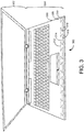
- FIG. 3 illustrates an example portable electronic device 300.
- Electronic device 300 may include a base 304 and a display 302.
- Base 304 may include a keyboard, touch pad and other electronic components, such as processor, battery, memory, mother board and the like.
- Base 304 may include a housing 306 arranged to substantially house the electronic components.
- Example electronic devices 300 may include notebook computers, tablet computers, mobile phones, media players, personal digital assistants (PDAs), and the like.
- PDAs personal digital assistants
- housing 306 may be formed of a first multi-layer structure 308 and a second multi-layer structure 310 attached to first multi-layer structure 308 using an insert molding process.
- First multi-layer structure 308 and second multi-layer structure 310 are described with respect to FIGs. 1 and 2 .
- First multi-layer structure 308 may include a first layer including at least one protruding feature and at least one recessing feature on an edge of first layer.
- First multi-layer structure 308 may include a second layer integrally formed on first layer. As shown in FIG. 3 , inner layer (e.g., first layer) may not be visible once housing is fabricated.
- Second layer may include at least one protruding feature 312 and at least one recessing feature 314 on an edge of second layer.
- Second multi-layer structure 310 may be attached to first multi-layer structure 308 through protruding features and recessing features on the edge of first layer and second layer to provide a bonding force in x, y and z directions.
- the bonding structure may prevent second multi-layer structure (e.g., plastic portion) from moving relative to first multi-layer structure (e.g., metallic body) along an X-axis, a Y-axis, and a Z-axis.
- the bonding structure e.g., zipper structure described herein may improve the bonding strength between the metallic structure and the plastic structure.
- the multi-layer structure (e.g., formed via protruding features 312 and 316 and recessing features 314 and 318) in FIG. 3 may be shown for illustrative purpose and may not be visible upon performing the painting process on the housing 306. Even though FIG. 3 depicts the assembly structure/bonding structure on a top portion of the base, the assembly structure can be applicable for any other portion of the electronic device such as display cover, bottom portion of the base and the like.
Landscapes
- Engineering & Computer Science (AREA)
- Mechanical Engineering (AREA)
- Theoretical Computer Science (AREA)
- Manufacturing & Machinery (AREA)
- General Engineering & Computer Science (AREA)
- Physics & Mathematics (AREA)
- Computer Hardware Design (AREA)
- Human Computer Interaction (AREA)
- General Physics & Mathematics (AREA)
- Microelectronics & Electronic Packaging (AREA)
- Power Engineering (AREA)
- Mathematical Physics (AREA)
- Chemical & Material Sciences (AREA)
- Composite Materials (AREA)
- Casings For Electric Apparatus (AREA)
- Laminated Bodies (AREA)
- Telephone Set Structure (AREA)
Description
- Electronic devices may include a housing for enclosing or securing various device components and circuitry. The characteristics of housings may vary from device to device. For example, housings for computers, phones, and keyboards are generally different, and may be formed using different materials and assembly techniques.
-
US 2011/008566 A1 describes a composite shaped article with an uneven configuration junction face.US 2013/242487 A1 describes a metal composite chassis for electronic equipment.US 2015/366088 A1 describes a composite plate structure having fibre layers. - Examples are described in the following detailed description and in reference to the drawings, in which:
-
FIG. 1A is a perspective view of an example housing depicting a multi-layer structure; -
FIG. 1B depicts a top view of a portion of the example multi-layer structure shown inFIG. 1 ; -
FIG. 1C depicts a bottom view of a portion of the example multi-layer structure shown inFIG. 1 ; -
FIG. 2 depicts a perspective view of an example multi-layer structure assembly; and -
FIG. 3 depicts an example portable electronic device including a housing formed using the multi-layer structure assembly. - Housings for computers, phones, and keyboards may be generally different, and may be formed using different materials and assembly techniques. Housings may be formed of metal and plastic bonding to save cost and to keep the devices lighter. In some electronic devices, housings may be formed of metal and plastic bonding to allow transmission/reception of wireless antenna signals. Despite the variation in construction, some housings may have generally formed from two or more housing parts that are fixed together, which may cause a cosmetic issue (e.g., bonding may gradually fail over time) due to material bonding force between the housing parts lower than external loading. For example, in notebook computers, the cosmetic issue may be caused due to less spacing for insert molding zipper structure between the housing parts, varied cosmetic painting process or high temperatures involved in finishing process.
- Examples described herein may describe a housing for an electronic device, which may include a first multi-layer structure and a second multi-layer structure. In one example, the first multi-layer structure may include a first layer and a second layer formed on the first layer. Each of the first layer and the second layer may include a plurality of protruding features and a plurality of recessing features on an edge of the first multi-layer structure. Example protruding features and recessing features on the first layer and the second layer may be "T" shaped, mushroom shaped, rectangular shaped or a combination thereof.
- In one example, at least one of the recessing features of one layer may intersect at least one of the protruding features of other layer. For example, at least one recessing feature of the first layer may intersect the at least one protruding feature of the second layer. The second multi-layer structure may be bonded to the first multi-layer structure through the plurality of protruding features and the plurality of recessing features on the edge of the first multi-layer structure to provide a bonding force in x, y and z directions,
- The intersecting portion of the first layer and the second layer can help to constrain each of the first layer and the second layer and enhance the bonding force between the first and the second multi-layer structures. The multi-layer structure described herein may also protect against the external load and hence may reduce/overcome the cosmetic issue.
-
FIGs. 1A-1C depict anexample housing 100 depicting amulti-layer structure 102. Particularly,FIG. 1A is a perspective view of anexample housing 100 depicting amulti-layer structure 102.FIG. 1B depicts a top view of a portion of examplemulti-layer structure 102 shown inFIG. 1A .FIG. 1C depicts a bottom view of a portion of examplemulti-layer structure 102 shown inFIG. 1A .Multi-layer structure 102 can, for example, represent a material utilized as housing of the electronic device.Housing 100 may include a firstmulti-layer structure 102. Firstmulti-layer structure 102 may include afirst layer 106 and asecond layer 104 formed onfirst layer 106. For example, different layers of firstmulti-layer structure 102 can be made of different materials (e.g., different metals) or same material. Firstmulti-layer structure 102 that is a portion ofhousing 100 may be a bezel section, a front section, and/or a back section of thehousing 100. -
First layer 106 may include protrudingfeatures 112 and recessingfeatures 114 on an edge offirst layer 106.Second layer 104 may include protrudingfeatures 108 and recessingfeatures 110 on an edge ofsecond layer 104. In one example, at least one of recessing features 114 of one layer (e.g., first layer 106) may intersect (e.g., as shown in intersecting portion 116) at least one of protrudingfeatures 108 of other layer (e.g., second layer 104). In another example, at least some portion of recessingfeatures 114 offirst layer 106 may overlap with at least some portion of protrudingfeatures 108 ofsecond layer 104. Protruding features 108, 112 and recessingfeatures first layer 106 andsecond layer 104 may form a dual-layer zipper structure. In each layer, a recessing feature (e.g., 110, 114) may be formed between two protruding features (e.g., 108, 112) to form a zipper structure. - Further,
housing 100 may include a second multi-layer structure (e.g., 204 as shown inFig. 2 ). In one example, second multi-layer structure may be bonded to firstmulti-layer structure 102 using protruding features 108, 112 and recessingfeatures 110, 1 14 on the edge offirst layer 106 andsecond layer 104. This is explained in detail inFIG. 2 . - Referring now to
FIG. 2 , which depicts a perspective view of an examplemulti-layer structure assembly 200.Assembly 200 may include a firstmulti-layer structure 202 and a secondmulti-layer structure 204 that can be bonded to firstmulti-layer structure 202. Firstmulti-layer structure 202 may include afirst layer 208 and asecond layer 206 integrally formed onfirst layer 208.First layer 208 andsecond layer 206 may be metal layers that are laminated together.First layer 208 andsecond layer 206 can utilize different metals. Firstmulti-layer structure 202 may be made by metal manufacturing methods such as compression molding, casting, pressing forming, forging, and punching. - Each of
first layer 208 andsecond layer 206 may include at least oneprotruding feature feature multi-layer structure 202. Protruding features 214 offirst layer 208 may be substantially offset from protrudingfeatures 210 ofsecond layer 206 and recessingfeatures 216 offirst layer 208 may be substantially offset from recessingfeatures 212 ofsecond layer 206. In one example, recessingfeatures 216 of one layer (e.g., first layer 208) may intersect (e.g., as shown in intersecting portion 218) protrudingfeatures 210 of other layer (e.g., second layer 206). - Second
multi-layer structure 204 may be bonded to firstmulti-layer structure 202 via protruding features 210, 214 and recessing features 212, 216 on the edge of firstmulti-layer structure 202 to provide a bonding force. In one example, secondmulti-layer structure 204 may be insert molded onto protruding features 210, 214 and recessing features 212, 216 on edge of firstmulti-layer structure 202. Firstmulti-layer structure 202 and secondmulti-layer structure 204 may be joined together without gaps. For example, in insert molding process, metallic multi-layer structure (e.g., 202) may accept the flow of melted plastic multi-layer structure (e.g., 204) into recessing features and the plastic may be hardened white the melted plastic multi-layer structure is inside the recessing features, thereby attaching the plastic multi-layer structure to the metallic multi-layer structure. Examples for attaching first and second multi-layer structures may not be limited to insert molding and any other process (e.g., Ultrasonic bonding) may be used for attaching first and second multi-layer structures such that first and second multi-layer structures may form a housing for electronic device. - For example, second
multi-layer structure 204 may include a first andsecond layers second layers multi-layer structure 204 may be disposed within the corresponding recessing features 212, 216 of firstmulti-layer structure 202. Similarly, protruding features 210, 214 of firstmulti-layer structure 202 may be disposed within the corresponding recessing features (e.g., 222) offirst layer 226 and thesecond layer 228 of secondmulti-layer structure 204. In the example shown inFIG. 2 , the recessing features of inner layer (e.g., first layer 226) may not be visible. - First
multi-layer structure 202 and secondmulti-layer structure 204 may be made up of a same material or a different material. In one example, firstmulti-layer structure 202 may be made up of a metallic material and secondmulti-layer structure 204 may be made up of a plastic material. For example, firstmulti-layer structure 202 may be made up of a metallic material selected from a group consisting of aluminum, magnesium, zinc, titanium, aluminum alloy, magnesium alloy, zinc alloy, and titanium alloy. Secondmulti-layer structure 204 may be made up of a plastic material selected from a group consisting of liquid crystal polymer, polyphenylene sulphide, and poly butylene terephthalate. Also, material of secondmulti-layer structure 204 can be selected to have a good bonding ability with material of firstmulti-layer structure 202. For example, the plastic portion may substantially an elongated portion adjacent to one edge of the metallic body. The plastic portion may be made of a material which can be able to firmly bond with the metallic body, for example, a material with relatively low shrinkage and a linear expansion coefficient substantially equal to that of the metallic material of firstmulti-layer structure 202. For instance, protruding features (e.g., 210, 214) that extend from the edge of the metal part may allow the moldable plastic material to adhere to the protruding features, hence, may have an increased binding area that allows the moldable plastic material to bind to the metal part. Even though the examples inFIGs. 1 and2 may describe the multi-layer structure as including two layers, the multi-layer structure can include more than two layers. - Further, painting process may be performed on the first and second
multi-layer structures -
FIG. 3 illustrates an example portableelectronic device 300.Electronic device 300 may include abase 304 and adisplay 302.Base 304 may include a keyboard, touch pad and other electronic components, such as processor, battery, memory, mother board and the like.Base 304 may include ahousing 306 arranged to substantially house the electronic components. Exampleelectronic devices 300 may include notebook computers, tablet computers, mobile phones, media players, personal digital assistants (PDAs), and the like. - In one example,
housing 306 may be formed of a firstmulti-layer structure 308 and a secondmulti-layer structure 310 attached to firstmulti-layer structure 308 using an insert molding process. Firstmulti-layer structure 308 and secondmulti-layer structure 310 are described with respect toFIGs. 1 and2 . Firstmulti-layer structure 308 may include a first layer including at least one protruding feature and at least one recessing feature on an edge of first layer. Firstmulti-layer structure 308 may include a second layer integrally formed on first layer. As shown inFIG. 3 , inner layer (e.g., first layer) may not be visible once housing is fabricated. Second layer may include at least one protrudingfeature 312 and at least onerecessing feature 314 on an edge of second layer. Recessing features of first layer may intersect/overlap protruding features 312 of second layer. Secondmulti-layer structure 310 may be attached to firstmulti-layer structure 308 through protruding features and recessing features on the edge of first layer and second layer to provide a bonding force in x, y and z directions. For example, the bonding structure may prevent second multi-layer structure (e.g., plastic portion) from moving relative to first multi-layer structure (e.g., metallic body) along an X-axis, a Y-axis, and a Z-axis. For example, the bonding structure (e.g., zipper structure) described herein may improve the bonding strength between the metallic structure and the plastic structure. For example, the multi-layer structure (e.g., formed via protruding features 312 and 316 and recessingfeatures 314 and 318) inFIG. 3 may be shown for illustrative purpose and may not be visible upon performing the painting process on thehousing 306. Even thoughFIG. 3 depicts the assembly structure/bonding structure on a top portion of the base, the assembly structure can be applicable for any other portion of the electronic device such as display cover, bottom portion of the base and the like. - It may be noted that the above-described examples of the present solution is for the purpose of illustration only. Although the solution has been described in conjunction with a specific embodiment thereof, numerous modifications may be possible without materially departing from the teachings and advantages of the subject matter described herein. Other substitutions, modifications and changes may be made without departing from the spirit of the present solution. All of the features disclosed in this specification (including any accompanying claims, abstract and drawings), and/or all of the steps of any method or process so disclosed, may be combined in any combination, except combinations where at least some of such features and/or steps are mutually exclusive.
- The terms "include," "have," and variations thereof, as used herein, have the same meaning as the term "comprise" or appropriate variation thereof. Furthermore, the term "based on," as used herein, means "based at least in part on." Thus, a feature that is described as based on some stimulus can be based on the stimulus or a combination of stimuli including the stimulus.
- The present description has been shown and described with reference to the foregoing examples, It is understood, however, that other forms, details, and examples can be made without departing from the scope of the present invention as defined in the independent claim. Preferred embodiments are defined in the dependent claims.
Claims (15)
- A housing (100, 306) for an electronic device (300) comprising:a first multi-layer structure (102, 202, 308) comprising:a first layer (106, 208); anda second layer (104, 206) formed on the first layer (106, 208),wherein each of the first layer (106, 208) and the second layer (104, 206) comprises a plurality of protruding features (108, 112, 210, 214, 312) and a plurality of recessing features (110, 114, 212, 216, 318) on an edge of the first layer (106, 208) and the second layer (104, 206), wherein at least one of the plurality of recessing features (110, 114, 212, 216, 318) of one layer intersects at least one of the plurality of protruding features (108, 112, 210, 214, 312) of the other layer.
- The housing (100, 306) of claim 1, further comprising:
a second multi-layer structure (204, 310) bonded to the first multi-layer structure (102, 202, 308) using the plurality of protruding features (108, 112, 210, 214, 312) and the plurality of recessing features (110, 114, 212, 216, 318) on the edge of the first layer (106, 208) and the second layer (104, 206). - The housing (100, 306) of claim 2, wherein the first multi-layer structure (102, 202, 308) and the second multi-layer structure (204, 310) are made up of a same material or a different material.
- The housing (100, 306) of claim 2, wherein the second multi-layer structure (204, 310) is made up of a plastic material selected from a group consisting of liquid crystal polymer, polyphenylene sulphide, and poly butylene terephthalate.
- The housing (100, 306) of claim 1, wherein the first multi-layer structure (102, 202, 308) is made up of a metallic material selected from a group consisting of aluminum, magnesium, zinc, titanium, aluminum alloy, magnesium alloy, zinc alloy, and titanium alloy.
- The housing (100, 306) of claim 1, wherein the plurality of protruding features (108, 112, 210, 214, 312) and the plurality of recessing features (110, 114, 212, 216, 318) of the first layer (106, 208) and the second layer (104, 206) form a dual-layer zipper structure.
- A housing as claimed in claim 1, wherein the second layer is formed integrally on the first layer, and further comprising:
a second multi-layer structure (204, 310) bonded to the first multi-layer structure (102, 202, 308) via the plurality of protruding features (108, 112, 210, 214, 312) and the plurality of recessing features (110, 114, 212, 216, 318) on the edge of the first multi-layer structure (102, 202, 308) to provide a bonding force. - The housing of claim 7, wherein the second multi-layer structure (204, 310) is insert molded onto the plurality of protruding features (108, 112, 210, 214, 312) and the plurality of recessing features (110, 114, 212, 216, 318) on the edge of the first multi-layer structure (102, 202, 308).
- The housing of claim 7, wherein the first multi-layer structure (102, 202, 308) is made up of a metallic material.
- The housing of claim 7, wherein the second multi-layer structure (204, 310) is made up of a plastic material.
- The housing of claim 7, wherein the plurality of protruding features (108, 112, 210, 214, 312) of the first layer (106, 208) are substantially offset from the plurality of protruding features (108, 112, 210, 214, 312) of the second layer (104, 206).
- The housing of claim 7, wherein the plurality of recessing features (110, 114, 212, 216, 318) of the first layer (106, 208) are substantially offset from the plurality of recessing features (110, 114, 212, 216, 318) of the second layer (104, 206).
- A portable electronic device (300), comprising:at least one electronic component; andthe housing (100, 306) claimed in claim 1, wherein the second layer is formed integrally on the first layer, and wherein the housing is arranged to substantially house the at least one electronic component.
- The portable electronic device (300) of claim 13, wherein the housing (100, 306) comprises:
a second multi-layer structure (204, 310) attached to the first multi-layer structure (102, 202, 308) through the plurality of protruding features (108, 112, 210, 214, 312) and the plurality of recessing features (110, 114, 212, 216, 318) on the edge of the first layer (106, 208) and the second layer (104, 206) to provide a bonding force in x, y and z directions. - The portable electronic device (300) of claim 13, wherein the plurality of protruding features (108, 112, 210, 214, 312) of the first layer (106, 208) are substantially offset from the plurality of protruding features (108, 112, 210, 214, 312) of the second layer (104, 206), and wherein the plurality of recessing features (110, 114, 212, 216, 318) of the first layer (106, 208) are substantially offset from the plurality of recessing features (110, 114, 212, 216, 318) of the second layer (104, 206).
Applications Claiming Priority (1)
| Application Number | Priority Date | Filing Date | Title |
|---|---|---|---|
| PCT/US2016/025951 WO2017176250A1 (en) | 2016-04-05 | 2016-04-05 | Multilayer structures for electronic device housings |
Publications (3)
| Publication Number | Publication Date |
|---|---|
| EP3439863A1 EP3439863A1 (en) | 2019-02-13 |
| EP3439863A4 EP3439863A4 (en) | 2019-11-13 |
| EP3439863B1 true EP3439863B1 (en) | 2021-03-03 |
Family
ID=60000588
Family Applications (1)
| Application Number | Title | Priority Date | Filing Date |
|---|---|---|---|
| EP16898095.1A Not-in-force EP3439863B1 (en) | 2016-04-05 | 2016-04-05 | Multilayer structures for electronic device housings |
Country Status (5)
| Country | Link |
|---|---|
| US (1) | US10543657B2 (en) |
| EP (1) | EP3439863B1 (en) |
| CN (1) | CN108602299B (en) |
| TW (1) | TWI630859B (en) |
| WO (1) | WO2017176250A1 (en) |
Family Cites Families (17)
| Publication number | Priority date | Publication date | Assignee | Title |
|---|---|---|---|---|
| US5354951A (en) * | 1993-03-15 | 1994-10-11 | Leader Tech, Inc. | Circuit board component shielding enclosure and assembly |
| US6313400B1 (en) * | 1999-07-13 | 2001-11-06 | Itt Manufacturing Enterprises, Inc. | Data card easily assembled housing |
| JP2002043785A (en) * | 2000-07-28 | 2002-02-08 | Murata Mfg Co Ltd | Shielding case, electronic device using the same, electronic apparatus using the same, and method of manufacturing the same |
| US6574096B1 (en) | 2000-09-29 | 2003-06-03 | Apple Computer, Inc. | Use of titanium in a notebook computer |
| US9345183B2 (en) * | 2005-03-15 | 2016-05-17 | Stealthdrive Canada Corp. | EMI-shielding solutions for electronics enclosures using opposing three-dimensional shapes and channels formed in sheet metal |
| ES2397240T3 (en) * | 2007-09-11 | 2013-03-05 | Toray Industries, Inc. | Composed article of composite material and process to manufacture it |
| US20100238621A1 (en) | 2009-03-20 | 2010-09-23 | Tracy Mark S | Insert-molded conductor |
| EP2647486B1 (en) | 2010-12-02 | 2016-06-01 | Toray Industries, Inc. | Method for producing metal composite, and chassis for electronic equipment |
| US8927881B2 (en) | 2012-09-07 | 2015-01-06 | Apple Inc. | Insert molded cowling structures |
| US8718731B1 (en) * | 2013-01-30 | 2014-05-06 | Wai Tang | Shock-absorbent electronic device case |
| US20160174420A1 (en) * | 2013-03-15 | 2016-06-16 | Paul Douglas Cochrane | Formed channels providing electromagnetic shielding in electronics |
| US8861191B1 (en) | 2013-09-30 | 2014-10-14 | Google Inc. | Apparatus related to a structure of a base portion of a computing device |
| KR20160129007A (en) | 2014-03-04 | 2016-11-08 | 엠씨10, 인크 | Multi-part flexible encapsulation housing for electronic devices |
| TWI562895B (en) | 2014-06-11 | 2016-12-21 | Compal Electronics Inc | Composite plate structure and manufacturing method thereof |
| US9232031B1 (en) | 2014-06-11 | 2016-01-05 | Amazon Technologies, Inc. | Computing device components and assembly |
| US9690331B2 (en) | 2014-08-18 | 2017-06-27 | Beijing Lenovo Software Ltd. | Electronic apparatus and method for producing housing thereof |
| CN104320931A (en) * | 2014-11-03 | 2015-01-28 | 联想(北京)有限公司 | Electronic device and method for manufacturing shell of electronic device |
-
2016
- 2016-04-05 US US16/067,729 patent/US10543657B2/en not_active Expired - Fee Related
- 2016-04-05 EP EP16898095.1A patent/EP3439863B1/en not_active Not-in-force
- 2016-04-05 CN CN201680079304.9A patent/CN108602299B/en not_active Expired - Fee Related
- 2016-04-05 WO PCT/US2016/025951 patent/WO2017176250A1/en not_active Ceased
-
2017
- 2017-03-10 TW TW106107975A patent/TWI630859B/en not_active IP Right Cessation
Non-Patent Citations (1)
| Title |
|---|
| None * |
Also Published As
| Publication number | Publication date |
|---|---|
| TW201740782A (en) | 2017-11-16 |
| US20190016082A1 (en) | 2019-01-17 |
| CN108602299A (en) | 2018-09-28 |
| EP3439863A1 (en) | 2019-02-13 |
| EP3439863A4 (en) | 2019-11-13 |
| WO2017176250A1 (en) | 2017-10-12 |
| US10543657B2 (en) | 2020-01-28 |
| CN108602299B (en) | 2020-06-26 |
| TWI630859B (en) | 2018-07-21 |
Similar Documents
| Publication | Publication Date | Title |
|---|---|---|
| US9894787B2 (en) | Systems and methods for coupling sections of an electronic device | |
| US8646637B2 (en) | Perforated substrates for forming housings | |
| US10361479B2 (en) | Portable electronic device housing having insert molding around antenna | |
| EP3376336B1 (en) | Electronic device housing, electronic device comprising said electronic device housing and method of assembling said electronic device | |
| CN206698539U (en) | Housings for electronic devices and electronic devices | |
| KR102246134B1 (en) | Electronic device and protection cover thereof | |
| KR20240135075A (en) | Device enclosure | |
| US20130170159A1 (en) | Housing for portable electronic devices | |
| US10606218B1 (en) | Ceramic weave for low-cost, structural, antenna-permeable watch case | |
| JP2009266195A (en) | Casing for electronic device, and method for manufacturing the same | |
| US20180206330A1 (en) | Electromagnetic shielding protection film and fpc | |
| CN111491469B (en) | Core-shell with various filler materials for enhanced thermal conductivity | |
| US9755297B2 (en) | Housing, electronic device using same, and method for making same | |
| CN205736007U (en) | Shell and electronic equipment | |
| US20200307145A1 (en) | Functional composite enclosure for an electronic device | |
| US10543657B2 (en) | Multilayer structures for electronic device housings | |
| JP2018160538A (en) | Electronics | |
| US8628836B2 (en) | Method and apparatus for bonding metals and composites | |
| CN211429795U (en) | Shell assembly and electronic device | |
| TWI635524B (en) | Keyboard housing structure having a reinforced supporting plate portion | |
| KR101576155B1 (en) | Magnetic Shielding Sheet and Portable Terminal having the same | |
| CN223024745U (en) | Circuit board assembly and electronic equipment | |
| WO2017120715A1 (en) | Display cover for electronic devices | |
| CN201741412U (en) | Combination structure of electronic product metal case and plastic connector | |
| US20220129039A1 (en) | Electronic device housings with shock absorbers |
Legal Events
| Date | Code | Title | Description |
|---|---|---|---|
| STAA | Information on the status of an ep patent application or granted ep patent |
Free format text: STATUS: THE INTERNATIONAL PUBLICATION HAS BEEN MADE |
|
| PUAI | Public reference made under article 153(3) epc to a published international application that has entered the european phase |
Free format text: ORIGINAL CODE: 0009012 |
|
| STAA | Information on the status of an ep patent application or granted ep patent |
Free format text: STATUS: REQUEST FOR EXAMINATION WAS MADE |
|
| 17P | Request for examination filed |
Effective date: 20180713 |
|
| AK | Designated contracting states |
Kind code of ref document: A1 Designated state(s): AL AT BE BG CH CY CZ DE DK EE ES FI FR GB GR HR HU IE IS IT LI LT LU LV MC MK MT NL NO PL PT RO RS SE SI SK SM TR |
|
| AX | Request for extension of the european patent |
Extension state: BA ME |
|
| RAP1 | Party data changed (applicant data changed or rights of an application transferred) |
Owner name: HEWLETT-PACKARD DEVELOPMENT COMPANY, L.P. |
|
| DAV | Request for validation of the european patent (deleted) | ||
| DAX | Request for extension of the european patent (deleted) | ||
| A4 | Supplementary search report drawn up and despatched |
Effective date: 20191015 |
|
| RIC1 | Information provided on ipc code assigned before grant |
Ipc: B32B 3/06 20060101AFI20191009BHEP Ipc: B29C 70/68 20060101ALI20191009BHEP Ipc: B29C 45/14 20060101ALI20191009BHEP Ipc: H05K 5/00 20060101ALI20191009BHEP |
|
| GRAP | Despatch of communication of intention to grant a patent |
Free format text: ORIGINAL CODE: EPIDOSNIGR1 |
|
| STAA | Information on the status of an ep patent application or granted ep patent |
Free format text: STATUS: GRANT OF PATENT IS INTENDED |
|
| RIC1 | Information provided on ipc code assigned before grant |
Ipc: B29C 45/14 20060101ALI20200814BHEP Ipc: B32B 3/06 20060101AFI20200814BHEP Ipc: B29C 70/68 20060101ALI20200814BHEP Ipc: H05K 5/00 20060101ALI20200814BHEP |
|
| INTG | Intention to grant announced |
Effective date: 20200921 |
|
| GRAS | Grant fee paid |
Free format text: ORIGINAL CODE: EPIDOSNIGR3 |
|
| GRAA | (expected) grant |
Free format text: ORIGINAL CODE: 0009210 |
|
| STAA | Information on the status of an ep patent application or granted ep patent |
Free format text: STATUS: THE PATENT HAS BEEN GRANTED |
|
| AK | Designated contracting states |
Kind code of ref document: B1 Designated state(s): AL AT BE BG CH CY CZ DE DK EE ES FI FR GB GR HR HU IE IS IT LI LT LU LV MC MK MT NL NO PL PT RO RS SE SI SK SM TR |
|
| REG | Reference to a national code |
Ref country code: GB Ref legal event code: FG4D |
|
| REG | Reference to a national code |
Ref country code: AT Ref legal event code: REF Ref document number: 1366755 Country of ref document: AT Kind code of ref document: T Effective date: 20210315 Ref country code: CH Ref legal event code: EP |
|
| REG | Reference to a national code |
Ref country code: DE Ref legal event code: R096 Ref document number: 602016053823 Country of ref document: DE |
|
| REG | Reference to a national code |
Ref country code: IE Ref legal event code: FG4D |
|
| REG | Reference to a national code |
Ref country code: LT Ref legal event code: MG9D |
|
| PG25 | Lapsed in a contracting state [announced via postgrant information from national office to epo] |
Ref country code: GR Free format text: LAPSE BECAUSE OF FAILURE TO SUBMIT A TRANSLATION OF THE DESCRIPTION OR TO PAY THE FEE WITHIN THE PRESCRIBED TIME-LIMIT Effective date: 20210604 Ref country code: FI Free format text: LAPSE BECAUSE OF FAILURE TO SUBMIT A TRANSLATION OF THE DESCRIPTION OR TO PAY THE FEE WITHIN THE PRESCRIBED TIME-LIMIT Effective date: 20210303 Ref country code: HR Free format text: LAPSE BECAUSE OF FAILURE TO SUBMIT A TRANSLATION OF THE DESCRIPTION OR TO PAY THE FEE WITHIN THE PRESCRIBED TIME-LIMIT Effective date: 20210303 Ref country code: NO Free format text: LAPSE BECAUSE OF FAILURE TO SUBMIT A TRANSLATION OF THE DESCRIPTION OR TO PAY THE FEE WITHIN THE PRESCRIBED TIME-LIMIT Effective date: 20210603 Ref country code: BG Free format text: LAPSE BECAUSE OF FAILURE TO SUBMIT A TRANSLATION OF THE DESCRIPTION OR TO PAY THE FEE WITHIN THE PRESCRIBED TIME-LIMIT Effective date: 20210603 Ref country code: LT Free format text: LAPSE BECAUSE OF FAILURE TO SUBMIT A TRANSLATION OF THE DESCRIPTION OR TO PAY THE FEE WITHIN THE PRESCRIBED TIME-LIMIT Effective date: 20210303 |
|
| REG | Reference to a national code |
Ref country code: NL Ref legal event code: MP Effective date: 20210303 |
|
| REG | Reference to a national code |
Ref country code: AT Ref legal event code: MK05 Ref document number: 1366755 Country of ref document: AT Kind code of ref document: T Effective date: 20210303 |
|
| PG25 | Lapsed in a contracting state [announced via postgrant information from national office to epo] |
Ref country code: RS Free format text: LAPSE BECAUSE OF FAILURE TO SUBMIT A TRANSLATION OF THE DESCRIPTION OR TO PAY THE FEE WITHIN THE PRESCRIBED TIME-LIMIT Effective date: 20210303 Ref country code: LV Free format text: LAPSE BECAUSE OF FAILURE TO SUBMIT A TRANSLATION OF THE DESCRIPTION OR TO PAY THE FEE WITHIN THE PRESCRIBED TIME-LIMIT Effective date: 20210303 Ref country code: PL Free format text: LAPSE BECAUSE OF FAILURE TO SUBMIT A TRANSLATION OF THE DESCRIPTION OR TO PAY THE FEE WITHIN THE PRESCRIBED TIME-LIMIT Effective date: 20210303 Ref country code: SE Free format text: LAPSE BECAUSE OF FAILURE TO SUBMIT A TRANSLATION OF THE DESCRIPTION OR TO PAY THE FEE WITHIN THE PRESCRIBED TIME-LIMIT Effective date: 20210303 |
|
| PG25 | Lapsed in a contracting state [announced via postgrant information from national office to epo] |
Ref country code: NL Free format text: LAPSE BECAUSE OF FAILURE TO SUBMIT A TRANSLATION OF THE DESCRIPTION OR TO PAY THE FEE WITHIN THE PRESCRIBED TIME-LIMIT Effective date: 20210303 |
|
| PG25 | Lapsed in a contracting state [announced via postgrant information from national office to epo] |
Ref country code: AT Free format text: LAPSE BECAUSE OF FAILURE TO SUBMIT A TRANSLATION OF THE DESCRIPTION OR TO PAY THE FEE WITHIN THE PRESCRIBED TIME-LIMIT Effective date: 20210303 Ref country code: SM Free format text: LAPSE BECAUSE OF FAILURE TO SUBMIT A TRANSLATION OF THE DESCRIPTION OR TO PAY THE FEE WITHIN THE PRESCRIBED TIME-LIMIT Effective date: 20210303 Ref country code: EE Free format text: LAPSE BECAUSE OF FAILURE TO SUBMIT A TRANSLATION OF THE DESCRIPTION OR TO PAY THE FEE WITHIN THE PRESCRIBED TIME-LIMIT Effective date: 20210303 Ref country code: CZ Free format text: LAPSE BECAUSE OF FAILURE TO SUBMIT A TRANSLATION OF THE DESCRIPTION OR TO PAY THE FEE WITHIN THE PRESCRIBED TIME-LIMIT Effective date: 20210303 |
|
| PG25 | Lapsed in a contracting state [announced via postgrant information from national office to epo] |
Ref country code: IS Free format text: LAPSE BECAUSE OF FAILURE TO SUBMIT A TRANSLATION OF THE DESCRIPTION OR TO PAY THE FEE WITHIN THE PRESCRIBED TIME-LIMIT Effective date: 20210703 Ref country code: SK Free format text: LAPSE BECAUSE OF FAILURE TO SUBMIT A TRANSLATION OF THE DESCRIPTION OR TO PAY THE FEE WITHIN THE PRESCRIBED TIME-LIMIT Effective date: 20210303 Ref country code: RO Free format text: LAPSE BECAUSE OF FAILURE TO SUBMIT A TRANSLATION OF THE DESCRIPTION OR TO PAY THE FEE WITHIN THE PRESCRIBED TIME-LIMIT Effective date: 20210303 Ref country code: PT Free format text: LAPSE BECAUSE OF FAILURE TO SUBMIT A TRANSLATION OF THE DESCRIPTION OR TO PAY THE FEE WITHIN THE PRESCRIBED TIME-LIMIT Effective date: 20210705 |
|
| REG | Reference to a national code |
Ref country code: DE Ref legal event code: R097 Ref document number: 602016053823 Country of ref document: DE |
|
| PG25 | Lapsed in a contracting state [announced via postgrant information from national office to epo] |
Ref country code: LU Free format text: LAPSE BECAUSE OF NON-PAYMENT OF DUE FEES Effective date: 20210405 |
|
| PLBE | No opposition filed within time limit |
Free format text: ORIGINAL CODE: 0009261 |
|
| STAA | Information on the status of an ep patent application or granted ep patent |
Free format text: STATUS: NO OPPOSITION FILED WITHIN TIME LIMIT |
|
| REG | Reference to a national code |
Ref country code: BE Ref legal event code: MM Effective date: 20210430 |
|
| PG25 | Lapsed in a contracting state [announced via postgrant information from national office to epo] |
Ref country code: ES Free format text: LAPSE BECAUSE OF FAILURE TO SUBMIT A TRANSLATION OF THE DESCRIPTION OR TO PAY THE FEE WITHIN THE PRESCRIBED TIME-LIMIT Effective date: 20210303 Ref country code: MC Free format text: LAPSE BECAUSE OF FAILURE TO SUBMIT A TRANSLATION OF THE DESCRIPTION OR TO PAY THE FEE WITHIN THE PRESCRIBED TIME-LIMIT Effective date: 20210303 Ref country code: LI Free format text: LAPSE BECAUSE OF NON-PAYMENT OF DUE FEES Effective date: 20210430 Ref country code: DK Free format text: LAPSE BECAUSE OF FAILURE TO SUBMIT A TRANSLATION OF THE DESCRIPTION OR TO PAY THE FEE WITHIN THE PRESCRIBED TIME-LIMIT Effective date: 20210303 Ref country code: CH Free format text: LAPSE BECAUSE OF NON-PAYMENT OF DUE FEES Effective date: 20210430 Ref country code: AL Free format text: LAPSE BECAUSE OF FAILURE TO SUBMIT A TRANSLATION OF THE DESCRIPTION OR TO PAY THE FEE WITHIN THE PRESCRIBED TIME-LIMIT Effective date: 20210303 |
|
| 26N | No opposition filed |
Effective date: 20211206 |
|
| PG25 | Lapsed in a contracting state [announced via postgrant information from national office to epo] |
Ref country code: SI Free format text: LAPSE BECAUSE OF FAILURE TO SUBMIT A TRANSLATION OF THE DESCRIPTION OR TO PAY THE FEE WITHIN THE PRESCRIBED TIME-LIMIT Effective date: 20210303 |
|
| PG25 | Lapsed in a contracting state [announced via postgrant information from national office to epo] |
Ref country code: IT Free format text: LAPSE BECAUSE OF FAILURE TO SUBMIT A TRANSLATION OF THE DESCRIPTION OR TO PAY THE FEE WITHIN THE PRESCRIBED TIME-LIMIT Effective date: 20210303 Ref country code: IE Free format text: LAPSE BECAUSE OF NON-PAYMENT OF DUE FEES Effective date: 20210405 |
|
| PGFP | Annual fee paid to national office [announced via postgrant information from national office to epo] |
Ref country code: GB Payment date: 20220323 Year of fee payment: 7 |
|
| PG25 | Lapsed in a contracting state [announced via postgrant information from national office to epo] |
Ref country code: IS Free format text: LAPSE BECAUSE OF FAILURE TO SUBMIT A TRANSLATION OF THE DESCRIPTION OR TO PAY THE FEE WITHIN THE PRESCRIBED TIME-LIMIT Effective date: 20210703 |
|
| PGFP | Annual fee paid to national office [announced via postgrant information from national office to epo] |
Ref country code: FR Payment date: 20220323 Year of fee payment: 7 |
|
| PG25 | Lapsed in a contracting state [announced via postgrant information from national office to epo] |
Ref country code: BE Free format text: LAPSE BECAUSE OF NON-PAYMENT OF DUE FEES Effective date: 20210430 |
|
| PGFP | Annual fee paid to national office [announced via postgrant information from national office to epo] |
Ref country code: DE Payment date: 20220322 Year of fee payment: 7 |
|
| PG25 | Lapsed in a contracting state [announced via postgrant information from national office to epo] |
Ref country code: CY Free format text: LAPSE BECAUSE OF FAILURE TO SUBMIT A TRANSLATION OF THE DESCRIPTION OR TO PAY THE FEE WITHIN THE PRESCRIBED TIME-LIMIT Effective date: 20210303 |
|
| PG25 | Lapsed in a contracting state [announced via postgrant information from national office to epo] |
Ref country code: HU Free format text: LAPSE BECAUSE OF FAILURE TO SUBMIT A TRANSLATION OF THE DESCRIPTION OR TO PAY THE FEE WITHIN THE PRESCRIBED TIME-LIMIT; INVALID AB INITIO Effective date: 20160405 |
|
| REG | Reference to a national code |
Ref country code: DE Ref legal event code: R119 Ref document number: 602016053823 Country of ref document: DE |
|
| GBPC | Gb: european patent ceased through non-payment of renewal fee |
Effective date: 20230405 |
|
| PG25 | Lapsed in a contracting state [announced via postgrant information from national office to epo] |
Ref country code: GB Free format text: LAPSE BECAUSE OF NON-PAYMENT OF DUE FEES Effective date: 20230405 |
|
| PG25 | Lapsed in a contracting state [announced via postgrant information from national office to epo] |
Ref country code: GB Free format text: LAPSE BECAUSE OF NON-PAYMENT OF DUE FEES Effective date: 20230405 Ref country code: FR Free format text: LAPSE BECAUSE OF NON-PAYMENT OF DUE FEES Effective date: 20230430 Ref country code: DE Free format text: LAPSE BECAUSE OF NON-PAYMENT OF DUE FEES Effective date: 20231103 |
|
| PG25 | Lapsed in a contracting state [announced via postgrant information from national office to epo] |
Ref country code: MK Free format text: LAPSE BECAUSE OF FAILURE TO SUBMIT A TRANSLATION OF THE DESCRIPTION OR TO PAY THE FEE WITHIN THE PRESCRIBED TIME-LIMIT Effective date: 20210303 |
|
| PG25 | Lapsed in a contracting state [announced via postgrant information from national office to epo] |
Ref country code: TR Free format text: LAPSE BECAUSE OF FAILURE TO SUBMIT A TRANSLATION OF THE DESCRIPTION OR TO PAY THE FEE WITHIN THE PRESCRIBED TIME-LIMIT Effective date: 20210303 |
|
| PG25 | Lapsed in a contracting state [announced via postgrant information from national office to epo] |
Ref country code: MT Free format text: LAPSE BECAUSE OF FAILURE TO SUBMIT A TRANSLATION OF THE DESCRIPTION OR TO PAY THE FEE WITHIN THE PRESCRIBED TIME-LIMIT Effective date: 20210303 |