EP3438543A1 - Surge suppression circuit and microwave oven - Google Patents
Surge suppression circuit and microwave oven Download PDFInfo
- Publication number
- EP3438543A1 EP3438543A1 EP16896218.1A EP16896218A EP3438543A1 EP 3438543 A1 EP3438543 A1 EP 3438543A1 EP 16896218 A EP16896218 A EP 16896218A EP 3438543 A1 EP3438543 A1 EP 3438543A1
- Authority
- EP
- European Patent Office
- Prior art keywords
- coupled
- rectifying
- suppression circuit
- capacitor
- surge suppression
- Prior art date
- Legal status (The legal status is an assumption and is not a legal conclusion. Google has not performed a legal analysis and makes no representation as to the accuracy of the status listed.)
- Granted
Links
Images



Classifications
-
- H—ELECTRICITY
- H02—GENERATION; CONVERSION OR DISTRIBUTION OF ELECTRIC POWER
- H02H—EMERGENCY PROTECTIVE CIRCUIT ARRANGEMENTS
- H02H9/00—Emergency protective circuit arrangements for limiting excess current or voltage without disconnection
- H02H9/04—Emergency protective circuit arrangements for limiting excess current or voltage without disconnection responsive to excess voltage
-
- H—ELECTRICITY
- H02—GENERATION; CONVERSION OR DISTRIBUTION OF ELECTRIC POWER
- H02M—APPARATUS FOR CONVERSION BETWEEN AC AND AC, BETWEEN AC AND DC, OR BETWEEN DC AND DC, AND FOR USE WITH MAINS OR SIMILAR POWER SUPPLY SYSTEMS; CONVERSION OF DC OR AC INPUT POWER INTO SURGE OUTPUT POWER; CONTROL OR REGULATION THEREOF
- H02M7/00—Conversion of AC power input into DC power output; Conversion of DC power input into AC power output
- H02M7/02—Conversion of AC power input into DC power output without possibility of reversal
- H02M7/04—Conversion of AC power input into DC power output without possibility of reversal by static converters
- H02M7/06—Conversion of AC power input into DC power output without possibility of reversal by static converters using discharge tubes without control electrode or semiconductor devices without control electrode
- H02M7/062—Avoiding or suppressing excessive transient voltages or currents
-
- F—MECHANICAL ENGINEERING; LIGHTING; HEATING; WEAPONS; BLASTING
- F24—HEATING; RANGES; VENTILATING
- F24C—DOMESTIC STOVES OR RANGES ; DETAILS OF DOMESTIC STOVES OR RANGES, OF GENERAL APPLICATION
- F24C7/00—Stoves or ranges heated by electric energy
- F24C7/02—Stoves or ranges heated by electric energy using microwaves
-
- F—MECHANICAL ENGINEERING; LIGHTING; HEATING; WEAPONS; BLASTING
- F24—HEATING; RANGES; VENTILATING
- F24C—DOMESTIC STOVES OR RANGES ; DETAILS OF DOMESTIC STOVES OR RANGES, OF GENERAL APPLICATION
- F24C7/00—Stoves or ranges heated by electric energy
- F24C7/08—Arrangement or mounting of control or safety devices
-
- F—MECHANICAL ENGINEERING; LIGHTING; HEATING; WEAPONS; BLASTING
- F24—HEATING; RANGES; VENTILATING
- F24C—DOMESTIC STOVES OR RANGES ; DETAILS OF DOMESTIC STOVES OR RANGES, OF GENERAL APPLICATION
- F24C7/00—Stoves or ranges heated by electric energy
- F24C7/08—Arrangement or mounting of control or safety devices
- F24C7/082—Arrangement or mounting of control or safety devices on ranges, e.g. control panels, illumination
-
- H—ELECTRICITY
- H02—GENERATION; CONVERSION OR DISTRIBUTION OF ELECTRIC POWER
- H02H—EMERGENCY PROTECTIVE CIRCUIT ARRANGEMENTS
- H02H7/00—Emergency protective circuit arrangements specially adapted for specific types of electric machines or apparatus or for sectionalised protection of cable or line systems, and effecting automatic switching in the event of an undesired change from normal working conditions
- H02H7/10—Emergency protective circuit arrangements specially adapted for specific types of electric machines or apparatus or for sectionalised protection of cable or line systems, and effecting automatic switching in the event of an undesired change from normal working conditions for converters; for rectifiers
- H02H7/12—Emergency protective circuit arrangements specially adapted for specific types of electric machines or apparatus or for sectionalised protection of cable or line systems, and effecting automatic switching in the event of an undesired change from normal working conditions for converters; for rectifiers for static converters or rectifiers
- H02H7/125—Emergency protective circuit arrangements specially adapted for specific types of electric machines or apparatus or for sectionalised protection of cable or line systems, and effecting automatic switching in the event of an undesired change from normal working conditions for converters; for rectifiers for static converters or rectifiers for rectifiers
- H02H7/1252—Emergency protective circuit arrangements specially adapted for specific types of electric machines or apparatus or for sectionalised protection of cable or line systems, and effecting automatic switching in the event of an undesired change from normal working conditions for converters; for rectifiers for static converters or rectifiers for rectifiers responsive to overvoltage in input or output, e.g. by load dump
-
- H—ELECTRICITY
- H02—GENERATION; CONVERSION OR DISTRIBUTION OF ELECTRIC POWER
- H02H—EMERGENCY PROTECTIVE CIRCUIT ARRANGEMENTS
- H02H9/00—Emergency protective circuit arrangements for limiting excess current or voltage without disconnection
- H02H9/005—Emergency protective circuit arrangements for limiting excess current or voltage without disconnection avoiding undesired transient conditions
-
- H—ELECTRICITY
- H05—ELECTRIC TECHNIQUES NOT OTHERWISE PROVIDED FOR
- H05B—ELECTRIC HEATING; ELECTRIC LIGHT SOURCES NOT OTHERWISE PROVIDED FOR; CIRCUIT ARRANGEMENTS FOR ELECTRIC LIGHT SOURCES, IN GENERAL
- H05B6/00—Heating by electric, magnetic or electromagnetic fields
- H05B6/64—Heating using microwaves
- H05B6/66—Circuits
- H05B6/666—Safety circuits
Definitions
- the present disclosure relates to a household appliance field, and more particularly to a surge suppression circuit and a microwave oven.
- the surge voltage when a surge voltage exists in a circuit supplying power to a magnetron, the surge voltage may be increased by a reverse voltage generated by an inductor of a filtering unit, and thus a rectifying unit may be broken down by the overvoltage and the circuit may be damaged.
- Embodiments of the present disclosure seek to solve at least one of the problems existing in the related art to at least some extent. Accordingly, embodiments of the present disclosure provide a surge suppression circuit and a microwave oven.
- the surge suppression circuit includes:
- the protection element is able to suppress the overvoltage of the rectifying output part when a surge occurs, thus improving a circuit reliability of the rectifying unit and the entire microwave oven.
- the rectifying output part includes two rectifying output terminals; the filtering unit includes:
- the protection element is a second capacitor.
- the protection element is a discharge tube.
- the rectifying output part includes two rectifying output terminals, and the protection element is coupled in parallel with the two rectifying output terminals.
- the protection element is a capacitor.
- the protection element is a discharge tube.
- the surge suppression circuit further includes:
- the inverter unit includes a capacitor, an insulated gate bipolar transistor (IGBT) and a transformer, in which two terminals of the capacitor are coupled to two primary winding terminals of the transformer to form a resonant circuit, and a secondary winding terminal of the transformer is coupled to the voltage doubler rectifying unit; a first terminal of the capacitor is coupled to a collector of the IGBT and a second terminal of the capacitor is coupled to the filtering unit, and an emitter of the IGBT is coupled to the filtering unit via a resistor; the IGBT is configured to control the resonant circuit to generate a high frequency alternating current.
- IGBT insulated gate bipolar transistor
- a microwave oven including a surge suppression circuit according to any of above embodiments.
- the surge suppression circuit 100 is provided in the microwave oven described above.
- the protection element in the surge suppression circuit can suppress the overvoltage of the rectifying output part caused by the surge, thus improving the circuit reliability of the rectifying unit 10 and the entire microwave oven, and also improving the anti-surge capability and the reliability of the whole machine.
- first and second are used herein for purposes of description and are not intended to indicate or imply a relative importance or an amount of a feature.
- the feature defined with “first” and “second” may include one or more this feature.
- a plurality of' means two or more than two.
- the terms “mounted”, “connected”, “coupled” and the like are used broadly, and may be, for example, fixed connections, detachable connections, or integral connections; may also be mechanical or electrical connections; may also be direct connections or indirect connections via intervening structures; may also be inner communications of two elements, which can be understood by those skilled in the art according to specific situations.
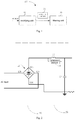
- a surge suppression circuit 100 including a rectifying unit 10, a filtering unit 20 and a protection element 30.
- the surge suppression circuit 100 may be used as a switching unit to supply power to a magnetron of an inverter microwave oven. When the switching unit is turned on, a strong pulse, i.e., an overvoltage exceeding a normal voltage, is generated. Such an overvoltage will cause damage to electronic components in the circuit.
- the rectifying unit 10 includes a rectifying input part and a rectifying output part.
- the rectifying input part is coupled to a voltage input terminal and configured to convert an input electric supply (i.e., an alternating current AC) into a direct current (DC).
- the filtering unit 20 is coupled to the rectifying output part. Usually, the AC may still exist after rectification, and thus the filtering unit 20 is configured to filter the rectified current to obtain a relatively pure DC.
- the protection element 30 is disposed on the rectifying output part and coupled to the filtering unit 20, and configured to suppress an overvoltage of the rectifying output part when a surge occurs.
- the overvoltage of the rectifying output part may be suppressed by the protection element 30 when the surge occurs, thereby improving a circuit reliability of the rectifying unit 10 and the entire microwave oven.
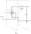
- the rectifying unit 10 includes a bridge rectifier 12.
- Pins 12b and 12c of the bridge rectifier are coupled to the voltage input terminal, that is, to the rectifying input part of the rectifying unit 10, and pins 12a and 12d are coupled to the filtering unit 20, that is, to the rectifying output part of the rectifying unit 10.
- the pins 12a and 12d may be served as two rectifying output terminals.
- the filtering unit 20 includes an inductor 22 and a first capacitor 24.
- a first terminal of the inductor 22 is coupled to one rectifying output terminal 12a, and a second terminal of the inductor 22 is coupled to a first terminal of the first capacitor 24.
- a second terminal of the first capacitor 24 is coupled to the other rectifying output terminal 12d and a ground terminal.
- the protection element 30 is coupled in parallel with the inductor 22.
- the direct current output from the rectifying unit 10 is not a pure direct current and still contains an alternating current part. It is known that an inductive element may be used to pass a direct current and block an alternating current. The alternating current part may be filtered by the inductor 22. However, since the inductance 22 has a limited ability to block the alternating current, a first capacitor 24 is further used for filtering the alternative current after the inductor 22 due to a capacitor nature of passing an alternating current and blocking a direct current. The alternative current may be bypassed to the ground by the first capacitor 24. On this basis, a relative pure direct current may be obtained. In addition, the inductor 22 is also configured to suppress differential mode interference between power lines when the system is powered on.
- the protection element 30 is provided on the rectifying output part of the rectifying unit 10 to effectively suppress the reverse voltage to improve the reliability of the rectifying unit 10.
- the protection element 30 is a second capacitor 32, and the second capacitor 32 is coupled in parallel with the inductor 22. As such, the reverse induced voltage generated by the inductor 22 during the surge may be absorbed by the second capacitor 32, thereby reducing the reverse voltage of the output terminal of the rectifying unit 10.
- the protection element 30 is a first discharge tube 34, and the first discharge tube 34 is coupled in parallel with the inductor 22.
- the discharge tube is configured to protect a target component from a high voltage. When the voltage across the discharge tube is higher than a protection standard, a short circuit will occur inside and an overvoltage input will be absorbed.
- the discharge tube may typically be a gas discharge tube or a semiconductor discharge tube. Similar to the second capacitor 32, the first discharge tube 34 may be configured to suppress the reverse induced voltage generated by the inductor 22 during the surge to reduce the reverse voltage of the output terminal of the rectifying unit 10.
- the protection element 30 is a third capacitor 33, and the third capacitor 33 is coupled in parallel with the two output terminals 12a and 12d of the rectifying unit 10. Similar to the second capacitor 32, the reverse voltage of the rectifying output part of the rectifying unit 10 caused by the surge may be absorbed by the third capacitor 33.
- the protection element 30 is a second discharge tube 35, and the second discharge tube 35 is coupled in parallel with the two output terminals 12a and 12d of the rectifying unit 10. Similar to the first discharge tube 34, the reverse voltage of the rectifying output part of the rectifying unit 10 caused by the surge may be absorbed by the second discharge tube 35.
- the protection element 30 may also be a transient voltage suppressor (TVS). Similar to the capacitor and the discharge tube, the TVS may be configured to absorb a large current in an instant and clamp the terminal voltage to a predetermined value, thus avoiding damages to a protected component due to a transient high-energy impact.
- TVS transient voltage suppressor
- the surge suppression circuit further includes an inverter unit 40 and a voltage doubler rectifying unit 50.
- the inverter unit 40 is coupled to the filtering unit 20 and configured to convert a direct current output from the filtering unit 20 into an alternating current.
- the voltage doubler rectifying unit 50 is coupled to the inverter unit 40 and configured to boost and covert the alternating current output from the inverter unit into a high voltage direct current and supply a power.
- the inverter unit 40 includes a fourth capacitor 42, an insulated gate bipolar transistor (IGBT) 44 and a transformer 46.
- the transformer 46 includes a primary winding and a secondary winding, and two terminals of the primary winding are coupled to two terminals of the fourth capacitor 42 to form a resonant circuit.
- the secondary winding of the transformer 46 is coupled to the voltage doubler rectifying unit 50.
- a first terminal of the fourth capacitor 42 is coupled to a collector of the IGBT 44 and a second terminal of the fourth capacitor 42 is coupled to the filtering unit 20, and an emitter of the IGBT 44 is coupled to the filtering unit 20 via a resistor 60.
- the IGBT 44 is served as a switch to control a resonant circuit.
- the current may be conducted or not conducted according to the required alternating frequency, such that the direct current is divided according to the required frequency, thus converting the direct current into the alternating current.
- the alternating current frequency is usually required to be high, that is, the IGBT 44 is configured to control the resonant circuit to generate a high frequency alternating current.
- the high frequency alternating current is output from the primary level to the secondary level of the transformer.
- the protection element 30 is coupled in parallel with the two rectifying output terminals of the rectifying unit 10.
- the microwave oven according to an embodiment of the present disclosure includes the surge suppression circuit 100 of any of the above embodiments.
- the protection element 30 in the surge suppression circuit 100 provided in the microwave oven can suppress the overvoltage of the rectifying output part caused by the surge, thus improving the circuit reliability of the rectifying unit 10 and the entire microwave oven, and also improving the anti-surge capability and the reliability of the whole machine.
- the microwave oven is an inverter microwave oven.
- the house current with a frequency of 50 Hz may be converted to a high frequency output current by the surge suppression circuit 100 as described above, such that an output power may be controlled by the inverter microwave oven during a heating process and a heating efficiency is improved.
- first and second are used herein for purposes of description and are not intended to indicate or imply a relative importance or an amount of a feature.
- the feature defined with “first” and “second” may include one or more this feature.
- a plurality of' means at least two, for example, two or three.
Landscapes
- Engineering & Computer Science (AREA)
- Power Engineering (AREA)
- Chemical & Material Sciences (AREA)
- Combustion & Propulsion (AREA)
- Mechanical Engineering (AREA)
- General Engineering & Computer Science (AREA)
- Physics & Mathematics (AREA)
- Electromagnetism (AREA)
- Emergency Protection Circuit Devices (AREA)
- Inverter Devices (AREA)
- Rectifiers (AREA)
- Control Of High-Frequency Heating Circuits (AREA)
Abstract
Description
- This application claims a priority to and benefits of Chinese Patent Application Serial No.
201610196929.5 201620262277.6 - The present disclosure relates to a household appliance field, and more particularly to a surge suppression circuit and a microwave oven.
- In the related art of the inverter microwave oven, when a surge voltage exists in a circuit supplying power to a magnetron, the surge voltage may be increased by a reverse voltage generated by an inductor of a filtering unit, and thus a rectifying unit may be broken down by the overvoltage and the circuit may be damaged.
- Embodiments of the present disclosure seek to solve at least one of the problems existing in the related art to at least some extent. Accordingly, embodiments of the present disclosure provide a surge suppression circuit and a microwave oven.
- The surge suppression circuit includes:
- a rectifying unit including
- a rectifying input part coupled to a voltage input terminal, and
- a rectifying output part;
- a filtering unit coupled to the rectifying output part; and
- a protection element disposed on the rectifying output part and coupled to the filtering unit, and configured to suppress an overvoltage of the rectifying output part when a surge occurs.
- In the surge suppression circuit described above, the protection element is able to suppress the overvoltage of the rectifying output part when a surge occurs, thus improving a circuit reliability of the rectifying unit and the entire microwave oven.
- In some embodiments, the rectifying output part includes two rectifying output terminals; the filtering unit includes:
- an inductor, a first terminal of the inductor being coupled to one of the rectifying output terminals, and
- a first capacitor, a first terminal of the first capacitor being coupled to a second terminal of the inductor and a second terminal of the first capacitor being coupled to the other one of the rectifying output terminals and a ground terminal; and
- the protection element is coupled in parallel with the inductor.
- In some embodiments, the protection element is a second capacitor.
- In some embodiments, the protection element is a discharge tube.
- In some embodiments, the rectifying output part includes two rectifying output terminals, and the protection element is coupled in parallel with the two rectifying output terminals.
- In some embodiments, the protection element is a capacitor.
- In some embodiments, the protection element is a discharge tube.
- In some embodiments, the surge suppression circuit further includes:
- an inverter unit coupled to the filtering unit and configured to convert a direct current output from the filtering unit into an alternating current, and
- a voltage doubler rectifying unit coupled to the inverter unit and configured to boost and covert the alternating current output from the inverter unit into a high voltage direct current and supply a power.
- In some embodiments, the inverter unit includes a capacitor, an insulated gate bipolar transistor (IGBT) and a transformer, in which
two terminals of the capacitor are coupled to two primary winding terminals of the transformer to form a resonant circuit, and a secondary winding terminal of the transformer is coupled to the voltage doubler rectifying unit;
a first terminal of the capacitor is coupled to a collector of the IGBT and a second terminal of the capacitor is coupled to the filtering unit, and an emitter of the IGBT is coupled to the filtering unit via a resistor;
the IGBT is configured to control the resonant circuit to generate a high frequency alternating current. - A microwave oven is provided, including a surge suppression circuit according to any of above embodiments.
- The
surge suppression circuit 100 is provided in the microwave oven described above. - The protection element in the surge suppression circuit can suppress the overvoltage of the rectifying output part caused by the surge, thus improving the circuit reliability of the rectifying
unit 10 and the entire microwave oven, and also improving the anti-surge capability and the reliability of the whole machine. - Additional aspects and advantages of embodiments of present disclosure will be given in part in the following descriptions, become apparent in part from the following descriptions, or be learned from the practice of the embodiments of the present disclosure.
-
-
Fig. 1 is a block diagram of a surge suppression circuit according to an embodiment of the present disclosure. -
Fig. 2 is a schematic diagram of a surge suppression circuit according to an embodiment of the present disclosure. -
Fig. 3 is a schematic diagram of a surge suppression circuit according to another embodiment of the present disclosure. -
Fig. 4 is a schematic diagram of a surge suppression circuit according to a further embodiment of the present disclosure. -
Fig. 5 is a schematic diagram of a surge suppression circuit according to a still further embodiment of the present disclosure. -
Fig. 6 is a schematic diagram of a surge suppression circuit according to a still further embodiment of the present disclosure. -
Fig. 7 is a block diagram of a surge suppression circuit according to an embodiment of the present disclosure. -
Fig. 8 is a schematic diagram of a surge suppression circuit according to a still further embodiment of the present disclosure. - Embodiments of the present disclosure are described in detail below, examples of which are illustrated in the drawings. The same or similar elements are denoted by same reference numerals in different drawings unless indicated otherwise. The embodiments described herein with reference to drawings are explanatory, and used to generally understand the present disclosure. The embodiments shall not be construed to limit the present disclosure.
- In the present disclosure, it should be understood that terms such as "first" and "second" are used herein for purposes of description and are not intended to indicate or imply a relative importance or an amount of a feature. Thus, the feature defined with "first" and "second" may include one or more this feature. In the description of the present disclosure, unless specified otherwise, "a plurality of' means two or more than two.
- In the present disclosure, unless specified or limited otherwise, the terms "mounted", "connected", "coupled" and the like are used broadly, and may be, for example, fixed connections, detachable connections, or integral connections; may also be mechanical or electrical connections; may also be direct connections or indirect connections via intervening structures; may also be inner communications of two elements, which can be understood by those skilled in the art according to specific situations.
- Various embodiments and examples are provided in the following description to implement different structures of the present disclosure. In order to simplify the present disclosure, certain elements and settings will be described. However, these elements and settings are only by way of example and are not intended to limit the present disclosure. In addition, reference numerals may be repeated in different examples in the present disclosure. This repeating is for the purpose of simplification and clarity and does not refer to relations between different embodiments and/or settings. Furthermore, examples of different processes and materials are provided in the present disclosure. However, it would be appreciated by those skilled in the art that other processes and/or materials may be also applied.
- With reference to
Fig. 1 , embodiments of the present disclosure provide asurge suppression circuit 100, including a rectifyingunit 10, afiltering unit 20 and aprotection element 30. - The
surge suppression circuit 100 may be used as a switching unit to supply power to a magnetron of an inverter microwave oven. When the switching unit is turned on, a strong pulse, i.e., an overvoltage exceeding a normal voltage, is generated. Such an overvoltage will cause damage to electronic components in the circuit. - The rectifying
unit 10 includes a rectifying input part and a rectifying output part. The rectifying input part is coupled to a voltage input terminal and configured to convert an input electric supply (i.e., an alternating current AC) into a direct current (DC). Thefiltering unit 20 is coupled to the rectifying output part. Usually, the AC may still exist after rectification, and thus thefiltering unit 20 is configured to filter the rectified current to obtain a relatively pure DC. Theprotection element 30 is disposed on the rectifying output part and coupled to thefiltering unit 20, and configured to suppress an overvoltage of the rectifying output part when a surge occurs. - In the
surge suppression circuit 100 described above, the overvoltage of the rectifying output part may be suppressed by theprotection element 30 when the surge occurs, thereby improving a circuit reliability of the rectifyingunit 10 and the entire microwave oven. - Specifically, the rectifying
unit 10 includes abridge rectifier 12.Pins unit 10, and pins 12a and 12d are coupled to thefiltering unit 20, that is, to the rectifying output part of the rectifyingunit 10. Thepins 12a and 12d may be served as two rectifying output terminals. - In some embodiments, with reference to
Fig. 2 , thefiltering unit 20 includes aninductor 22 and afirst capacitor 24. A first terminal of theinductor 22 is coupled to one rectifying output terminal 12a, and a second terminal of theinductor 22 is coupled to a first terminal of thefirst capacitor 24. A second terminal of thefirst capacitor 24 is coupled to the otherrectifying output terminal 12d and a ground terminal. Theprotection element 30 is coupled in parallel with theinductor 22. - The direct current output from the rectifying
unit 10 is not a pure direct current and still contains an alternating current part. It is known that an inductive element may be used to pass a direct current and block an alternating current. The alternating current part may be filtered by theinductor 22. However, since theinductance 22 has a limited ability to block the alternating current, afirst capacitor 24 is further used for filtering the alternative current after theinductor 22 due to a capacitor nature of passing an alternating current and blocking a direct current. The alternative current may be bypassed to the ground by thefirst capacitor 24. On this basis, a relative pure direct current may be obtained. In addition, theinductor 22 is also configured to suppress differential mode interference between power lines when the system is powered on. - Since a reverse induced voltage may be generated by the
inductor 22, an addition of the reverse voltage and the surge voltage may increase the overvoltage, such that the reverse voltage of the rectifying output part of the rectifyingunit 10 may be very high, thus damaging the rectifyingunit 10. Theprotection element 30 is provided on the rectifying output part of the rectifyingunit 10 to effectively suppress the reverse voltage to improve the reliability of the rectifyingunit 10. - With reference to
Fig. 3 , in some embodiments, theprotection element 30 is asecond capacitor 32, and thesecond capacitor 32 is coupled in parallel with theinductor 22. As such, the reverse induced voltage generated by theinductor 22 during the surge may be absorbed by thesecond capacitor 32, thereby reducing the reverse voltage of the output terminal of the rectifyingunit 10. - With reference to
Fig. 4 , in some embodiments, theprotection element 30 is afirst discharge tube 34, and thefirst discharge tube 34 is coupled in parallel with theinductor 22. The discharge tube is configured to protect a target component from a high voltage. When the voltage across the discharge tube is higher than a protection standard, a short circuit will occur inside and an overvoltage input will be absorbed. The discharge tube may typically be a gas discharge tube or a semiconductor discharge tube. Similar to thesecond capacitor 32, thefirst discharge tube 34 may be configured to suppress the reverse induced voltage generated by theinductor 22 during the surge to reduce the reverse voltage of the output terminal of the rectifyingunit 10. - With reference to
Fig. 5 , in some embodiments, theprotection element 30 is a third capacitor 33, and the third capacitor 33 is coupled in parallel with the twooutput terminals 12a and 12d of the rectifyingunit 10. Similar to thesecond capacitor 32, the reverse voltage of the rectifying output part of the rectifyingunit 10 caused by the surge may be absorbed by the third capacitor 33. - With reference to
Fig. 6 , in some embodiments, theprotection element 30 is asecond discharge tube 35, and thesecond discharge tube 35 is coupled in parallel with the twooutput terminals 12a and 12d of the rectifyingunit 10. Similar to thefirst discharge tube 34, the reverse voltage of the rectifying output part of the rectifyingunit 10 caused by the surge may be absorbed by thesecond discharge tube 35. - In addition, the
protection element 30 may also be a transient voltage suppressor (TVS). Similar to the capacitor and the discharge tube, the TVS may be configured to absorb a large current in an instant and clamp the terminal voltage to a predetermined value, thus avoiding damages to a protected component due to a transient high-energy impact. - With reference to
Fig. 7 , in some embodiments, the surge suppression circuit further includes aninverter unit 40 and a voltagedoubler rectifying unit 50. Theinverter unit 40 is coupled to thefiltering unit 20 and configured to convert a direct current output from thefiltering unit 20 into an alternating current. The voltagedoubler rectifying unit 50 is coupled to theinverter unit 40 and configured to boost and covert the alternating current output from the inverter unit into a high voltage direct current and supply a power. - Specifically, in some embodiments, with reference to
Fig. 8 , theinverter unit 40 includes afourth capacitor 42, an insulated gate bipolar transistor (IGBT) 44 and atransformer 46. Thetransformer 46 includes a primary winding and a secondary winding, and two terminals of the primary winding are coupled to two terminals of thefourth capacitor 42 to form a resonant circuit. The secondary winding of thetransformer 46 is coupled to the voltagedoubler rectifying unit 50. - A first terminal of the
fourth capacitor 42 is coupled to a collector of theIGBT 44 and a second terminal of thefourth capacitor 42 is coupled to thefiltering unit 20, and an emitter of theIGBT 44 is coupled to thefiltering unit 20 via a resistor 60. - The
IGBT 44 is served as a switch to control a resonant circuit. When a direct current is input to theIGBT 44, the current may be conducted or not conducted according to the required alternating frequency, such that the direct current is divided according to the required frequency, thus converting the direct current into the alternating current. Moreover, the alternating current frequency is usually required to be high, that is, theIGBT 44 is configured to control the resonant circuit to generate a high frequency alternating current. The high frequency alternating current is output from the primary level to the secondary level of the transformer. - It should be understood that, in the circuit shown in
Fig. 8 , as an example, theprotection element 30 is coupled in parallel with the two rectifying output terminals of the rectifyingunit 10. - The microwave oven according to an embodiment of the present disclosure includes the
surge suppression circuit 100 of any of the above embodiments. - Therefore, the
protection element 30 in thesurge suppression circuit 100 provided in the microwave oven can suppress the overvoltage of the rectifying output part caused by the surge, thus improving the circuit reliability of the rectifyingunit 10 and the entire microwave oven, and also improving the anti-surge capability and the reliability of the whole machine. - Specifically, the microwave oven is an inverter microwave oven. The house current with a frequency of 50 Hz may be converted to a high frequency output current by the
surge suppression circuit 100 as described above, such that an output power may be controlled by the inverter microwave oven during a heating process and a heating efficiency is improved. - Reference throughout this specification to "an embodiment", "some embodiments", "a schematic embodiment", "an example", "a specific example" or "some examples" means that a particular feature, structure, material, or characteristic described in connection with the embodiment or example is included in at least one embodiment or example of the present disclosure. Thus, the appearances of the above phrases in various places throughout this specification are not necessarily referring to the same embodiment or example of the present disclosure. Furthermore, the particular features, structures, materials, or characteristics may be combined in any suitable manner in one or more embodiments or examples.
- In addition, terms such as "first" and "second" are used herein for purposes of description and are not intended to indicate or imply a relative importance or an amount of a feature. Thus, the feature defined with "first" and "second" may include one or more this feature. In the description of the present disclosure, unless specified otherwise, "a plurality of' means at least two, for example, two or three.
- Although explanatory embodiments have been shown and described, it would be appreciated by those skilled in the art that the above embodiments cannot be construed to limit the present disclosure, and changes, alternatives, and modifications can be made in the embodiments without departing from spirit, principles and scope of the present disclosure.
Claims (10)
- A surge suppression circuit, comprising:a rectifying unit comprisinga rectifying input part coupled to a voltage input terminal, anda rectifying output part;a filtering unit coupled to the rectifying output part; anda protection element disposed on the rectifying output part and coupled to the filtering unit, and configured to suppress an overvoltage of the rectifying output part when a surge occurs.
- The surge suppression circuit according to claim 1, wherein
the rectifying output part comprises two rectifying output terminals;
the filtering unit comprises:an inductor, a first terminal of the inductor being coupled to one of the rectifying output terminals, anda first capacitor, a first terminal of the first capacitor being coupled to a second terminal of the inductor and a second terminal of the first capacitor being coupled to the other one of the rectifying output terminals and a ground terminal;and
the protection element is coupled in parallel with the inductor. - The surge suppression circuit according to claim 2, wherein the protection element is a second capacitor.
- The surge suppression circuit according to claim 2, wherein the protection element is a discharge tube.
- The surge suppression circuit according to claim 1, wherein the rectifying output part comprises two rectifying output terminals, and the protection element is coupled in parallel with the two rectifying output terminals.
- The surge suppression circuit according to claim 5, wherein the protection element is a capacitor.
- The surge suppression circuit according to claim 5, wherein the protection element is a discharge tube.
- The surge suppression circuit according to claim 1, further comprising:an inverter unit coupled to the filtering unit and configured to convert a direct current output from the filtering unit into an alternating current, anda voltage doubler rectifying unit coupled to the inverter unit and configured to boost and covert the alternating current output from the inverter unit into a high voltage direct current and supply a power.
- The surge suppression circuit according to claim 8, wherein the inverter unit comprises a capacitor, an insulated gate bipolar transistor (IGBT) and a transformer, wherein
two terminals of the capacitor are coupled to two primary winding terminals of the transformer to form a resonant circuit, and a secondary winding terminal of the transformer is coupled to the voltage doubler rectifying unit;
a first terminal of the capacitor is coupled to a collector of the IGBT and a second terminal of the capacitor is coupled to the filtering unit, and an emitter of the IGBT is coupled to the filtering unit via a resistor;
the IGBT is configured to control the resonant circuit to generate a high frequency alternating current. - A microwave oven, comprising a surge suppression circuit according to any one of claims 1-9.
Applications Claiming Priority (3)
| Application Number | Priority Date | Filing Date | Title |
|---|---|---|---|
| CN201610196929.5A CN105605628B (en) | 2016-03-30 | 2016-03-30 | Surge restraint circuit and micro-wave oven |
| CN201620262277.6U CN205641039U (en) | 2016-03-30 | 2016-03-30 | Surge suppression circuit and microwave oven |
| PCT/CN2016/086389 WO2017166445A1 (en) | 2016-03-30 | 2016-06-20 | Surge suppression circuit and microwave oven |
Publications (3)
| Publication Number | Publication Date |
|---|---|
| EP3438543A1 true EP3438543A1 (en) | 2019-02-06 |
| EP3438543A4 EP3438543A4 (en) | 2019-04-24 |
| EP3438543B1 EP3438543B1 (en) | 2025-10-01 |
Family
ID=59963349
Family Applications (1)
| Application Number | Title | Priority Date | Filing Date |
|---|---|---|---|
| EP16896218.1A Active EP3438543B1 (en) | 2016-03-30 | 2016-06-20 | Surge suppression circuit and microwave oven |
Country Status (4)
| Country | Link |
|---|---|
| US (1) | US20190131786A1 (en) |
| EP (1) | EP3438543B1 (en) |
| ES (1) | ES3056558T3 (en) |
| WO (1) | WO2017166445A1 (en) |
Family Cites Families (16)
| Publication number | Priority date | Publication date | Assignee | Title |
|---|---|---|---|---|
| US3118102A (en) * | 1960-12-14 | 1964-01-14 | Ledex Inc | Diode rectifier with overvoltage protection |
| IT1111543B (en) * | 1978-03-17 | 1986-01-13 | Rca Corp | CIRCUIT FOR THE PROTECTION OF A POWER RECTIFIER FROM VOLTAGE LOSSES |
| JPS58201575A (en) * | 1982-05-19 | 1983-11-24 | Hitachi Ltd | Switching regulator overcurrent detection circuit |
| US4691263A (en) * | 1985-12-17 | 1987-09-01 | Westinghouse Electric Corp. | Low leakage, solid state a-c power contact |
| JP3116565B2 (en) * | 1991-09-17 | 2000-12-11 | ソニー株式会社 | Line filter transformer and power supply circuit |
| JP3358645B2 (en) * | 1995-10-05 | 2002-12-24 | 株式会社リコー | Switching regulator |
| CN1125578C (en) * | 1998-08-06 | 2003-10-22 | 松下电器产业株式会社 | High frequency heating apparatus |
| JP2010041790A (en) * | 2008-08-04 | 2010-02-18 | Fuji Electric Systems Co Ltd | Power conversion apparatus |
| CN201774706U (en) * | 2010-02-04 | 2011-03-23 | 安徽科发信息科技有限公司 | Semiconductor LED lighting high brightness zenith lighting drive circuit |
| CN101854766B (en) * | 2010-04-23 | 2013-03-27 | 清华大学 | Electrodeless lamp power circuit, and protection method and protective circuit thereof |
| JP5811329B2 (en) * | 2011-07-08 | 2015-11-11 | 東芝ライテック株式会社 | Power supply |
| KR101142415B1 (en) * | 2011-09-30 | 2012-05-07 | 주식회사 디에스이 | Power control apparatus for light bulb with fine tuning high power factor able to adjust brightness |
| KR101312635B1 (en) * | 2012-02-10 | 2013-10-04 | 주식회사 디에스이 | Low Voltage Driving Prevention Apparatus for Light Emitting Diode Lamp |
| CN203746771U (en) * | 2014-03-04 | 2014-07-30 | 乐星产电(无锡)有限公司 | Over-voltage tripping device |
| CN204906192U (en) * | 2015-09-14 | 2015-12-23 | 航天长峰朝阳电源有限公司 | Boost module is recommended to wide region full cut -off ring high efficiency |
| CN105605628B (en) * | 2016-03-30 | 2018-06-19 | 广东美的厨房电器制造有限公司 | Surge restraint circuit and micro-wave oven |
-
2016
- 2016-06-20 WO PCT/CN2016/086389 patent/WO2017166445A1/en not_active Ceased
- 2016-06-20 ES ES16896218T patent/ES3056558T3/en active Active
- 2016-06-20 EP EP16896218.1A patent/EP3438543B1/en active Active
-
2018
- 2018-10-27 US US16/172,730 patent/US20190131786A1/en not_active Abandoned
Also Published As
| Publication number | Publication date |
|---|---|
| EP3438543A4 (en) | 2019-04-24 |
| ES3056558T3 (en) | 2026-02-23 |
| WO2017166445A1 (en) | 2017-10-05 |
| US20190131786A1 (en) | 2019-05-02 |
| EP3438543B1 (en) | 2025-10-01 |
Similar Documents
| Publication | Publication Date | Title |
|---|---|---|
| US9231481B2 (en) | Power converter apparatus | |
| US8976550B2 (en) | Power supply having a surge protection circuit | |
| Lai et al. | Development of a 10 kW high power density three-phase ac-dc-ac converter using SiC devices | |
| EP3432457A1 (en) | Method and apparatus for reducing noise generated by rectification diode located at primary side of switching power supply | |
| US20170063216A1 (en) | Power conversion device | |
| US20110044080A1 (en) | Converter | |
| EP2672597A1 (en) | Voltage rectifier | |
| US9742261B2 (en) | Power factor correction circuit | |
| CN109905017A (en) | Auxiliary converter circuit, AuCT and auxiliary converter cabinet | |
| EP3438543B1 (en) | Surge suppression circuit and microwave oven | |
| US8823336B2 (en) | Bridgeless power factor corrector with single choke and method of operating the same | |
| CN105605628B (en) | Surge restraint circuit and micro-wave oven | |
| CN208112521U (en) | A kind of lightning protection power source | |
| Chakraborty et al. | Design concept of a high power high frequency power supply for feeding 500 kV, 100 mA Cockcroft-Walton generator | |
| US20160198538A1 (en) | Led drive circuit | |
| Jeong et al. | Design of 35 kJ/s 25 kV capacitor charging power supply for pulsed power systems | |
| US11575309B2 (en) | Method and device for damping of LCL filter during start-up of an electronic appliance | |
| CN205641039U (en) | Surge suppression circuit and microwave oven | |
| JP3231935B2 (en) | Inverter power supply | |
| CN205754103U (en) | A kind of motor magnetic circuit controls efficient energy-saving device | |
| JPH09285000A (en) | Switching regulator | |
| CN106922044B (en) | Microwave oven power supply circuit and microwave oven | |
| US12288981B2 (en) | Surge protection circuit | |
| CN110401336A (en) | AC input circuit and air conditioner | |
| JP2018117256A (en) | Clamp type semiconductor device and switching power supply device |
Legal Events
| Date | Code | Title | Description |
|---|---|---|---|
| STAA | Information on the status of an ep patent application or granted ep patent |
Free format text: STATUS: THE INTERNATIONAL PUBLICATION HAS BEEN MADE |
|
| PUAI | Public reference made under article 153(3) epc to a published international application that has entered the european phase |
Free format text: ORIGINAL CODE: 0009012 |
|
| STAA | Information on the status of an ep patent application or granted ep patent |
Free format text: STATUS: REQUEST FOR EXAMINATION WAS MADE |
|
| 17P | Request for examination filed |
Effective date: 20181026 |
|
| AK | Designated contracting states |
Kind code of ref document: A1 Designated state(s): AL AT BE BG CH CY CZ DE DK EE ES FI FR GB GR HR HU IE IS IT LI LT LU LV MC MK MT NL NO PL PT RO RS SE SI SK SM TR |
|
| AX | Request for extension of the european patent |
Extension state: BA ME |
|
| A4 | Supplementary search report drawn up and despatched |
Effective date: 20190326 |
|
| RIC1 | Information provided on ipc code assigned before grant |
Ipc: H02M 7/06 20060101ALI20190320BHEP Ipc: F24C 7/08 20060101ALI20190320BHEP Ipc: F24C 7/02 20060101AFI20190320BHEP Ipc: H05B 6/66 20060101ALI20190320BHEP |
|
| DAV | Request for validation of the european patent (deleted) | ||
| DAX | Request for extension of the european patent (deleted) | ||
| STAA | Information on the status of an ep patent application or granted ep patent |
Free format text: STATUS: EXAMINATION IS IN PROGRESS |
|
| 17Q | First examination report despatched |
Effective date: 20191122 |
|
| GRAP | Despatch of communication of intention to grant a patent |
Free format text: ORIGINAL CODE: EPIDOSNIGR1 |
|
| STAA | Information on the status of an ep patent application or granted ep patent |
Free format text: STATUS: GRANT OF PATENT IS INTENDED |
|
| INTG | Intention to grant announced |
Effective date: 20250520 |
|
| GRAS | Grant fee paid |
Free format text: ORIGINAL CODE: EPIDOSNIGR3 |
|
| GRAA | (expected) grant |
Free format text: ORIGINAL CODE: 0009210 |
|
| STAA | Information on the status of an ep patent application or granted ep patent |
Free format text: STATUS: THE PATENT HAS BEEN GRANTED |
|
| AK | Designated contracting states |
Kind code of ref document: B1 Designated state(s): AL AT BE BG CH CY CZ DE DK EE ES FI FR GB GR HR HU IE IS IT LI LT LU LV MC MK MT NL NO PL PT RO RS SE SI SK SM TR |
|
| REG | Reference to a national code |
Ref country code: GB Ref legal event code: FG4D Ref country code: CH Ref legal event code: F10 Free format text: ST27 STATUS EVENT CODE: U-0-0-F10-F00 (AS PROVIDED BY THE NATIONAL OFFICE) Effective date: 20251001 |
|
| REG | Reference to a national code |
Ref country code: IE Ref legal event code: FG4D |
|
| REG | Reference to a national code |
Ref country code: DE Ref legal event code: R096 Ref document number: 602016093736 Country of ref document: DE |
|
| REG | Reference to a national code |
Ref country code: NL Ref legal event code: FP |
|
| REG | Reference to a national code |
Ref country code: ES Ref legal event code: FG2A Ref document number: 3056558 Country of ref document: ES Kind code of ref document: T3 Effective date: 20260223 |
|
| REG | Reference to a national code |
Ref country code: AT Ref legal event code: MK05 Ref document number: 1842817 Country of ref document: AT Kind code of ref document: T Effective date: 20251001 |
|
| REG | Reference to a national code |
Ref country code: LT Ref legal event code: MG9D |
|
| PG25 | Lapsed in a contracting state [announced via postgrant information from national office to epo] |
Ref country code: NO Free format text: LAPSE BECAUSE OF FAILURE TO SUBMIT A TRANSLATION OF THE DESCRIPTION OR TO PAY THE FEE WITHIN THE PRESCRIBED TIME-LIMIT Effective date: 20260101 |
|
| PG25 | Lapsed in a contracting state [announced via postgrant information from national office to epo] |
Ref country code: FI Free format text: LAPSE BECAUSE OF FAILURE TO SUBMIT A TRANSLATION OF THE DESCRIPTION OR TO PAY THE FEE WITHIN THE PRESCRIBED TIME-LIMIT Effective date: 20251001 Ref country code: AT Free format text: LAPSE BECAUSE OF FAILURE TO SUBMIT A TRANSLATION OF THE DESCRIPTION OR TO PAY THE FEE WITHIN THE PRESCRIBED TIME-LIMIT Effective date: 20251001 Ref country code: HR Free format text: LAPSE BECAUSE OF FAILURE TO SUBMIT A TRANSLATION OF THE DESCRIPTION OR TO PAY THE FEE WITHIN THE PRESCRIBED TIME-LIMIT Effective date: 20251001 |
|
| PG25 | Lapsed in a contracting state [announced via postgrant information from national office to epo] |
Ref country code: RS Free format text: LAPSE BECAUSE OF FAILURE TO SUBMIT A TRANSLATION OF THE DESCRIPTION OR TO PAY THE FEE WITHIN THE PRESCRIBED TIME-LIMIT Effective date: 20260101 |
|
| PG25 | Lapsed in a contracting state [announced via postgrant information from national office to epo] |
Ref country code: IS Free format text: LAPSE BECAUSE OF FAILURE TO SUBMIT A TRANSLATION OF THE DESCRIPTION OR TO PAY THE FEE WITHIN THE PRESCRIBED TIME-LIMIT Effective date: 20260201 |
|
| PG25 | Lapsed in a contracting state [announced via postgrant information from national office to epo] |
Ref country code: PT Free format text: LAPSE BECAUSE OF FAILURE TO SUBMIT A TRANSLATION OF THE DESCRIPTION OR TO PAY THE FEE WITHIN THE PRESCRIBED TIME-LIMIT Effective date: 20260202 Ref country code: CZ Free format text: LAPSE BECAUSE OF FAILURE TO SUBMIT A TRANSLATION OF THE DESCRIPTION OR TO PAY THE FEE WITHIN THE PRESCRIBED TIME-LIMIT Effective date: 20251001 |
|
| PG25 | Lapsed in a contracting state [announced via postgrant information from national office to epo] |
Ref country code: PL Free format text: LAPSE BECAUSE OF FAILURE TO SUBMIT A TRANSLATION OF THE DESCRIPTION OR TO PAY THE FEE WITHIN THE PRESCRIBED TIME-LIMIT Effective date: 20251001 |
|
| PG25 | Lapsed in a contracting state [announced via postgrant information from national office to epo] |
Ref country code: LV Free format text: LAPSE BECAUSE OF FAILURE TO SUBMIT A TRANSLATION OF THE DESCRIPTION OR TO PAY THE FEE WITHIN THE PRESCRIBED TIME-LIMIT Effective date: 20251001 |
|
| PG25 | Lapsed in a contracting state [announced via postgrant information from national office to epo] |
Ref country code: BG Free format text: LAPSE BECAUSE OF FAILURE TO SUBMIT A TRANSLATION OF THE DESCRIPTION OR TO PAY THE FEE WITHIN THE PRESCRIBED TIME-LIMIT Effective date: 20251001 |