EP3437694A1 - Connection pin and feedthrough and production process for a connection pin - Google Patents
Connection pin and feedthrough and production process for a connection pin Download PDFInfo
- Publication number
- EP3437694A1 EP3437694A1 EP18186087.5A EP18186087A EP3437694A1 EP 3437694 A1 EP3437694 A1 EP 3437694A1 EP 18186087 A EP18186087 A EP 18186087A EP 3437694 A1 EP3437694 A1 EP 3437694A1
- Authority
- EP
- European Patent Office
- Prior art keywords
- end section
- flattened end
- connection pin
- pin
- connection
- Prior art date
- Legal status (The legal status is an assumption and is not a legal conclusion. Google has not performed a legal analysis and makes no representation as to the accuracy of the status listed.)
- Withdrawn
Links
- 238000004519 manufacturing process Methods 0.000 title claims description 12
- 239000000463 material Substances 0.000 claims abstract description 28
- 239000004020 conductor Substances 0.000 claims abstract description 25
- 238000000034 method Methods 0.000 claims description 21
- 238000013532 laser treatment Methods 0.000 claims description 12
- 241000587161 Gomphocarpus Species 0.000 claims description 6
- 230000000747 cardiac effect Effects 0.000 claims description 4
- 230000015572 biosynthetic process Effects 0.000 claims description 3
- 230000001788 irregular Effects 0.000 claims description 3
- 229910000679 solder Inorganic materials 0.000 description 5
- 238000013461 design Methods 0.000 description 4
- 238000002679 ablation Methods 0.000 description 3
- RTAQQCXQSZGOHL-UHFFFAOYSA-N Titanium Chemical compound [Ti] RTAQQCXQSZGOHL-UHFFFAOYSA-N 0.000 description 2
- 229910052802 copper Inorganic materials 0.000 description 2
- 239000010949 copper Substances 0.000 description 2
- 238000011161 development Methods 0.000 description 2
- 230000018109 developmental process Effects 0.000 description 2
- 230000006870 function Effects 0.000 description 2
- 238000009413 insulation Methods 0.000 description 2
- 239000010955 niobium Substances 0.000 description 2
- BASFCYQUMIYNBI-UHFFFAOYSA-N platinum Chemical compound [Pt] BASFCYQUMIYNBI-UHFFFAOYSA-N 0.000 description 2
- 238000012545 processing Methods 0.000 description 2
- 229910052719 titanium Inorganic materials 0.000 description 2
- 239000010936 titanium Substances 0.000 description 2
- RYGMFSIKBFXOCR-UHFFFAOYSA-N Copper Chemical compound [Cu] RYGMFSIKBFXOCR-UHFFFAOYSA-N 0.000 description 1
- ZOKXTWBITQBERF-UHFFFAOYSA-N Molybdenum Chemical compound [Mo] ZOKXTWBITQBERF-UHFFFAOYSA-N 0.000 description 1
- 238000005452 bending Methods 0.000 description 1
- 239000000560 biocompatible material Substances 0.000 description 1
- 239000011248 coating agent Substances 0.000 description 1
- 238000000576 coating method Methods 0.000 description 1
- 238000010276 construction Methods 0.000 description 1
- 230000007547 defect Effects 0.000 description 1
- 230000001419 dependent effect Effects 0.000 description 1
- PCHJSUWPFVWCPO-UHFFFAOYSA-N gold Chemical compound [Au] PCHJSUWPFVWCPO-UHFFFAOYSA-N 0.000 description 1
- 229910052737 gold Inorganic materials 0.000 description 1
- 239000010931 gold Substances 0.000 description 1
- 238000001727 in vivo Methods 0.000 description 1
- 238000009434 installation Methods 0.000 description 1
- 238000005304 joining Methods 0.000 description 1
- 230000007774 longterm Effects 0.000 description 1
- 238000012986 modification Methods 0.000 description 1
- 230000004048 modification Effects 0.000 description 1
- 229910052750 molybdenum Inorganic materials 0.000 description 1
- 239000011733 molybdenum Substances 0.000 description 1
- 229910052759 nickel Inorganic materials 0.000 description 1
- 229910052758 niobium Inorganic materials 0.000 description 1
- GUCVJGMIXFAOAE-UHFFFAOYSA-N niobium atom Chemical compound [Nb] GUCVJGMIXFAOAE-UHFFFAOYSA-N 0.000 description 1
- 230000003647 oxidation Effects 0.000 description 1
- 238000007254 oxidation reaction Methods 0.000 description 1
- 229910052697 platinum Inorganic materials 0.000 description 1
- 238000003672 processing method Methods 0.000 description 1
- 229910001285 shape-memory alloy Inorganic materials 0.000 description 1
- 238000005476 soldering Methods 0.000 description 1
- 230000003746 surface roughness Effects 0.000 description 1
- 229910052715 tantalum Inorganic materials 0.000 description 1
- GUVRBAGPIYLISA-UHFFFAOYSA-N tantalum atom Chemical compound [Ta] GUVRBAGPIYLISA-UHFFFAOYSA-N 0.000 description 1
- 238000002560 therapeutic procedure Methods 0.000 description 1
- 238000011282 treatment Methods 0.000 description 1
- 238000003466 welding Methods 0.000 description 1
Images

Classifications
-
- A—HUMAN NECESSITIES
- A61—MEDICAL OR VETERINARY SCIENCE; HYGIENE
- A61N—ELECTROTHERAPY; MAGNETOTHERAPY; RADIATION THERAPY; ULTRASOUND THERAPY
- A61N1/00—Electrotherapy; Circuits therefor
- A61N1/18—Applying electric currents by contact electrodes
- A61N1/32—Applying electric currents by contact electrodes alternating or intermittent currents
- A61N1/36—Applying electric currents by contact electrodes alternating or intermittent currents for stimulation
- A61N1/372—Arrangements in connection with the implantation of stimulators
- A61N1/375—Constructional arrangements, e.g. casings
- A61N1/3752—Details of casing-lead connections
- A61N1/3754—Feedthroughs
-
- A—HUMAN NECESSITIES
- A61—MEDICAL OR VETERINARY SCIENCE; HYGIENE
- A61N—ELECTROTHERAPY; MAGNETOTHERAPY; RADIATION THERAPY; ULTRASOUND THERAPY
- A61N1/00—Electrotherapy; Circuits therefor
- A61N1/18—Applying electric currents by contact electrodes
- A61N1/32—Applying electric currents by contact electrodes alternating or intermittent currents
- A61N1/36—Applying electric currents by contact electrodes alternating or intermittent currents for stimulation
- A61N1/362—Heart stimulators
-
- A—HUMAN NECESSITIES
- A61—MEDICAL OR VETERINARY SCIENCE; HYGIENE
- A61N—ELECTROTHERAPY; MAGNETOTHERAPY; RADIATION THERAPY; ULTRASOUND THERAPY
- A61N1/00—Electrotherapy; Circuits therefor
- A61N1/18—Applying electric currents by contact electrodes
- A61N1/32—Applying electric currents by contact electrodes alternating or intermittent currents
- A61N1/38—Applying electric currents by contact electrodes alternating or intermittent currents for producing shock effects
- A61N1/39—Heart defibrillators
- A61N1/3956—Implantable devices for applying electric shocks to the heart, e.g. for cardioversion
Definitions
- the invention relates to a connection pin of a feedthrough of an implantable medical electronic device, a feedthrough comprising such a connection pin, and a method for producing such a connection pin.
- IMDs implantable electromedical devices
- IMDs implantable electromedical devices
- many devices can selectively measure electrical pulses and stimuli in the body of the patient and record or assess them over a longer period of time to select an individually adapted therapy and to check the success of the treatment in vivo.
- the device has, inside the housing, electronic / electrical functional units for producing and measuring the pulses and for suitable control of the production of pulses, and the device has, on the outside, electrodes directly on it or connections for at least one electrode lead, the distal end section of these connections containing the electrodes for transferring pulses to the tissue.
- the electronic / electrical functional units inside the device are to be connected with the electrodes or electrode lead connections outside in a way that ensures absolutely and permanently reliable function under the special conditions of the implanted state.
- feedthroughs which have been the subject of numerous and quite different developments.
- the task of a feedthrough is to carry the electrical signals through the hermetically sealed housing and in this way to allow the electronics in the hermetically sealed housing to make electrical contact with the electrodes in the body of the patient.
- this is done using connection pins that make contact with the printed circuit board or with a similar conductor support located inside the device, and carry the signals through the housing.
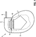
- US 7,747,321 B2 discloses a cardiac pacemaker 1 as shown in Fig. 1 , with a pacemaker housing 3 and a header 5, which has a printed circuit board (PCB) 7 arranged inside it, along with other electronic components, and whose lead connector (not shown) arranged in the header is connected with an electrode lead 9.
- a feedthrough 11 provided between device housing 3 and header 5 comprises multiple connection pins 13. At one end, the connection pins are inserted through a corresponding hole in the printed circuit board and are soft-soldered with it.
- They comprise a wire core, made, for instance, of tantalum, niobium, titanium, molybdenum, or copper, and an oxidation-resistant sheath made of a biocompatible material, for instance gold, platinum, titanium, or something similar.
- EP 3 181 194 A1 discloses a feedthrough comprising connection pins formed out of a shape memory alloy.
- EP 2 965 783 A1 discloses a method for producing a connection pin for a feedthrough from a semi-finished part comprising at least a second layer element comprising a solder.
- connection elements are provided by pin band constructions in which a long connection element (pin) penetrates an insulation body of the feedthrough and is used for welding on to a header of the IMD, while a band welded on to the housing-side end of the pin makes the contact with the device electronics (printed circuit board).
- the pin can consist of materials such as Nb or PtIr and the band can consist of materials such as of Cu or Ni, the pin is hard-soldered in the insulation body, and the band is typically also hard-soldered onto the end of the pin or connected with it through a laser spot weld.
- connection pins that have a so-called nail head, which is made by cold forming a drawn wire material.
- nail head which is made by cold forming a drawn wire material.
- the structure of such connection pins is disadvantageously changed as a consequence of cold forming, and the pins frequently show microcracks in their surface. This produces problems with coating, which is necessary for connecting conductors by a soldering process.
- the surface quality of such connection pins can be affected by drawing grooves, which can, in particular, lead to undesired flowing of connecting solder along the connection pin.
- connection pin whose properties are better with regard to connecting a conductor, especially a band-shaped conductor, by means of a connection process involving material bonding. Furthermore, a suitable production process for such a connection pin should be indicated.
- connection pin for a feedthrough of an implantable medical electronic device, the connection pin comprising: an elongated pin body extending along a longitudinal axis of the pin body; at least one flattened end section that is integrally connected to said pin body, wherein the at least one flattened end section comprises a cross-section area that is smaller than a cross-section area of the pin body; and at least one planar connecting surface formed on the at least one flattened end section.
- said cross-section area of the at least one flattened end section extends perpendicular to one of: an extension direction of the at least one flattened end section, the at least one planar connecting surface, the longitudinal axis of the pin body.
- the cross-section area of the pin body extends perpendicular to the longitudinal axis of the pin body.
- the present invention includes the idea of overcoming certain fundamental disadvantages of connecting the known connection pin by changing the surface geometry, at least in an end section of the pin.
- the invention further includes the idea of producing in the relevant end section - and only there - a surface geometry that can be optimally fitted to band-shaped connection conductors.
- the invention includes the idea of producing, on the pin body, at least one flattened end section on which at least one planar connecting surface is formed, in particular for connection by material bonding of a band-shaped conductor.
- the pin body is cylindrical.
- the at least one planar connecting surface is configured to be bonded to a band-shaped conductor by way of material bonding.
- the at least one planar connecting surface is larger than said cross-section area of the pin body.
- connection pin comprises a further flattened end section opposite the at least one flattened end section, wherein these two end sections are integrally connected to one another by the pin body.
- both end sections of the connection pin are formed as a flattened end section, respectively, wherein on each flattened end section at least one planar connecting surface is formed.
- the connection pin comprises a further end section that is formed as a nail head.
- the further end section / nail head is integrally connected to the at least one flattened end section by the pin body.
- the further flattened end section comprises a cross-section area that is smaller than a cross-section area of the pin body.
- said cross-section area of the further flattened end section extends perpendicular to one of: an extension direction of the further flattened end section, the at least one planar connecting surface of the further flattened end section, the longitudinal axis of the pin body.
- the at least one planar connecting surface of the further flattened end section is larger than said cross-section area of the pin body.
- the at least one flattened end section has two planar connecting surfaces and/or that further flattened end section has two planar connecting surfaces.
- the two planar connecting surfaces of the at least one flattened end section or of the further flattened end section form surfaces that face away from each other.
- the at least one flattened end section and/or the further flattened end section is bent at an angle in the range between 30° and 90°, especially at an angle of 90°, with respect to the longitudinal axis of the (e.g. cylindrical) pin body.
- This bending offers additional degrees of freedom with respect to the shape of the end section of a conductor band to be connected, in particular the shape of the end section of the conductor band that is near the pin, and possibly allows a more compact design of the feedthrough.
- the or every connecting surface (e.g. the at least one planar connecting surface of the at least one flattened end section, or the at least one planar connecting surface of the further flattened end section, or each of said two connecting surfaces of the at least one flattened end section or of the further flattened end section) has a surface structure, especially one oriented essentially transverse to the longitudinal axis or one that is irregular, that prevents a connecting material, which is intended for connection of a band-shaped conductor by material bonding, from running in the direction of the longitudinal axis or towards the pin body.
- the method aspects of the invention include the idea of producing the connection pin starting from a stress relieved, especially annealed wire material, allowing laser processing methods to be used to produce the inventive end section configuration.
- the process aspects of the invention also include the idea of producing this end section configuration using an ultrashort pulse laser treatment.
- a method for producing a connection pin according to the present invention comprising the steps of: providing an annealed wire material, and applying an ultrashort pulse laser treatment to the wire material to form the pin body, the at least one flattened end section, and the at least one planar connecting surface.
- the further flattened end section and the at least one planar connecting surface of the further flattened end section can be formed by applying the ultrashort pulse laser treatment to the wire material.
- said two planar connecting surfaces of the at least one flattened end section or of the further flattened end section can be formed by applying the ultrashort pulse laser treatment.
- One embodiment of the process involves forming, particularly in connection with the formation of the respective flattened end section, a surface structure optimized for connection on the at least one planar connecting surface of the at least one flattened end section (or on every connecting surface), preferably doing so by ultrashort pulse laser treatment. This can be done by a surface structure that is deliberately adapted to the joining partner or by a deliberately directed surface roughness.
- connection pin with high production yield, and also to a durable contact with long-term stability.
- such a surface structure can also be formed by ultrashort pulse laser treatment on the at least one planar connecting surface of the further flattened end section.
- such a surface structure can also be formed by ultrashort pulse laser treatment on the two opposite planar connecting surfaces of the at least one and/or of the further flattened end section (see also above).
- connection pin is installed into a feedthrough of an implantable medical electronic device after the at least one flattened end section and/or after the further flattened end section is formed, and the device-internal end section is bent by cold forming in the installed state.
- This sequence of steps simplifies the realization of feedthroughs with bent connection pins, and under certain circumstances it is the condition that first allows such feedthroughs to be produced.
- An embodiment of this provides that the device-external end section of the connection pin is bent by cold forming before it is installed into the feedthrough.
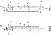
- Fig. 2 is a perspective representation showing a connection pin 20 with a cylindrical pin body 21 extending along a longitudinal axis A, which pin body forms the predominant part of the longitudinal extension of the connection pin, and an e.g. prism-shaped end section 23, which has two opposite planar connecting surfaces 23a, 23b (i.e. the surfaces 23a, 23b face away from each other) onto which surfaces a conductor band (not shown) can be welded.
- the geometric configuration of the end section 23 can be imparted by ultrashort pulse laser treatment or possibly also by a mechanical forming step.
- the flattened end section 23 comprises a cross-section area A' that is smaller than a cross-section area A" of the pin body 21.
- the two cross-section areas A', A" extend perpendicular to the longitudinal axis A of the pin body 21. Furthermore, particularly, the connecting surfaces 23a, 23b can each be larger than the cross-section area A" of the pin body 21. Furthermore, the two surfaces 23a, 23b extend parallel to the longitudinal axis A.
- Fig. 3 shows another embodiment of a connection pin 30, which once again has a cylindrical pin body 31 that extends along a longitudinal axis A over most of the longitudinal extension of the connection pin, but whose opposite ends have two deformed flattened end sections 33, 35 formed by e.g. ablation processing (for example once again by means of an ultrashort pulse laser process).
- ablation processing for example once again by means of an ultrashort pulse laser process.
- the basic cylindrical shape is maintained over most of the cross section, however ablation processing has been used to remove a section of the cylinder, forming, in each case, a planar connecting surface 33a or 35a, to which a conductor band can be welded.
- the two surfaces 33a, 35a can face in opposite directions.
- each end section 23, 33 comprises a cross-section area A' that is smaller than a cross-section area A" of the pin body 31.
- the two cross-section areas A', A" extend perpendicular to the longitudinal axis A of the pin body 31.
- the connecting surfaces 33a, 35a can each be larger than the cross-section area A" of the pin body 21.
- the two planar connecting surfaces 33a, 35a extend parallel to the longitudinal axis A.
- Fig. 4 shows another embodiment of the invention in which a connection pin 40 once again comprises an essentially cylindrical pin body 41, together with a conductor band C.
- both end sections 43, 45 are also processed e.g. with an ablation process to create a planar connecting surface 43a or 45a.
- the connecting surfaces 43a, 45a are structured by microchannels or grooves running transverse to the longitudinal extension / longitudinal axis A of the pin body 41 so as to prevent the running of connecting solder in the longitudinal direction of the connection pin or towards the pin body 41.
- the end section 45 is bent at right angles to the longitudinal axis A of the pin body 41 of the connection pin.
- each end section 43, 45 can comprises a cross-section area A' (perpendicular to the respective connecting surface 43a, 45a) that is smaller than a cross-section area A" of the pin body 41 (perpendicular to longitudinal axis A).
- the connecting surfaces 43a, 45a can each be larger than the cross-section area A" of the pin body 41.
- Fig. 5 shows another embodiment of a connection pin 50 in a configuration which it assumes after installation in a feedthrough (not shown), namely the configuration in which both end sections 53, 55 integrally connected to the pin body 51 are bent at right angles to the longitudinal axis A of the pin body 51.
- the connecting surfaces 53a, 55a can exhibit microroughness, which prevents flowing of solder material in the longitudinal direction of the connection pin, similar to the embodiment in Fig. 4 .
- each end section 53, 55 can comprises a cross-section area A' that is smaller than a cross-section area A" of the pin body 51.
- the connecting surfaces 53a, 55a can each be larger than the cross-section area A" of the pin body 51.
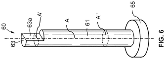
- Fig. 6 shows a modification of the embodiments shown in Figs. 2 to 5 , wherein here one end section of the connection pin 60 forms a nail head 65 that is integrally connected to the pin body 61 that extends along the longitudinal axis A.
- the flattened end section 63 of the connection pin 60 is formed as shown in Fig. 3 , but may also be formed according to one of the other embodiments shown e.g. in Figs. 2 , 4, or 5 .
- the connecting surface 63a can comprise a surface structure comprising e.g.
- the flattened end section 63 can comprises a cross-section area A' (perpendicular to longitudinal axis A) that is smaller than a cross-section area A" (perpendicular to longitudinal axis A) of the pin body 61.
- the connecting surface 63a can be larger than the cross-section area A" of the pin body 21 and can extend parallel to the longitudinal axis A of the pin body 61.
- Item 1 A connection pin (20, 30, 40, 50) of a feedthrough (11) of an implantable medical electronic device (1) with an essentially cylindrical pin body (21; 31; 41; 51) and at least one flattened end section (23; 33, 35; 43, 45; 53, 55) that has at least one planar connecting surface (23a, 23b; 33a, 35a; 43a, 45a; 53a, 55a) formed on it, especially for connection by material bonding of a band-shaped conductor (C).
- a connection pin (20, 30, 40, 50) of a feedthrough (11) of an implantable medical electronic device (1) with an essentially cylindrical pin body (21; 31; 41; 51) and at least one flattened end section (23; 33, 35; 43, 45; 53, 55) that has at least one planar connecting surface (23a, 23b; 33a, 35a; 43a, 45a; 53a, 55a) formed on it, especially for connection by material bonding of a band-shaped conductor (C).
- Item 2 A connection pin according to item 1, wherein both ends of the pin body (31; 41; 51) have a flattened end section (33, 35; 43, 45; 53, 55), on which at least one planar connecting surface (33a, 35a; 43a, 45a; 53a, 55a) is formed.
- Item 3 A connection pin according to item 1, wherein a nail head is formed on one end of the pin body.
- Item 4 A connection pin according to any one of the preceding items, wherein the or every flattened end section (23) has two planar connecting surfaces (23a, 23b), which form, in particular, surfaces of the end section that are opposite one another.
- Item 5 A connection pin according to any one of the preceding items, wherein the or one flattened end section (45; 55) is bent at an angle in the range between 30° and 90°, especially at an angle of 90°, with respect to the longitudinal axis of the cylindrical pin body (41; 51).
- Item 6 A connection pin according to any one of the preceding items, wherein the or every connecting surface (23a, 23b; 33a, 35a; 43a, 45a; 53a, 55a) has a surface structure, especially one oriented essentially transverse to the longitudinal axis or one that is irregular, that prevents a connecting material, which is intended for connection of a band-shaped conductor (C) by material bonding, from running in the direction of the longitudinal axis.
- Item 7 A feedthrough (11) of an implantable medical electronic device, especially a cardiac pacemaker or a cardioverter, that has at least one connection pin according to any one of items 1 through 6.
- Item 8 A production process for a connection pin (20, 30, 40, 50) according to any one of items 1 through 6, wherein the pin body (21; 31; 41; 51) is produced from an annealed wire material and undergoes ultrashort pulse laser treatment to form the or every flattened end section (23; 33, 35; 43, 45; 53, 55).
- Item 9 A process according to item 8 that involves forming, in connection with the formation of the flattened end section (23; 33, 35; 43, 45; 53, 55), a surface structure that is oriented essentially transverse to the longitudinal axis on the or every connecting surface (23a, 23b; 33a, 35a; 43a, 45a; 53a, 55a), and doing so by ultrashort pulse laser treatment.
- Item 10 A process according to item 8 or 9, wherein the connection pin (20, 30, 40, 50, 60) is installed into a feedthrough of an implantable medical electronic device after the or every flattened end section (23; 33, 35; 43, 45; 53, 55) is formed, and the device-internal end section (45; 55) is bent by cold forming in installed state.
- Item 11 A process according to item 10, wherein the device-external end section (53) of the connection pin is bent by cold forming before it is installed into the feedthrough.
Landscapes
- Health & Medical Sciences (AREA)
- Radiology & Medical Imaging (AREA)
- Engineering & Computer Science (AREA)
- Biomedical Technology (AREA)
- Nuclear Medicine, Radiotherapy & Molecular Imaging (AREA)
- Cardiology (AREA)
- Life Sciences & Earth Sciences (AREA)
- Animal Behavior & Ethology (AREA)
- General Health & Medical Sciences (AREA)
- Public Health (AREA)
- Veterinary Medicine (AREA)
- Heart & Thoracic Surgery (AREA)
- Electrotherapy Devices (AREA)
Abstract
A connection pin of a feedthrough of an implantable medical electronic device with an essentially cylindrical pin body and at least one flattened end section that has at least one planar connecting surface formed on it, especially for connection by material bonding of a band-shaped conductor.
Description
- The invention relates to a connection pin of a feedthrough of an implantable medical electronic device, a feedthrough comprising such a connection pin, and a method for producing such a connection pin.
- Most implantable electromedical devices (IMDs) of practical importance are provided to deliver, through suitably placed electrodes, electrical pulses to excitable body tissue. Furthermore, many devices can selectively measure electrical pulses and stimuli in the body of the patient and record or assess them over a longer period of time to select an individually adapted therapy and to check the success of the treatment in vivo.
- To execute these functions, the device has, inside the housing, electronic / electrical functional units for producing and measuring the pulses and for suitable control of the production of pulses, and the device has, on the outside, electrodes directly on it or connections for at least one electrode lead, the distal end section of these connections containing the electrodes for transferring pulses to the tissue. The electronic / electrical functional units inside the device are to be connected with the electrodes or electrode lead connections outside in a way that ensures absolutely and permanently reliable function under the special conditions of the implanted state.
- This is accomplished by so-called feedthroughs, which have been the subject of numerous and quite different developments. The task of a feedthrough is to carry the electrical signals through the hermetically sealed housing and in this way to allow the electronics in the hermetically sealed housing to make electrical contact with the electrodes in the body of the patient. In many such feedthroughs, this is done using connection pins that make contact with the printed circuit board or with a similar conductor support located inside the device, and carry the signals through the housing.
-
US 7,747,321 B2 discloses a cardiac pacemaker 1 as shown inFig. 1 , with apacemaker housing 3 and aheader 5, which has a printed circuit board (PCB) 7 arranged inside it, along with other electronic components, and whose lead connector (not shown) arranged in the header is connected with anelectrode lead 9. Afeedthrough 11 provided betweendevice housing 3 andheader 5 comprisesmultiple connection pins 13. At one end, the connection pins are inserted through a corresponding hole in the printed circuit board and are soft-soldered with it. They comprise a wire core, made, for instance, of tantalum, niobium, titanium, molybdenum, or copper, and an oxidation-resistant sheath made of a biocompatible material, for instance gold, platinum, titanium, or something similar. - Furthermore,
EP 3 181 194 A1 - Further,
EP 2 965 783 A1 discloses a method for producing a connection pin for a feedthrough from a semi-finished part comprising at least a second layer element comprising a solder. - In known feedthrough designs, the connection elements are provided by pin band constructions in which a long connection element (pin) penetrates an insulation body of the feedthrough and is used for welding on to a header of the IMD, while a band welded on to the housing-side end of the pin makes the contact with the device electronics (printed circuit board). The pin can consist of materials such as Nb or PtIr and the band can consist of materials such as of Cu or Ni, the pin is hard-soldered in the insulation body, and the band is typically also hard-soldered onto the end of the pin or connected with it through a laser spot weld.
- Many medical electronic devices use connection pins that have a so-called nail head, which is made by cold forming a drawn wire material. Typically, the structure of such connection pins is disadvantageously changed as a consequence of cold forming, and the pins frequently show microcracks in their surface. This produces problems with coating, which is necessary for connecting conductors by a soldering process. Furthermore, the surface quality of such connection pins can be affected by drawing grooves, which can, in particular, lead to undesired flowing of connecting solder along the connection pin.
- The invention has the goal of making available a connection pin whose properties are better with regard to connecting a conductor, especially a band-shaped conductor, by means of a connection process involving material bonding. Furthermore, a suitable production process for such a connection pin should be indicated.
- The device aspect of this goal is accomplished by a connection pin with the features of claim 1, and the process aspect of this goal is accomplished by a process with the features of claim 12. Expedient further developments of the inventive idea are the subject of the dependent claims.
- According to claim 1, a connection pin for a feedthrough of an implantable medical electronic device is disclosed, the connection pin comprising: an elongated pin body extending along a longitudinal axis of the pin body; at least one flattened end section that is integrally connected to said pin body, wherein the at least one flattened end section comprises a cross-section area that is smaller than a cross-section area of the pin body; and at least one planar connecting surface formed on the at least one flattened end section.
- Particularly, in an embodiment, said cross-section area of the at least one flattened end section extends perpendicular to one of: an extension direction of the at least one flattened end section, the at least one planar connecting surface, the longitudinal axis of the pin body.
- Furthermore, in an embodiment, the cross-section area of the pin body extends perpendicular to the longitudinal axis of the pin body.
- Particularly, the present invention includes the idea of overcoming certain fundamental disadvantages of connecting the known connection pin by changing the surface geometry, at least in an end section of the pin. The invention further includes the idea of producing in the relevant end section - and only there - a surface geometry that can be optimally fitted to band-shaped connection conductors. Finally, the invention includes the idea of producing, on the pin body, at least one flattened end section on which at least one planar connecting surface is formed, in particular for connection by material bonding of a band-shaped conductor.
- Furthermore, according to an embodiment, the pin body is cylindrical.
- Further, in an embodiment, the at least one planar connecting surface is configured to be bonded to a band-shaped conductor by way of material bonding.
- Furthermore, according to an embodiment, the at least one planar connecting surface is larger than said cross-section area of the pin body.
- Further, in an embodiment, the connection pin comprises a further flattened end section opposite the at least one flattened end section, wherein these two end sections are integrally connected to one another by the pin body. Here, both end sections of the connection pin are formed as a flattened end section, respectively, wherein on each flattened end section at least one planar connecting surface is formed. In an embodiment that is an alternative to this, the connection pin comprises a further end section that is formed as a nail head. Here, the further end section / nail head is integrally connected to the at least one flattened end section by the pin body.
- Particularly, in an embodiment, the further flattened end section comprises a cross-section area that is smaller than a cross-section area of the pin body. Particularly, in an embodiment, said cross-section area of the further flattened end section extends perpendicular to one of: an extension direction of the further flattened end section, the at least one planar connecting surface of the further flattened end section, the longitudinal axis of the pin body.
- Further, in an embodiment, the at least one planar connecting surface of the further flattened end section is larger than said cross-section area of the pin body.
- Other embodiments of the invention provide that the at least one flattened end section has two planar connecting surfaces and/or that further flattened end section has two planar connecting surfaces. Here, particularly, the two planar connecting surfaces of the at least one flattened end section or of the further flattened end section form surfaces that face away from each other. This embodiment offers higher design freedom with respect to geometric shape of conductors that are supposed to be connected to the connection pin.
- In other embodiments, the at least one flattened end section and/or the further flattened end section is bent at an angle in the range between 30° and 90°, especially at an angle of 90°, with respect to the longitudinal axis of the (e.g. cylindrical) pin body. This bending offers additional degrees of freedom with respect to the shape of the end section of a conductor band to be connected, in particular the shape of the end section of the conductor band that is near the pin, and possibly allows a more compact design of the feedthrough.
- In other embodiments, the or every connecting surface (e.g. the at least one planar connecting surface of the at least one flattened end section, or the at least one planar connecting surface of the further flattened end section, or each of said two connecting surfaces of the at least one flattened end section or of the further flattened end section) has a surface structure, especially one oriented essentially transverse to the longitudinal axis or one that is irregular, that prevents a connecting material, which is intended for connection of a band-shaped conductor by material bonding, from running in the direction of the longitudinal axis or towards the pin body. This advantageously makes it possible to compensate, or even overcompensate, for a substantial manufacturing-based disadvantage of connection pins produced from drawn wire.
- The method aspects of the invention include the idea of producing the connection pin starting from a stress relieved, especially annealed wire material, allowing laser processing methods to be used to produce the inventive end section configuration. The process aspects of the invention also include the idea of producing this end section configuration using an ultrashort pulse laser treatment.
- According to claim 12 a method for producing a connection pin according to the present invention is disclosed, the method comprising the steps of: providing an annealed wire material, and applying an ultrashort pulse laser treatment to the wire material to form the pin body, the at least one flattened end section, and the at least one planar connecting surface.
- Particularly, also the further flattened end section and the at least one planar connecting surface of the further flattened end section can be formed by applying the ultrashort pulse laser treatment to the wire material. Similarly, said two planar connecting surfaces of the at least one flattened end section or of the further flattened end section can be formed by applying the ultrashort pulse laser treatment.
- One embodiment of the process involves forming, particularly in connection with the formation of the respective flattened end section, a surface structure optimized for connection on the at least one planar connecting surface of the at least one flattened end section (or on every connecting surface), preferably doing so by ultrashort pulse laser treatment. This can be done by a surface structure that is deliberately adapted to the joining partner or by a deliberately directed surface roughness.
- This contributes both to efficient production of the connection pin with high production yield, and also to a durable contact with long-term stability.
- Particularly, such a surface structure can also be formed by ultrashort pulse laser treatment on the at least one planar connecting surface of the further flattened end section.
- Furthermore, such a surface structure can also be formed by ultrashort pulse laser treatment on the two opposite planar connecting surfaces of the at least one and/or of the further flattened end section (see also above).
- In other embodiments, the connection pin is installed into a feedthrough of an implantable medical electronic device after the at least one flattened end section and/or after the further flattened end section is formed, and the device-internal end section is bent by cold forming in the installed state. This sequence of steps simplifies the realization of feedthroughs with bent connection pins, and under certain circumstances it is the condition that first allows such feedthroughs to be produced. An embodiment of this provides that the device-external end section of the connection pin is bent by cold forming before it is installed into the feedthrough.
- At least certain embodiments of the invention allow at least some of the following advantages over known connection pins to be realized:
- Increased flexibility is provided in component geometry, material selection, and product applications.
- Increased design freedom is provided with respect to the arrangement and geometric configuration of the conductor connections to the device components.
- The proposed process can be easily automated and parameterized, and this can be done largely without retooling steps.
- It is possible to save the process steps and costs involved in connecting the conductor band by material bonding.
- Quality and reliability problems resulting from surface or structure defects in the area of the connecting surfaces are avoided to the greatest possible extent.
- Depending on application scenarios, it is possible to do without a multipart pads pin configuration and to realize corresponding savings in production time and costs.
- The process security in the step of connecting band-shaped conductors to the contact pin is significantly increased.
- Other advantages and expedient features of the invention follow from the following description of a sample embodiment, which makes reference to the figures. The figures are as follows:
- Fig. 1
- A schematic representation of a conventional cardiac pacemaker;
- Fig. 2
- A first embodiment of the inventive connection pin,
- Fig. 3
- A second embodiment of the inventive connection pin;
- Fig. 4
- A third embodiment of the inventive connection pin;
- Fig. 5
- A fourth embodiment of the inventive connection pin; and
- Fig. 6
- A fifth embodiment of the inventive connection pin.
-
Fig. 2 is a perspective representation showing aconnection pin 20 with acylindrical pin body 21 extending along a longitudinal axis A, which pin body forms the predominant part of the longitudinal extension of the connection pin, and an e.g. prism-shaped end section 23, which has two opposite planar connectingsurfaces surfaces pin body 21. The two cross-section areas A', A" extend perpendicular to the longitudinal axis A of thepin body 21. Furthermore, particularly, the connectingsurfaces pin body 21. Furthermore, the twosurfaces -
Fig. 3 shows another embodiment of aconnection pin 30, which once again has acylindrical pin body 31 that extends along a longitudinal axis A over most of the longitudinal extension of the connection pin, but whose opposite ends have two deformed flattenedend sections end sections surface surfaces end section 23, 33 comprises a cross-section area A' that is smaller than a cross-section area A" of thepin body 31. The two cross-section areas A', A" extend perpendicular to the longitudinal axis A of thepin body 31. Furthermore, particularly, the connectingsurfaces pin body 21. Furthermore, the two planar connectingsurfaces -
Fig. 4 shows another embodiment of the invention in which aconnection pin 40 once again comprises an essentiallycylindrical pin body 41, together with a conductor band C. In thisconnection pin 40, bothend sections 43, 45 are also processed e.g. with an ablation process to create a planar connectingsurface surfaces pin body 41 so as to prevent the running of connecting solder in the longitudinal direction of the connection pin or towards thepin body 41. Moreover, in this embodiment, theend section 45 is bent at right angles to the longitudinal axis A of thepin body 41 of the connection pin. The conductor band C is welded or soldered on to the connectingsurface 43a, and the connectingsurface 45a can have another conductor band (not shown) attached to it in an analogous fashion (e.g. through a connection by material bonding). Furthermore, particularly, eachend section 43, 45 can comprises a cross-section area A' (perpendicular to the respective connectingsurface surfaces pin body 41. -
Fig. 5 shows another embodiment of aconnection pin 50 in a configuration which it assumes after installation in a feedthrough (not shown), namely the configuration in which both endsections pin body 51 are bent at right angles to the longitudinal axis A of thepin body 51. Here the connectingsurfaces Fig. 4 . Furthermore, particularly, eachend section pin body 51. Furthermore, particularly, the connectingsurfaces pin body 51. - Further,
Fig. 6 shows a modification of the embodiments shown inFigs. 2 to 5 , wherein here one end section of theconnection pin 60 forms anail head 65 that is integrally connected to thepin body 61 that extends along the longitudinal axis A. Here, the flattenedend section 63 of theconnection pin 60 is formed as shown inFig. 3 , but may also be formed according to one of the other embodiments shown e.g. inFigs. 2 ,4, or 5 . Particularly, the connectingsurface 63a can comprise a surface structure comprising e.g. microchannels or grooves running transverse to the longitudinal extension / longitudinal axis A of thepin body 61 so as to prevent the running of connecting solder in the longitudinal direction of the connection pin or towards thepin body 61. Furthermore, particularly, the flattenedend section 63 can comprises a cross-section area A' (perpendicular to longitudinal axis A) that is smaller than a cross-section area A" (perpendicular to longitudinal axis A) of thepin body 61. Furthermore, particularly, the connectingsurface 63a can be larger than the cross-section area A" of thepin body 21 and can extend parallel to the longitudinal axis A of thepin body 61. - Many other variants of the embodiments of the invention shown here in the examples and aspects of the invention emphasized further above are possible.
- Finally, in the following, further aspects of the present invention and embodiments of these aspects are formulated as items, which items may also be formulated as claims of the present invention. Particularly, the reference numerals in parenthesis relate to the Figures.
- Item 1: A connection pin (20, 30, 40, 50) of a feedthrough (11) of an implantable medical electronic device (1) with an essentially cylindrical pin body (21; 31; 41; 51) and at least one flattened end section (23; 33, 35; 43, 45; 53, 55) that has at least one planar connecting surface (23a, 23b; 33a, 35a; 43a, 45a; 53a, 55a) formed on it, especially for connection by material bonding of a band-shaped conductor (C).
- Item 2: A connection pin according to item 1, wherein both ends of the pin body (31; 41; 51) have a flattened end section (33, 35; 43, 45; 53, 55), on which at least one planar connecting surface (33a, 35a; 43a, 45a; 53a, 55a) is formed.
- Item 3: A connection pin according to item 1, wherein a nail head is formed on one end of the pin body.
- Item 4: A connection pin according to any one of the preceding items, wherein the or every flattened end section (23) has two planar connecting surfaces (23a, 23b), which form, in particular, surfaces of the end section that are opposite one another.
- Item 5: A connection pin according to any one of the preceding items, wherein the or one flattened end section (45; 55) is bent at an angle in the range between 30° and 90°, especially at an angle of 90°, with respect to the longitudinal axis of the cylindrical pin body (41; 51).
- Item 6: A connection pin according to any one of the preceding items, wherein the or every connecting surface (23a, 23b; 33a, 35a; 43a, 45a; 53a, 55a) has a surface structure, especially one oriented essentially transverse to the longitudinal axis or one that is irregular, that prevents a connecting material, which is intended for connection of a band-shaped conductor (C) by material bonding, from running in the direction of the longitudinal axis.
- Item 7: A feedthrough (11) of an implantable medical electronic device, especially a cardiac pacemaker or a cardioverter, that has at least one connection pin according to any one of items 1 through 6.
- Item 8: A production process for a connection pin (20, 30, 40, 50) according to any one of items 1 through 6, wherein the pin body (21; 31; 41; 51) is produced from an annealed wire material and undergoes ultrashort pulse laser treatment to form the or every flattened end section (23; 33, 35; 43, 45; 53, 55).
- Item 9: A process according to item 8 that involves forming, in connection with the formation of the flattened end section (23; 33, 35; 43, 45; 53, 55), a surface structure that is oriented essentially transverse to the longitudinal axis on the or every connecting surface (23a, 23b; 33a, 35a; 43a, 45a; 53a, 55a), and doing so by ultrashort pulse laser treatment.
- Item 10: A process according to
item 8 or 9, wherein the connection pin (20, 30, 40, 50, 60) is installed into a feedthrough of an implantable medical electronic device after the or every flattened end section (23; 33, 35; 43, 45; 53, 55) is formed, and the device-internal end section (45; 55) is bent by cold forming in installed state. - Item 11: A process according to item 10, wherein the device-external end section (53) of the connection pin is bent by cold forming before it is installed into the feedthrough.
Claims (15)
- A connection pin (20; 30; 40; 50; 60) of a feedthrough (11) of an implantable medical electronic device (1), the connection pin comprising:- an elongated pin body (21; 31; 41; 51; 61) extending along a longitudinal axis (A) of the pin body,- at least one flattened end section (23; 33, 35; 43, 45; 53, 55, 63) that is integrally connected to the pin body, wherein the at least one flattened end section comprises a cross-section area (A') that is smaller than a cross-section area (A") of the pin body, and- at least one planar connecting surface (23a, 23b; 33a, 35a; 43a, 45a; 53a, 55a, 63a) formed on the at least one flattened end section.
- The connection pin according to claim 1, wherein the pin body is cylindrical.
- The connection pin according to claim 1 or 2, wherein the at least one planar connecting surface is configured to be bonded to a band-shaped conductor (C) by way of material bonding.
- The connection pin according to one of the claims 1 to 3, wherein the at least one planar connecting surface (23a, 23b; 33a, 35a; 43a, 45a; 53a, 55a; 63a) is larger than said cross-section area (A") of the pin body (21; 31; 41; 51; 61).
- The connection pin according to one of the preceding claims, wherein the connection pin comprises a further flattened end section (35; 45; 55) that is integrally connected to the pin body (31; 41; 51), wherein the further flattened end section comprises a cross-section area (A') that is smaller than a cross-section area (A") of the pin body, and wherein at least one planar connecting surface (35a; 45a; 55a) is formed on the further flattened end section.
- The connection pin according to one of the claims 1 to 4, wherein the connection pin (60) comprises a nail head (65) that is formed on one end of the pin body (61).
- The connection pin according to any one of the preceding claims, wherein the at least one flattened end section (23) has two planar connecting surfaces (23a, 23b), which form, in particular, surfaces of the at least one flattened end section that are opposite one another; and/or wherein the further flattened end section has two planar connecting surfaces, which form, in particular, surfaces of the further flattened end section that are opposite one another.
- The connection pin according to any one of the preceding claims, wherein the at least one flattened end section (45; 55) is bent at an angle in the range between 30° and 90°, especially at an angle of 90°, with respect to the longitudinal axis (A) of the pin body (41; 51); and/or wherein the further flattened end section (53) is bent at an angle in the range between 30° and 90°, especially at an angle of 90°, with respect to the longitudinal axis (A) of the pin body (41; 51).
- The connection pin according to any one of the preceding claims, wherein the at least one connecting surface (23a, 23b; 33a, 35a; 43a, 45a; 53a, 55a, 63a) of the at least one flattened end section has a surface structure that is configured to prevent a connecting material that is intended for connection of a band-shaped conductor (C) by material bonding, from running in the direction of the longitudinal axis (A) of the pin body or towards the pin body, and/or wherein the at least one connecting surface (35a; 45a; 55a) of the further flattened end section has a surface structure that is configured to prevent a connecting material that is intended for connection of a band-shaped conductor (C) by material bonding, from running in the direction of the longitudinal axis (A) or towards the pin body.
- The connection pin according to claim 9, wherein the surface structure is oriented transverse to the longitudinal axis (A), or wherein the surface structure is irregular.
- A feedthrough (11) of an implantable medical electronic device, especially a cardiac pacemaker or a cardioverter, that has at least one connection pin according to any one of claims 1 to 10.
- A method for producing a connection pin (20, 30, 40, 50, 60) according to any one of claims 1 to 10, the method comprising the steps of: providing an annealed wire material, and applying an ultrashort pulse laser treatment to the wire material to form the pin body, the at least one flattened end section (23; 33, 35; 43, 45; 53, 55, 63), and the at least one planar connecting surface (23a, 23b; 33a, 35a; 43a, 45a; 53a, 55a, 63a).
- The method according to claim 12, wherein the method further comprises the step of: forming, particularly in connection with the formation of the at least one flattened end section (23; 33, 35; 43, 45; 53, 55, 63), a surface structure on the at least one planar connecting surface (23a, 23b; 33a, 35a; 43a, 45a; 53a, 55a, 63a) of the at least one flattened end section by ultrashort pulse laser treatment, so that the surface structure is oriented transverse to the longitudinal axis (A) of the pin body.
- The method according to claim 12 or 13, wherein the connection pin (20, 30, 40, 50, 60) is installed into a feedthrough of an implantable medical electronic device after the at least one flattened end section (23; 33, 35; 43, 45; 53, 55, 63) is formed, and a device-internal end section (45; 55) of the connection pin is bent by cold forming in the installed state of the connection pin.
- The method according to claim 14, wherein a device-external end section (53) of the connection pin is bent by cold forming before it is installed into the feedthrough.
Applications Claiming Priority (1)
| Application Number | Priority Date | Filing Date | Title |
|---|---|---|---|
| EP17184421.0A EP3437693A1 (en) | 2017-08-02 | 2017-08-02 | Connection pin and performing and method for producing a connection pin |
Publications (1)
| Publication Number | Publication Date |
|---|---|
| EP3437694A1 true EP3437694A1 (en) | 2019-02-06 |
Family
ID=59520787
Family Applications (2)
| Application Number | Title | Priority Date | Filing Date |
|---|---|---|---|
| EP17184421.0A Withdrawn EP3437693A1 (en) | 2017-08-02 | 2017-08-02 | Connection pin and performing and method for producing a connection pin |
| EP18186087.5A Withdrawn EP3437694A1 (en) | 2017-08-02 | 2018-07-27 | Connection pin and feedthrough and production process for a connection pin |
Family Applications Before (1)
| Application Number | Title | Priority Date | Filing Date |
|---|---|---|---|
| EP17184421.0A Withdrawn EP3437693A1 (en) | 2017-08-02 | 2017-08-02 | Connection pin and performing and method for producing a connection pin |
Country Status (2)
| Country | Link |
|---|---|
| US (2) | US20190038904A1 (en) |
| EP (2) | EP3437693A1 (en) |
Families Citing this family (1)
| Publication number | Priority date | Publication date | Assignee | Title |
|---|---|---|---|---|
| US20220310409A1 (en) * | 2021-03-24 | 2022-09-29 | Littelfuse, Inc. | Method to connect power terminal to substrate within semiconductor package |
Citations (6)
| Publication number | Priority date | Publication date | Assignee | Title |
|---|---|---|---|---|
| US5272283A (en) * | 1982-07-27 | 1993-12-21 | Commonwealth Of Australia | Feedthrough assembly for cochlear prosthetic package |
| EP1688160A2 (en) * | 2005-02-08 | 2006-08-09 | Greatbatch, Inc. | Feedthrough assembly |
| US20070239222A1 (en) * | 2006-03-30 | 2007-10-11 | Sprain Jason W | Feedthrough connector for implantable device |
| US8267708B1 (en) * | 2007-08-09 | 2012-09-18 | Jerzy Roman Sochor | Implantable feedthrough-based connector |
| EP2529790A1 (en) * | 2011-06-03 | 2012-12-05 | Greatbatch Ltd. | Feedthrough wire connector for use in a medical device |
| EP2965783A1 (en) * | 2014-07-07 | 2016-01-13 | BIOTRONIK SE & Co. KG | Method for producing a pin for a feedthrough of an electromedical implant and a feedthrough |
Family Cites Families (8)
| Publication number | Priority date | Publication date | Assignee | Title |
|---|---|---|---|---|
| US5525759A (en) | 1994-04-19 | 1996-06-11 | Salzman; Phil M. | Pin-shaped feedthrough |
| US20040191621A1 (en) * | 2003-03-24 | 2004-09-30 | Medtronic, Inc. | Polyimide protected battery feedthrough |
| US7340305B2 (en) | 2005-06-09 | 2008-03-04 | Cardiac Pacemakers, Inc. | Implantable medical device feedthrough assembly having a coated conductor |
| US8162684B1 (en) * | 2008-08-07 | 2012-04-24 | Jerzy Roman Sochor | Implantable connector with contact-containing feedthrough pins |
| US8816242B2 (en) * | 2010-03-31 | 2014-08-26 | Advanced Neuromodulation Systems, Inc. | Method of fabricating implantable pulse generator using wire connections to feedthrough structures and implantable pulse generators |
| EP2954928B1 (en) * | 2011-04-15 | 2018-05-09 | LITRONIK Entwicklungs GmbH | Lead feedthrough and electrical functional unit |
| EP3195415B1 (en) | 2014-09-15 | 2023-12-27 | Bal Seal Engineering, LLC | Connector assembly and method of assembling the same |
| DE102015121818A1 (en) * | 2015-12-15 | 2017-06-22 | Biotronik Se & Co. Kg | Implementation of a medical electronic device, method for producing such and medical electronic device |
-
2017
- 2017-08-02 EP EP17184421.0A patent/EP3437693A1/en not_active Withdrawn
-
2018
- 2018-07-27 EP EP18186087.5A patent/EP3437694A1/en not_active Withdrawn
- 2018-08-01 US US16/051,994 patent/US20190038904A1/en not_active Abandoned
-
2022
- 2022-04-11 US US17/717,635 patent/US11957920B2/en active Active
Patent Citations (6)
| Publication number | Priority date | Publication date | Assignee | Title |
|---|---|---|---|---|
| US5272283A (en) * | 1982-07-27 | 1993-12-21 | Commonwealth Of Australia | Feedthrough assembly for cochlear prosthetic package |
| EP1688160A2 (en) * | 2005-02-08 | 2006-08-09 | Greatbatch, Inc. | Feedthrough assembly |
| US20070239222A1 (en) * | 2006-03-30 | 2007-10-11 | Sprain Jason W | Feedthrough connector for implantable device |
| US8267708B1 (en) * | 2007-08-09 | 2012-09-18 | Jerzy Roman Sochor | Implantable feedthrough-based connector |
| EP2529790A1 (en) * | 2011-06-03 | 2012-12-05 | Greatbatch Ltd. | Feedthrough wire connector for use in a medical device |
| EP2965783A1 (en) * | 2014-07-07 | 2016-01-13 | BIOTRONIK SE & Co. KG | Method for producing a pin for a feedthrough of an electromedical implant and a feedthrough |
Also Published As
| Publication number | Publication date |
|---|---|
| US20220233870A1 (en) | 2022-07-28 |
| EP3437693A1 (en) | 2019-02-06 |
| US20190038904A1 (en) | 2019-02-07 |
| US11957920B2 (en) | 2024-04-16 |
Similar Documents
| Publication | Publication Date | Title |
|---|---|---|
| US20220355119A1 (en) | Implantable devices with welded multi-contact electrodes and continuous conductive elements and method | |
| US7747321B2 (en) | Implantable medical device feedthrough assembly having a coated conductor | |
| US11202916B2 (en) | Hermetic terminal for an AIMD having a pin joint in a feedthrough capacitor or circuit board | |
| US20180236244A1 (en) | Metallurgically bonded gold pocket pad for grounding an emi filter to a hermetic terminal for an active implantable medical device | |
| US20160367821A1 (en) | Low impedance oxide resistant grounded capacitor for an aimd | |
| US20090080140A1 (en) | Filtered feedthrough assemblies for implantable devices and methods of manufacture | |
| US11672974B2 (en) | Contacting method and system | |
| CN111769049B (en) | Sealing method of implantable device | |
| US8326425B2 (en) | Feedthrough connector for implantable device | |
| US11957920B2 (en) | Connection pin and feedthrough and production process for a connection pin | |
| US20160271400A1 (en) | Stamped Flange For Electric Feedthroughs With Integrated Grounding Pin | |
| US9735477B2 (en) | Terminal pin, feedthrough of an implantable electromedical device and process for making the same | |
| US9985372B2 (en) | Terminal pin and feedthrough | |
| US11484721B2 (en) | Contacting method and system | |
| US11806542B2 (en) | Feedthrough mounting for an electronic device, such as an implantable medical device, and methods of making the same | |
| US10857367B2 (en) | Feedthrough of an implantable medical electronic device | |
| US11701514B2 (en) | Segmented ring electrode | |
| EP4176924A1 (en) | Implantable medical device and feedthrough assembly therefor | |
| US20170165494A1 (en) | Feedthrough Of A Medical Electronic Device, Method For Producing Same, And Medical Electronic Device | |
| US20160271403A1 (en) | Implantable electromedical device | |
| US20180110993A1 (en) | Connection pin and feedthrough | |
| US20250381413A1 (en) | Feedthrough support features | |
| WO2021170490A1 (en) | Feedthrough with integrated electrode and medical device | |
| CN104870052B (en) | Electrode configuration for implantable medical electrical leads | |
| US20130303017A9 (en) | Adapter for electrode and connector attachments for a cylindrical glass fiber fine wire lead |
Legal Events
| Date | Code | Title | Description |
|---|---|---|---|
| PUAI | Public reference made under article 153(3) epc to a published international application that has entered the european phase |
Free format text: ORIGINAL CODE: 0009012 |
|
| AK | Designated contracting states |
Kind code of ref document: A1 Designated state(s): AL AT BE BG CH CY CZ DE DK EE ES FI FR GB GR HR HU IE IS IT LI LT LU LV MC MK MT NL NO PL PT RO RS SE SI SK SM TR |
|
| AX | Request for extension of the european patent |
Extension state: BA ME |
|
| STAA | Information on the status of an ep patent application or granted ep patent |
Free format text: STATUS: THE APPLICATION IS DEEMED TO BE WITHDRAWN |
|
| 18D | Application deemed to be withdrawn |
Effective date: 20190807 |