EP3437164B1 - Linear edge connector retention - Google Patents
Linear edge connector retention Download PDFInfo
- Publication number
- EP3437164B1 EP3437164B1 EP17776196.2A EP17776196A EP3437164B1 EP 3437164 B1 EP3437164 B1 EP 3437164B1 EP 17776196 A EP17776196 A EP 17776196A EP 3437164 B1 EP3437164 B1 EP 3437164B1
- Authority
- EP
- European Patent Office
- Prior art keywords
- bolster plate
- connector assembly
- retention mechanism
- substrate
- mechanism body
- Prior art date
- Legal status (The legal status is an assumption and is not a legal conclusion. Google has not performed a legal analysis and makes no representation as to the accuracy of the status listed.)
- Active
Links
Images






Classifications
-
- H—ELECTRICITY
- H01—ELECTRIC ELEMENTS
- H01R—ELECTRICALLY-CONDUCTIVE CONNECTIONS; STRUCTURAL ASSOCIATIONS OF A PLURALITY OF MUTUALLY-INSULATED ELECTRICAL CONNECTING ELEMENTS; COUPLING DEVICES; CURRENT COLLECTORS
- H01R12/00—Structural associations of a plurality of mutually-insulated electrical connecting elements, specially adapted for printed circuits, e.g. printed circuit boards [PCB], flat or ribbon cables, or like generally planar structures, e.g. terminal strips, terminal blocks; Coupling devices specially adapted for printed circuits, flat or ribbon cables, or like generally planar structures; Terminals specially adapted for contact with, or insertion into, printed circuits, flat or ribbon cables, or like generally planar structures
- H01R12/70—Coupling devices
- H01R12/71—Coupling devices for rigid printing circuits or like structures
- H01R12/75—Coupling devices for rigid printing circuits or like structures connecting to cables except for flat or ribbon cables
-
- H—ELECTRICITY
- H01—ELECTRIC ELEMENTS
- H01R—ELECTRICALLY-CONDUCTIVE CONNECTIONS; STRUCTURAL ASSOCIATIONS OF A PLURALITY OF MUTUALLY-INSULATED ELECTRICAL CONNECTING ELEMENTS; COUPLING DEVICES; CURRENT COLLECTORS
- H01R12/00—Structural associations of a plurality of mutually-insulated electrical connecting elements, specially adapted for printed circuits, e.g. printed circuit boards [PCB], flat or ribbon cables, or like generally planar structures, e.g. terminal strips, terminal blocks; Coupling devices specially adapted for printed circuits, flat or ribbon cables, or like generally planar structures; Terminals specially adapted for contact with, or insertion into, printed circuits, flat or ribbon cables, or like generally planar structures
- H01R12/70—Coupling devices
- H01R12/77—Coupling devices for flexible printed circuits, flat or ribbon cables or like structures
- H01R12/771—Details
- H01R12/774—Retainers
-
- G—PHYSICS
- G06—COMPUTING OR CALCULATING; COUNTING
- G06F—ELECTRIC DIGITAL DATA PROCESSING
- G06F1/00—Details not covered by groups G06F3/00 - G06F13/00 and G06F21/00
- G06F1/16—Constructional details or arrangements
- G06F1/18—Packaging or power distribution
- G06F1/183—Internal mounting support structures, e.g. for supporting printed circuit boards
-
- H—ELECTRICITY
- H01—ELECTRIC ELEMENTS
- H01R—ELECTRICALLY-CONDUCTIVE CONNECTIONS; STRUCTURAL ASSOCIATIONS OF A PLURALITY OF MUTUALLY-INSULATED ELECTRICAL CONNECTING ELEMENTS; COUPLING DEVICES; CURRENT COLLECTORS
- H01R12/00—Structural associations of a plurality of mutually-insulated electrical connecting elements, specially adapted for printed circuits, e.g. printed circuit boards [PCB], flat or ribbon cables, or like generally planar structures, e.g. terminal strips, terminal blocks; Coupling devices specially adapted for printed circuits, flat or ribbon cables, or like generally planar structures; Terminals specially adapted for contact with, or insertion into, printed circuits, flat or ribbon cables, or like generally planar structures
- H01R12/70—Coupling devices
- H01R12/7005—Guiding, mounting, polarizing or locking means; Extractors
- H01R12/7011—Locking or fixing a connector to a PCB
- H01R12/7017—Snap means
- H01R12/7023—Snap means integral with the coupling device
-
- H—ELECTRICITY
- H01—ELECTRIC ELEMENTS
- H01R—ELECTRICALLY-CONDUCTIVE CONNECTIONS; STRUCTURAL ASSOCIATIONS OF A PLURALITY OF MUTUALLY-INSULATED ELECTRICAL CONNECTING ELEMENTS; COUPLING DEVICES; CURRENT COLLECTORS
- H01R13/00—Details of coupling devices of the kinds covered by groups H01R12/70 or H01R24/00 - H01R33/00
- H01R13/62—Means for facilitating engagement or disengagement of coupling parts or for holding them in engagement
- H01R13/639—Additional means for holding or locking coupling parts together, after engagement, e.g. separate keylock, retainer strap
-
- H—ELECTRICITY
- H05—ELECTRIC TECHNIQUES NOT OTHERWISE PROVIDED FOR
- H05K—PRINTED CIRCUITS; CASINGS OR CONSTRUCTIONAL DETAILS OF ELECTRIC APPARATUS; MANUFACTURE OF ASSEMBLAGES OF ELECTRICAL COMPONENTS
- H05K3/00—Apparatus or processes for manufacturing printed circuits
Definitions
- This disclosure pertains to linear edge connector retention mechanisms.
- Linear Edge Connectors are part of an Internal Faceplate-to-Processor (IFP) internal cable which enables high speed, low loss data direct connection from a processor to an fabric network.
- IFP Internal Faceplate-to-Processor
- On one end of the IFP cable can be a 54-ball LEC that connects to a processor package.
- two 28-pins plugs can mate to Internal Faceplate Transition Connector (IFT connector).
- a linear edge connector (LEC) assembly for connecting a cable bundle to a substrate diving board that can carry a central processing unit and/or other computer component.
- a bolster plate includes structural elements to provide structural support for connecting the LEC assembly to substrate diving board.
- Embodiments of the disclosure are also directed to securing the cable bundle to the LEC with sufficient force to prevent LEC electrical failure through shipping vibration induced fretting.
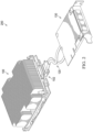
- FIG. 1A is a schematic diagram of a system 100 that includes a substrate diving board 112 and a bolster plate 104 in accordance with embodiments of the present invention.
- a substrate shown in FIG. 1B
- the substrate can include a CPU (not shown) and secured by a Package Heatsink Loading Mechanism (PHLM).
- the substrate can include a substrate diving board 112 that provides an electrical interface to other computing or network elements.
- the LEC assembly interacts with several key components in the system, e.g. substrate diving board and bolster plate 104.
- the physical location of the interface between the LEC assembly and the substrate diving board is where dynamic (mechanical) inputs get magnified significantly. For example, in FIG.
- the plating on the substrate 108 that interfaces with LEC assembly contact is different from other typical edge connectors for other circuits.
- the package/LEC interface is subject to significant system dynamic inputs and is critical to HSIO signal integrity performance. Therefore, the connector assemblies described herein prevent micro-motion / plating wear and fretting by actively retaining the connector with a retaining force (e.g., a force in the range of 13,34 N - 40,03 N).
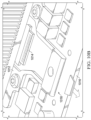
- FIG. 1B is a schematic diagram 170 of a system that includes a mother board 108 and linear edge connector (LEC) assembly 102 in accordance with embodiments of the present disclosure.
- the linear edge connector (LEC) assembly 102 shown in FIG. 1B can be any of the connector assembly embodiments described herein.
- the design space for LEC is strictly constrained by the system layout to clear other components on the board and in the chassis compared to typical edge connectors.
- the form factor of the LEC assembly 102 can accommodate the small spaces available on the mother board 108.
- the form factor of the LEC connector assembly 102 can be on the order of 20mm W (y-direction), 11mm Height (z-direction), and 35mm depth (x-direction).
- the connector assembly uses a latch mechanism that provides active retention force along mating direction by pushing the connector against the substrate. This prevents relative movement between the connector contacts and substrate, and hold the connector in place in the system stack-up.
- Embodiments of this disclosure can be characterized by including bolster plate hard stop feature for retention of a connector assembly.
- bolster plate hard stop feature for retention of a connector assembly.
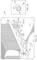
- FIG. 3B is a perspective view of a bolster plate ball in accordance with embodiments of the present disclosure.
- Protrusion 308 can include a ball bearing or similar structure 312 housed in a housing 310.
- the housing 310 can house a spring 314 (not shown) that pushes against the ball bearing 312.
- the ball bearing 312, thus, can be spring loaded in the housing 310.
- Bolster plate protrusion 308 can include a pin or ball bearing or other spherical or substantially spherical element that can be received by a connector assembly (as described further in the sections below).
- the bolster plate protrusion 308 can be located on a bolster plate arm 306 on the bolster plate 302.
- Bolster plate arm 306 can be a protrusion or stamped/inserted elongation extending from the bolster plate 32.
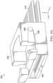
- FIG. 4A is a perspective view of a schematic diagram of a connector assembly 400 in accordance with embodiments of the present disclosure.
- the connector assembly 400 includes a connector body 402 and an electrical interface 404.
- Electrical interface 404 is configured to receive a linear edge connector (LEC) that to electrically connect the contacts on the LEC 322 (of FIG. 3A ) to wires 410 of the connector assembly 400.
- LEC linear edge connector
- the connector body 402 can reside between the electrical interface 404 and the wires 410, and can act as a strain relief for the wires 410.
- the connector body 402 includes a groove 406 configured to receive a bolster plate protrusion, such as the ball 312.
- the groove 406 includes a circular indentation 408.
- the groove 406 and indentation 408 can reside on both sides of the connector body 402.
- the spring 314 in the housing 310 can compress as the ball bearing 312 contacts the surface of the groove 406.
- the spring 314 can push the ball bearing 312 into the indentation 408, which can act as a locking mechanism to retain the connector assembly 400 onto the bolster plate.
- the press fit ball 312 is spring loaded in the center and being utilized as locking feature on bolster plate 302.
- the corresponding groove features 406 on connector work with the press fit ball 312 to lock connector assembly 400 in place and provide movement constrains. Additionally, the groove 406 facilitates self-alignment of the connector assembly 400 to the LEC 322 of FIG. 3A .
- FIG. 4B is a schematic diagram of a connector assembly 400 that is connected to a substrate diving board 322 in accordance with embodiments of the present disclosure.
- the groove features 406 receive the bolster plate protrusion 308, which includes press fit ball 312 located on arm 306 of the bolster plate 302 and connect to two sides of the connector body 402.
- the spring plunger press fit balls 312 go into the groove features 406, the spring loaded balls 312 compress the connector body 402 from two sides in width direction, and the connector assembly 400 will be locked in place and constrained.
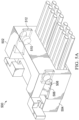
- FIG. 5A is a perspective view of a schematic diagram of a connector assembly 500 in accordance with embodiments of the present disclosure.
- Connector assembly 500 is similar to connector assembly 400.
- connector assembly 500 includes an electrical interface 504 configured to receive a substrate diving board 322.
- the connector body 502 includes a groove 506 that can receive a press fit ball 312 and lock the ball 312 into an indentation 508.
- the connector assembly 500 includes magnet 510.
- Magnet 510 can be over-molded in the connector body 502.
- the magnets 510 can lock the ball 312 in place through an attractive magnetic force.
- the strong magnet attractive force between the magnets 510 embedded and press fit ball 312 on bolster plate 302 can provide very good movement constrain under shipping/operational shock and vibration conditions.
- the press fit ball 312 is not spring loaded.
- the magnetic attraction can be sufficient to secure the connector assembly 500.
- the use of a spring loaded ball can add further compression.
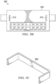
- FIG. 5B is a rear view of a schematic diagram of an embodiment of a connector assembly 500 in accordance with embodiments of the present disclosure.
- the connector body 502 backside includes slots 512.
- the slots 512 are on both sides of the connector body 502.
- FIG. 5C is a schematic diagram of a ferromagnetic key 562 in accordance with embodiments of the present disclosure.
- the ferromagnetic key 562 can have a "U" shaped body, with dimensions conforming to the slots 512 on the connector body 502.
- the "prongs" of the key 562 are long enough to block the magnetic field between the magnets 510 and the ball 312.
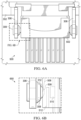
- FIG. 6A is a schematic diagram 600 of a connector assembly 500 that is connected to a bolster plate 302 in accordance with embodiments of the present disclosure.
- FIGS 6B is a close-up view 650 of a bolster plate protrusion 308 in contact with the connector assembly 500 in accordance with embodiments of the present disclosure.
- the groove feature 506 receives the bolster plate protrusion 308, which includes the press fit ball 312 and is located on arm 306 of the bolster plate 302 and connect to two sides of the connector body 402.
- the press fit balls 312 compress the connector body 402 from two sides in width direction.
- the press fit ball 312 can then be received into the indentation 508.
- FIG. 8 is a schematic diagram of a connector assembly in accordance with embodiments of the present disclosure.
- the linear edge connector (LEC) assembly 802 includes a connector body 804 and an electrical interface 806.
- the connector body 804 and the electrical interface 806 include a plastic molded track system 808 incorporated on each side of the connector assembly 802.
- a stamped metal leaf spring 810 is incorporated into the track system 808.
- the track 808 and leaf spring 810 act as a guide while installing the connector 802.
- the leaf spring 810 snaps to the bolster-plate ball 312 when fully inserted to lock the connector 802 in place.
- the bolster plate ball 312 can slide through the track system 808 during connection with the substrate diving board. Toward the end of travel, the ball 312 can overcome the arc-shape clamp feature 810 of leaf spring 812 and be locked in place at the end of the track system 808. Correspondingly, the connector 802 will be able to firmly grab on the ball features 312 and be locked to bolster plate. Since the bolster plate is a more rigid component in the stack-up and is part of the PHLM mechanism that the substrate is attached to, the movement of the connector 802 relative to substrate can be effectively controlled.
- the connector assembly 802 includes a lever 814 connected to the leaf spring 810.
- the connector 802 is released from the bolster plate by pinching the lever 814 and connector body 802 together, thus disengaging the leaf spring 810 from the bolster plate ball 312.
- the connector can be slide backwards with less resistance.
- FIG. 9A is a schematic diagram of a connector assembly 900 in accordance with embodiments of the present disclosure.
- Connector assembly 900 includes magnetic rods 904 over molded in the connector body 902.
- the bolster plate includes magnetic/ferrous hard stop feature 914 on bolster plate 912 to lock the connector assembly 900 in place.
- the strong attraction force directly along connector/substrate mating direction (x-direction) will constrain connector movement under shock/vibration conditions.
- FIG. 9B is a schematic diagram of a connector assembly 900 connected to a substrate diving board 916.
- a magnetic/ferrous hard stop feature 914 is incorporated in bolster plate 912.
- the attraction force between the magnetic strips 904 and the magnetic/ferrous hard stop feature 914 increases.
- the connector 900 will automatically align with the magnetic/ferrous hard stop feature 914 due to the strong magnetic force (approximate 19,13 N).
- FIG. 10B is a schematic diagram of a bolster plate 1012.
- a push ball/screw retention slot 1016 is built into a receiving plate 1018 of the bolster plate 1012 located above the mother board.
- the retention slot 1016 can be aligned to receive the connection assembly push ball / screw 1006 and ensure that the electrical interface 1004 can receive the diving board 1014.
- the push-ball/screw 1006 can be pushed/ screwed through the hole on connector body 1002 and lock the connector to the slot on bolster plate 1012. As mentioned before, by locking the connector assembly 1000 to the bolster plate 1012, the relative movement between substrate and connector can be well controlled.
- the push-ball retention mechanism By locking the connector firmly (relatively large contact area) to the bolster plate 1012, the push-ball retention mechanism can provide very good movement constraint on connector assembly 1000.
- the push-ball/screw retention mechanism can also help with strain relief under various cable use condition, e.g. in-plane bend, out-of-plane bend, etc, to isolate the connector inner feature to external load.
- the external load By fixing the connector assembly 1000 to bolster plate 1012, the external load can be transferred to relative rigid bolster plate through push-ball mechanism so that the connector inner features, e.g., solder joints, contacts, etc. can be protected.
- FIG. 11 is a block diagram of an example computing device 1100 that may connected via a linear edge connector.
- the computing device 1100 may include one or more processors 1102 (e.g., one or more processor cores implemented on one or more components) and a system memory 1104 (implemented on one or more components).
- processors 1102 e.g., one or more processor cores implemented on one or more components
- system memory 1104 implemented on one or more components
- the term "processor” or “processing device” may refer to any device or portion of a device that processes electronic data from registers and/or memory to transform that electronic data into other electronic data that may be stored in registers and/or memory.
- the processor(s) 1102 may include one or more microprocessors, graphics processors, digital signal processors, crypto processors, or other suitable devices. More generally, the computing device 1100 may include any suitable computational circuitry, such as one or more Application Specific Integrated Circuits (ASICs).
- ASICs Application Specific Integrated Circuits
- the computing device 1100 may include one or more mass storage devices 1106 (such as flash memory devices or any other mass storage device suitable for inclusion in a flexible IC package).
- the system memory 1104 and the mass storage device 1106 may include any suitable storage devices, such as volatile memory (e.g., dynamic random access memory (DRAM)), nonvolatile memory (e.g., read-only memory (ROM)), and flash memory.
- the computing device 1100 may include one or more I/O devices 1108 (such as display, user input device, network interface cards, modems, and so forth, suitable for inclusion in a flexible IC device).
- the elements may be coupled to each other via a system bus 1112, which represents one or more buses.
- system memory 1104 and the mass storage device 1106 may be employed to store a working copy and a permanent copy of programming instructions 1122.
- Machine-accessible media including non-transitory computer-readable storage media
- methods, systems, and devices for performing the above-described techniques are illustrative examples of embodiments disclosed herein for a linear edge connector.
- a computer-readable media e.g., the system memory 1104 and/or the mass storage device 1106
- may have stored thereon instructions e.g., the instructions 1122
Landscapes
- Engineering & Computer Science (AREA)
- Theoretical Computer Science (AREA)
- Manufacturing & Machinery (AREA)
- Microelectronics & Electronic Packaging (AREA)
- Computer Hardware Design (AREA)
- Power Engineering (AREA)
- Human Computer Interaction (AREA)
- Physics & Mathematics (AREA)
- General Engineering & Computer Science (AREA)
- General Physics & Mathematics (AREA)
- Details Of Connecting Devices For Male And Female Coupling (AREA)
Description
- This application claims priority to
U.S. Patent Application No. 15/084,726, filed March 30, 2016 and titled "LINEAR EDGE CONNECTOR RETENTION". - This disclosure pertains to linear edge connector retention mechanisms.
- Linear Edge Connectors (LEC) are part of an Internal Faceplate-to-Processor (IFP) internal cable which enables high speed, low loss data direct connection from a processor to an fabric network. On one end of the IFP cable can be a 54-ball LEC that connects to a processor package. On the other end of the IFP cable, two 28-pins plugs can mate to Internal Faceplate Transition Connector (IFT connector).
- The inherent nature of direct connection to a CPU board for LEC determines its fine contact pitch and tight tolerance, which differentiate LEC from other available edge connectors. Document
US 2009 197431 A1 describes an electrical connector for receiving an electrical card assembly. -
-
FIG. 1A is a schematic diagram of a central processing unit board that includes a substrate diving board in accordance with embodiments of the present disclosure. -
FIG 1B is a schematic diagram of a central processing unit board that includes a linear edge connector assembly connected to a substrate diving board in accordance with embodiments of the present disclosure. -
FIG. 2 is a schematic diagram of central processing unit board connected to another board by a cable assembly in accordance with embodiments of the present disclosure. -
FIG. 3A is a perspective view of a schematic diagram of a bolster plate in accordance with embodiments of the present disclosure. -
FIG. 3B is a close-up view of a bolster plate protrusion in accordance with embodiments of the present disclosure. -
FIG. 4A is a perspective view of a schematic diagram of a connector assembly in accordance with embodiments of the present disclosure. -
FIG. 4B is a schematic diagram of a connector assembly that is connected to a substrate diving board in accordance with embodiments of the present disclosure. -
FIG. 5A is a perspective view of a schematic diagram of a connector assembly in accordance with embodiments of the present disclosure. -
FIG. 5B is a rear view of a schematic diagram of an embodiment of a connector assembly in accordance with embodiments of the present disclosure. -
FIG. 5C is a schematic diagram of a ferromagnetic key in accordance with embodiments of the present disclosure. -
FIG. 6A is a schematic diagram of a connector assembly that is connected to a bolster plate in accordance with embodiments of the present disclosure. -
FIGS 6B is a close-up view of a bolster plate ball in contact with the connector assembly in accordance with embodiments of the present disclosure. -
FIG. 7A is a schematic diagram of a connector assembly attached to a bolster playe in accordance with embodiments of the present disclosure. -
FIG. 7B a close-up view of a connector assembly connected to a bolster plate ball in accordance with embodiments of the present disclosure. -
FIG. 8 is a schematic diagram of a connector assembly in accordance with embodiments of the present disclosure. -
FIG. 9A is a schematic diagram of a connector assembly in accordance with embodiments of the present disclosure. -
FIG. 9B is a schematic diagram of a connector assembly in connection with a substrate diving board in accordance with embodiments of the present disclosure. -
FIG. 10A is a schematic diagram of a connector assembly connected to a substrate diving board and bolster plate. -
FIG. 10B is a schematic diagram of a bolster plate. -
FIG. 11 is a block diagram of an example computing device that may connected via a linear edge connector - This disclosure describes embodiments of a linear edge connector (LEC) assembly for connecting a cable bundle to a substrate diving board that can carry a central processing unit and/or other computer component. In embodiments, a bolster plate includes structural elements to provide structural support for connecting the LEC assembly to substrate diving board. Embodiments of the disclosure are also directed to securing the cable bundle to the LEC with sufficient force to prevent LEC electrical failure through shipping vibration induced fretting.
- Retention mechanisms can add to functionality of Linear Edge Connector for fabric version of server products. For edge connectors, fretting corrosion is a common issue caused by micro-movement of the connector contact tip relative to substrate diving board pad under shipping/operational shock and shipping vibration conditions. It is a potential risk for connector electrical performance.
-
FIG. 1A is a schematic diagram of asystem 100 that includes asubstrate diving board 112 and abolster plate 104 in accordance with embodiments of the present invention. A substrate (shown inFIG. 1B ) can include a CPU (not shown) and secured by a Package Heatsink Loading Mechanism (PHLM). The substrate can include asubstrate diving board 112 that provides an electrical interface to other computing or network elements. At the system stack level, the LEC assembly interacts with several key components in the system, e.g. substrate diving board andbolster plate 104. The physical location of the interface between the LEC assembly and the substrate diving board is where dynamic (mechanical) inputs get magnified significantly. For example, inFIG. 1A , asubstrate 108 is attached to a heat sink 110 (through the PHLM), which plays a big role in dynamic input. Also, to accommodate routing options for different system layouts and provide flexibility for customers, the cable bundle is not retained on the mother board which further magnifies the dynamic inputs on LEC assembly during shipping (shock and vibration). - Additionally, the plating on the
substrate 108 that interfaces with LEC assembly contact is different from other typical edge connectors for other circuits. The package/LEC interface is subject to significant system dynamic inputs and is critical to HSIO signal integrity performance. Therefore, the connector assemblies described herein prevent micro-motion / plating wear and fretting by actively retaining the connector with a retaining force (e.g., a force in the range of 13,34 N - 40,03 N). -
FIG. 1B is a schematic diagram 170 of a system that includes amother board 108 and linear edge connector (LEC)assembly 102 in accordance with embodiments of the present disclosure. The linear edge connector (LEC)assembly 102 shown inFIG. 1B can be any of the connector assembly embodiments described herein. Of note inFIG. 1B is the limited clearance available for connecting the linear edge connector assembly to the bolster plate and substrate diving board. The design space for LEC is strictly constrained by the system layout to clear other components on the board and in the chassis compared to typical edge connectors. The form factor of theLEC assembly 102 can accommodate the small spaces available on themother board 108. For example, the form factor of theLEC connector assembly 102 can be on the order of 20mm W (y-direction), 11mm Height (z-direction), and 35mm depth (x-direction). -
FIG. 2 is a schematic diagram of central processing unit board connected to another board by a cable assembly in accordance with embodiments of the present disclosure. - The aforementioned factors lay great challenges on LEC retention mechanism design to retain connector in place and prevent plating wear and fretting under use/ shipping conditions. This disclosure describes embodiments for connector assemblies having the following general characteristics:
- Each can lock the connector to a rigid component on the CPU package;
- Each can constrain translation/rotation in all directions; and
- Each includes an active retention force between package diving board and the connector assembly.
- In embodiments, the connector assembly uses a latch mechanism that provides active retention force along mating direction by pushing the connector against the substrate. This prevents relative movement between the connector contacts and substrate, and hold the connector in place in the system stack-up.
- The following retention mechanism designs are proposed here to solve the aforementioned fretting issue. Embodiments of this disclosure can be characterized by including bolster plate hard stop feature for retention of a connector assembly. Among the embodiments of this disclosure are:
- 1. Press fit ball retention mechanism design
- 3. Magnetic/Ferrous connector hard stop retention mechanism
- 2. Ball-track latch retention mechanism
- 4. Push-ball/Screw retention mechanism design (not claimed but useful for understanding the invention)
-
FIG. 3A is a perspective view of a schematic diagram 300 of a bolsterplate 302 in accordance with embodiments of the present disclosure. Bolsterplate 302 can be similar to that of bolsterplate 104 shown inFIG. 1A . Thesubstrate diving board 322 can include electrical contacts for connecting electrical elements on the CPU package with external elements and/or devices through a connector assembly. The bolsterplate 302 can include bolsterplate arm 306 that can hold a bolsterplate protrusion 308.FIG. 3A shows an example of a bolsterplate protrusion 308 for receiving a connector assembly in accordance with embodiments of the present disclosure.FIG. 3A also shows thesubstrate diving board 322. Thesubstrate diving board 322 includes one or more electrical contacts that electrically connect substrate elements (such as a CPU) to external elements, through the LEC assembly. -
FIG. 3B is a perspective view of a bolster plate ball in accordance with embodiments of the present disclosure.Protrusion 308 can include a ball bearing orsimilar structure 312 housed in ahousing 310. In some embodiments, thehousing 310 can house a spring 314 (not shown) that pushes against theball bearing 312. Theball bearing 312, thus, can be spring loaded in thehousing 310. Bolsterplate protrusion 308 can include a pin or ball bearing or other spherical or substantially spherical element that can be received by a connector assembly (as described further in the sections below). The bolsterplate protrusion 308 can be located on a bolsterplate arm 306 on the bolsterplate 302. Bolsterplate arm 306 can be a protrusion or stamped/inserted elongation extending from the bolster plate 32. -
FIG. 4A is a perspective view of a schematic diagram of aconnector assembly 400 in accordance with embodiments of the present disclosure. Theconnector assembly 400 includes aconnector body 402 and anelectrical interface 404.Electrical interface 404 is configured to receive a linear edge connector (LEC) that to electrically connect the contacts on the LEC 322 (ofFIG. 3A ) towires 410 of theconnector assembly 400. - The
connector body 402 can reside between theelectrical interface 404 and thewires 410, and can act as a strain relief for thewires 410. Theconnector body 402 includes agroove 406 configured to receive a bolster plate protrusion, such as theball 312. Thegroove 406 includes acircular indentation 408. Thegroove 406 andindentation 408 can reside on both sides of theconnector body 402. Thespring 314 in thehousing 310 can compress as theball bearing 312 contacts the surface of thegroove 406. Thespring 314 can push theball bearing 312 into theindentation 408, which can act as a locking mechanism to retain theconnector assembly 400 onto the bolster plate. - The press
fit ball 312 is spring loaded in the center and being utilized as locking feature on bolsterplate 302. The corresponding groove features 406 on connector work with the pressfit ball 312 to lockconnector assembly 400 in place and provide movement constrains. Additionally, thegroove 406 facilitates self-alignment of theconnector assembly 400 to theLEC 322 ofFIG. 3A . -
FIG. 4B is a schematic diagram of aconnector assembly 400 that is connected to asubstrate diving board 322 in accordance with embodiments of the present disclosure. The groove features 406 receive the bolsterplate protrusion 308, which includes pressfit ball 312 located onarm 306 of the bolsterplate 302 and connect to two sides of theconnector body 402. When the spring plunger pressfit balls 312 go into the groove features 406, the spring loadedballs 312 compress theconnector body 402 from two sides in width direction, and theconnector assembly 400 will be locked in place and constrained. -
FIG. 5A is a perspective view of a schematic diagram of aconnector assembly 500 in accordance with embodiments of the present disclosure.Connector assembly 500 is similar toconnector assembly 400. For example,connector assembly 500 includes anelectrical interface 504 configured to receive asubstrate diving board 322. Theconnector body 502 includes agroove 506 that can receive a pressfit ball 312 and lock theball 312 into anindentation 508. - The
connector assembly 500 includesmagnet 510.Magnet 510 can be over-molded in theconnector body 502. Themagnets 510 can lock theball 312 in place through an attractive magnetic force. The strong magnet attractive force between themagnets 510 embedded and pressfit ball 312 on bolsterplate 302 can provide very good movement constrain under shipping/operational shock and vibration conditions. - In some embodiments, the press
fit ball 312 is not spring loaded. The magnetic attraction can be sufficient to secure theconnector assembly 500. The use of a spring loaded ball can add further compression. - The
connector assembly 500 can include aslot 512 that creates a cavity between themagnet 510 and the side of theconnector body 502. Theslot 512 can receive a ferromagnetic element (shown inFIG. 5C ) to block the magnetic field between themagnet 510 and theball 312. -
FIG. 5B is a rear view of a schematic diagram of an embodiment of aconnector assembly 500 in accordance with embodiments of the present disclosure. Theconnector body 502 backside includesslots 512. Theslots 512 are on both sides of theconnector body 502.FIG. 5C is a schematic diagram of aferromagnetic key 562 in accordance with embodiments of the present disclosure. Theferromagnetic key 562 can have a "U" shaped body, with dimensions conforming to theslots 512 on theconnector body 502. The "prongs" of the key 562 are long enough to block the magnetic field between themagnets 510 and theball 312. -
FIG. 6A is a schematic diagram 600 of aconnector assembly 500 that is connected to a bolsterplate 302 in accordance with embodiments of the present disclosure.FIGS 6B is a close-upview 650 of a bolsterplate protrusion 308 in contact with theconnector assembly 500 in accordance with embodiments of the present disclosure. Thegroove feature 506 receives the bolsterplate protrusion 308, which includes the pressfit ball 312 and is located onarm 306 of the bolsterplate 302 and connect to two sides of theconnector body 402. When theball 312 fits into thegroove feature 506 and theindentation 508, the pressfit balls 312 compress theconnector body 402 from two sides in width direction. The pressfit ball 312 can then be received into theindentation 508.Indentation 508 is proximate to themagnet 510. When theball 312 is received into theindentation 508, the magnetic attraction between themagnet 510 and theball 312 can lock and constrain theconnector assembly 500. Theslot 512 in theconnector body 502 creates a cavity between themagnet 510 and theball 312. Absent the ferromagnetic key, the magnetic field created by themagnet 510 can secure theball 312. -
FIG. 7A is a schematic diagram 700 of aconnector assembly 500 attached to a bolsterplate 302 in accordance with embodiments of the present disclosure.FIG. 7B a close-upview 750 of aconnector assembly 500 connected to a bolsterplate protrusion 308 in accordance with embodiments of the present disclosure. Theconnector body 502 includes aferromagnetic key 562 received within theslots 512. Theferromagnetic key 562 can block the magnetic field from themagnet 510, thereby permitting the connector to be removed without the counter active magnetic force. To remove the connector from assembly, a ferromagnetic key can be inserted into connector back-shell to block the magnetic field and release the magnet attraction force. -
FIG. 8 is a schematic diagram of a connector assembly in accordance with embodiments of the present disclosure. The linear edge connector (LEC)assembly 802 includes aconnector body 804 and anelectrical interface 806. Theconnector body 804 and theelectrical interface 806 include a plastic moldedtrack system 808 incorporated on each side of theconnector assembly 802. A stampedmetal leaf spring 810 is incorporated into thetrack system 808. Thetrack 808 andleaf spring 810 act as a guide while installing theconnector 802. Theleaf spring 810 snaps to the bolster-plate ball 312 when fully inserted to lock theconnector 802 in place. - The bolster
plate ball 312 can slide through thetrack system 808 during connection with the substrate diving board. Toward the end of travel, theball 312 can overcome the arc-shape clamp feature 810 ofleaf spring 812 and be locked in place at the end of thetrack system 808. Correspondingly, theconnector 802 will be able to firmly grab on the ball features 312 and be locked to bolster plate. Since the bolster plate is a more rigid component in the stack-up and is part of the PHLM mechanism that the substrate is attached to, the movement of theconnector 802 relative to substrate can be effectively controlled. - To release the
connector 802 from the locked position, theconnector assembly 802 includes alever 814 connected to theleaf spring 810. Theconnector 802 is released from the bolster plate by pinching thelever 814 andconnector body 802 together, thus disengaging theleaf spring 810 from the bolsterplate ball 312. The connector can be slide backwards with less resistance. -
FIG. 9A is a schematic diagram of aconnector assembly 900 in accordance with embodiments of the present disclosure.Connector assembly 900 includesmagnetic rods 904 over molded in theconnector body 902. The bolster plate includes magnetic/ferrous hard stop feature 914 on bolsterplate 912 to lock theconnector assembly 900 in place. The strong attraction force directly along connector/substrate mating direction (x-direction) will constrain connector movement under shock/vibration conditions. -
FIG. 9B is a schematic diagram of aconnector assembly 900 connected to asubstrate diving board 916. A magnetic/ferrous hard stop feature 914 is incorporated in bolsterplate 912. As the connector is being plugged on the packagesubstrate diving board 916, the attraction force between themagnetic strips 904 and the magnetic/ferrous hard stop feature 914 increases. As the distance between the connector and bolster plate hard stop feature further decreases, theconnector 900 will automatically align with the magnetic/ferrous hard stop feature 914 due to the strong magnetic force (approximate 19,13 N). -
FIG. 10A is a schematic diagram of aconnector assembly 1000. Theconnector assembly 1000 can include aconnector body 1002 and anelectrical interface 1004. Theelectrical interface 1004 can receive asubstrate diving board 1014 and electrically connect the contacts on thesubstrate diving board 1014 to conductors in a cable assembly. Theconnector body 1002 can include a retention slot through theconnector body 1002. A press ball/screw 1006 can be pushed/screwed into the slots ofconnector body 1002 and areceiver plate 1018 of the bolsterplate 1012 to retain the connector in place. -
FIG. 10B is a schematic diagram of a bolsterplate 1012. To facilitate the movement constraint on theconnector assembly 1000 ofFIG. 10A , a push ball/screw retention slot 1016 is built into a receivingplate 1018 of the bolsterplate 1012 located above the mother board. Theretention slot 1016 can be aligned to receive the connection assembly push ball /screw 1006 and ensure that theelectrical interface 1004 can receive thediving board 1014. - After engaging the connector with substrate diving board, the push-ball/
screw 1006 can be pushed/ screwed through the hole onconnector body 1002 and lock the connector to the slot on bolsterplate 1012. As mentioned before, by locking theconnector assembly 1000 to the bolsterplate 1012, the relative movement between substrate and connector can be well controlled. - By locking the connector firmly (relatively large contact area) to the bolster
plate 1012, the push-ball retention mechanism can provide very good movement constraint onconnector assembly 1000. The push-ball/screw retention mechanism can also help with strain relief under various cable use condition, e.g. in-plane bend, out-of-plane bend, etc, to isolate the connector inner feature to external load. By fixing theconnector assembly 1000 to bolsterplate 1012, the external load can be transferred to relative rigid bolster plate through push-ball mechanism so that the connector inner features, e.g., solder joints, contacts, etc. can be protected. -
FIG. 11 is a block diagram of anexample computing device 1100 that may connected via a linear edge connector. As shown, thecomputing device 1100 may include one or more processors 1102 (e.g., one or more processor cores implemented on one or more components) and a system memory 1104 (implemented on one or more components). As used herein, the term "processor" or "processing device" may refer to any device or portion of a device that processes electronic data from registers and/or memory to transform that electronic data into other electronic data that may be stored in registers and/or memory. The processor(s) 1102 may include one or more microprocessors, graphics processors, digital signal processors, crypto processors, or other suitable devices. More generally, thecomputing device 1100 may include any suitable computational circuitry, such as one or more Application Specific Integrated Circuits (ASICs). - The
computing device 1100 may include one or more mass storage devices 1106 (such as flash memory devices or any other mass storage device suitable for inclusion in a flexible IC package). Thesystem memory 1104 and themass storage device 1106 may include any suitable storage devices, such as volatile memory (e.g., dynamic random access memory (DRAM)), nonvolatile memory (e.g., read-only memory (ROM)), and flash memory. Thecomputing device 1100 may include one or more I/O devices 1108 (such as display, user input device, network interface cards, modems, and so forth, suitable for inclusion in a flexible IC device). The elements may be coupled to each other via asystem bus 1112, which represents one or more buses. - Each of these elements may perform its conventional functions known in the art. In particular, the
system memory 1104 and themass storage device 1106 may be employed to store a working copy and a permanent copy ofprogramming instructions 1122. - The permanent copy of the
programming instructions 1122 may be placed into permanentmass storage devices 1106 in the factory or through a communication device included in the I/O devices 1108 (e.g., from a distribution server (not shown)). The constitution of elements 1102-1112 are known, and accordingly will not be further described. - Machine-accessible media (including non-transitory computer-readable storage media), methods, systems, and devices for performing the above-described techniques are illustrative examples of embodiments disclosed herein for a linear edge connector. For example, a computer-readable media (e.g., the
system memory 1104 and/or the mass storage device 1106) may have stored thereon instructions (e.g., the instructions 1122) such that, when the instructions are executed by one or more of theprocessors 1102. - The relative sizes of features shown in the figures are not drawn to scale.
Claims (12)
- A linear edge connector assembly (400, 500) comprising:an electrical interface (404) configured to receive a substrate diving board (322) and electrically couple the substrate diving board with a conductor of a cable bundle (410), anda retention mechanism body (402) coupled to the electrical interface (404), the retention mechanism body (402) comprising:a bolster plate receiving groove (406) to receive a protrusion (308) on a bolster plate (302) mechanically connected to the substrate diving board, anda bolster plate receiving indentation (408) to receive the bolster plate protrusion.
- The connector assembly of claim 1, wherein the bolster plate receiving indentation (408) comprises a circular indentation to receive a circular protrusion on the bolster plate.
- The connector assembly of claim 1, wherein the retention mechanism body (402) comprises a magnetic element (510) to magnetically couple the bolster plate protrusion to the retention mechanism body (402).
- The connector assembly of claim 3, wherein the retention mechanism body (402) comprises a backwall that comprises a slot (512) configured to receive a ferromagnetic rod, the slot defining a cavity between the magnetic element and the bolster plate receiving indentation (408).
- The connector assembly of claim 1, wherein the bolster plate protrusion comprises a spring loaded ball bearing (312).
- A linear edge connector assembly (802) comprising:an electrical interface (806) configured to receive a substrate diving board and electrically couple the substrate diving board with a conductor of a cable bundle, anda retention mechanism body (804) coupled to the electrical interface (806),the retention mechanism body (402) comprising:a bolster plate receiving track (808) to receive a protrusion on a bolster plate mechanically connected to the substrate diving board, anda leaf spring (810) comprising a curved portion (812), the curved portion reducing a width of the track and configured to confine the bolster plate protrusion.
- The connector assembly of claim 6, further comprising a release spring coupled to the leaf spring (810), the release spring (814) configured to apply a force on the leaf spring to release the bolster plate protrusion.
- The connector assembly of claim 7, wherein the release spring is configured to be squeezed against the retention mechanism body (804) to release the bolster plate protrusion.
- A linear edge connector assembly (900) comprising:an electrical interface (906) configured to receive a substrate diving board (916) and electrically couple the substrate diving board with a conductor of a cable bundle, anda retention mechanism body (902) coupled to the electrical interface (906), the retention mechanism body (902) comprising:a magnetic element (904) residing within the retention mechanism body (902), the magnetic element (904) configured to magnetically attract a magnetic hard stop feature (914)on a bolster plate (912) mechanically connected to the substrate diving board.
- The connector assembly of claim 9, wherein the retention mechanism body (902) comprises a plurality of magnetic elements.
- The connector assembly of claim 9 or 10, wherein the magnetic element is over-molded in the retention mechanism body (902).
- A computing system (1100) comprising:a central processing unit, CPU, (1102) residing on a substrate, the substrate comprising a diving board (112) comprising contacts coupled to the CPU (1102);a bolster plate (104) mechanically connected to the substrate, the bolster plate (104) comprising a connector receiving element (306) comprising a protrusion (308); anda linear edge connector assembly (400, 500, 800, 900) according to one of the previous claims
Applications Claiming Priority (2)
| Application Number | Priority Date | Filing Date | Title |
|---|---|---|---|
| US15/084,726 US9825387B2 (en) | 2016-03-30 | 2016-03-30 | Linear edge connector with a cable retention mechanism having a body with a groove with an indentation to receive a bolster plate protrusion |
| PCT/US2017/020023 WO2017172191A1 (en) | 2016-03-30 | 2017-02-28 | Linear edge connector retention |
Publications (3)
| Publication Number | Publication Date |
|---|---|
| EP3437164A1 EP3437164A1 (en) | 2019-02-06 |
| EP3437164A4 EP3437164A4 (en) | 2019-11-20 |
| EP3437164B1 true EP3437164B1 (en) | 2023-11-15 |
Family
ID=59959772
Family Applications (1)
| Application Number | Title | Priority Date | Filing Date |
|---|---|---|---|
| EP17776196.2A Active EP3437164B1 (en) | 2016-03-30 | 2017-02-28 | Linear edge connector retention |
Country Status (4)
| Country | Link |
|---|---|
| US (1) | US9825387B2 (en) |
| EP (1) | EP3437164B1 (en) |
| CN (1) | CN108701940A (en) |
| WO (1) | WO2017172191A1 (en) |
Families Citing this family (6)
| Publication number | Priority date | Publication date | Assignee | Title |
|---|---|---|---|---|
| US10680367B2 (en) * | 2016-03-30 | 2020-06-09 | Intel Corporation | Cable retention assemblies including torsional elements |
| CN207720526U (en) * | 2017-11-06 | 2018-08-10 | 华为技术有限公司 | Single-plate component and electronic equipment |
| US10873161B2 (en) * | 2019-05-06 | 2020-12-22 | Te Connectivity Corporation | Receptacle assembly having cabled receptacle connector |
| US10873160B2 (en) | 2019-05-06 | 2020-12-22 | Te Connectivity Corporation | Receptacle assembly having cabled receptacle connector |
| WO2021183841A1 (en) * | 2020-03-13 | 2021-09-16 | Samtec, Inc. | Cable connector system |
| CN113675154B (en) * | 2020-05-13 | 2024-11-15 | 华为技术有限公司 | Chip modules and electronic devices |
Family Cites Families (24)
| Publication number | Priority date | Publication date | Assignee | Title |
|---|---|---|---|---|
| DE3103455C2 (en) * | 1981-02-02 | 1984-03-22 | Siemens AG, 1000 Berlin und 8000 München | Electrical connector, in particular for data technology |
| JP3658080B2 (en) * | 1996-04-16 | 2005-06-08 | 富士通コンポーネント株式会社 | connector |
| US6383000B1 (en) * | 1999-11-01 | 2002-05-07 | Delaware Capital Formation, Inc. | Electrical conductivity assembly for swivel arms |
| US6415168B1 (en) * | 2000-04-19 | 2002-07-02 | Ad-Tech Medical Instrument Corporation | Electrical connector for multi-contact medical electrodes |
| US6771511B2 (en) | 2002-04-22 | 2004-08-03 | Optical Communication Products, Inc. | Pluggable optical transceiver with pivoting actuator lever |
| US7232332B2 (en) * | 2003-01-07 | 2007-06-19 | Sun Microsystems, Inc. | Support and grounding structure |
| US6887090B2 (en) | 2003-07-25 | 2005-05-03 | Hon Hai Precision Ind. Co., Ltd. | Electrical connector with retention clip |
| US6830472B1 (en) * | 2003-09-10 | 2004-12-14 | Hon Hai Precision Ind. Co., Ltd. | Cable end connector assembly having locking member |
| US6920274B2 (en) * | 2003-12-23 | 2005-07-19 | Adc Telecommunications, Inc. | High density optical fiber distribution frame with modules |
| JP4458239B2 (en) | 2003-12-26 | 2010-04-28 | 日本電気株式会社 | Unlocking mechanism, optical module, and unlocking method |
| US7160126B1 (en) * | 2005-09-06 | 2007-01-09 | Giga-Byte Technology Co., Ltd. | Printed circuit board connector with locking device |
| US7189098B1 (en) * | 2005-12-30 | 2007-03-13 | Hon Hai Precision Ind. Co., Ltd. | Cable connector assembly and method of manufacturing the same |
| US7467948B2 (en) * | 2006-06-08 | 2008-12-23 | Nokia Corporation | Magnetic connector for mobile electronic devices |
| JP2008233645A (en) | 2007-03-22 | 2008-10-02 | Fujitsu Ltd | Optical module |
| US7762817B2 (en) * | 2008-01-04 | 2010-07-27 | Apple Inc. | System for coupling interfacing parts |
| CN201178181Y (en) | 2008-02-01 | 2009-01-07 | 富士康(昆山)电脑接插件有限公司 | electrical connector |
| JP5080336B2 (en) * | 2008-04-04 | 2012-11-21 | 日本航空電子工業株式会社 | Board mounting connector |
| CN201523097U (en) * | 2009-09-17 | 2010-07-07 | 富士康(昆山)电脑接插件有限公司 | electrical connector |
| US9065205B2 (en) | 2011-08-11 | 2015-06-23 | Apple Inc. | Connector insert having a cable crimp portion with protrusions and a receptacle having label in the front |
| US9545040B2 (en) | 2012-01-23 | 2017-01-10 | Fci Americas Technology Llc | Cable retention housing |
| US9048651B2 (en) | 2013-02-05 | 2015-06-02 | Bose Corporation | Low-profile strain relief and cable retention |
| JP2015050033A (en) * | 2013-09-02 | 2015-03-16 | 株式会社島野製作所 | Socket plug mechanism |
| TWM494440U (en) | 2014-04-02 | 2015-01-21 | Hon Hai Prec Ind Co Ltd | Protection cap and retention member having the same |
| TW201541136A (en) | 2014-04-23 | 2015-11-01 | Foxconn Interconnect Technology Ltd | Retention module |
-
2016
- 2016-03-30 US US15/084,726 patent/US9825387B2/en not_active Expired - Fee Related
-
2017
- 2017-02-28 EP EP17776196.2A patent/EP3437164B1/en active Active
- 2017-02-28 CN CN201780013730.7A patent/CN108701940A/en active Pending
- 2017-02-28 WO PCT/US2017/020023 patent/WO2017172191A1/en not_active Ceased
Also Published As
| Publication number | Publication date |
|---|---|
| EP3437164A4 (en) | 2019-11-20 |
| US20170288331A1 (en) | 2017-10-05 |
| WO2017172191A1 (en) | 2017-10-05 |
| EP3437164A1 (en) | 2019-02-06 |
| CN108701940A (en) | 2018-10-23 |
| US9825387B2 (en) | 2017-11-21 |
Similar Documents
| Publication | Publication Date | Title |
|---|---|---|
| US9825387B2 (en) | Linear edge connector with a cable retention mechanism having a body with a groove with an indentation to receive a bolster plate protrusion | |
| US7699644B2 (en) | Electrical connector with protective member | |
| KR101625745B1 (en) | Circuit-terminal connecting device | |
| US8837135B2 (en) | Expansion module for interface card, computer case assembly, and computer system | |
| US5779494A (en) | Connector with reinforced latch | |
| US9270042B2 (en) | Card connector | |
| US6824413B1 (en) | Electrical connector with retention mechanism | |
| US6394831B1 (en) | Retention member for card edge connector | |
| US10680367B2 (en) | Cable retention assemblies including torsional elements | |
| TW202130062A (en) | Connector | |
| US9048553B2 (en) | Card socket with heat sink | |
| US5151041A (en) | Device for connecting and disconnecting first and second electrical connector parts | |
| US20230028263A1 (en) | Card retainers | |
| US20070190817A1 (en) | Card Connector | |
| JP6281698B2 (en) | Connector device | |
| US9209564B2 (en) | Card connector | |
| JP7832246B2 (en) | Staggered paddle card connector | |
| JP2002505779A (en) | Protection card for IC card slot | |
| US20010008815A1 (en) | IC card connector | |
| CN120814118A (en) | Robust miniaturization FFC connector of (C) | |
| US20200099150A1 (en) | Mechanical spring diode contact | |
| JP2005050790A (en) | Improved switch terminal for memory card connector | |
| US20130078862A1 (en) | Card edge connector | |
| US20040242047A1 (en) | System and method for mounting a processor | |
| US20120231656A1 (en) | Connector fixation metal fitting and connector |
Legal Events
| Date | Code | Title | Description |
|---|---|---|---|
| STAA | Information on the status of an ep patent application or granted ep patent |
Free format text: STATUS: THE INTERNATIONAL PUBLICATION HAS BEEN MADE |
|
| PUAI | Public reference made under article 153(3) epc to a published international application that has entered the european phase |
Free format text: ORIGINAL CODE: 0009012 |
|
| STAA | Information on the status of an ep patent application or granted ep patent |
Free format text: STATUS: REQUEST FOR EXAMINATION WAS MADE |
|
| 17P | Request for examination filed |
Effective date: 20180829 |
|
| AK | Designated contracting states |
Kind code of ref document: A1 Designated state(s): AL AT BE BG CH CY CZ DE DK EE ES FI FR GB GR HR HU IE IS IT LI LT LU LV MC MK MT NL NO PL PT RO RS SE SI SK SM TR |
|
| AX | Request for extension of the european patent |
Extension state: BA ME |
|
| DAV | Request for validation of the european patent (deleted) | ||
| DAX | Request for extension of the european patent (deleted) | ||
| A4 | Supplementary search report drawn up and despatched |
Effective date: 20191017 |
|
| RIC1 | Information provided on ipc code assigned before grant |
Ipc: H01R 13/639 20060101ALI20191011BHEP Ipc: H01R 107/00 20060101ALI20191011BHEP Ipc: H01R 12/77 20110101ALI20191011BHEP Ipc: G06F 1/18 20060101AFI20191011BHEP |
|
| STAA | Information on the status of an ep patent application or granted ep patent |
Free format text: STATUS: EXAMINATION IS IN PROGRESS |
|
| 17Q | First examination report despatched |
Effective date: 20211108 |
|
| REG | Reference to a national code |
Ref country code: DE Ref legal event code: R079 Free format text: PREVIOUS MAIN CLASS: H01R0013629000 Ipc: G06F0001180000 Ref document number: 602017076539 Country of ref document: DE |
|
| GRAP | Despatch of communication of intention to grant a patent |
Free format text: ORIGINAL CODE: EPIDOSNIGR1 |
|
| STAA | Information on the status of an ep patent application or granted ep patent |
Free format text: STATUS: GRANT OF PATENT IS INTENDED |
|
| RIC1 | Information provided on ipc code assigned before grant |
Ipc: H05K 3/00 20060101ALI20230526BHEP Ipc: H01R 107/00 20060101ALI20230526BHEP Ipc: H01R 13/639 20060101ALI20230526BHEP Ipc: H01R 12/77 20110101ALI20230526BHEP Ipc: G06F 1/18 20060101AFI20230526BHEP |
|
| INTG | Intention to grant announced |
Effective date: 20230614 |
|
| GRAS | Grant fee paid |
Free format text: ORIGINAL CODE: EPIDOSNIGR3 |
|
| GRAA | (expected) grant |
Free format text: ORIGINAL CODE: 0009210 |
|
| STAA | Information on the status of an ep patent application or granted ep patent |
Free format text: STATUS: THE PATENT HAS BEEN GRANTED |
|
| AK | Designated contracting states |
Kind code of ref document: B1 Designated state(s): AL AT BE BG CH CY CZ DE DK EE ES FI FR GB GR HR HU IE IS IT LI LT LU LV MC MK MT NL NO PL PT RO RS SE SI SK SM TR |
|
| REG | Reference to a national code |
Ref country code: CH Ref legal event code: EP Ref country code: GB Ref legal event code: FG4D |
|
| REG | Reference to a national code |
Ref country code: DE Ref legal event code: R096 Ref document number: 602017076539 Country of ref document: DE |
|
| REG | Reference to a national code |
Ref country code: IE Ref legal event code: FG4D |
|
| P01 | Opt-out of the competence of the unified patent court (upc) registered |
Effective date: 20231119 |
|
| REG | Reference to a national code |
Ref country code: NL Ref legal event code: FP |
|
| REG | Reference to a national code |
Ref country code: LT Ref legal event code: MG9D |
|
| PG25 | Lapsed in a contracting state [announced via postgrant information from national office to epo] |
Ref country code: GR Free format text: LAPSE BECAUSE OF FAILURE TO SUBMIT A TRANSLATION OF THE DESCRIPTION OR TO PAY THE FEE WITHIN THE PRESCRIBED TIME-LIMIT Effective date: 20240216 |
|
| PG25 | Lapsed in a contracting state [announced via postgrant information from national office to epo] |
Ref country code: IS Free format text: LAPSE BECAUSE OF FAILURE TO SUBMIT A TRANSLATION OF THE DESCRIPTION OR TO PAY THE FEE WITHIN THE PRESCRIBED TIME-LIMIT Effective date: 20240315 |
|
| PG25 | Lapsed in a contracting state [announced via postgrant information from national office to epo] |
Ref country code: LT Free format text: LAPSE BECAUSE OF FAILURE TO SUBMIT A TRANSLATION OF THE DESCRIPTION OR TO PAY THE FEE WITHIN THE PRESCRIBED TIME-LIMIT Effective date: 20231115 |
|
| REG | Reference to a national code |
Ref country code: AT Ref legal event code: MK05 Ref document number: 1632365 Country of ref document: AT Kind code of ref document: T Effective date: 20231115 |
|
| PG25 | Lapsed in a contracting state [announced via postgrant information from national office to epo] |
Ref country code: AT Free format text: LAPSE BECAUSE OF FAILURE TO SUBMIT A TRANSLATION OF THE DESCRIPTION OR TO PAY THE FEE WITHIN THE PRESCRIBED TIME-LIMIT Effective date: 20231115 |
|
| PG25 | Lapsed in a contracting state [announced via postgrant information from national office to epo] |
Ref country code: ES Free format text: LAPSE BECAUSE OF FAILURE TO SUBMIT A TRANSLATION OF THE DESCRIPTION OR TO PAY THE FEE WITHIN THE PRESCRIBED TIME-LIMIT Effective date: 20231115 |
|
| PG25 | Lapsed in a contracting state [announced via postgrant information from national office to epo] |
Ref country code: LT Free format text: LAPSE BECAUSE OF FAILURE TO SUBMIT A TRANSLATION OF THE DESCRIPTION OR TO PAY THE FEE WITHIN THE PRESCRIBED TIME-LIMIT Effective date: 20231115 Ref country code: IS Free format text: LAPSE BECAUSE OF FAILURE TO SUBMIT A TRANSLATION OF THE DESCRIPTION OR TO PAY THE FEE WITHIN THE PRESCRIBED TIME-LIMIT Effective date: 20240315 Ref country code: GR Free format text: LAPSE BECAUSE OF FAILURE TO SUBMIT A TRANSLATION OF THE DESCRIPTION OR TO PAY THE FEE WITHIN THE PRESCRIBED TIME-LIMIT Effective date: 20240216 Ref country code: ES Free format text: LAPSE BECAUSE OF FAILURE TO SUBMIT A TRANSLATION OF THE DESCRIPTION OR TO PAY THE FEE WITHIN THE PRESCRIBED TIME-LIMIT Effective date: 20231115 Ref country code: BG Free format text: LAPSE BECAUSE OF FAILURE TO SUBMIT A TRANSLATION OF THE DESCRIPTION OR TO PAY THE FEE WITHIN THE PRESCRIBED TIME-LIMIT Effective date: 20240215 Ref country code: AT Free format text: LAPSE BECAUSE OF FAILURE TO SUBMIT A TRANSLATION OF THE DESCRIPTION OR TO PAY THE FEE WITHIN THE PRESCRIBED TIME-LIMIT Effective date: 20231115 Ref country code: PT Free format text: LAPSE BECAUSE OF FAILURE TO SUBMIT A TRANSLATION OF THE DESCRIPTION OR TO PAY THE FEE WITHIN THE PRESCRIBED TIME-LIMIT Effective date: 20240315 |
|
| PG25 | Lapsed in a contracting state [announced via postgrant information from national office to epo] |
Ref country code: SE Free format text: LAPSE BECAUSE OF FAILURE TO SUBMIT A TRANSLATION OF THE DESCRIPTION OR TO PAY THE FEE WITHIN THE PRESCRIBED TIME-LIMIT Effective date: 20231115 Ref country code: RS Free format text: LAPSE BECAUSE OF FAILURE TO SUBMIT A TRANSLATION OF THE DESCRIPTION OR TO PAY THE FEE WITHIN THE PRESCRIBED TIME-LIMIT Effective date: 20231115 Ref country code: PL Free format text: LAPSE BECAUSE OF FAILURE TO SUBMIT A TRANSLATION OF THE DESCRIPTION OR TO PAY THE FEE WITHIN THE PRESCRIBED TIME-LIMIT Effective date: 20231115 Ref country code: NO Free format text: LAPSE BECAUSE OF FAILURE TO SUBMIT A TRANSLATION OF THE DESCRIPTION OR TO PAY THE FEE WITHIN THE PRESCRIBED TIME-LIMIT Effective date: 20240215 Ref country code: LV Free format text: LAPSE BECAUSE OF FAILURE TO SUBMIT A TRANSLATION OF THE DESCRIPTION OR TO PAY THE FEE WITHIN THE PRESCRIBED TIME-LIMIT Effective date: 20231115 Ref country code: HR Free format text: LAPSE BECAUSE OF FAILURE TO SUBMIT A TRANSLATION OF THE DESCRIPTION OR TO PAY THE FEE WITHIN THE PRESCRIBED TIME-LIMIT Effective date: 20231115 |
|
| PG25 | Lapsed in a contracting state [announced via postgrant information from national office to epo] |
Ref country code: DK Free format text: LAPSE BECAUSE OF FAILURE TO SUBMIT A TRANSLATION OF THE DESCRIPTION OR TO PAY THE FEE WITHIN THE PRESCRIBED TIME-LIMIT Effective date: 20231115 |
|
| PG25 | Lapsed in a contracting state [announced via postgrant information from national office to epo] |
Ref country code: CZ Free format text: LAPSE BECAUSE OF FAILURE TO SUBMIT A TRANSLATION OF THE DESCRIPTION OR TO PAY THE FEE WITHIN THE PRESCRIBED TIME-LIMIT Effective date: 20231115 |
|
| PG25 | Lapsed in a contracting state [announced via postgrant information from national office to epo] |
Ref country code: SK Free format text: LAPSE BECAUSE OF FAILURE TO SUBMIT A TRANSLATION OF THE DESCRIPTION OR TO PAY THE FEE WITHIN THE PRESCRIBED TIME-LIMIT Effective date: 20231115 |
|
| PG25 | Lapsed in a contracting state [announced via postgrant information from national office to epo] |
Ref country code: SM Free format text: LAPSE BECAUSE OF FAILURE TO SUBMIT A TRANSLATION OF THE DESCRIPTION OR TO PAY THE FEE WITHIN THE PRESCRIBED TIME-LIMIT Effective date: 20231115 Ref country code: SK Free format text: LAPSE BECAUSE OF FAILURE TO SUBMIT A TRANSLATION OF THE DESCRIPTION OR TO PAY THE FEE WITHIN THE PRESCRIBED TIME-LIMIT Effective date: 20231115 Ref country code: RO Free format text: LAPSE BECAUSE OF FAILURE TO SUBMIT A TRANSLATION OF THE DESCRIPTION OR TO PAY THE FEE WITHIN THE PRESCRIBED TIME-LIMIT Effective date: 20231115 Ref country code: IT Free format text: LAPSE BECAUSE OF FAILURE TO SUBMIT A TRANSLATION OF THE DESCRIPTION OR TO PAY THE FEE WITHIN THE PRESCRIBED TIME-LIMIT Effective date: 20231115 Ref country code: EE Free format text: LAPSE BECAUSE OF FAILURE TO SUBMIT A TRANSLATION OF THE DESCRIPTION OR TO PAY THE FEE WITHIN THE PRESCRIBED TIME-LIMIT Effective date: 20231115 Ref country code: DK Free format text: LAPSE BECAUSE OF FAILURE TO SUBMIT A TRANSLATION OF THE DESCRIPTION OR TO PAY THE FEE WITHIN THE PRESCRIBED TIME-LIMIT Effective date: 20231115 Ref country code: CZ Free format text: LAPSE BECAUSE OF FAILURE TO SUBMIT A TRANSLATION OF THE DESCRIPTION OR TO PAY THE FEE WITHIN THE PRESCRIBED TIME-LIMIT Effective date: 20231115 |
|
| REG | Reference to a national code |
Ref country code: DE Ref legal event code: R097 Ref document number: 602017076539 Country of ref document: DE |
|
| PLBE | No opposition filed within time limit |
Free format text: ORIGINAL CODE: 0009261 |
|
| STAA | Information on the status of an ep patent application or granted ep patent |
Free format text: STATUS: NO OPPOSITION FILED WITHIN TIME LIMIT |
|
| PG25 | Lapsed in a contracting state [announced via postgrant information from national office to epo] |
Ref country code: MC Free format text: LAPSE BECAUSE OF FAILURE TO SUBMIT A TRANSLATION OF THE DESCRIPTION OR TO PAY THE FEE WITHIN THE PRESCRIBED TIME-LIMIT Effective date: 20231115 |
|
| REG | Reference to a national code |
Ref country code: CH Ref legal event code: PL |
|
| PG25 | Lapsed in a contracting state [announced via postgrant information from national office to epo] |
Ref country code: LU Free format text: LAPSE BECAUSE OF NON-PAYMENT OF DUE FEES Effective date: 20240228 |
|
| PG25 | Lapsed in a contracting state [announced via postgrant information from national office to epo] |
Ref country code: CH Free format text: LAPSE BECAUSE OF NON-PAYMENT OF DUE FEES Effective date: 20240229 |
|
| 26N | No opposition filed |
Effective date: 20240819 |
|
| PG25 | Lapsed in a contracting state [announced via postgrant information from national office to epo] |
Ref country code: SI Free format text: LAPSE BECAUSE OF FAILURE TO SUBMIT A TRANSLATION OF THE DESCRIPTION OR TO PAY THE FEE WITHIN THE PRESCRIBED TIME-LIMIT Effective date: 20231115 |
|
| PG25 | Lapsed in a contracting state [announced via postgrant information from national office to epo] |
Ref country code: SI Free format text: LAPSE BECAUSE OF FAILURE TO SUBMIT A TRANSLATION OF THE DESCRIPTION OR TO PAY THE FEE WITHIN THE PRESCRIBED TIME-LIMIT Effective date: 20231115 Ref country code: LU Free format text: LAPSE BECAUSE OF NON-PAYMENT OF DUE FEES Effective date: 20240228 Ref country code: CH Free format text: LAPSE BECAUSE OF NON-PAYMENT OF DUE FEES Effective date: 20240229 |
|
| REG | Reference to a national code |
Ref country code: BE Ref legal event code: MM Effective date: 20240229 |
|
| PG25 | Lapsed in a contracting state [announced via postgrant information from national office to epo] |
Ref country code: BE Free format text: LAPSE BECAUSE OF NON-PAYMENT OF DUE FEES Effective date: 20240229 |
|
| PG25 | Lapsed in a contracting state [announced via postgrant information from national office to epo] |
Ref country code: IE Free format text: LAPSE BECAUSE OF NON-PAYMENT OF DUE FEES Effective date: 20240228 |
|
| PG25 | Lapsed in a contracting state [announced via postgrant information from national office to epo] |
Ref country code: IE Free format text: LAPSE BECAUSE OF NON-PAYMENT OF DUE FEES Effective date: 20240228 Ref country code: BE Free format text: LAPSE BECAUSE OF NON-PAYMENT OF DUE FEES Effective date: 20240229 |
|
| PGFP | Annual fee paid to national office [announced via postgrant information from national office to epo] |
Ref country code: GB Payment date: 20250116 Year of fee payment: 9 |
|
| PG25 | Lapsed in a contracting state [announced via postgrant information from national office to epo] |
Ref country code: CY Free format text: LAPSE BECAUSE OF FAILURE TO SUBMIT A TRANSLATION OF THE DESCRIPTION OR TO PAY THE FEE WITHIN THE PRESCRIBED TIME-LIMIT; INVALID AB INITIO Effective date: 20170228 |
|
| PG25 | Lapsed in a contracting state [announced via postgrant information from national office to epo] |
Ref country code: HU Free format text: LAPSE BECAUSE OF FAILURE TO SUBMIT A TRANSLATION OF THE DESCRIPTION OR TO PAY THE FEE WITHIN THE PRESCRIBED TIME-LIMIT; INVALID AB INITIO Effective date: 20170228 |
|
| PG25 | Lapsed in a contracting state [announced via postgrant information from national office to epo] |
Ref country code: FI Free format text: LAPSE BECAUSE OF FAILURE TO SUBMIT A TRANSLATION OF THE DESCRIPTION OR TO PAY THE FEE WITHIN THE PRESCRIBED TIME-LIMIT Effective date: 20231115 |
|
| PG25 | Lapsed in a contracting state [announced via postgrant information from national office to epo] |
Ref country code: TR Free format text: LAPSE BECAUSE OF FAILURE TO SUBMIT A TRANSLATION OF THE DESCRIPTION OR TO PAY THE FEE WITHIN THE PRESCRIBED TIME-LIMIT Effective date: 20231115 |
|
| PGFP | Annual fee paid to national office [announced via postgrant information from national office to epo] |
Ref country code: NL Payment date: 20260128 Year of fee payment: 10 |
|
| PGFP | Annual fee paid to national office [announced via postgrant information from national office to epo] |
Ref country code: DE Payment date: 20260102 Year of fee payment: 10 |
|
| PGFP | Annual fee paid to national office [announced via postgrant information from national office to epo] |
Ref country code: FR Payment date: 20260121 Year of fee payment: 10 |