EP3436857B1 - Optical fiber connection on package edge - Google Patents
Optical fiber connection on package edge Download PDFInfo
- Publication number
- EP3436857B1 EP3436857B1 EP16897257.8A EP16897257A EP3436857B1 EP 3436857 B1 EP3436857 B1 EP 3436857B1 EP 16897257 A EP16897257 A EP 16897257A EP 3436857 B1 EP3436857 B1 EP 3436857B1
- Authority
- EP
- European Patent Office
- Prior art keywords
- optical
- encasement
- transducer
- optical element
- optical fiber
- Prior art date
- Legal status (The legal status is an assumption and is not a legal conclusion. Google has not performed a legal analysis and makes no representation as to the accuracy of the status listed.)
- Active
Links
Images




Classifications
-
- G—PHYSICS
- G02—OPTICS
- G02B—OPTICAL ELEMENTS, SYSTEMS OR APPARATUS
- G02B6/00—Light guides; Structural details of arrangements comprising light guides and other optical elements, e.g. couplings
- G02B6/24—Coupling light guides
- G02B6/42—Coupling light guides with opto-electronic elements
- G02B6/4292—Coupling light guides with opto-electronic elements the light guide being disconnectable from the opto-electronic element, e.g. mutually self aligning arrangements
-
- G—PHYSICS
- G02—OPTICS
- G02B—OPTICAL ELEMENTS, SYSTEMS OR APPARATUS
- G02B6/00—Light guides; Structural details of arrangements comprising light guides and other optical elements, e.g. couplings
- G02B6/24—Coupling light guides
- G02B6/42—Coupling light guides with opto-electronic elements
- G02B6/4201—Packages, e.g. shape, construction, internal or external details
- G02B6/4219—Mechanical fixtures for holding or positioning the elements relative to each other in the couplings; Alignment methods for the elements, e.g. measuring or observing methods especially used therefor
- G02B6/4228—Passive alignment, i.e. without a detection of the degree of coupling or the position of the elements
- G02B6/4232—Passive alignment, i.e. without a detection of the degree of coupling or the position of the elements using the surface tension of fluid solder to align the elements, e.g. solder bump techniques
-
- G—PHYSICS
- G02—OPTICS
- G02B—OPTICAL ELEMENTS, SYSTEMS OR APPARATUS
- G02B6/00—Light guides; Structural details of arrangements comprising light guides and other optical elements, e.g. couplings
- G02B6/24—Coupling light guides
- G02B6/42—Coupling light guides with opto-electronic elements
- G02B6/4201—Packages, e.g. shape, construction, internal or external details
- G02B6/4246—Bidirectionally operating package structures
-
- G—PHYSICS
- G02—OPTICS
- G02B—OPTICAL ELEMENTS, SYSTEMS OR APPARATUS
- G02B6/00—Light guides; Structural details of arrangements comprising light guides and other optical elements, e.g. couplings
- G02B6/24—Coupling light guides
- G02B6/42—Coupling light guides with opto-electronic elements
- G02B6/4201—Packages, e.g. shape, construction, internal or external details
- G02B6/4249—Packages, e.g. shape, construction, internal or external details comprising arrays of active devices and fibres
-
- G—PHYSICS
- G02—OPTICS
- G02B—OPTICAL ELEMENTS, SYSTEMS OR APPARATUS
- G02B6/00—Light guides; Structural details of arrangements comprising light guides and other optical elements, e.g. couplings
- G02B6/24—Coupling light guides
- G02B6/42—Coupling light guides with opto-electronic elements
- G02B6/4201—Packages, e.g. shape, construction, internal or external details
- G02B6/4274—Electrical aspects
- G02B6/428—Electrical aspects containing printed circuit boards [PCB]
-
- H—ELECTRICITY
- H10—SEMICONDUCTOR DEVICES; ELECTRIC SOLID-STATE DEVICES NOT OTHERWISE PROVIDED FOR
- H10W—GENERIC PACKAGES, INTERCONNECTIONS, CONNECTORS OR OTHER CONSTRUCTIONAL DETAILS OF DEVICES COVERED BY CLASS H10
- H10W72/00—Interconnections or connectors in packages
- H10W72/01—Manufacture or treatment
- H10W72/0198—Manufacture or treatment batch processes
-
- H—ELECTRICITY
- H10—SEMICONDUCTOR DEVICES; ELECTRIC SOLID-STATE DEVICES NOT OTHERWISE PROVIDED FOR
- H10W—GENERIC PACKAGES, INTERCONNECTIONS, CONNECTORS OR OTHER CONSTRUCTIONAL DETAILS OF DEVICES COVERED BY CLASS H10
- H10W72/00—Interconnections or connectors in packages
- H10W72/20—Bump connectors, e.g. solder bumps or copper pillars; Dummy bumps; Thermal bumps
-
- H—ELECTRICITY
- H10—SEMICONDUCTOR DEVICES; ELECTRIC SOLID-STATE DEVICES NOT OTHERWISE PROVIDED FOR
- H10W—GENERIC PACKAGES, INTERCONNECTIONS, CONNECTORS OR OTHER CONSTRUCTIONAL DETAILS OF DEVICES COVERED BY CLASS H10
- H10W72/00—Interconnections or connectors in packages
- H10W72/20—Bump connectors, e.g. solder bumps or copper pillars; Dummy bumps; Thermal bumps
- H10W72/241—Dispositions, e.g. layouts
-
- H—ELECTRICITY
- H10—SEMICONDUCTOR DEVICES; ELECTRIC SOLID-STATE DEVICES NOT OTHERWISE PROVIDED FOR
- H10W—GENERIC PACKAGES, INTERCONNECTIONS, CONNECTORS OR OTHER CONSTRUCTIONAL DETAILS OF DEVICES COVERED BY CLASS H10
- H10W72/00—Interconnections or connectors in packages
- H10W72/90—Bond pads, in general
- H10W72/941—Dispositions of bond pads
- H10W72/9413—Dispositions of bond pads on encapsulations
-
- H—ELECTRICITY
- H10—SEMICONDUCTOR DEVICES; ELECTRIC SOLID-STATE DEVICES NOT OTHERWISE PROVIDED FOR
- H10W—GENERIC PACKAGES, INTERCONNECTIONS, CONNECTORS OR OTHER CONSTRUCTIONAL DETAILS OF DEVICES COVERED BY CLASS H10
- H10W74/00—Encapsulations, e.g. protective coatings
- H10W74/10—Encapsulations, e.g. protective coatings characterised by their shape or disposition
-
- H—ELECTRICITY
- H10—SEMICONDUCTOR DEVICES; ELECTRIC SOLID-STATE DEVICES NOT OTHERWISE PROVIDED FOR
- H10W—GENERIC PACKAGES, INTERCONNECTIONS, CONNECTORS OR OTHER CONSTRUCTIONAL DETAILS OF DEVICES COVERED BY CLASS H10
- H10W90/00—Package configurations
- H10W90/701—Package configurations characterised by the relative positions of pads or connectors relative to package parts
- H10W90/721—Package configurations characterised by the relative positions of pads or connectors relative to package parts of bump connectors
- H10W90/724—Package configurations characterised by the relative positions of pads or connectors relative to package parts of bump connectors between a chip and a stacked insulating package substrate, interposer or RDL
Definitions
- This disclosure pertains to optical fiber connections on package edges, and more particularly, to mechanical and optical connections of optical fibers on package edges.
- Light is getting more and more interesting in the field of data processing. By transferring the data by light, losses (e.g., through wire attenuation) can be reduced.
- electrical signals are translated into light signals and are inserted into an optical fiber (or fiber optics).
- the optical fiber On the receiver side, the light is transferred back into electrical signals.
- the fiber On both sides of the optical fiber, the fiber has to be fixed to a chip or package to achieve both mechanical coupling for stability and optical coupling to receive optical signals from the electrical circuitry and emit optical signals to the electrical circuitry.
- US 2006/0039658 A1 relates to an optoelectronic conversion header, which includes a mounting substrate, a wiring substrate on the mounting substrate, and an integrated circuit on the wiring substrate.
- the mounting substrate may serve as a heat sink.
- the optoelectronic conversion header also includes a light emitter and an optical fiber inserted into a ferrule. The light emitter and the ferrule are shown to be located on the mounting substrate.
- a light absorbing resin covers the entire optoelectronic conversion header.
- US 2011/0182546 A1 relates to a photoelectric conversion device.
- the device includes an electrical wiring formed on a circuit board.
- the device includes an optical fiber, and a molded portion covering an end portion and an end face of the optical fiber.
- the device further includes an optical device optically coupled to the optical fiber through the molded portion.
- US 6293711 B1 discloses an optical transmission module including a substrate having a substantially trapezoidal first groove, an optical device mounted on the substrate for performing conversion between light and electricity, and a ferrule having a center hole and received in the first groove so as to be supported by beveled wall surfaces defining the first groove. An optical fiber is inserted and fixed in the center hole of the ferrule. The ferrule is cut away at a portion opposed to a bottom surface of the first groove.
- US 2005/008302 A1 discloses an optic communications device including an optic communications module which includes a base, an optical element, a fiber optic piece, a ferrule, a transparent resin film, a wiring film, and a sealing member.
- the base plate and some other elements are divided into individual pieces each making up the optic communications module.
- US 2005 / 141 584 A1 discloses an optical coupler including a semiconductor optical device, a lead frame on which the semiconductor optical device is disposed, a glass submount exemplifying a submount having light transmission and a lens provided on the glass submount. Further, a processing circuit covered with a molding portion is part of the optical coupler.
- the glass submount is bonded to the lead frame in such a way that the optical portion of the semiconductor optical device which is electrically connected to the glass submount faces an aperture.
- This disclosure describes a chip package that facilitates a self-aligning optical and mechanical edge connection to an optical fiber.
- the chip package described herein facilitates the connection of optical fibers directly with the chip package.
- the chip package described herein allows for shorter connection lengths and reduces the footprint of the system. Additionally, the integration ratio can be increased.
- the chip package formation process can include the following features:
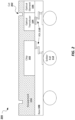
- FIG. 1 is a schematic block diagram of an example optical fiber accommodating chip package 100 in accordance with embodiments of the present disclosure.
- Chip package 100 includes a chip 102 adjacent to and electrically coupled to an optical transducer 104.
- Optical transducer 104 can receive electrical signals from the chip 102 and convert the electrical signals into optical signals.
- the optical transducer 104 can emit the optical signals through the optical element 106.
- Optical element 106 can include any type of fiber optic compatible material (e.g., can transmit optical signals to and from an optical fiber), such as glass, optical-grade polymer, or other material.
- the chip package 100 includes a base 108 upon which the chip 102, the optical transducer 104, and the optical element 106 reside.
- the base 108 can include a dielectric material that can be processed to include a redistribution layer (RDL) 110.
- the RDL 110 can provide electrical interconnectivity between integrated circuit elements, and can facilitate access to integrated circuit elements through contact points, such as solder balls 112, contact pads, or other electrical contacts.
- the chip package 100 also includes an encasement 114.
- Encasement 114 can include a mold compound, such as that used in embedded Wafer Level Ball Grid Array (eWLB) processing or other fan-out WLB processing techniques and flip-chip, or any other process that uses a mold cap.
- eWLB embedded Wafer Level Ball Grid Array
- the mold compound used during formation of the encasement 114 can be a solid molding compound or a liquid molding compound. Examples of a mold compound include an EG-filled epoxy-based material.
- the encasement 114 includes a notch 116.
- the notch 116 can be formed on the top surface of the encasement 114 at a location proximate the optical transducer 104.
- the notch 116 can be formed on the top surface of the encasement 114 above the optical transducer 104 and near the edge of the chip package 100.
- the notch 116 can be formed via mold pressing.
- the notch 116 can have a predetermined shape and size, and can be positioned to facilitate self-alignment of the optical connector component (shown in FIG. 3 ).
- the notch 116 can be formed based on the shape and size of the corresponding optical fiber connector.
- the optical element 106 resides proximate the edge of the chip package 100.
- the optical element 106 held in place by the encasement 114 or sandwiched between the encasement 114 and the base 108.
- a side of the optical element is flush (or substantially flush) with the edge of the chip package 100 and is, according to the invention, flush with the edge of the encasement 114.
- the side of the optical element 106 that is flush with the edge of the chip package 100 is exposed at the edge of the chip package 102 to transmit (i.e., optically transmit) optical signals to and from an optical fiber.
- FIG. 2 is a schematic block diagram of another example optical fiber accommodating chip package 200 in accordance with embodiments of the present disclosure.
- Chip package 200 is similar to that of chip package 100 and includes similar features as shown in FIG. 2 .
- Chip package 200 includes a cut 202 instead of a notch.
- Cut 202 can be formed by a saw or other cutting device. In some embodiments, the cut 202 can traverse along the entire chip package 200. In some embodiments, the cut 202 can be formed without cutting through the entire encasement 114, but rather, can be formed at a discrete location above the optical transducer 104 and/or above the optical element 106, depending on the shape and size of the optical fiber connector.
- the cut 202 can be formed at a top side of the encasement 114 proximate the optical transducer 104.
- the shape of the cut 202 can be predetermined to accommodate the optical fiber connector, shown in FIG. 3 .
- FIG. 3 is a schematic block diagram of an example optical fiber accommodating chip package and an example optical fiber connector in accordance with embodiments of the present disclosure.
- an optical fiber connector 302 is attached to the chip package 300.
- the optical fiber connector 302 is shaped to contact the top of the encasement 114 and the bottom of the chip package 300 (e.g., by contacting the base 108).
- the optical fiber connector 302 can also be physically biased to form a clamp to apply a clamping force on the chip package 300.
- the optical fiber connector 302 can include a fiber guide 306.
- Fiber guide 306 can be configured to receive an optical fiber 310.
- the fiber guide 306 can provide structure support and strain relief for the optical fiber 310.
- the fiber guide 306 can hold the optical fiber 310 in place, and when the optical fiber connector 302 is connected to the chip package 300, the fiber guide 306 can hold the optical fiber 310 in place and in contact with the optical element 106, so that optical signals can be transmitted from the optical fiber 310 to the optical element 106, and optical signals can be transmitted from the optical element 106 to the optical fiber 310.
- a glue 308 can be used to add further structural support to the connection between the optical fiber connector 302 and the chip package 300.
- the glue 308 can be an optically transparent glue.
- the glue 308 can bind the optical fiber connector 302 to the encasement 114 and other parts of the chip package 300 as needed.
- the optical fiber connector 302 includes a connector hook 304.
- Connector hook 304 can fit into a notch / cut 318.
- the notch / cut 318 represents either the notch 116 from FIG. 1 or the cut 202 from FIG. 2 .
- Either the notch or the cut can be used, depending on the design of the connector hook 304.
- no notch or cut is used, and the optical fiber connector 302 can clamp onto the chip package 300.
- the connector hook 304 can be structured to match the notch / cut 318. Or, the notch / cut 318 can be formed to match the shape of the connector hook 304.
- the optical fiber connector 302 When connecting the optical fiber connector 302, the optical fiber connector 302 can slide over the encasement 114, and the connector hook 304 can connect into the notch / cut 318.
- the connection between the connector hook 304 and the notch / cut 318 can create a mechanical stop, preventing the optical fiber connector 302 from moving towards or away from the chip package 300.
- the connection between the notch and the connector hook 304 may also prevent the optical fiber connector 302 from moving side-to-side, relative the chip package.
- the connector hook 304 and the notch / cut 318 also facilitate self-alignment of the optical fiber connector 302 (and the optical fiber 310) with the chip package 300.
- the notch / cut 318 acts as a guide and hard stop for receiving the connector hook 304.
- solder balls 306 are used to add further mechanical fixation between the optical fiber connector 302 and the base 108.
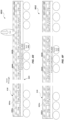
- FIGS. 4A-4F are schematic block diagrams illustrating an example process flow for forming an optical fiber accommodating chip package in accordance with embodiments of the present disclosure.
- the process flow can include an embedded Wafer Level Ball Grid Array (eWI,B) process flow or other type of process flow that can include a separation (e.g., saw separation) and/or a mold pressing process.
- eWI,B embedded Wafer Level Ball Grid Array
- the chips 402a-b, optical transducers 404a-b, and optical elements 406 are placed on a carrier 410 using an adhesive tape 408.
- the chips 402a-b can be a storage or memory chip, processor, or other type of integrated circuit (4002).
- the optical transducers 404a is structured such that each optical element 406 is adjacent to and in optical communication with an optical transducers 404a.
- the optical transducers 404a-b are structured such that each optical element 406 is adjacent to and in optical communication with an optical transducers 404a-b (i.e., one optical transducer 404a on one side of the optical element 406 and one optical transducer 404b on the other side of the optical element 406).
- the arrangement of the chips 402a-b and the optical transducers 404a-b and the optical element 406 can be as follows.
- a chip 402a can reside adjacent to an optical transducer 404a.
- the optical transducer 404a can reside adjacent to the optical element 406, such that the optical transducer 404a is between the chip 402a and the optical element 406.
- the chip 402a and the optical transducer 404a can be electrical coupled through a redistribution layer, discussed later.
- a second optical transducer 404b can reside adjacent to the optical element 406, such that the optical element 406 is between the optical transducer 404a and the optical transducer 404b.
- a chip 402b can reside adjacent to the optical transducer 404b, such that the optical transducer 404b is between the optical element 406 and the chip 402b.
- the chip 402b and the optical transducer 404b can be electrical coupled through a redistribution layer, discussed later.
- a predetermined number of chips, optical transducers, and optical elements can be placed on the carrier 410 in the above described orientation, depending on the size of the carrier.
- an encasement 414 (also referred to as a moldcap 414) is formed (4004).
- the encasement 414 can be formed using a eWLB molding process, or a similar process.
- the encasement 414 covers the chips, optical transducers, and optical elements. In some embodiments, the encasement 414 can hold the chips, optical transducers, and optical elements in place.
- the encasement 414 can be a mold compound, similar to that used in eWLB processing techniques.
- a liquid mold compound can be dispersed over the chips, the optical transducers, and the optical elements and then solidified using known techniques.
- a solid mold compound can be applied using compression molding or other techniques known in the art.
- At least one notch 418 is formed in the encasement 414 (4006).
- Notches 418 can be formed by pressing a toothed structure into the encasement.
- the toothed structure can be part of the mold case used when forming the encasement 414, resulting in a notch in the top of the encasement at predetermined positions.
- the encasement 414 and the chips and optical transducers and optical elements can be removed from the carrier 410 (4008). Also shown in FIG. 4D , the encasement and the chips and optical transducers and optical elements can reside on a base 422 that is fabricated through semiconductor or other dielectric processing techniques.
- the base 422 can be dielectric material that includes a redistribution layer. The redistribution layer can be formed through patterned metal layer deposition or other similar techniques.
- the base 422 can include the redistribution layer shown in FIGS. 1-3 .
- solder balls 420 can be used to physically connect the chips and optical transducers to the base 422. The solder balls can also provide electrical access to various interfaces on the chip and other electronics on the chip package.
- the chip package can undergo singulation to isolate individual chip packages (4010).
- Singulation can be similar to singulation techniques used in eWLB processing.
- the chip package can be sawed through to singulate the chip package.
- the chip package can be sawed through the center of each optical element, e.g., at a location 424. This sawing location can result in the optical element being at an edge of each resulting singulated chip package. Further, the optical element, after singulation, is exposed to the air. Sawing is performed in such a manner that the optical element is cleanly cut. In some embodiments, the optical element can be polished after singulation.
- the chip package can be sawed for singulation through optical elements for all of the optical elements on the original chip package (4012).
- FIGS. 5A-5B are schematic block diagrams illustrating another example process flow for forming an optical fiber accommodating chip package in accordance with embodiments of the present disclosure.
- FIG. 5A starts after the processes shown in FIGS. 4A-B .
- the encasement 414 and the chip and optical transducers and optical elements have been lifted off of the carrier.
- the chip package includes a base and includes solder balls to add physical stability between the chip and optical transducer and the base.
- the chip package undergoes singulation by sawing through the encasement and the base at a location 504 through the optical element (5002).
- the cuts 502 are made in the encasement.
- the cuts 502 will act as the receiver for the optical fiber connector.
- the sawing can result in both the cuts 502 in the encasement and the singulation of the chip package (5004).
- FIGS. 6A-F are schematic diagrams illustrating an example process flow for forming an optical fiber accommodating chip package using flip-chip processing in accordance with embodiments of the present disclosure.
- a set of chips 602a and 602b can be soldered to a prefabricated flip chip substrate that includes a redistribution layer (flip chip substrate + RDL) 612 (6002).
- the resulting structure is illustrated in FIG. 6B (6004).
- the RDL layer can be formed processing the flip chip substrate and designed to accommodate the chip pins and the optical transducer pins.
- the RDL can also provide landing pads for solder balls.
- the optical transducers 604a is structured such that each optical element 406 is adjacent to and in optical communication with an optical transducers 604a.
- the optical transducers 604a-b are structured such that each optical element 606 is adjacent to and in optical communication with an optical transducers 604a-b (i.e., one optical transducer 604a on one side of the optical element 606 and one optical transducer 604b on the other side of the optical element 606).
- the arrangement of the chips 602a-b and the optical transducers 604a-b and the optical element 606 can be as follows.
- a chip 602a can reside adjacent to an optical transducer 604a.
- the optical transducer 604a can reside adjacent to the optical element 606, such that the optical transducer 604a is between the chip 402a and the optical element 606.
- the chip 602a and the optical transducer 604a can be electrical coupled through a redistribution layer, discussed later.
- a second optical transducer 604b can reside adjacent to the optical element 606, such that the optical element 606 is between the optical transducer 604a and the optical transducer 604b.
- a chip 602b can reside adjacent to the optical transducer 604b, such that the optical transducer 604b is between the optical element 606 and the chip 602b.
- the chip 602b and the optical transducer 604b can be electrical coupled through a redistribution layer, discussed later.
- a predetermined number of chips, optical transducers, and optical elements can be placed on the flip chip substrate + RDL 612 in the above described orientation, depending on the size of the substrate.
- an encasement 614 (also referred to as a moldcap 614) is formed (6006).
- the encasement 614 can be formed using a eWLB molding process, or a similar process.
- the encasement 614 covers the chips, optical transducers, and optical elements. In some embodiments, the encasement 614 can hold the chips, optical transducers, and optical elements in place.
- the encasement 614 can be a mold compound, similar to that used in eWLB processing techniques.
- a liquid mold compound can be dispersed over the chips, the optical transducers, and the optical elements and then solidified using known techniques.
- a solid mold compound can be applied using compression molding or other techniques known in the art.
- At least one notch 618 is formed in the encasement 614 (6008).
- Notches 618 can be formed by pressing a toothed structure into the encasement.
- the toothed structure can be part of the mold case used when forming the encasement 614, resulting in a notch in the top of the encasement at predetermined positions.
- solder balls 620 can be used to physically connect the chips and optical transducers to the flip chip substrate + RDL 612. The solder balls can also provide electrical access to various interfaces on the chip and other electronics on the chip package.
- the encasement 614 and the chips and optical transducers and optical elements can be sawed to form singulated packages (6010).
- the chip package can undergo singulation to isolate individual chip packages. Singulation can be similar to singulation techniques used in eWLB processing. For example, the chip package can be sawed through to singulate the chip package.
- the chip package can be sawed through the center of each optical element, e.g., at a location 624. This sawing location can result in the optical element being at an edge of each resulting singulated chip package. Further, the optical element, after singulation, is exposed to the air. Sawing is performed in such a manner that the optical element is cleanly cut. In some embodiments, the optical element can be polished after singulation.
- the chip package can be sawed for singulation through optical elements for all of the optical elements on the original chip package (6012).
- FIGS. 6G-H are schematic diagrams illustrating another example process flow for forming an optical fiber accommodating chip package using flip-chip processing in accordance with embodiments of the present disclosure.
- the chip package undergoes singulation by sawing through the encasement and the flip-chip substrate + RDL 612 at a location 630 through the optical element (6020).
- the cuts 628 are made in the encasement.
- the cuts 628 will act as the receiver for the optical fiber connector. By using the saw to form the cuts 628, the number of tools and steps can be reduced.
- the sawing can result in both the cuts 628 in the encasement and the singulation of the chip package (6022).
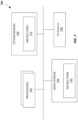
- FIG. 7 is a block diagram of an example computing device 700 that may include or be included in the flexible IC package 100 (e.g., as a wearable IC device).
- the computing device 700 may include one or more processors 702 (e.g., one or more processor cores implemented on one or more components) and a system memory 704 (implemented on one or more components).
- processors 702 e.g., one or more processor cores implemented on one or more components
- system memory 704 implemented on one or more components
- the term "processor” or “processing device” may refer to any device or portion of a device that processes electronic data from registers and/or memory to transform that electronic data into other electronic data that may be stored in registers and/or memory.
- the processor(s) 702 may include one or more microprocessors, graphics processors, digital signal processors, crypto processors, or other suitable devices. More generally, the computing device 700 may include any suitable computational circuitry, such as one or more Application Specific Integrated Circuits (ASICs).
- the computing device 700 may include one or more mass storage devices 706 (such as flash memory devices or any other mass storage device suitable for inclusion in a flexible IC package).
- the system memory 704 and the mass storage device 706 may include any suitable storage devices, such as volatile memory (e.g., dynamic random access memory (DRAM)), nonvolatile memory (e.g., read-only memory (ROM)), and flash memory.
- the computing device 700 may include one or more I/O devices 708 (such as display, user input device, network interface cards, modems, and so forth, suitable for inclusion in a flexible IC device).
- the elements may be coupled to each other via a system bus 712, which represents one or more buses.
- system memory 704 and the mass storage device 706 may be employed to store a working copy and a permanent copy of programming instructions 722.
- the permanent copy of the programming instructions 722 may be placed into permanent mass storage devices 706 in the factory or through a communication device included in the I/O devices 708 (e.g., from a distribution server (not shown)).
- a communication device included in the I/O devices 708 e.g., from a distribution server (not shown)
- the constitution of elements 702-712 are known, and accordingly will not be further described.
- Machine-accessible media including non-transitory computer-readable storage media
- methods, systems, and devices for performing the above-described techniques are illustrative examples of embodiments disclosed herein for thermal management of an IC device.
- a computer-readable media e.g., the system memory 704 and/or the mass storage device 706
- thermal management systems and techniques disclosed herein may be particularly advantageous when used to thermally manage flexible IC packages, these systems and techniques may also be implemented to improve thermal management of conventional, rigid IC packages.
- any of the embodiments disclosed herein and described as applicable in a flexible IC package may also apply in a conventional, rigid IC package setting.
- Such a rigid IC package may include, for example, a rigid substrate material and/or a rigid overmold material.
- thermal management systems and techniques disclosed herein may be particularly advantageous when used to thermally manage components (or “component sections," as discussed above), these systems and techniques may be used to thermally manage any devices included in an IC package, such as a resistor, capacitor, transistor, inductor, radio, memory, processor, laser, light-emitting diode (LED), sensor, a memory gate, combinational or state logic, or other digital or analog component.
- a device thermally managed by the thermal management systems and techniques disclosed herein may be a packaged component (e.g., a surface mount, flip chip, ball grid array, land grid array, bumpless buildup layer, or other package) or an unpackaged component.
Landscapes
- Physics & Mathematics (AREA)
- General Physics & Mathematics (AREA)
- Optics & Photonics (AREA)
- Optical Couplings Of Light Guides (AREA)
Description
- This disclosure pertains to optical fiber connections on package edges, and more particularly, to mechanical and optical connections of optical fibers on package edges.
- Light is getting more and more interesting in the field of data processing. By transferring the data by light, losses (e.g., through wire attenuation) can be reduced. To use light for data transfer, electrical signals are translated into light signals and are inserted into an optical fiber (or fiber optics). On the receiver side, the light is transferred back into electrical signals. On both sides of the optical fiber, the fiber has to be fixed to a chip or package to achieve both mechanical coupling for stability and optical coupling to receive optical signals from the electrical circuitry and emit optical signals to the electrical circuitry.
-
US 2006/0039658 A1 relates to an optoelectronic conversion header, which includes a mounting substrate, a wiring substrate on the mounting substrate, and an integrated circuit on the wiring substrate. The mounting substrate may serve as a heat sink. The optoelectronic conversion header also includes a light emitter and an optical fiber inserted into a ferrule. The light emitter and the ferrule are shown to be located on the mounting substrate. A light absorbing resin covers the entire optoelectronic conversion header. -
US 2011/0182546 A1 relates to a photoelectric conversion device. The device includes an electrical wiring formed on a circuit board. The device includes an optical fiber, and a molded portion covering an end portion and an end face of the optical fiber. The device further includes an optical device optically coupled to the optical fiber through the molded portion. -
US 6293711 B1 discloses an optical transmission module including a substrate having a substantially trapezoidal first groove, an optical device mounted on the substrate for performing conversion between light and electricity, and a ferrule having a center hole and received in the first groove so as to be supported by beveled wall surfaces defining the first groove. An optical fiber is inserted and fixed in the center hole of the ferrule. The ferrule is cut away at a portion opposed to a bottom surface of the first groove. -
US 2005/008302 A1 discloses an optic communications device including an optic communications module which includes a base, an optical element, a fiber optic piece, a ferrule, a transparent resin film, a wiring film, and a sealing member. The base plate and some other elements are divided into individual pieces each making up the optic communications module. -
US 2005 / 141 584 A1 discloses an optical coupler including a semiconductor optical device, a lead frame on which the semiconductor optical device is disposed, a glass submount exemplifying a submount having light transmission and a lens provided on the glass submount. Further, a processing circuit covered with a molding portion is part of the optical coupler. The glass submount is bonded to the lead frame in such a way that the optical portion of the semiconductor optical device which is electrically connected to the glass submount faces an aperture. -
-
FIG. 1 is a schematic diagram of an example optical fiber accommodating chip package in accordance with embodiments of the present disclosure. -
FIG. 2 is a schematic diagram of another example optical fiber accommodating chip package in accordance with embodiments of the present disclosure. -
FIG. 3 is a schematic diagram of an example optical fiber accommodating chip package and an example optical fiber connector in accordance with embodiments of the present disclosure. -
FIGS. 4A-4F are schematic diagrams illustrating an example process flow for forming an optical fiber accommodating chip package in accordance with embodiments of the present disclosure. -
FIGS. 5A-5B are schematic diagrams illustrating another example process flow for forming an optical fiber accommodating chip package in accordance with embodiments of the present disclosure. -
FIGS. 6A-F are schematic diagrams illustrating an example process flow for forming an optical fiber accommodating chip package using flip-chip processing in accordance with embodiments of the present disclosure. -
FIGS. 6G-H are schematic diagrams illustrating another example process flow for forming an optical fiber accommodating chip package using flip-chip processing in accordance with embodiments of the present disclosure. -
FIG. 7 is a schematic block diagram of an example computing device that may be implemented in or include an optical fiber accommodating chip package in accordance with embodiments of the present disclosure. - This disclosure describes a chip package that facilitates a self-aligning optical and mechanical edge connection to an optical fiber. The chip package described herein facilitates the connection of optical fibers directly with the chip package. The chip package described herein allows for shorter connection lengths and reduces the footprint of the system. Additionally, the integration ratio can be increased.
- The chip package formation process can include the following features:
- 1. Implementation of a "optical window component" into the package;
- 2. Creation of a connector-retaining shape by, e.g., mold pressing or sawing; and
- 3. Exposure of an optical element (or window) during the chip package singulation process.
- Other features are readily apparent by the following disclosure, accompanying figures, and the claims.
-
FIG. 1 is a schematic block diagram of an example optical fiber accommodatingchip package 100 in accordance with embodiments of the present disclosure.Chip package 100 includes achip 102 adjacent to and electrically coupled to anoptical transducer 104.Optical transducer 104 can receive electrical signals from thechip 102 and convert the electrical signals into optical signals. Theoptical transducer 104 can emit the optical signals through theoptical element 106.Optical element 106 can include any type of fiber optic compatible material (e.g., can transmit optical signals to and from an optical fiber), such as glass, optical-grade polymer, or other material. Thechip package 100 includes abase 108 upon which thechip 102, theoptical transducer 104, and theoptical element 106 reside. Thebase 108 can include a dielectric material that can be processed to include a redistribution layer (RDL) 110. TheRDL 110 can provide electrical interconnectivity between integrated circuit elements, and can facilitate access to integrated circuit elements through contact points, such assolder balls 112, contact pads, or other electrical contacts. - The
chip package 100 also includes anencasement 114.Encasement 114 can include a mold compound, such as that used in embedded Wafer Level Ball Grid Array (eWLB) processing or other fan-out WLB processing techniques and flip-chip, or any other process that uses a mold cap. (EG filled epoxy-based materials) The mold compound used during formation of theencasement 114 can be a solid molding compound or a liquid molding compound. Examples of a mold compound include an EG-filled epoxy-based material. - The
encasement 114 includes a notch 116. The notch 116 can be formed on the top surface of theencasement 114 at a location proximate theoptical transducer 104. For example, the notch 116 can be formed on the top surface of theencasement 114 above theoptical transducer 104 and near the edge of thechip package 100. The notch 116 can be formed via mold pressing. The notch 116 can have a predetermined shape and size, and can be positioned to facilitate self-alignment of the optical connector component (shown inFIG. 3 ). For example, the notch 116 can be formed based on the shape and size of the corresponding optical fiber connector. - The
optical element 106 resides proximate the edge of thechip package 100. Theoptical element 106 held in place by theencasement 114 or sandwiched between the encasement 114 and thebase 108. A side of the optical element is flush (or substantially flush) with the edge of thechip package 100 and is, according to the invention, flush with the edge of theencasement 114. The side of theoptical element 106 that is flush with the edge of thechip package 100 is exposed at the edge of thechip package 102 to transmit (i.e., optically transmit) optical signals to and from an optical fiber. -
FIG. 2 is a schematic block diagram of another example optical fiber accommodatingchip package 200 in accordance with embodiments of the present disclosure.Chip package 200 is similar to that ofchip package 100 and includes similar features as shown inFIG. 2 .Chip package 200, however, includes acut 202 instead of a notch. Cut 202 can be formed by a saw or other cutting device. In some embodiments, thecut 202 can traverse along theentire chip package 200. In some embodiments, thecut 202 can be formed without cutting through theentire encasement 114, but rather, can be formed at a discrete location above theoptical transducer 104 and/or above theoptical element 106, depending on the shape and size of the optical fiber connector. Thecut 202 can be formed at a top side of theencasement 114 proximate theoptical transducer 104. The shape of thecut 202 can be predetermined to accommodate the optical fiber connector, shown inFIG. 3 . -
FIG. 3 is a schematic block diagram of an example optical fiber accommodating chip package and an example optical fiber connector in accordance with embodiments of the present disclosure. InFIG. 3 , anoptical fiber connector 302 is attached to thechip package 300. Theoptical fiber connector 302 is shaped to contact the top of theencasement 114 and the bottom of the chip package 300 (e.g., by contacting the base 108). Theoptical fiber connector 302 can also be physically biased to form a clamp to apply a clamping force on thechip package 300. - The
optical fiber connector 302 can include afiber guide 306.Fiber guide 306 can be configured to receive anoptical fiber 310. Thefiber guide 306 can provide structure support and strain relief for theoptical fiber 310. Thefiber guide 306 can hold theoptical fiber 310 in place, and when theoptical fiber connector 302 is connected to thechip package 300, thefiber guide 306 can hold theoptical fiber 310 in place and in contact with theoptical element 106, so that optical signals can be transmitted from theoptical fiber 310 to theoptical element 106, and optical signals can be transmitted from theoptical element 106 to theoptical fiber 310. - In some embodiments, a
glue 308 can be used to add further structural support to the connection between theoptical fiber connector 302 and thechip package 300. Theglue 308 can be an optically transparent glue. Theglue 308 can bind theoptical fiber connector 302 to theencasement 114 and other parts of thechip package 300 as needed. - In some embodiments, the
optical fiber connector 302 includes aconnector hook 304.Connector hook 304 can fit into a notch / cut 318. InFIG. 3 , the notch / cut 318 represents either the notch 116 fromFIG. 1 or thecut 202 fromFIG. 2 . Either the notch or the cut can be used, depending on the design of theconnector hook 304. In some embodiments, no notch or cut is used, and theoptical fiber connector 302 can clamp onto thechip package 300. Theconnector hook 304 can be structured to match the notch / cut 318. Or, the notch / cut 318 can be formed to match the shape of theconnector hook 304. - When connecting the
optical fiber connector 302, theoptical fiber connector 302 can slide over theencasement 114, and theconnector hook 304 can connect into the notch / cut 318. The connection between theconnector hook 304 and the notch / cut 318 can create a mechanical stop, preventing theoptical fiber connector 302 from moving towards or away from thechip package 300. When a notch is used, the connection between the notch and theconnector hook 304 may also prevent theoptical fiber connector 302 from moving side-to-side, relative the chip package. - The
connector hook 304 and the notch / cut 318 also facilitate self-alignment of the optical fiber connector 302 (and the optical fiber 310) with thechip package 300. By creating the notch / cut 318 in a predetermined position proximate theoptical transducer 104 and/or theoptical element 106, the notch / cut 318 acts as a guide and hard stop for receiving theconnector hook 304. - In some embodiments,
solder balls 306 are used to add further mechanical fixation between theoptical fiber connector 302 and thebase 108. -
FIGS. 4A-4F are schematic block diagrams illustrating an example process flow for forming an optical fiber accommodating chip package in accordance with embodiments of the present disclosure. In general, the process flow can include an embedded Wafer Level Ball Grid Array (eWI,B) process flow or other type of process flow that can include a separation (e.g., saw separation) and/or a mold pressing process. - As illustrated in
FIG. 4A , thechips 402a-b,optical transducers 404a-b, andoptical elements 406 are placed on acarrier 410 using anadhesive tape 408. Thechips 402a-b can be a storage or memory chip, processor, or other type of integrated circuit (4002). - In some embodiments, the
optical transducers 404a is structured such that eachoptical element 406 is adjacent to and in optical communication with anoptical transducers 404a. In some embodiments, theoptical transducers 404a-b are structured such that eachoptical element 406 is adjacent to and in optical communication with anoptical transducers 404a-b (i.e., oneoptical transducer 404a on one side of theoptical element 406 and oneoptical transducer 404b on the other side of the optical element 406). - The arrangement of the
chips 402a-b and theoptical transducers 404a-b and theoptical element 406 can be as follows. Achip 402a can reside adjacent to anoptical transducer 404a. Theoptical transducer 404a can reside adjacent to theoptical element 406, such that theoptical transducer 404a is between thechip 402a and theoptical element 406. Thechip 402a and theoptical transducer 404a can be electrical coupled through a redistribution layer, discussed later. A secondoptical transducer 404b can reside adjacent to theoptical element 406, such that theoptical element 406 is between theoptical transducer 404a and theoptical transducer 404b. Achip 402b can reside adjacent to theoptical transducer 404b, such that theoptical transducer 404b is between theoptical element 406 and thechip 402b. Thechip 402b and theoptical transducer 404b can be electrical coupled through a redistribution layer, discussed later. - A predetermined number of chips, optical transducers, and optical elements can be placed on the
carrier 410 in the above described orientation, depending on the size of the carrier. - As illustrated in
FIG. 4B , an encasement 414 (also referred to as a moldcap 414) is formed (4004). Theencasement 414 can be formed using a eWLB molding process, or a similar process. Theencasement 414 covers the chips, optical transducers, and optical elements. In some embodiments, theencasement 414 can hold the chips, optical transducers, and optical elements in place. Theencasement 414 can be a mold compound, similar to that used in eWLB processing techniques. A liquid mold compound can be dispersed over the chips, the optical transducers, and the optical elements and then solidified using known techniques. A solid mold compound can be applied using compression molding or other techniques known in the art. - As illustrated in
FIG. 4C , at least one notch 418 is formed in the encasement 414 (4006). Notches 418 can be formed by pressing a toothed structure into the encasement. The toothed structure can be part of the mold case used when forming theencasement 414, resulting in a notch in the top of the encasement at predetermined positions. - As illustrated in
FIG. 4D , theencasement 414 and the chips and optical transducers and optical elements can be removed from the carrier 410 (4008). Also shown inFIG. 4D , the encasement and the chips and optical transducers and optical elements can reside on a base 422 that is fabricated through semiconductor or other dielectric processing techniques. The base 422 can be dielectric material that includes a redistribution layer. The redistribution layer can be formed through patterned metal layer deposition or other similar techniques. The base 422 can include the redistribution layer shown inFIGS. 1-3 . In some embodiments,solder balls 420 can be used to physically connect the chips and optical transducers to thebase 422. The solder balls can also provide electrical access to various interfaces on the chip and other electronics on the chip package. - As illustrated in
FIG. 4E , the chip package can undergo singulation to isolate individual chip packages (4010). Singulation can be similar to singulation techniques used in eWLB processing. For example, the chip package can be sawed through to singulate the chip package. - The chip package can be sawed through the center of each optical element, e.g., at a
location 424. This sawing location can result in the optical element being at an edge of each resulting singulated chip package. Further, the optical element, after singulation, is exposed to the air. Sawing is performed in such a manner that the optical element is cleanly cut. In some embodiments, the optical element can be polished after singulation. - As illustrated in
FIG. 4F , the chip package can be sawed for singulation through optical elements for all of the optical elements on the original chip package (4012). -
FIGS. 5A-5B are schematic block diagrams illustrating another example process flow for forming an optical fiber accommodating chip package in accordance with embodiments of the present disclosure.FIG. 5A starts after the processes shown inFIGS. 4A-B . As illustrated inFIG. 5A , theencasement 414 and the chip and optical transducers and optical elements have been lifted off of the carrier. InFIG. 5A , the chip package includes a base and includes solder balls to add physical stability between the chip and optical transducer and the base. - As illustrated in
FIG. 5A , the chip package undergoes singulation by sawing through the encasement and the base at alocation 504 through the optical element (5002). In the same sawing process, thecuts 502 are made in the encasement. Thecuts 502 will act as the receiver for the optical fiber connector. By using the saw to form thecuts 502, the number of tools and steps can be reduced. - As illustrated in
FIG. 5B , the sawing can result in both thecuts 502 in the encasement and the singulation of the chip package (5004). -
FIGS. 6A-F are schematic diagrams illustrating an example process flow for forming an optical fiber accommodating chip package using flip-chip processing in accordance with embodiments of the present disclosure. - As illustrated in
FIG. 6A , a set ofchips FIG. 6B (6004). The RDL layer can be formed processing the flip chip substrate and designed to accommodate the chip pins and the optical transducer pins. The RDL can also provide landing pads for solder balls. - In some embodiments, the
optical transducers 604a is structured such that eachoptical element 406 is adjacent to and in optical communication with anoptical transducers 604a. In some embodiments, theoptical transducers 604a-b are structured such that eachoptical element 606 is adjacent to and in optical communication with anoptical transducers 604a-b (i.e., oneoptical transducer 604a on one side of theoptical element 606 and oneoptical transducer 604b on the other side of the optical element 606). - The arrangement of the
chips 602a-b and theoptical transducers 604a-b and theoptical element 606 can be as follows. Achip 602a can reside adjacent to anoptical transducer 604a. Theoptical transducer 604a can reside adjacent to theoptical element 606, such that theoptical transducer 604a is between thechip 402a and theoptical element 606. Thechip 602a and theoptical transducer 604a can be electrical coupled through a redistribution layer, discussed later. A secondoptical transducer 604b can reside adjacent to theoptical element 606, such that theoptical element 606 is between theoptical transducer 604a and theoptical transducer 604b. Achip 602b can reside adjacent to theoptical transducer 604b, such that theoptical transducer 604b is between theoptical element 606 and thechip 602b. Thechip 602b and theoptical transducer 604b can be electrical coupled through a redistribution layer, discussed later. - A predetermined number of chips, optical transducers, and optical elements can be placed on the flip chip substrate +
RDL 612 in the above described orientation, depending on the size of the substrate. - As illustrated in
FIG. 6C , an encasement 614 (also referred to as a moldcap 614) is formed (6006). Theencasement 614 can be formed using a eWLB molding process, or a similar process. Theencasement 614 covers the chips, optical transducers, and optical elements. In some embodiments, theencasement 614 can hold the chips, optical transducers, and optical elements in place. Theencasement 614 can be a mold compound, similar to that used in eWLB processing techniques. A liquid mold compound can be dispersed over the chips, the optical transducers, and the optical elements and then solidified using known techniques. A solid mold compound can be applied using compression molding or other techniques known in the art. - As illustrated in
FIG. 6D , at least onenotch 618 is formed in the encasement 614 (6008).Notches 618 can be formed by pressing a toothed structure into the encasement. The toothed structure can be part of the mold case used when forming theencasement 614, resulting in a notch in the top of the encasement at predetermined positions. In some embodiments,solder balls 620 can be used to physically connect the chips and optical transducers to the flip chip substrate +RDL 612. The solder balls can also provide electrical access to various interfaces on the chip and other electronics on the chip package. - As illustrated in
FIG. 6E , theencasement 614 and the chips and optical transducers and optical elements can be sawed to form singulated packages (6010). The chip package can undergo singulation to isolate individual chip packages. Singulation can be similar to singulation techniques used in eWLB processing. For example, the chip package can be sawed through to singulate the chip package. - The chip package can be sawed through the center of each optical element, e.g., at a
location 624. This sawing location can result in the optical element being at an edge of each resulting singulated chip package. Further, the optical element, after singulation, is exposed to the air. Sawing is performed in such a manner that the optical element is cleanly cut. In some embodiments, the optical element can be polished after singulation. - As illustrated in
FIG. 6F , the chip package can be sawed for singulation through optical elements for all of the optical elements on the original chip package (6012). -
FIGS. 6G-H are schematic diagrams illustrating another example process flow for forming an optical fiber accommodating chip package using flip-chip processing in accordance with embodiments of the present disclosure. As illustrated inFIG. 6G , the chip package undergoes singulation by sawing through the encasement and the flip-chip substrate +RDL 612 at alocation 630 through the optical element (6020). In the same sawing process, thecuts 628 are made in the encasement. Thecuts 628 will act as the receiver for the optical fiber connector. By using the saw to form thecuts 628, the number of tools and steps can be reduced. - As illustrated in
FIG. 6H , the sawing can result in both thecuts 628 in the encasement and the singulation of the chip package (6022). -
FIG. 7 is a block diagram of anexample computing device 700 that may include or be included in the flexible IC package 100 (e.g., as a wearable IC device). As shown, thecomputing device 700 may include one or more processors 702 (e.g., one or more processor cores implemented on one or more components) and a system memory 704 (implemented on one or more components). As used herein, the term "processor" or "processing device" may refer to any device or portion of a device that processes electronic data from registers and/or memory to transform that electronic data into other electronic data that may be stored in registers and/or memory. The processor(s) 702 may include one or more microprocessors, graphics processors, digital signal processors, crypto processors, or other suitable devices. More generally, thecomputing device 700 may include any suitable computational circuitry, such as one or more Application Specific Integrated Circuits (ASICs). - The
computing device 700 may include one or more mass storage devices 706 (such as flash memory devices or any other mass storage device suitable for inclusion in a flexible IC package). Thesystem memory 704 and themass storage device 706 may include any suitable storage devices, such as volatile memory (e.g., dynamic random access memory (DRAM)), nonvolatile memory (e.g., read-only memory (ROM)), and flash memory. Thecomputing device 700 may include one or more I/O devices 708 (such as display, user input device, network interface cards, modems, and so forth, suitable for inclusion in a flexible IC device). The elements may be coupled to each other via a system bus 712, which represents one or more buses. - Each of these elements may perform its conventional functions known in the art. In particular, the
system memory 704 and themass storage device 706 may be employed to store a working copy and a permanent copy ofprogramming instructions 722. - The permanent copy of the
programming instructions 722 may be placed into permanentmass storage devices 706 in the factory or through a communication device included in the I/O devices 708 (e.g., from a distribution server (not shown)). The constitution of elements 702-712 are known, and accordingly will not be further described. - Machine-accessible media (including non-transitory computer-readable storage media), methods, systems, and devices for performing the above-described techniques are illustrative examples of embodiments disclosed herein for thermal management of an IC device. For example, a computer-readable media (e.g., the
system memory 704 and/or the mass storage device 706) may have stored thereon instructions (e.g., the instructions 722) such that, when the instructions are executed by one or more of theprocessors 702. - As noted above, although the thermal management systems and techniques disclosed herein may be particularly advantageous when used to thermally manage flexible IC packages, these systems and techniques may also be implemented to improve thermal management of conventional, rigid IC packages. Thus, any of the embodiments disclosed herein and described as applicable in a flexible IC package may also apply in a conventional, rigid IC package setting. Such a rigid IC package may include, for example, a rigid substrate material and/or a rigid overmold material.
- Additionally, although the thermal management systems and techniques disclosed herein may be particularly advantageous when used to thermally manage components (or "component sections," as discussed above), these systems and techniques may be used to thermally manage any devices included in an IC package, such as a resistor, capacitor, transistor, inductor, radio, memory, processor, laser, light-emitting diode (LED), sensor, a memory gate, combinational or state logic, or other digital or analog component. A device thermally managed by the thermal management systems and techniques disclosed herein may be a packaged component (e.g., a surface mount, flip chip, ball grid array, land grid array, bumpless buildup layer, or other package) or an unpackaged component.
- The relative sizes of features shown in the figures are not drawn to scale.
Claims (11)
- A method comprising:providing (4002) an optical transducer (104, 404) and an optical element (106, 406) adjacent to the optical transducer (104, 404) on a carrier (410);encasing (4004) the optical transducer (104, 404) and the optical element (106, 406) with an encasement (114, 414);forming (4010) a connector receiver (116, 202, 418, 502) in the encasement (114, 414) at a top side of the encasement (114, 414) at a location proximate to the optical transducer (104, 404), wherein the connector receiver (116, 202, 418, 502) is for receiving a tooth (304) of an optical fiber connector (302); andcutting (4010) the encasement (114, 414) and the optical element (106, 406) to expose a side of the optical element (106, 406), wherein the side of the optical element (106, 406) is flush with the edge of the encasement (114, 414).
- The method of claim 1, further comprising providing (4002) an integrated circuit (102) proximate the optical transducer (104, 404), the optical transducer (104, 404) between the optical element (106, 406) and the integrated circuit (102).
- The method of claim 1 or 2, wherein the optical transducer (104, 404) is a first optical transducer (404a), and wherein the first optical transducer (404a) resides on a first side of the optical element (106, 406), the method further comprising:providing a second optical transducer (404b) residing on a second side of the optical element (106, 406), opposite the first side of the optical element (106, 406); andwherein cutting the encasement (114, 414) and the optical element (106, 406) comprises:
cutting through the optical element (106, 406) to divide the optical element (106, 406) into two segments, a first segment of the optical element (106, 406) adjacent to the first optical transducer (404a) and a second segment of the optical element adjacent to the second optical transducer (404b). - The method of any of claims 1 or 3, further a comprising forming (4008) a base (108, 422) on an exposed side of the optical transducer (104, 404) and forming a redistribution layer (110) in the base (108, 422).
- The method of claim 1 or 3 or 4, further comprising forming (4008) one or more solder balls (112, 420) electrically connected to the optical transducer (104, 404) through a redistribution layer (110) in the base (108, 422).
- The method of claim 1, wherein providing an optical transducer (104, 404) and an optical element (106, 406) adjacent to the optical transducer (104, 404) on a carrier (410) comprises soldering the optical transducer (104, 404) to a prefabricated substrate, the prefabricated substrate comprising an integrated redistribution layer (RDL) (110), wherein soldering the optical transducer (104, 404) to the prefabricated substrate comprises soldering the optical transducer (104, 404) to a contact pad of the RDL (110).
- An apparatus (100, 300) comprising:a base (108, 422) comprising a redistribution layer (110) for providing electrical interconnectivity;an optical transducer circuit element (104, 404) on the base electrically connected to the redistribution layer (110);an optical element (106, 406) adjacent to the optical transducer circuit element (104, 404) and at an edge of the base (108, 422), wherein the optical transducer circuit element (104, 404) is configured to convert electrical signals into optical signals, and to emit the optical signals through the optical element (106, 406);an encasement (114, 414) encasing the optical transducer circuit element (104, 404) and a portion of the optical element (106, 406), wherein one side of the optical element (106, 406) is exposed at an edge of the encasement (114, 414) and at the edge of the base (108, 422), wherein the side of the optical element (106, 406) is flush with the edge of the encasement (114, 414), wherein a bottom side of the encasement (114, 414) is facing the base (108, 422);a connector receiver (116, 202, 418, 502) formed on a top side opposite the bottom side of the encasement (114, 414) at a location in the encasement proximate the optical transducer (104, 404), wherein the connector receiver (116, 202, 418, 502) is for receiving a tooth (304) of an optical fiber connector (302).
- The apparatus of claim 7, further comprising an integrated circuit (102) residing on the base (108, 422) and electrically connected to the redistribution layer (110), the optical transducer circuit element (104, 404) residing between the optical element (106, 406) and the integrated circuit (102).
- A computing system (700) comprising the apparatus of claim 8, and further comprising an optical fiber connector (302) connected to the edge of the encasement (114, 414), the optical fiber connector (302) comprising a clamp and a tooth (304) on an inner portion of the clamp, the tooth (304) received in the connector receiver (116, 202, 418, 502).
- The computing system of claim 9, wherein the optical fiber connector (302) comprises an optical fiber (310) in contact with the exposed portion of the optical element (106, 406), the optical fiber connector (302) securing the optical fiber in place (310).
- The computing system of claim 9 or 10, further comprising a transparent glue (308) securing the optical fiber connector (302) against the edge of the encasement (114, 414).
Applications Claiming Priority (1)
| Application Number | Priority Date | Filing Date | Title |
|---|---|---|---|
| PCT/US2016/024400 WO2017171696A1 (en) | 2016-03-28 | 2016-03-28 | Optical fiber connection on package edge |
Publications (3)
| Publication Number | Publication Date |
|---|---|
| EP3436857A1 EP3436857A1 (en) | 2019-02-06 |
| EP3436857A4 EP3436857A4 (en) | 2019-10-02 |
| EP3436857B1 true EP3436857B1 (en) | 2024-12-25 |
Family
ID=59964992
Family Applications (1)
| Application Number | Title | Priority Date | Filing Date |
|---|---|---|---|
| EP16897257.8A Active EP3436857B1 (en) | 2016-03-28 | 2016-03-28 | Optical fiber connection on package edge |
Country Status (3)
| Country | Link |
|---|---|
| US (1) | US20190121041A1 (en) |
| EP (1) | EP3436857B1 (en) |
| WO (1) | WO2017171696A1 (en) |
Families Citing this family (7)
| Publication number | Priority date | Publication date | Assignee | Title |
|---|---|---|---|---|
| US10777430B2 (en) | 2018-06-27 | 2020-09-15 | Taiwan Semiconductor Manufacturing Company, Ltd. | Photonic integrated package and method forming same |
| US11493713B1 (en) * | 2018-09-19 | 2022-11-08 | Psiquantum, Corp. | Photonic quantum computer assembly having dies with specific contact configuration and matched CTE |
| US11315878B2 (en) * | 2018-10-31 | 2022-04-26 | Taiwan Semiconductor Manufacturing Company, Ltd. | Photonics integrated circuit package |
| WO2022041159A1 (en) * | 2020-08-28 | 2022-03-03 | 华为技术有限公司 | Chip packaging structure, electronic device, and method for preparing chip packaging structure |
| US11762155B2 (en) * | 2021-08-25 | 2023-09-19 | Cisco Technology, Inc. | Photonics packaging platform |
| EP4421852A4 (en) * | 2021-11-22 | 2024-12-11 | Huawei Technologies Co., Ltd. | PHOTOELECTRIC TRANSMITTER-RECEIVE ARRANGEMENT AND METHOD FOR THE PRODUCTION THEREOF |
| US20230200119A1 (en) * | 2021-12-20 | 2023-06-22 | Intel Corporation | Organic thin-films for data transmission |
Citations (2)
| Publication number | Priority date | Publication date | Assignee | Title |
|---|---|---|---|---|
| US20050008302A1 (en) * | 2003-06-18 | 2005-01-13 | Seiko Epson Corporation | Optic communications module, method for manufacturing the same, optic communications device, and electronic equipment |
| US20050141584A1 (en) * | 2003-12-24 | 2005-06-30 | Sharp Kabushiki Kaisha | Optical coupler and electronic equipment using same |
Family Cites Families (9)
| Publication number | Priority date | Publication date | Assignee | Title |
|---|---|---|---|---|
| JPH11264920A (en) * | 1998-03-18 | 1999-09-28 | Fujitsu Ltd | Optical transmission module |
| JP3989316B2 (en) * | 2002-07-15 | 2007-10-10 | 株式会社巴川製紙所 | Optical fiber connection method and optical fiber connection structure |
| DE10332015A1 (en) * | 2003-07-14 | 2005-03-03 | Infineon Technologies Ag | Optoelectronic module with transmitter chip and connector for the module to an optical fiber and to a circuit board, and method of making the same |
| US7352935B2 (en) | 2004-08-17 | 2008-04-01 | Kabushiki Kaisha Toshiba | Optoelectronic conversion header, LSI package with interface module, method of manufacturing optoelectronic conversion header, and optical interconnection system |
| JP4676975B2 (en) * | 2007-09-13 | 2011-04-27 | シャープ株式会社 | Bi-directional optical transmission device |
| JP5212390B2 (en) * | 2010-01-26 | 2013-06-19 | 日立電線株式会社 | Photoelectric conversion device |
| US8871570B2 (en) * | 2012-03-14 | 2014-10-28 | Mellanox Technologies Ltd. | Method of fabricating integrated optoelectronic interconnects with side mounted transducer |
| US8961039B2 (en) * | 2012-06-21 | 2015-02-24 | Hirose Electric Co., Ltd. | Optical-electric conversion connector |
| US11133870B2 (en) * | 2013-08-13 | 2021-09-28 | Commscope, Inc. Of North Carolina | Fiber optic connectors and connectorized fiber optic cables that include integrated photonic optical mode field converters and related methods |
-
2016
- 2016-03-28 WO PCT/US2016/024400 patent/WO2017171696A1/en not_active Ceased
- 2016-03-28 US US16/090,024 patent/US20190121041A1/en not_active Abandoned
- 2016-03-28 EP EP16897257.8A patent/EP3436857B1/en active Active
Patent Citations (2)
| Publication number | Priority date | Publication date | Assignee | Title |
|---|---|---|---|---|
| US20050008302A1 (en) * | 2003-06-18 | 2005-01-13 | Seiko Epson Corporation | Optic communications module, method for manufacturing the same, optic communications device, and electronic equipment |
| US20050141584A1 (en) * | 2003-12-24 | 2005-06-30 | Sharp Kabushiki Kaisha | Optical coupler and electronic equipment using same |
Also Published As
| Publication number | Publication date |
|---|---|
| EP3436857A4 (en) | 2019-10-02 |
| US20190121041A1 (en) | 2019-04-25 |
| WO2017171696A1 (en) | 2017-10-05 |
| EP3436857A1 (en) | 2019-02-06 |
Similar Documents
| Publication | Publication Date | Title |
|---|---|---|
| US20190121041A1 (en) | Optical fiber connection on package edge | |
| US10866373B2 (en) | Optical transceiver and manufacturing method thereof | |
| US10598860B2 (en) | Photonic die fan out package with edge fiber coupling interface and related methods | |
| CN107134438B (en) | Semiconductor device and method of forming an insulating layer around a semiconductor die | |
| US11205636B2 (en) | Semiconductor package and method of manufacturing the same | |
| EP0618468B1 (en) | An interface for coupling optical fibers to electronic circuitry | |
| US8290008B2 (en) | Silicon carrier optoelectronic packaging | |
| CN112103275B (en) | Packaging method of silicon optical module and silicon optical module | |
| US6982491B1 (en) | Sensor semiconductor package and method of manufacturing the same | |
| JP7642659B2 (en) | Chip-Last Wafer-Level Fan-Out with Optical Fiber Alignment Structure | |
| CN202351465U (en) | Optical element and electronic package with optical element | |
| US20250291139A1 (en) | Package assembly and manufacturing method thereof | |
| US8842951B2 (en) | Systems and methods for passive alignment of opto-electronic components | |
| CN107068663B (en) | Semiconductor chip package with optical interface | |
| US20100151614A1 (en) | Wafer level method of forming side fiber insertion optoelectronic packages | |
| EP0561964A1 (en) | Optoelectronic device component package and method of making the same | |
| US5587605A (en) | Package for mating with a semiconductor die | |
| US20220271019A1 (en) | Semiconductor package structure and method of manufacturing the same | |
| US11508766B2 (en) | Molded image sensor chip scale packages and related methods | |
| CN109524382B (en) | Chip packaging structure and packaging method | |
| US9551846B1 (en) | Method for manufacturing optical engine packages and apparatus from which optical engine packages are manufactured | |
| CN120166808A (en) | Optical sensor packaging | |
| US20070065958A1 (en) | Method for attaching an optical filter to an encapsulated package |
Legal Events
| Date | Code | Title | Description |
|---|---|---|---|
| STAA | Information on the status of an ep patent application or granted ep patent |
Free format text: STATUS: THE INTERNATIONAL PUBLICATION HAS BEEN MADE |
|
| PUAI | Public reference made under article 153(3) epc to a published international application that has entered the european phase |
Free format text: ORIGINAL CODE: 0009012 |
|
| STAA | Information on the status of an ep patent application or granted ep patent |
Free format text: STATUS: REQUEST FOR EXAMINATION WAS MADE |
|
| 17P | Request for examination filed |
Effective date: 20180828 |
|
| AK | Designated contracting states |
Kind code of ref document: A1 Designated state(s): AL AT BE BG CH CY CZ DE DK EE ES FI FR GB GR HR HU IE IS IT LI LT LU LV MC MK MT NL NO PL PT RO RS SE SI SK SM TR |
|
| AX | Request for extension of the european patent |
Extension state: BA ME |
|
| DAV | Request for validation of the european patent (deleted) | ||
| DAX | Request for extension of the european patent (deleted) | ||
| A4 | Supplementary search report drawn up and despatched |
Effective date: 20190904 |
|
| RIC1 | Information provided on ipc code assigned before grant |
Ipc: G02B 6/42 20060101AFI20190829BHEP |
|
| STAA | Information on the status of an ep patent application or granted ep patent |
Free format text: STATUS: THE APPLICATION HAS BEEN WITHDRAWN |
|
| STAA | Information on the status of an ep patent application or granted ep patent |
Free format text: STATUS: REQUEST FOR EXAMINATION WAS MADE |
|
| 18W | Application withdrawn |
Effective date: 20210209 |
|
| D18W | Application withdrawn (deleted) | ||
| STAA | Information on the status of an ep patent application or granted ep patent |
Free format text: STATUS: EXAMINATION IS IN PROGRESS |
|
| 17Q | First examination report despatched |
Effective date: 20210607 |
|
| RAP1 | Party data changed (applicant data changed or rights of an application transferred) |
Owner name: INTEL IP CORPORATION |
|
| RAP1 | Party data changed (applicant data changed or rights of an application transferred) |
Owner name: INTEL CORPORATION |
|
| GRAP | Despatch of communication of intention to grant a patent |
Free format text: ORIGINAL CODE: EPIDOSNIGR1 |
|
| STAA | Information on the status of an ep patent application or granted ep patent |
Free format text: STATUS: GRANT OF PATENT IS INTENDED |
|
| INTG | Intention to grant announced |
Effective date: 20240722 |
|
| GRAS | Grant fee paid |
Free format text: ORIGINAL CODE: EPIDOSNIGR3 |
|
| GRAA | (expected) grant |
Free format text: ORIGINAL CODE: 0009210 |
|
| STAA | Information on the status of an ep patent application or granted ep patent |
Free format text: STATUS: THE PATENT HAS BEEN GRANTED |
|
| AK | Designated contracting states |
Kind code of ref document: B1 Designated state(s): AL AT BE BG CH CY CZ DE DK EE ES FI FR GB GR HR HU IE IS IT LI LT LU LV MC MK MT NL NO PL PT RO RS SE SI SK SM TR |
|
| REG | Reference to a national code |
Ref country code: CH Ref legal event code: EP |
|
| REG | Reference to a national code |
Ref country code: DE Ref legal event code: R096 Ref document number: 602016090762 Country of ref document: DE |
|
| REG | Reference to a national code |
Ref country code: IE Ref legal event code: FG4D |
|
| P01 | Opt-out of the competence of the unified patent court (upc) registered |
Free format text: CASE NUMBER: APP_68035/2024 Effective date: 20241225 |
|
| REG | Reference to a national code |
Ref country code: NL Ref legal event code: FP |
|
| REG | Reference to a national code |
Ref country code: LT Ref legal event code: MG9D |
|
| PG25 | Lapsed in a contracting state [announced via postgrant information from national office to epo] |
Ref country code: HR Free format text: LAPSE BECAUSE OF FAILURE TO SUBMIT A TRANSLATION OF THE DESCRIPTION OR TO PAY THE FEE WITHIN THE PRESCRIBED TIME-LIMIT Effective date: 20241225 |
|
| PG25 | Lapsed in a contracting state [announced via postgrant information from national office to epo] |
Ref country code: FI Free format text: LAPSE BECAUSE OF FAILURE TO SUBMIT A TRANSLATION OF THE DESCRIPTION OR TO PAY THE FEE WITHIN THE PRESCRIBED TIME-LIMIT Effective date: 20241225 |
|
| PG25 | Lapsed in a contracting state [announced via postgrant information from national office to epo] |
Ref country code: BG Free format text: LAPSE BECAUSE OF FAILURE TO SUBMIT A TRANSLATION OF THE DESCRIPTION OR TO PAY THE FEE WITHIN THE PRESCRIBED TIME-LIMIT Effective date: 20241225 |
|
| PG25 | Lapsed in a contracting state [announced via postgrant information from national office to epo] |
Ref country code: NO Free format text: LAPSE BECAUSE OF FAILURE TO SUBMIT A TRANSLATION OF THE DESCRIPTION OR TO PAY THE FEE WITHIN THE PRESCRIBED TIME-LIMIT Effective date: 20250325 |
|
| PG25 | Lapsed in a contracting state [announced via postgrant information from national office to epo] |
Ref country code: GR Free format text: LAPSE BECAUSE OF FAILURE TO SUBMIT A TRANSLATION OF THE DESCRIPTION OR TO PAY THE FEE WITHIN THE PRESCRIBED TIME-LIMIT Effective date: 20250326 Ref country code: LV Free format text: LAPSE BECAUSE OF FAILURE TO SUBMIT A TRANSLATION OF THE DESCRIPTION OR TO PAY THE FEE WITHIN THE PRESCRIBED TIME-LIMIT Effective date: 20241225 |
|
| PG25 | Lapsed in a contracting state [announced via postgrant information from national office to epo] |
Ref country code: RS Free format text: LAPSE BECAUSE OF FAILURE TO SUBMIT A TRANSLATION OF THE DESCRIPTION OR TO PAY THE FEE WITHIN THE PRESCRIBED TIME-LIMIT Effective date: 20250325 |
|
| REG | Reference to a national code |
Ref country code: AT Ref legal event code: MK05 Ref document number: 1754644 Country of ref document: AT Kind code of ref document: T Effective date: 20241225 |
|
| PG25 | Lapsed in a contracting state [announced via postgrant information from national office to epo] |
Ref country code: SM Free format text: LAPSE BECAUSE OF FAILURE TO SUBMIT A TRANSLATION OF THE DESCRIPTION OR TO PAY THE FEE WITHIN THE PRESCRIBED TIME-LIMIT Effective date: 20241225 |
|
| PG25 | Lapsed in a contracting state [announced via postgrant information from national office to epo] |
Ref country code: PL Free format text: LAPSE BECAUSE OF FAILURE TO SUBMIT A TRANSLATION OF THE DESCRIPTION OR TO PAY THE FEE WITHIN THE PRESCRIBED TIME-LIMIT Effective date: 20241225 |
|
| PG25 | Lapsed in a contracting state [announced via postgrant information from national office to epo] |
Ref country code: ES Free format text: LAPSE BECAUSE OF FAILURE TO SUBMIT A TRANSLATION OF THE DESCRIPTION OR TO PAY THE FEE WITHIN THE PRESCRIBED TIME-LIMIT Effective date: 20241225 |
|
| PG25 | Lapsed in a contracting state [announced via postgrant information from national office to epo] |
Ref country code: IS Free format text: LAPSE BECAUSE OF FAILURE TO SUBMIT A TRANSLATION OF THE DESCRIPTION OR TO PAY THE FEE WITHIN THE PRESCRIBED TIME-LIMIT Effective date: 20250425 |
|
| PG25 | Lapsed in a contracting state [announced via postgrant information from national office to epo] |
Ref country code: PT Free format text: LAPSE BECAUSE OF FAILURE TO SUBMIT A TRANSLATION OF THE DESCRIPTION OR TO PAY THE FEE WITHIN THE PRESCRIBED TIME-LIMIT Effective date: 20250428 |
|
| PG25 | Lapsed in a contracting state [announced via postgrant information from national office to epo] |
Ref country code: EE Free format text: LAPSE BECAUSE OF FAILURE TO SUBMIT A TRANSLATION OF THE DESCRIPTION OR TO PAY THE FEE WITHIN THE PRESCRIBED TIME-LIMIT Effective date: 20241225 |
|
| PG25 | Lapsed in a contracting state [announced via postgrant information from national office to epo] |
Ref country code: AT Free format text: LAPSE BECAUSE OF FAILURE TO SUBMIT A TRANSLATION OF THE DESCRIPTION OR TO PAY THE FEE WITHIN THE PRESCRIBED TIME-LIMIT Effective date: 20241225 |
|
| PG25 | Lapsed in a contracting state [announced via postgrant information from national office to epo] |
Ref country code: SK Free format text: LAPSE BECAUSE OF FAILURE TO SUBMIT A TRANSLATION OF THE DESCRIPTION OR TO PAY THE FEE WITHIN THE PRESCRIBED TIME-LIMIT Effective date: 20241225 |
|
| PG25 | Lapsed in a contracting state [announced via postgrant information from national office to epo] |
Ref country code: CZ Free format text: LAPSE BECAUSE OF FAILURE TO SUBMIT A TRANSLATION OF THE DESCRIPTION OR TO PAY THE FEE WITHIN THE PRESCRIBED TIME-LIMIT Effective date: 20241225 |
|
| PG25 | Lapsed in a contracting state [announced via postgrant information from national office to epo] |
Ref country code: IT Free format text: LAPSE BECAUSE OF FAILURE TO SUBMIT A TRANSLATION OF THE DESCRIPTION OR TO PAY THE FEE WITHIN THE PRESCRIBED TIME-LIMIT Effective date: 20241225 |
|
| PG25 | Lapsed in a contracting state [announced via postgrant information from national office to epo] |
Ref country code: SE Free format text: LAPSE BECAUSE OF FAILURE TO SUBMIT A TRANSLATION OF THE DESCRIPTION OR TO PAY THE FEE WITHIN THE PRESCRIBED TIME-LIMIT Effective date: 20241225 |
|
| REG | Reference to a national code |
Ref country code: DE Ref legal event code: R097 Ref document number: 602016090762 Country of ref document: DE |
|
| PG25 | Lapsed in a contracting state [announced via postgrant information from national office to epo] |
Ref country code: DK Free format text: LAPSE BECAUSE OF FAILURE TO SUBMIT A TRANSLATION OF THE DESCRIPTION OR TO PAY THE FEE WITHIN THE PRESCRIBED TIME-LIMIT Effective date: 20241225 |
|
| PG25 | Lapsed in a contracting state [announced via postgrant information from national office to epo] |
Ref country code: MC Free format text: LAPSE BECAUSE OF FAILURE TO SUBMIT A TRANSLATION OF THE DESCRIPTION OR TO PAY THE FEE WITHIN THE PRESCRIBED TIME-LIMIT Effective date: 20241225 |
|
| REG | Reference to a national code |
Ref country code: CH Ref legal event code: H13 Free format text: ST27 STATUS EVENT CODE: U-0-0-H10-H13 (AS PROVIDED BY THE NATIONAL OFFICE) Effective date: 20251023 |
|
| PLBE | No opposition filed within time limit |
Free format text: ORIGINAL CODE: 0009261 |
|
| STAA | Information on the status of an ep patent application or granted ep patent |
Free format text: STATUS: NO OPPOSITION FILED WITHIN TIME LIMIT |
|
| PG25 | Lapsed in a contracting state [announced via postgrant information from national office to epo] |
Ref country code: LU Free format text: LAPSE BECAUSE OF NON-PAYMENT OF DUE FEES Effective date: 20250328 |
|
| 26N | No opposition filed |
Effective date: 20250926 |
|
| REG | Reference to a national code |
Ref country code: BE Ref legal event code: MM Effective date: 20250331 |
|
| PG25 | Lapsed in a contracting state [announced via postgrant information from national office to epo] |
Ref country code: BE Free format text: LAPSE BECAUSE OF NON-PAYMENT OF DUE FEES Effective date: 20250331 |
|
| PG25 | Lapsed in a contracting state [announced via postgrant information from national office to epo] |
Ref country code: CH Free format text: LAPSE BECAUSE OF NON-PAYMENT OF DUE FEES Effective date: 20250331 |
|
| PG25 | Lapsed in a contracting state [announced via postgrant information from national office to epo] |
Ref country code: IE Free format text: LAPSE BECAUSE OF NON-PAYMENT OF DUE FEES Effective date: 20250328 |
|
| PGFP | Annual fee paid to national office [announced via postgrant information from national office to epo] |
Ref country code: NL Payment date: 20260227 Year of fee payment: 11 |
|
| PGFP | Annual fee paid to national office [announced via postgrant information from national office to epo] |
Ref country code: GB Payment date: 20260219 Year of fee payment: 11 |
|
| PGFP | Annual fee paid to national office [announced via postgrant information from national office to epo] |
Ref country code: DE Payment date: 20260102 Year of fee payment: 11 |
|
| PG25 | Lapsed in a contracting state [announced via postgrant information from national office to epo] |
Ref country code: RO Free format text: LAPSE BECAUSE OF FAILURE TO SUBMIT A TRANSLATION OF THE DESCRIPTION OR TO PAY THE FEE WITHIN THE PRESCRIBED TIME-LIMIT Effective date: 20241225 |
|
| PGFP | Annual fee paid to national office [announced via postgrant information from national office to epo] |
Ref country code: FR Payment date: 20260223 Year of fee payment: 11 |
|
| PG25 | Lapsed in a contracting state [announced via postgrant information from national office to epo] |
Ref country code: CY Free format text: LAPSE BECAUSE OF FAILURE TO SUBMIT A TRANSLATION OF THE DESCRIPTION OR TO PAY THE FEE WITHIN THE PRESCRIBED TIME-LIMIT Effective date: 20241225 |
|
| PG25 | Lapsed in a contracting state [announced via postgrant information from national office to epo] |
Ref country code: LT Free format text: LAPSE BECAUSE OF FAILURE TO SUBMIT A TRANSLATION OF THE DESCRIPTION OR TO PAY THE FEE WITHIN THE PRESCRIBED TIME-LIMIT Effective date: 20241225 |
|
| PG25 | Lapsed in a contracting state [announced via postgrant information from national office to epo] |
Ref country code: TR Free format text: LAPSE BECAUSE OF FAILURE TO SUBMIT A TRANSLATION OF THE DESCRIPTION OR TO PAY THE FEE WITHIN THE PRESCRIBED TIME-LIMIT Effective date: 20241225 |