EP3436311B1 - A current load circuit, electrical supply system and vehicle - Google Patents
A current load circuit, electrical supply system and vehicle Download PDFInfo
- Publication number
- EP3436311B1 EP3436311B1 EP17716004.1A EP17716004A EP3436311B1 EP 3436311 B1 EP3436311 B1 EP 3436311B1 EP 17716004 A EP17716004 A EP 17716004A EP 3436311 B1 EP3436311 B1 EP 3436311B1
- Authority
- EP
- European Patent Office
- Prior art keywords
- current load
- current
- boost converter
- circuit
- line
- Prior art date
- Legal status (The legal status is an assumption and is not a legal conclusion. Google has not performed a legal analysis and makes no representation as to the accuracy of the status listed.)
- Active
Links
Images


Classifications
-
- B—PERFORMING OPERATIONS; TRANSPORTING
- B60—VEHICLES IN GENERAL
- B60R—VEHICLES, VEHICLE FITTINGS, OR VEHICLE PARTS, NOT OTHERWISE PROVIDED FOR
- B60R16/00—Electric or fluid circuits specially adapted for vehicles and not otherwise provided for; Arrangement of elements of electric or fluid circuits specially adapted for vehicles and not otherwise provided for
- B60R16/02—Electric or fluid circuits specially adapted for vehicles and not otherwise provided for; Arrangement of elements of electric or fluid circuits specially adapted for vehicles and not otherwise provided for electric constitutive elements
- B60R16/03—Electric or fluid circuits specially adapted for vehicles and not otherwise provided for; Arrangement of elements of electric or fluid circuits specially adapted for vehicles and not otherwise provided for electric constitutive elements for supply of electrical power to vehicle subsystems or for
-
- B—PERFORMING OPERATIONS; TRANSPORTING
- B60—VEHICLES IN GENERAL
- B60L—PROPULSION OF ELECTRICALLY-PROPELLED VEHICLES; SUPPLYING ELECTRIC POWER FOR AUXILIARY EQUIPMENT OF ELECTRICALLY-PROPELLED VEHICLES; ELECTRODYNAMIC BRAKE SYSTEMS FOR VEHICLES IN GENERAL; MAGNETIC SUSPENSION OR LEVITATION FOR VEHICLES; MONITORING OPERATING VARIABLES OF ELECTRICALLY-PROPELLED VEHICLES; ELECTRIC SAFETY DEVICES FOR ELECTRICALLY-PROPELLED VEHICLES
- B60L1/00—Supplying electric power to auxiliary equipment of vehicles
-
- B—PERFORMING OPERATIONS; TRANSPORTING
- B60—VEHICLES IN GENERAL
- B60L—PROPULSION OF ELECTRICALLY-PROPELLED VEHICLES; SUPPLYING ELECTRIC POWER FOR AUXILIARY EQUIPMENT OF ELECTRICALLY-PROPELLED VEHICLES; ELECTRODYNAMIC BRAKE SYSTEMS FOR VEHICLES IN GENERAL; MAGNETIC SUSPENSION OR LEVITATION FOR VEHICLES; MONITORING OPERATING VARIABLES OF ELECTRICALLY-PROPELLED VEHICLES; ELECTRIC SAFETY DEVICES FOR ELECTRICALLY-PROPELLED VEHICLES
- B60L1/00—Supplying electric power to auxiliary equipment of vehicles
- B60L1/14—Supplying electric power to auxiliary equipment of vehicles to electric lighting circuits
-
- B—PERFORMING OPERATIONS; TRANSPORTING
- B60—VEHICLES IN GENERAL
- B60L—PROPULSION OF ELECTRICALLY-PROPELLED VEHICLES; SUPPLYING ELECTRIC POWER FOR AUXILIARY EQUIPMENT OF ELECTRICALLY-PROPELLED VEHICLES; ELECTRODYNAMIC BRAKE SYSTEMS FOR VEHICLES IN GENERAL; MAGNETIC SUSPENSION OR LEVITATION FOR VEHICLES; MONITORING OPERATING VARIABLES OF ELECTRICALLY-PROPELLED VEHICLES; ELECTRIC SAFETY DEVICES FOR ELECTRICALLY-PROPELLED VEHICLES
- B60L1/00—Supplying electric power to auxiliary equipment of vehicles
- B60L1/20—Energy regeneration from auxiliary equipment
-
- B—PERFORMING OPERATIONS; TRANSPORTING
- B60—VEHICLES IN GENERAL
- B60Q—ARRANGEMENT OF SIGNALLING OR LIGHTING DEVICES, THE MOUNTING OR SUPPORTING THEREOF OR CIRCUITS THEREFOR, FOR VEHICLES IN GENERAL
- B60Q1/00—Arrangement of optical signalling or lighting devices, the mounting or supporting thereof or circuits therefor
- B60Q1/26—Arrangement of optical signalling or lighting devices, the mounting or supporting thereof or circuits therefor the devices being primarily intended to indicate the vehicle, or parts thereof, or to give signals, to other traffic
- B60Q1/30—Arrangement of optical signalling or lighting devices, the mounting or supporting thereof or circuits therefor the devices being primarily intended to indicate the vehicle, or parts thereof, or to give signals, to other traffic for indicating rear of vehicle, e.g. by means of reflecting surfaces
- B60Q1/305—Indicating devices for towed vehicles
-
- B—PERFORMING OPERATIONS; TRANSPORTING
- B60—VEHICLES IN GENERAL
- B60Q—ARRANGEMENT OF SIGNALLING OR LIGHTING DEVICES, THE MOUNTING OR SUPPORTING THEREOF OR CIRCUITS THEREFOR, FOR VEHICLES IN GENERAL
- B60Q11/00—Arrangement of monitoring devices for devices provided for in groups B60Q1/00 - B60Q9/00
- B60Q11/005—Arrangement of monitoring devices for devices provided for in groups B60Q1/00 - B60Q9/00 for lighting devices, e.g. indicating if lamps are burning or not
-
- B—PERFORMING OPERATIONS; TRANSPORTING
- B60—VEHICLES IN GENERAL
- B60R—VEHICLES, VEHICLE FITTINGS, OR VEHICLE PARTS, NOT OTHERWISE PROVIDED FOR
- B60R16/00—Electric or fluid circuits specially adapted for vehicles and not otherwise provided for; Arrangement of elements of electric or fluid circuits specially adapted for vehicles and not otherwise provided for
- B60R16/02—Electric or fluid circuits specially adapted for vehicles and not otherwise provided for; Arrangement of elements of electric or fluid circuits specially adapted for vehicles and not otherwise provided for electric constitutive elements
- B60R16/023—Electric or fluid circuits specially adapted for vehicles and not otherwise provided for; Arrangement of elements of electric or fluid circuits specially adapted for vehicles and not otherwise provided for electric constitutive elements for transmission of signals between vehicle parts or subsystems
- B60R16/0231—Circuits relating to the driving or the functioning of the vehicle
- B60R16/0236—Circuits relating to the driving or the functioning of the vehicle for economical driving
-
- B—PERFORMING OPERATIONS; TRANSPORTING
- B60—VEHICLES IN GENERAL
- B60T—VEHICLE BRAKE CONTROL SYSTEMS OR PARTS THEREOF; BRAKE CONTROL SYSTEMS OR PARTS THEREOF, IN GENERAL; ARRANGEMENT OF BRAKING ELEMENTS ON VEHICLES IN GENERAL; PORTABLE DEVICES FOR PREVENTING UNWANTED MOVEMENT OF VEHICLES; VEHICLE MODIFICATIONS TO FACILITATE COOLING OF BRAKES
- B60T17/00—Component parts, details, or accessories of power brake systems not covered by groups B60T8/00, B60T13/00 or B60T15/00, or presenting other characteristic features
- B60T17/18—Safety devices; Monitoring
- B60T17/22—Devices for monitoring or checking brake systems; Signal devices
-
- B—PERFORMING OPERATIONS; TRANSPORTING
- B60—VEHICLES IN GENERAL
- B60Q—ARRANGEMENT OF SIGNALLING OR LIGHTING DEVICES, THE MOUNTING OR SUPPORTING THEREOF OR CIRCUITS THEREFOR, FOR VEHICLES IN GENERAL
- B60Q2900/00—Features of lamps not covered by other groups in B60Q
- B60Q2900/10—Retrofit arrangements
-
- Y—GENERAL TAGGING OF NEW TECHNOLOGICAL DEVELOPMENTS; GENERAL TAGGING OF CROSS-SECTIONAL TECHNOLOGIES SPANNING OVER SEVERAL SECTIONS OF THE IPC; TECHNICAL SUBJECTS COVERED BY FORMER USPC CROSS-REFERENCE ART COLLECTIONS [XRACs] AND DIGESTS
- Y02—TECHNOLOGIES OR APPLICATIONS FOR MITIGATION OR ADAPTATION AGAINST CLIMATE CHANGE
- Y02T—CLIMATE CHANGE MITIGATION TECHNOLOGIES RELATED TO TRANSPORTATION
- Y02T10/00—Road transport of goods or passengers
- Y02T10/80—Technologies aiming to reduce greenhouse gasses emissions common to all road transportation technologies
- Y02T10/84—Data processing systems or methods, management, administration
Definitions
- Embodiments of the present invention relate to a current load circuit for a vehicle, a vehicle electrical supply system, and a vehicle.
- the current load circuit provides a regulated load for a vehicle electrical system so that a control device of the vehicle correctly detects the presence of an element whilst the current load circuit dissipates less power than some conventional circuits.
- Some vehicle electrical systems (such as an antilock brake system for a trailer configured to be towed by a truck) require a defined current load in order to confirm the correct operation or connection of one or more parts of the electrical system.
- some vehicle braking systems for vehicles comprising a truck and trailer combination require a current load to be applied to the truck ignition line in order to confirm the connection of a braking system of the trailer. This load may be required during the starting of the vehicle as well as for a period of operation of the vehicle (e.g. as the vehicle is travelling).
- a resistor is commonly used to provide the current load.
- a braking system of a trailer may include a resistor which draws current from the ignition line when the braking system of the trailer is connected to the truck.
- the resistors used in these examples draw current sufficient to satisfy the requirements of the vehicle electrical system but often perform no other useful function. A significant amount of power may be dissipated through the resistors.
- a resistor value may be selected based on a cranking voltage of the vehicle (to ensure that the current load is sufficiently high even when the voltage on the ignition line is relatively low).
- the voltage on the ignition line will be much higher at other times (such as when a battery of the vehicle is being charged, e.g. using an alternator or other charging system).
- These periods of operation at a higher voltage may be much longer than the periods during which the ignition line is at a lower voltage. Therefore, the current drawn by the resistor may be higher than is necessary for a long period of time.
- the current load required by the vehicle electrical system may be 80mA and the vehicle cranking voltage may be 16V. Therefore, a resistor of 200 Ohms would be needed (i.e. 16/0.08).
- the ignition line voltage may be 32V.
- the power loss through the resistor would be 5W (i.e. 32 2 /200), which may be dissipated for substantially the entire time the vehicle is operating.
- the resistors dissipate the power as waste heat.
- the higher the current required the lower the resistance required and the more power which must be dissipated, requiring a physically larger resistor. Therefore, not only is there an issue of inefficient use of electrical power but there is also an issue with housing/locating the resistors, removal of the heat generated, and, of course, the cost of the resistors.
- EP2469978 discloses a vehicle energy retrieving device which includes an input current detection circuit, a boost converter circuit, an output voltage detection circuit, a power source and a load end.
- the input current detection circuit controls input current and the boost converter circuit is electrically connected to the input current detection circuit in series and converts low voltage into high voltage.
- the output voltage detection circuit controls output voltage when the circuit is an open circuit.
- the vehicle energy retrieving device retrieves the surplus electric power and recharges the surplus electric power to the power source to improve the shortcomings of the conventional driving computer system so that when braking or driving, the driving computer system does not generate any false signals.
- US 2014247005 discloses an electrical system for a tractor trailer combination.
- an aspect of the present invention provides a trailer braking system current load circuit configured to provide a predetermined current load on a power line of an electrical supply system of a vehicle, the current load circuit comprising: a switching boost converter configured to be charged from the current load line and to discharge to a return line of the electrical supply system of the vehicle; and a current load control circuit configured to control the operation of the switching boost converter to maintain a current load on the current load line above a predetermined current during operation of the switching boost converter, such that a portion of the current drawn from the current load line is returned to the return line of the electrical supply system of the vehicle.
- the circuit may further comprise a fault detection circuit which is configured to determine whether a voltage on the return line is below a predetermined threshold voltage and to cease operation of the switching boost converter if the voltage on the return line is below the predetermined threshold voltage.
- the current load control circuit may be coupled to a current sense element which is configured to provide the current load control circuit with an indication of the current through an inductor of the switching boost converter.
- the circuit may further comprise a rectifier which is configured to rectify an output of the switching boost converter.
- the rectifier may be a synchronous rectifier which is configured to operate synchronously with the switching boost converter and/or may be an AC coupled rectifier.
- an electrical supply system of a vehicle including: a current load line; a return line; a trailer braking system switching boost converter configured to be charged from the current load line and to discharge to the return line; and a trailer braking system current load control circuit configured to control the operation of the switching boost converter to maintain a current load on the current load line above a predetermined current during operation of the switching boost converter, such that a portion of the current drawn from the current load line is returned to the return line of the electrical supply system of the vehicle.
- the electrical supply system may further comprise a fault detection circuit which is configured to determine whether a voltage on the return line is below a predetermined threshold voltage and to cease operation of the switching boost converter if the voltage on the return line is below the predetermined threshold voltage.
- the current load control circuit may be coupled to a current sense element which is configured to provide the current load control circuit with an indication of the current through an inductor of the switching boost converter.
- the electrical supply system may further comprise a rectifier which is configured to rectify an output of the switching boost converter.
- the rectifier may be a synchronous rectifier which is configured to operate synchronously with the switching boost converter and/or may be an AC coupled rectifier.
- the electrical supply system may further comprise a control device which is configured to determine whether an element is connected or correctly connected to the electrical supply system based on the current load on the current load line.
- Another aspect provides a vehicle including an electrical supply system as above, further comprising a braking system.
- the trailer braking system switching boost converter and trailer braking system current load control circuit may form part of the braking system.
- the present invention includes a vehicle 1 to which a braking system 2 has been fitted.
- vehicle 1 may include a truck 11 and trailer 12, the trailer 12 being configured to be towed by the truck 11.
- the braking system 2 may, therefore, include a portion which is part of the truck 11 and a portion which is part of the trailer 12.
- Other configurations of braking system 2 and vehicle 1 may, however, be used in other embodiments.
- the braking system 2 includes a brake module 21 which is configured, on actuation, to apply a braking force to one or more ground engaging wheels of the vehicle 1 (e.g. of the truck 11 and/or trailer 12) in order to slow the vehicle 1 and/or substantially prevent its movement.
- the braking system 2 may also include a braking system load recovery circuit 22.
- the vehicle 1 may, in some embodiments, include a lighting system 4 which may be part of the truck 11, part of the trailer 12, or part of both the truck 11 and the trailer 12 (see figure 2 , for example).
- the lighting system 4 may include, for example, one or more lamps 41 which are configured to light an area or volume around at least part of the vehicle 1 and/or to provide an indication of the operation or intended operation of the vehicle 1 (such as brake lights, turn signals, etc.).
- the lighting system 4 may also include a lighting system load recovery circuit 42.
- the vehicle 1 includes an electrical supply system 3, see figure 2 , which is configured to provide electrical power to one or more units of the vehicle 1, including the braking system 2 and the lighting system 4, if provided.
- an electrical supply system 3 see figure 2 , which is configured to provide electrical power to one or more units of the vehicle 1, including the braking system 2 and the lighting system 4, if provided.
- the electrical supply system 3 may include a battery 31 and a generation system 32 (such as an electrical alternator or other generator) which is configured to generate electricity using mechanical power generated by an engine of the vehicle 1, for example.
- the electrical supply system 3 may include an ignition or other current load line 34 which is configured, with a ground line, to supply electricity to the one or more units of the vehicle 1.
- the voltage of the electricity supplied through the electrical supply system 3 may be 12V, 24V, or 32V, for example.
- the battery 31 - if provided - may be configured to provide electrical power at any one of these voltages.
- the braking system 2 and/or the lighting system 4 are configured to be connected in electrical communication with the electrical supply system 3 such that electrical power from the electrical supply system 3 is provided to the braking system 2 and/or lighting system 4. Accordingly, the ignition or other current load line 34 may be connected to the braking system 2 and/or the lighting system 4.
- the vehicle 1 may further include one or more control devices 13 which are each configured to control an aspect of the operation of the vehicle 1. This may include, for example, determining whether the braking system 2 (or a part thereof) is correctly connected. Thus, a control device 13 of the one or more control devices 13 may be configured to determine whether a part of the braking system 2 associated with the trailer 12 is correctly connected to a part of the braking system 2 associated with the truck 11. Similarly, the one or more control devices 13 may include a control device which is configured to determine whether a part of the lighting system 4 is correctly fitted and/or operating correctly. Thus, for example, the control device 13 may be configured to determine if a lamp 41 is fitted to the lighting system 4 and/or if the lamp 41 is operating correctly.
- the or each control device 13 may use a current load to determine whether the braking system 2 (or a part thereof) is correctly connected and/or to determine if a lamp 41 is correctly fitted and/or functioning correctly.
- the braking system load recovery circuit 22 and the lighting system load recovery circuit 42 may each be configured to provide the current load expected by the associated control device 13 such that the control device 13 can determine that the braking system 3 (or a part thereof) is correctly connected and/or if the lamp 41 is correctly fitted and/or functioning correctly.
- the braking system load recovery circuit 22 and the lighting system load recovery circuit 42 may operate in a corresponding manner and embodiments will, therefore, be described with reference to a single load recovery circuit 22/42 which could be implemented as either of the braking system or lighting system load recovery circuit 22.
- the same or a similar load recovery circuit 22/42 could be used in other situations in which a current load is required in part of a vehicle 1 in order to indicate the presence of a part of the vehicle 1, the correct connection of that part, and/or the correct functioning of that part.
- the load recovery circuit 22/42 is configured to receive electrical power from an ignition or other current load line 34.
- a current load control circuit 53 is coupled in electrical communication with the ignition or other current load line 34 and is configured to determine, selectively, whether the electrical power is delivered to a switching boost converter 51 of the load recovery circuit 22/42.
- the switching boost converter 51 is configured to use the electrical power from the ignition or other current load line 34 in order to provide a return current to a battery return line 55.
- the current load control circuit 53 is further configured to ensure that the current drawn from the ignition or other current load line 34 exceeds a predetermined current load during operation of the switching boost converter 51.
- the current load control circuit 53 may be further configured to control the operation of the switching boost converter 51 to moderate the current drawn from the ignition or other current load line 34 (i.e. the current load) is greater than the predetermined current load and may be configured to control the operation of the switching boost converter 51 to moderate the current drawn from the ignition or other current load line 34 below a further predetermined current load.
- the current load control circuit 53 is configured to ensure that the current drawn from the ignition or other current load line 34 is substantially the predetermined current load during operation of the switching boost converter 51. Accordingly, when the switching boost converter 51 is being discharged (i.e.
- the current load control circuit 53 may couple a resistive load to the ignition or other current load line 34 to maintain the current load on the ignition or other current load line 34.
- the current drawn from the ignition or other current load line 34 may be substantially continuous but may include a degree of ripple. The current is, as will be understood, pulsed in the battery return line 55 during operation of embodiments.
- the switching boost converter 51 may be connected in electrical communication with a rectifier circuit 52 which may be configured to ensure that the output voltage of the switching boost converter 51 with respect to the ground line is the correct polarity to charge a battery 31 connected to the battery return line 55 - i.e. a positive voltage with respect to the ground line.
- the rectifier circuit 52 may, accordingly, also form part of the load recovery circuit 22/42.
- the load recovery circuit 22/42 may further include a fault detection circuit 54 which is configured to detect a fault situation and to terminate operation of the switching boost converter 51 in the event of a detected fault situation.
- the fault detection circuit 54 may be configured to detect a low voltage on the battery return line 55 (with respect to the ground line) which may indicate, for example, that the battery 31 has become disconnected, discharged or is faulty. In such a fault situation, operation of the switching boost converter 51 is ceased with the aim of reducing the risk of the load recovery circuit 22/42 becoming the main source of electrical power for one or more other parts of the vehicle 1.
- the current load control circuit 53 operates to maintain a current load which is greater than or equal to the predetermined current load, whilst operating the switching boost converter 51 to return a part of the electrical power drawn from the ignition or other current load line to a battery return line 55 to which the battery 31 may be connected.
- this arrangement may result in less wasted power, for example.
- the efficiency of the operation of some embodiments may be over 90% in some instances, so instead of 5W dissipated by some conventional systems the power dissipated may be as low as about 0.5W.
- the current load control circuit 53 includes a current sense element 531 which may be configured to sense the current draw by the switching boost converter 51 (e.g. in the charging of an inductor 513 thereof).
- the current sense element 531 may be coupled to a control switch device 532 of the current load control circuit 53 which is configured to be actuated between an on and an off state.
- the control switch device 532 When in the on-state, the control switch device 532 is configured to couple the ignition or other current load line 34 in electrical communication with the switching boost converter 51 and, in particular, with a drive circuit 512 of the switching boost converter 51.
- the control switch device 532 When in the off-state, the control switch device 532 is configured to disconnect the ignition or other current load line 34 from the switching boost converter 51 and, in particular, from the drive circuit 512 of the switching boost converter 51.
- the current sense element 531 is a relatively low value resistor (e.g. 7.5 or 15 Ohms) and the control switch device 532 is a transistor device which may be a PNP transistor.
- the current sense element 531 may, therefore, be connected between the base of the control switch device 532 and the ignition or other current load line 34.
- the emitter of the control switch device 532 may be connected to the ignition or other current load line 34 and the collector of the control switch device 532 may be connected to the ground line via one or more resistors.
- the one or more resistors may include a first resistor 533 and a second resistor 534, such that the switching boost converter 51 (e.g. the drive circuit 512 of the switching boost converter 51) is connected in electrical communication between the first and second resistors 533,534 - which may, as will be understood, form part of a level translator.
- the base of the control switch device 532 may be further connected to the switching boost converter 51 and, in particular, to the inductor 513 of the switching boost converter 51.
- the control switch device 532 When the inductor 513 of the switching boost converter 51 is uncharged or below an energy threshold, as determined by the current sense element 531, the control switch device 532 is in its off-state. In other words, as the current through the current sense element 531 is less than a threshold current (set by the resistance of the current sense element), the control switch device 532 is in its off-state. As the level of energy stored in the inductor 513 rises, the current through the current sense element 531 will increase until the threshold current is exceeded. This will cause the control switch device 532 to adopt its on-state.
- the switching boost converter 51 With the control switch device 532 in its on-state, the switching boost converter 51 will discharge the inductor 513 to the return line 55 - as described below.
- the switching boost converter 51 may include the drive circuit 512 which is configured to drive the operation of a main switch device 511 of the switching boost converter 51 - the main switch device 511 controlling whether the inductor 513 is charged or discharged.
- the inductor 513 in the switching boost converter 51 is an example of an energy storage element configured to be charged and discharged during operation of the switching boost converter 51.
- the current drive circuit 512 may include a drive switch device 5122 which is configured to control the operation of the main switch device 511 of the switching boost converter 51. Accordingly, the drive switch device 5122 may include a transistor device. The drive switch device 5122 may be connected to the ignition or other current load line via at least part of the fault detection circuit 54.
- the drive switch device 5122 is a transistor device which may be an NPN transistor.
- the emitter of the drive switch device 5122 may be connected in electrical communication with the ground line, and the collector of the drive switch device 5122 may be connected in electrical communication with the fault detection circuit 54, which may be via a resistor 5123.
- the base of the drive switch device 5122 may be coupled in electrical communication with the current load control circuit 53 such that the current load control circuit 53 is configured to control its operation.
- the connection of the base of the drive switch device 5122 may be to the potential divider formed by the first and second resistors 533,534 of the current load control circuit 53, for example.
- the actuation of the drive switch device 5122 between an on and an off state is controlled by the current load control circuit 53.
- a coupling capacitor 5121 of the drive circuit 512 may couple the base of the drive switch device 5122 to the collector of the main switch device 511 - see below.
- the coupling capacitor 5121 if included, provides positive feedback which speeds up the switching of the main switch device 511 and which may improve efficiency.
- the main switch device 511 is configured to be actuated by on and off states by the drive switch device 5122. With the drive switch device 5122 in its on-state (determined by the control switch device 532 being in its on-state), the main switch device 511 is configured to be in its off-state. With the drive switch device 5122 in its off-state (determined by the control switch device 532 being in its off-state), the main switch device 511 is configured to be in its on-state.
- the main switch device 511 When in the on-state, the main switch device 511 is configured to cause the charging of the inductor 513 of the switching boost converter 51 and, when in the off-state, the main switch device 511 is configured to cause the discharging of the inductor 513 of the switching boost converter 51.
- the main switch device 511 may be a transistor device and may be an NPN transistor.
- the emitter of the main switch device 511 may be connected in electrical communication with the ground line, the base may be connected in electrical communication with the collector of the drive switch device 5122, and the collector may be connected in electrical communication with the inductor 513.
- the switching boost converter 51 may include a diode 514 (see figure 4b ) which is also connected in electrical communication with the inductor 513, and the main switch device 511 (e.g. with the collector thereof).
- the diode 514 may also be connected in electrical communication with the battery return line 55.
- a rectifier circuit 52 is provided instead of or in addition to the diode 514 (see figure 4a ).
- the rectifier circuit 52 may be configured to operate synchronously with the switching boost converter 51.
- the rectifier circuit 52 is an AC coupled synchronous rectifier.
- the rectifier circuit 52 is configured to be actuated to an on-state (in which a current is permitted to pass to the battery return line 55) by an output of the main switch device 511.
- the rectifier circuit 52 may include an active switch device 521 which is coupled to the main switch device 511 and configured to be actuated in accordance therewith. This coupling may be via a capacitor 522.
- the active switch device 521 may be a transistor device and may be an NPN transistor. Accordingly the base of the active switch device 521 may be coupled in electrical communication with the collector of the main switch device 511, e.g. via the capacitor 522. The base and the emitter of the active switch device 521 may be coupled in electrical communication via a resistor 523, for example.
- the emitter of the active switch device 521 may be further connected in electrical communication with the battery return line 55 and the collector of the active switch device 521 may be connected in electrical communication with the inductor 513 such that, when the active switch device 521 is in its on-state current is allowed to pass from the inductor 513, through the rectifier circuit 52, and to the battery return line 55.
- the diode 514 also, as will be understood, serves as a rectification circuit. Therefore, may be referred to herein as an alternative to the rectifier circuit 52 and references to the rectifier circuit 52 may be references to a rectifier circuit of which the rectifier circuit 52 in figure 4a is one example and the diode 514 of figure 4b is another.
- the active switch device 521 When the main switch device 511 is in its on-state, the active switch device 521 may be in its off-state (such that the inductor 513 does not discharge through the diode 514/rectifier circuit 52) and with the main switch device 511 in its off-state, current may pass through the diode 514 or the active switch device 521 may be in its on-state and current may pass therethrough to the return line 55.
- the drive switch device 5122 is in its off-state (as a result of the second resistor 534).
- the main switching device 511 is consequently in its on-state by virtue of the current through the fault detection circuit 54 (e.g. through a shutdown switch device 542, see below) and the resistor 5123.
- the current through the inductor 513 rises and, when the current through the current sense element 531 increases to exceed the threshold current, this will cause the control switch device 532 to adopt its on-state.
- the drive switch device 5122 With the control switch device 532 in its on-state, the drive switch device 5122 will be actuated to its on-state which, in turn, causes the main switch device 511 to actuate to its off-state.
- the energy in the inductor 513 will dissipate by delivering current to the rectifier circuit 52 and/or the diode 514.
- the current through the rectifier circuit 52 and/or diode 514 will, therefore, rise as the energy stored in the inductor 513 decays. Accordingly, the inductor 513 returns current to the return line 55 (e.g. through the rectifier circuit 52 and/or diode 514).
- the current drawn from the current load line 34 is substantially continuous but the current returned to the battery return line 55 is intermittent (but at a higher voltage).
- the fault detection circuit 54 is configured to compare a voltage on the battery return line 55 with a further voltage (which may be a predetermined voltage and/or which may be dependent on the voltage of the ignition or other current load line 34). If the voltage on the battery return line 55 is sufficiently low, then the fault detection circuit 54 is configured to cease the operation of the main switch device 511. This may be achieved, for example, by altering the operation of the drive circuit 512 (e.g. the drive switch device 5122). In particular, the fault detection circuit 54 may be configured to disconnect the collector of the drive switch device 5122 from the ignition or other current load line 34 on detection of a fault.
- a further voltage which may be a predetermined voltage and/or which may be dependent on the voltage of the ignition or other current load line 34.
- the fault detection circuit 54 may include a shutdown switch device 542 which is configured to cause the operation of the main switch device 511 to cease and may include a drive shutdown switch device 543 which is configured to drive the operation of the shutdown switch device 542.
- the shutdown and drive shutdown switch devices 542,543 may include transistor devices and may both be PNP transistors.
- the emitter of the shutdown switch device 542 may be connected in electrical communication with the ignition or other current load line 34
- the collector of the shutdown switch device 542 may be connected in electrical communication with the main switch device 511 (e.g. the base thereof and may be via the resistor 5123) and the drive circuit 512 (e.g. with the drive switch device 5122 and maybe with the collector thereof, and maybe via the resistor 5123).
- the base of the shutdown switch device 542 may be connected in electrical communication with the drive shutdown switch device 543 (e.g. in particular, with the collector thereof).
- the collector of the drive shutdown switch device 543 may be further connected in electrical communication with the ground line (e.g.
- the base of the drive shutdown switch device 543 may be connected in electrical communication with a reference voltage and the battery return line 55.
- the reference voltage may be provided by the ignition or other current load line 34. If the battery return line voltage is sufficiently high, then the drive shutdown switch device 543 controls the shutdown switch device 542 to maintain the operation of the main switch device 511 and, hence, the switching boost converter 51. If, however, the battery return line voltage drops sufficiently, then the drive shutdown switch device 543 controls the shutdown switch device 542 to cease the operation of the main switch device 511 and, hence, the switching boost converter 51. Accordingly, the base of the drive shutdown switch device 543 may be connected in electrical communication with the battery return line 55, via a first resistor 545 to the ignition or other current load line 34, and via a second resistor 546 to the ground line.
- a protective diode 541 and return line resistor 547 may be provided in series on the battery return line 55 between the rectifier circuit 52 connection to the battery return line 55 and rest of the fault detection circuit 54. If the battery return line 55 voltage is sufficiently high for the drive shutdown switch device 543 to control the shutdown switch device 542 to maintain the operation of the main switch device 511 and, hence, the switching boost converter 51, then the protective diode 541 will not conduct.
- the fault detection circuit 54 may be configured to turn off the shutdown switch device 542, if the current load line 34 voltage exceeds a voltage threshold (this may occur, for example, as a result of load dump transients).
- the voltage threshold may be defined by a plurality of resistors - such as the first resistor 545 and the second resistor 546 - which may form a potential divider.
- the drive shutdown switch device 543 controls the shutdown switch device 542 to cease the operation of the main switch device 511 and, hence, the switching boost converter 51.
- the current load is provided on the ignition or other current load line 34 and yet a portion of the current is returned to the battery return line 55 - to recharge the battery 31. Accordingly, some embodiments provide more energy efficient mechanisms for providing the current load than some prior systems. In addition, some embodiments eliminate or substantially reduce the need to provide large ballast resistors in order to achieve the required current load.
- some embodiments provide the current load over a relatively wide range of voltages on the current load line 34 and/or return line 55, such that the current load is provided during the voltages on the ignition or other current load line 34 which are likely to be encountered during cranking of the vehicle 1 and also during normal operation of the vehicle 1 - that current load being the predetermined current load and substantially the same over this range of voltages.
- the fault detection circuit 54 which may be included in some embodiments, helps to ensure that the load recovery circuit 22/42 is not used to power unintended parts of the vehicle 1 which may draw an excessive current from the load recovery circuit 22/42 if the battery 31 is not present or is overly discharged and/or to disable the load recovery circuit 22/41 if the current load line 34 and/or return line 55 voltage exceeds a respective threshold.
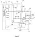
- FIG. 5 An alternative embodiment is depicted in figure 5 .
- This embodiment is similar to the embodiment of figure 4 and like parts have been provided with like reference numerals.
- the current load control circuit 53 takes a different form.
- the first resistor 533 is not used but a resistor 532d is provided instead to provide a tail current.
- the control switch device 532 is supplemented with a further control switch device 532a.
- the further control switch device 532a may be a transistor device and may be a PNP transistor device.
- the emitters of the control switch device 532 and further control switch device 532a may be connected together in electrical communication and coupled via the resistor 532d to the ignition or other current load line 34.
- the base of the further control switch device 532a may be coupled in electrical communication with the ground line and, via a first resistor 532c (to provide a bias and base current for the further control switch device 532a).
- the base of the further control switch device 532a may be further coupled in electrical communication via a Zener diode 532b to the ignition or other current load line 34.
- a bandgap diode e.g. the Zener diode 532b
- the coupling capacitor 5121 of the drive circuit 512 of the switching boost converter 51 may be provided. This coupling capacitor 5121 may be provided to seek to improve switching efficiency, for example.
- the embodiments of figures 4a , 4b and 5 provide a regulated current load control circuit 53.
- the regulated current load control circuit 53 of figure 5 is more tolerant to variations in the voltage of the ignition or other current load line 34 and/or temperature variations than the embodiments of figures 4a and 4b .
- Figure 5 shows the provision of both the diode 514 and the rectifier circuit 52. As discussed above, in some variations only one of the diode 514 and rectifier circuit 52 may be provided.
- the load recovery circuit 22/42 may be used as a braking system load recovery circuit 22 or a lighting system load recovery circuit 42.
- a vehicle 1 may include one or more such load recovery circuits 22/42.
- the truck 11 may include one or more such load recovery circuits 22/42.
- the trailer 12 may include one or more such load recovery circuits 22/42.
- Embodiments of the invention have been described with reference to lighting and braking systems. However, it will be appreciated that embodiments may be used in relation to other elements and systems which are configured to be connected to the electrical supply system of a vehicle.
- the current drawn from the ignition or other current load line 34 is less than 100mA. In some embodiments, the current drawn from the ignition or other current load line 34 is about 80mA.
- the load recovery circuit 22/42 of some embodiments may be configured to return a substantial part of this current to the return battery line 55 (for example, about 85%-95% of the load current from the current load line 34 may be returned in some embodiments). In some other embodiments, e.g. for lighting applications, the current from the current load line 34 could be higher with, in some embodiments, a similar proportion returned.
- the operation of the current load circuit 22/42 of embodiments provides a regulated current load which may use pulse width modulation to maintain a substantially constant current load via an inductor 513 which is used to provide a return current.
- the return line has been described as a battery return line 55, the return line could be for another part of the vehicle electrical supply system 3.
- the terms "comprises” and “comprising” and variations thereof mean that the specified features, steps or integers are included. The terms are not to be interpreted to exclude the presence of other features, steps or components.
Landscapes
- Engineering & Computer Science (AREA)
- Mechanical Engineering (AREA)
- Power Engineering (AREA)
- Transportation (AREA)
- Automation & Control Theory (AREA)
- Dc-Dc Converters (AREA)
Description
- Embodiments of the present invention relate to a current load circuit for a vehicle, a vehicle electrical supply system, and a vehicle. In some embodiments, the current load circuit provides a regulated load for a vehicle electrical system so that a control device of the vehicle correctly detects the presence of an element whilst the current load circuit dissipates less power than some conventional circuits.
- Some vehicle electrical systems (such as an antilock brake system for a trailer configured to be towed by a truck) require a defined current load in order to confirm the correct operation or connection of one or more parts of the electrical system. For example, some vehicle braking systems for vehicles comprising a truck and trailer combination require a current load to be applied to the truck ignition line in order to confirm the connection of a braking system of the trailer. This load may be required during the starting of the vehicle as well as for a period of operation of the vehicle (e.g. as the vehicle is travelling).
- Accordingly, a resistor is commonly used to provide the current load. For example, a braking system of a trailer may include a resistor which draws current from the ignition line when the braking system of the trailer is connected to the truck.
- Other instances in which this may occur includes parts of the vehicle electrical system which were originally designed for incandescent lamp. Many such systems require a relatively large current to be drawn by the incandescent lamp in order to indicate that a working incandescent lamp has been connected correctly. Subsequent retrofitting of LED lamps, however, mean that the same magnitude of current is no longer drawn and the vehicle electrical system may, therefore, cease the supply of electrical power to the lamp and/or issue an indication that the lamp is not functioning. This is conventionally resolved by providing a ballast resistor.
- The resistors used in these examples draw current sufficient to satisfy the requirements of the vehicle electrical system but often perform no other useful function. A significant amount of power may be dissipated through the resistors.
- Therefore, for the braking system example, a resistor value may be selected based on a cranking voltage of the vehicle (to ensure that the current load is sufficiently high even when the voltage on the ignition line is relatively low). However, the voltage on the ignition line will be much higher at other times (such as when a battery of the vehicle is being charged, e.g. using an alternator or other charging system). These periods of operation at a higher voltage may be much longer than the periods during which the ignition line is at a lower voltage. Therefore, the current drawn by the resistor may be higher than is necessary for a long period of time. For example, the current load required by the vehicle electrical system may be 80mA and the vehicle cranking voltage may be 16V. Therefore, a resistor of 200 Ohms would be needed (i.e. 16/0.08). However, during charging, the ignition line voltage may be 32V. Thus, the power loss through the resistor would be 5W (i.e. 322/200), which may be dissipated for substantially the entire time the vehicle is operating.
- In both examples, the resistors dissipate the power as waste heat. Typically, the higher the current required, the lower the resistance required and the more power which must be dissipated, requiring a physically larger resistor. Therefore, not only is there an issue of inefficient use of electrical power but there is also an issue with housing/locating the resistors, removal of the heat generated, and, of course, the cost of the resistors.
-
EP2469978 discloses a vehicle energy retrieving device which includes an input current detection circuit, a boost converter circuit, an output voltage detection circuit, a power source and a load end. The input current detection circuit controls input current and the boost converter circuit is electrically connected to the input current detection circuit in series and converts low voltage into high voltage. The output voltage detection circuit controls output voltage when the circuit is an open circuit. The vehicle energy retrieving device retrieves the surplus electric power and recharges the surplus electric power to the power source to improve the shortcomings of the conventional driving computer system so that when braking or driving, the driving computer system does not generate any false signals. -
US 2014247005 discloses an electrical system for a tractor trailer combination. - There is a need, therefore, to alleviate the problems caused by vehicle electrical systems requiring a current load in these and similar circumstances.
- Accordingly, an aspect of the present invention provides a trailer braking system current load circuit configured to provide a predetermined current load on a power line of an electrical supply system of a vehicle, the current load circuit comprising: a switching boost converter configured to be charged from the current load line and to discharge to a return line of the electrical supply system of the vehicle; and a current load control circuit configured to control the operation of the switching boost converter to maintain a current load on the current load line above a predetermined current during operation of the switching boost converter, such that a portion of the current drawn from the current load line is returned to the return line of the electrical supply system of the vehicle.
- The circuit may further comprise a fault detection circuit which is configured to determine whether a voltage on the return line is below a predetermined threshold voltage and to cease operation of the switching boost converter if the voltage on the return line is below the predetermined threshold voltage.
- The current load control circuit may be coupled to a current sense element which is configured to provide the current load control circuit with an indication of the current through an inductor of the switching boost converter.
- The circuit may further comprise a rectifier which is configured to rectify an output of the switching boost converter.
- The rectifier may be a synchronous rectifier which is configured to operate synchronously with the switching boost converter and/or may be an AC coupled rectifier.
- Another aspect provides an electrical supply system of a vehicle, including: a current load line; a return line; a trailer braking system switching boost converter configured to be charged from the current load line and to discharge to the return line; and a trailer braking system current load control circuit configured to control the operation of the switching boost converter to maintain a current load on the current load line above a predetermined current during operation of the switching boost converter, such that a portion of the current drawn from the current load line is returned to the return line of the electrical supply system of the vehicle.
- The electrical supply system may further comprise a fault detection circuit which is configured to determine whether a voltage on the return line is below a predetermined threshold voltage and to cease operation of the switching boost converter if the voltage on the return line is below the predetermined threshold voltage.
- The current load control circuit may be coupled to a current sense element which is configured to provide the current load control circuit with an indication of the current through an inductor of the switching boost converter.
- The electrical supply system may further comprise a rectifier which is configured to rectify an output of the switching boost converter.
- The rectifier may be a synchronous rectifier which is configured to operate synchronously with the switching boost converter and/or may be an AC coupled rectifier.
- The electrical supply system may further comprise a control device which is configured to determine whether an element is connected or correctly connected to the electrical supply system based on the current load on the current load line.
- Another aspect provides a vehicle including an electrical supply system as above, further comprising a braking system.
- The trailer braking system switching boost converter and trailer braking system current load control circuit may form part of the braking system.
- Embodiments of the present invention are described, by way of example only, with reference to the accompanying drawings, in which:
-
Figure 1 shows a schematic representation of a vehicle according to some embodiments; -
Figure 2 shows a schematic representation of a braking system and electrical supply system of some embodiments; -
Figure 3 shows a schematic representation of a control load recovery circuit of some embodiments; -
Figures 4a ,4b , and5 show schematic representations of control load recovery circuits of some embodiments. - In some embodiments, see
figure 1 for example, the present invention includes avehicle 1 to which abraking system 2 has been fitted. Thevehicle 1 may include atruck 11 andtrailer 12, thetrailer 12 being configured to be towed by thetruck 11. Thebraking system 2 may, therefore, include a portion which is part of thetruck 11 and a portion which is part of thetrailer 12. Other configurations ofbraking system 2 andvehicle 1 may, however, be used in other embodiments. - The
braking system 2, with reference tofigure 2 , includes abrake module 21 which is configured, on actuation, to apply a braking force to one or more ground engaging wheels of the vehicle 1 (e.g. of thetruck 11 and/or trailer 12) in order to slow thevehicle 1 and/or substantially prevent its movement. Thebraking system 2 may also include a braking systemload recovery circuit 22. - The
vehicle 1 may, in some embodiments, include alighting system 4 which may be part of thetruck 11, part of thetrailer 12, or part of both thetruck 11 and the trailer 12 (seefigure 2 , for example). Thelighting system 4 may include, for example, one ormore lamps 41 which are configured to light an area or volume around at least part of thevehicle 1 and/or to provide an indication of the operation or intended operation of the vehicle 1 (such as brake lights, turn signals, etc.). Thelighting system 4 may also include a lighting systemload recovery circuit 42. - The
vehicle 1 includes anelectrical supply system 3, seefigure 2 , which is configured to provide electrical power to one or more units of thevehicle 1, including thebraking system 2 and thelighting system 4, if provided. - The
electrical supply system 3 may include abattery 31 and a generation system 32 (such as an electrical alternator or other generator) which is configured to generate electricity using mechanical power generated by an engine of thevehicle 1, for example. Theelectrical supply system 3 may include an ignition or othercurrent load line 34 which is configured, with a ground line, to supply electricity to the one or more units of thevehicle 1. In this instance, the voltage of the electricity supplied through theelectrical supply system 3 may be 12V, 24V, or 32V, for example. The battery 31 - if provided - may be configured to provide electrical power at any one of these voltages. - The
braking system 2 and/or thelighting system 4 are configured to be connected in electrical communication with theelectrical supply system 3 such that electrical power from theelectrical supply system 3 is provided to thebraking system 2 and/orlighting system 4. Accordingly, the ignition or othercurrent load line 34 may be connected to thebraking system 2 and/or thelighting system 4. - The
vehicle 1 may further include one ormore control devices 13 which are each configured to control an aspect of the operation of thevehicle 1. This may include, for example, determining whether the braking system 2 (or a part thereof) is correctly connected. Thus, acontrol device 13 of the one ormore control devices 13 may be configured to determine whether a part of thebraking system 2 associated with thetrailer 12 is correctly connected to a part of thebraking system 2 associated with thetruck 11. Similarly, the one ormore control devices 13 may include a control device which is configured to determine whether a part of thelighting system 4 is correctly fitted and/or operating correctly. Thus, for example, thecontrol device 13 may be configured to determine if alamp 41 is fitted to thelighting system 4 and/or if thelamp 41 is operating correctly. - The or each
control device 13 may use a current load to determine whether the braking system 2 (or a part thereof) is correctly connected and/or to determine if alamp 41 is correctly fitted and/or functioning correctly. - The braking system
load recovery circuit 22 and the lighting systemload recovery circuit 42 may each be configured to provide the current load expected by the associatedcontrol device 13 such that thecontrol device 13 can determine that the braking system 3 (or a part thereof) is correctly connected and/or if thelamp 41 is correctly fitted and/or functioning correctly. - The braking system
load recovery circuit 22 and the lighting systemload recovery circuit 42 may operate in a corresponding manner and embodiments will, therefore, be described with reference to a singleload recovery circuit 22/42 which could be implemented as either of the braking system or lighting systemload recovery circuit 22. Of course, the same or a similarload recovery circuit 22/42 could be used in other situations in which a current load is required in part of avehicle 1 in order to indicate the presence of a part of thevehicle 1, the correct connection of that part, and/or the correct functioning of that part. - With reference to
figure 3 , theload recovery circuit 22/42 is configured to receive electrical power from an ignition or othercurrent load line 34. A currentload control circuit 53 is coupled in electrical communication with the ignition or othercurrent load line 34 and is configured to determine, selectively, whether the electrical power is delivered to a switchingboost converter 51 of theload recovery circuit 22/42. - The switching
boost converter 51 is configured to use the electrical power from the ignition or othercurrent load line 34 in order to provide a return current to abattery return line 55. - The current
load control circuit 53 is further configured to ensure that the current drawn from the ignition or othercurrent load line 34 exceeds a predetermined current load during operation of the switchingboost converter 51. The currentload control circuit 53 may be further configured to control the operation of the switchingboost converter 51 to moderate the current drawn from the ignition or other current load line 34 (i.e. the current load) is greater than the predetermined current load and may be configured to control the operation of the switchingboost converter 51 to moderate the current drawn from the ignition or othercurrent load line 34 below a further predetermined current load. In some embodiments, the currentload control circuit 53 is configured to ensure that the current drawn from the ignition or othercurrent load line 34 is substantially the predetermined current load during operation of the switchingboost converter 51. Accordingly, when the switchingboost converter 51 is being discharged (i.e. aninductor 513 of the switchingboost converter 51 is discharging), the currentload control circuit 53 may couple a resistive load to the ignition or othercurrent load line 34 to maintain the current load on the ignition or othercurrent load line 34. In some embodiments, the current drawn from the ignition or othercurrent load line 34 may be substantially continuous but may include a degree of ripple. The current is, as will be understood, pulsed in thebattery return line 55 during operation of embodiments. - The switching
boost converter 51 may be connected in electrical communication with arectifier circuit 52 which may be configured to ensure that the output voltage of the switchingboost converter 51 with respect to the ground line is the correct polarity to charge abattery 31 connected to the battery return line 55 - i.e. a positive voltage with respect to the ground line. - The
rectifier circuit 52 may, accordingly, also form part of theload recovery circuit 22/42. - The
load recovery circuit 22/42 may further include afault detection circuit 54 which is configured to detect a fault situation and to terminate operation of the switchingboost converter 51 in the event of a detected fault situation. In particular, thefault detection circuit 54 may be configured to detect a low voltage on the battery return line 55 (with respect to the ground line) which may indicate, for example, that thebattery 31 has become disconnected, discharged or is faulty. In such a fault situation, operation of the switchingboost converter 51 is ceased with the aim of reducing the risk of theload recovery circuit 22/42 becoming the main source of electrical power for one or more other parts of thevehicle 1. - Thus, in operation, the current
load control circuit 53 operates to maintain a current load which is greater than or equal to the predetermined current load, whilst operating the switchingboost converter 51 to return a part of the electrical power drawn from the ignition or other current load line to abattery return line 55 to which thebattery 31 may be connected. As such, compared to many prior systems, this arrangement may result in less wasted power, for example. The efficiency of the operation of some embodiments may be over 90% in some instances, so instead of 5W dissipated by some conventional systems the power dissipated may be as low as about 0.5W. - Accordingly, reference is now made to the example embodiment in
figure 4 with this figure used to describe the operation of the depicted embodiment but also other embodiments of the invention. - In this example embodiment, the current
load control circuit 53 includes acurrent sense element 531 which may be configured to sense the current draw by the switching boost converter 51 (e.g. in the charging of aninductor 513 thereof). Thecurrent sense element 531 may be coupled to acontrol switch device 532 of the currentload control circuit 53 which is configured to be actuated between an on and an off state. When in the on-state, thecontrol switch device 532 is configured to couple the ignition or othercurrent load line 34 in electrical communication with the switchingboost converter 51 and, in particular, with adrive circuit 512 of the switchingboost converter 51. When in the off-state, thecontrol switch device 532 is configured to disconnect the ignition or othercurrent load line 34 from the switchingboost converter 51 and, in particular, from thedrive circuit 512 of the switchingboost converter 51. - In some embodiments, the
current sense element 531 is a relatively low value resistor (e.g. 7.5 or 15 Ohms) and thecontrol switch device 532 is a transistor device which may be a PNP transistor. Thecurrent sense element 531 may, therefore, be connected between the base of thecontrol switch device 532 and the ignition or othercurrent load line 34. The emitter of thecontrol switch device 532 may be connected to the ignition or othercurrent load line 34 and the collector of thecontrol switch device 532 may be connected to the ground line via one or more resistors. The one or more resistors may include afirst resistor 533 and asecond resistor 534, such that the switching boost converter 51 (e.g. thedrive circuit 512 of the switching boost converter 51) is connected in electrical communication between the first and second resistors 533,534 - which may, as will be understood, form part of a level translator. - The base of the
control switch device 532 may be further connected to the switchingboost converter 51 and, in particular, to theinductor 513 of the switchingboost converter 51. - When the
inductor 513 of the switchingboost converter 51 is uncharged or below an energy threshold, as determined by thecurrent sense element 531, thecontrol switch device 532 is in its off-state. In other words, as the current through thecurrent sense element 531 is less than a threshold current (set by the resistance of the current sense element), thecontrol switch device 532 is in its off-state. As the level of energy stored in theinductor 513 rises, the current through thecurrent sense element 531 will increase until the threshold current is exceeded. This will cause thecontrol switch device 532 to adopt its on-state. - With the
control switch device 532 in its on-state, the switchingboost converter 51 will discharge theinductor 513 to the return line 55 - as described below. - The switching
boost converter 51 may include thedrive circuit 512 which is configured to drive the operation of amain switch device 511 of the switching boost converter 51 - themain switch device 511 controlling whether theinductor 513 is charged or discharged. As will be appreciated, theinductor 513 in the switchingboost converter 51 is an example of an energy storage element configured to be charged and discharged during operation of the switchingboost converter 51. - The
current drive circuit 512 may include adrive switch device 5122 which is configured to control the operation of themain switch device 511 of the switchingboost converter 51. Accordingly, thedrive switch device 5122 may include a transistor device. Thedrive switch device 5122 may be connected to the ignition or other current load line via at least part of thefault detection circuit 54. - In some embodiments, the
drive switch device 5122 is a transistor device which may be an NPN transistor. The emitter of thedrive switch device 5122 may be connected in electrical communication with the ground line, and the collector of thedrive switch device 5122 may be connected in electrical communication with thefault detection circuit 54, which may be via aresistor 5123. The base of thedrive switch device 5122 may be coupled in electrical communication with the currentload control circuit 53 such that the currentload control circuit 53 is configured to control its operation. The connection of the base of thedrive switch device 5122 may be to the potential divider formed by the first and second resistors 533,534 of the currentload control circuit 53, for example. - Accordingly, as will be understood, the actuation of the
drive switch device 5122 between an on and an off state is controlled by the currentload control circuit 53. - A
coupling capacitor 5121 of thedrive circuit 512 may couple the base of thedrive switch device 5122 to the collector of the main switch device 511 - see below. Thecoupling capacitor 5121, if included, provides positive feedback which speeds up the switching of themain switch device 511 and which may improve efficiency. - The
main switch device 511 is configured to be actuated by on and off states by thedrive switch device 5122. With thedrive switch device 5122 in its on-state (determined by thecontrol switch device 532 being in its on-state), themain switch device 511 is configured to be in its off-state. With thedrive switch device 5122 in its off-state (determined by thecontrol switch device 532 being in its off-state), themain switch device 511 is configured to be in its on-state. - When in the on-state, the
main switch device 511 is configured to cause the charging of theinductor 513 of the switchingboost converter 51 and, when in the off-state, themain switch device 511 is configured to cause the discharging of theinductor 513 of the switchingboost converter 51. - The
main switch device 511 may be a transistor device and may be an NPN transistor. The emitter of themain switch device 511 may be connected in electrical communication with the ground line, the base may be connected in electrical communication with the collector of thedrive switch device 5122, and the collector may be connected in electrical communication with theinductor 513. - The switching
boost converter 51 may include a diode 514 (seefigure 4b ) which is also connected in electrical communication with theinductor 513, and the main switch device 511 (e.g. with the collector thereof). Thediode 514 may also be connected in electrical communication with thebattery return line 55. - In some embodiments, a
rectifier circuit 52 is provided instead of or in addition to the diode 514 (seefigure 4a ). Therectifier circuit 52 may be configured to operate synchronously with the switchingboost converter 51. In some embodiments, therectifier circuit 52 is an AC coupled synchronous rectifier. - Accordingly, in some embodiments, the
rectifier circuit 52 is configured to be actuated to an on-state (in which a current is permitted to pass to the battery return line 55) by an output of themain switch device 511. As such, therectifier circuit 52 may include anactive switch device 521 which is coupled to themain switch device 511 and configured to be actuated in accordance therewith. This coupling may be via acapacitor 522. Theactive switch device 521 may be a transistor device and may be an NPN transistor. Accordingly the base of theactive switch device 521 may be coupled in electrical communication with the collector of themain switch device 511, e.g. via thecapacitor 522. The base and the emitter of theactive switch device 521 may be coupled in electrical communication via aresistor 523, for example. The emitter of theactive switch device 521 may be further connected in electrical communication with thebattery return line 55 and the collector of theactive switch device 521 may be connected in electrical communication with theinductor 513 such that, when theactive switch device 521 is in its on-state current is allowed to pass from theinductor 513, through therectifier circuit 52, and to thebattery return line 55. - The
diode 514 also, as will be understood, serves as a rectification circuit. Therefore, may be referred to herein as an alternative to therectifier circuit 52 and references to therectifier circuit 52 may be references to a rectifier circuit of which therectifier circuit 52 infigure 4a is one example and thediode 514 offigure 4b is another. - When the
main switch device 511 is in its on-state, theactive switch device 521 may be in its off-state (such that theinductor 513 does not discharge through thediode 514/rectifier circuit 52) and with themain switch device 511 in its off-state, current may pass through thediode 514 or theactive switch device 521 may be in its on-state and current may pass therethrough to thereturn line 55. - As will be appreciated, with the
control switch device 532 is in its off-state, thedrive switch device 5122 is in its off-state (as a result of the second resistor 534). Themain switching device 511 is consequently in its on-state by virtue of the current through the fault detection circuit 54 (e.g. through ashutdown switch device 542, see below) and theresistor 5123. - The current through the
inductor 513 rises and, when the current through thecurrent sense element 531 increases to exceed the threshold current, this will cause thecontrol switch device 532 to adopt its on-state. - With the
control switch device 532 in its on-state, thedrive switch device 5122 will be actuated to its on-state which, in turn, causes themain switch device 511 to actuate to its off-state. - The energy in the
inductor 513 will dissipate by delivering current to therectifier circuit 52 and/or thediode 514. The current through therectifier circuit 52 and/ordiode 514 will, therefore, rise as the energy stored in theinductor 513 decays. Accordingly, theinductor 513 returns current to the return line 55 (e.g. through therectifier circuit 52 and/or diode 514). - As a result of the operation of some embodiments, the current drawn from the
current load line 34 is substantially continuous but the current returned to thebattery return line 55 is intermittent (but at a higher voltage). - The
fault detection circuit 54 is configured to compare a voltage on thebattery return line 55 with a further voltage (which may be a predetermined voltage and/or which may be dependent on the voltage of the ignition or other current load line 34). If the voltage on thebattery return line 55 is sufficiently low, then thefault detection circuit 54 is configured to cease the operation of themain switch device 511. This may be achieved, for example, by altering the operation of the drive circuit 512 (e.g. the drive switch device 5122). In particular, thefault detection circuit 54 may be configured to disconnect the collector of thedrive switch device 5122 from the ignition or othercurrent load line 34 on detection of a fault. - The
fault detection circuit 54 may include ashutdown switch device 542 which is configured to cause the operation of themain switch device 511 to cease and may include a driveshutdown switch device 543 which is configured to drive the operation of theshutdown switch device 542. The shutdown and drive shutdown switch devices 542,543 may include transistor devices and may both be PNP transistors. - Accordingly, the emitter of the
shutdown switch device 542 may be connected in electrical communication with the ignition or othercurrent load line 34, the collector of theshutdown switch device 542 may be connected in electrical communication with the main switch device 511 (e.g. the base thereof and may be via the resistor 5123) and the drive circuit 512 (e.g. with thedrive switch device 5122 and maybe with the collector thereof, and maybe via the resistor 5123). The base of theshutdown switch device 542 may be connected in electrical communication with the drive shutdown switch device 543 (e.g. in particular, with the collector thereof). The collector of the driveshutdown switch device 543 may be further connected in electrical communication with the ground line (e.g. via a resistor 544), and the emitter may be connected in electrical communication with the ignition or othercurrent load line 34. The base of the driveshutdown switch device 543 may be connected in electrical communication with a reference voltage and thebattery return line 55. The reference voltage may be provided by the ignition or othercurrent load line 34. If the battery return line voltage is sufficiently high, then the driveshutdown switch device 543 controls theshutdown switch device 542 to maintain the operation of themain switch device 511 and, hence, the switchingboost converter 51. If, however, the battery return line voltage drops sufficiently, then the driveshutdown switch device 543 controls theshutdown switch device 542 to cease the operation of themain switch device 511 and, hence, the switchingboost converter 51. Accordingly, the base of the driveshutdown switch device 543 may be connected in electrical communication with thebattery return line 55, via afirst resistor 545 to the ignition or othercurrent load line 34, and via asecond resistor 546 to the ground line. - A
protective diode 541 and returnline resistor 547 may be provided in series on thebattery return line 55 between therectifier circuit 52 connection to thebattery return line 55 and rest of thefault detection circuit 54. If thebattery return line 55 voltage is sufficiently high for the driveshutdown switch device 543 to control theshutdown switch device 542 to maintain the operation of themain switch device 511 and, hence, the switchingboost converter 51, then theprotective diode 541 will not conduct. - In some embodiments, the
fault detection circuit 54 may be configured to turn off theshutdown switch device 542, if thecurrent load line 34 voltage exceeds a voltage threshold (this may occur, for example, as a result of load dump transients). In some embodiments, the voltage threshold may be defined by a plurality of resistors - such as thefirst resistor 545 and the second resistor 546 - which may form a potential divider. - Accordingly, if the voltage of
current load line 34 exceeds the threshold voltage then the driveshutdown switch device 543 controls theshutdown switch device 542 to cease the operation of themain switch device 511 and, hence, the switchingboost converter 51. - As will be appreciated, in accordance with some embodiments, the current load is provided on the ignition or other
current load line 34 and yet a portion of the current is returned to the battery return line 55 - to recharge thebattery 31. Accordingly, some embodiments provide more energy efficient mechanisms for providing the current load than some prior systems. In addition, some embodiments eliminate or substantially reduce the need to provide large ballast resistors in order to achieve the required current load. Furthermore, some embodiments, provide the current load over a relatively wide range of voltages on thecurrent load line 34 and/or returnline 55, such that the current load is provided during the voltages on the ignition or othercurrent load line 34 which are likely to be encountered during cranking of thevehicle 1 and also during normal operation of the vehicle 1 - that current load being the predetermined current load and substantially the same over this range of voltages. - The
fault detection circuit 54 which may be included in some embodiments, helps to ensure that theload recovery circuit 22/42 is not used to power unintended parts of thevehicle 1 which may draw an excessive current from theload recovery circuit 22/42 if thebattery 31 is not present or is overly discharged and/or to disable theload recovery circuit 22/41 if thecurrent load line 34 and/or returnline 55 voltage exceeds a respective threshold. - An alternative embodiment is depicted in
figure 5 . This embodiment is similar to the embodiment offigure 4 and like parts have been provided with like reference numerals. However, in accordance with this embodiment, and some other embodiments, the currentload control circuit 53 takes a different form. In particular, thefirst resistor 533 is not used but aresistor 532d is provided instead to provide a tail current. Thecontrol switch device 532 is supplemented with a furthercontrol switch device 532a. Again the furthercontrol switch device 532a may be a transistor device and may be a PNP transistor device. The emitters of thecontrol switch device 532 and furthercontrol switch device 532a may be connected together in electrical communication and coupled via theresistor 532d to the ignition or othercurrent load line 34. The base of the furthercontrol switch device 532a may be coupled in electrical communication with the ground line and, via afirst resistor 532c (to provide a bias and base current for the furthercontrol switch device 532a). The base of the furthercontrol switch device 532a may be further coupled in electrical communication via aZener diode 532b to the ignition or othercurrent load line 34. Accordingly, in some embodiments, a bandgap diode (e.g. theZener diode 532b) is provided to achieve a regulated current drawn from the ignition or othercurrent load line 34. In addition, in this and some other embodiments, thecoupling capacitor 5121 of thedrive circuit 512 of the switching boost converter 51 (see above) may be provided. Thiscoupling capacitor 5121 may be provided to seek to improve switching efficiency, for example. - The embodiments of
figures 4a ,4b and5 , and some other embodiments, provide a regulated currentload control circuit 53. In some embodiments, the regulated currentload control circuit 53 offigure 5 is more tolerant to variations in the voltage of the ignition or othercurrent load line 34 and/or temperature variations than the embodiments offigures 4a and4b . -
Figure 5 shows the provision of both thediode 514 and therectifier circuit 52. As discussed above, in some variations only one of thediode 514 andrectifier circuit 52 may be provided. - As explained above, the
load recovery circuit 22/42 may be used as a braking systemload recovery circuit 22 or a lighting systemload recovery circuit 42. - A
vehicle 1 may include one or more suchload recovery circuits 22/42. In some embodiments, thetruck 11 may include one or more suchload recovery circuits 22/42. In addition or alternatively, thetrailer 12 may include one or more suchload recovery circuits 22/42. - Embodiments of the invention have been described with reference to lighting and braking systems. However, it will be appreciated that embodiments may be used in relation to other elements and systems which are configured to be connected to the electrical supply system of a vehicle.
- In some embodiments, the current drawn from the ignition or other
current load line 34 is less than 100mA. In some embodiments, the current drawn from the ignition or othercurrent load line 34 is about 80mA. Theload recovery circuit 22/42 of some embodiments may be configured to return a substantial part of this current to the return battery line 55 (for example, about 85%-95% of the load current from thecurrent load line 34 may be returned in some embodiments). In some other embodiments, e.g. for lighting applications, the current from thecurrent load line 34 could be higher with, in some embodiments, a similar proportion returned. - As will be appreciated, therefore, the operation of the
current load circuit 22/42 of embodiments provides a regulated current load which may use pulse width modulation to maintain a substantially constant current load via aninductor 513 which is used to provide a return current. - Although the return line has been described as a
battery return line 55, the return line could be for another part of the vehicleelectrical supply system 3. When used in this specification and claims, the terms "comprises" and "comprising" and variations thereof mean that the specified features, steps or integers are included. The terms are not to be interpreted to exclude the presence of other features, steps or components.
Claims (13)
- A trailer braking system current load circuit (22,42) configured to provide a predetermined current load on a current load line (34) of an electrical supply system of a vehicle (1), the current load circuit (22,42) comprising:a switching boost converter (51) configured to be charged from the current load line (34) and to discharge to a return line (55) of the electrical supply system of the vehicle (1); anda current load control circuit (53) configured to control the operation of the switching boost converter (51) to maintain a current load on the current load line (34) above a predetermined current during operation of the switching boost converter (51), such that a portion of the current drawn from the current load line (34) is returned to the return line (55) of the electrical supply system of the vehicle (1).
- A circuit (22,42) according to claim 1, further comprising a fault detection circuit (54) which is configured to determine whether a voltage on the return line (55) is below a predetermined threshold voltage and to cease operation of the switching boost converter (51) if the voltage on the return line (55) is below the predetermined threshold voltage.
- A circuit (22,42) according to claim 1 or 2, wherein the current load control circuit (53) is coupled to a current sense element (531) which is configured to provide the current load control circuit (53) with an indication of the current through an inductor of the switching boost converter (51).
- A circuit (22,42) according to any preceding claim, further comprising a rectifier (52) which is configured to rectify an output of the switching boost converter (51).
- A circuit (22,42) according to claim 4, wherein the rectifier (52) is a synchronous rectifier (52) which is configured to operate synchronously with the switching boost converter (51) and/or is an AC coupled rectifier (52).
- An electrical supply system of a vehicle (1), including:a current load line (34);a return line (55);a trailer braking system switching boost converter (51) configured to be charged from the current load line (34) and to discharge to the return line (55); anda trailer braking system current load control circuit (53) configured to control the operation of the switching boost converter (51) to maintain a current load on the current load line (34) above a predetermined current during operation of the switching boost converter (51), such that a portion of the current drawn from the current load line (34) is returned to the return line (55) of the electrical supply system of the vehicle (1).
- An electrical supply system according to claim 6, further comprising a fault detection circuit (54) which is configured to determine whether a voltage on the return line (55) is below a predetermined threshold voltage and to cease operation of the switching boost converter (51) if the voltage on the return line is below the predetermined threshold voltage.
- An electrical supply system according to claim 6 or 7, wherein the current load control circuit (53) is coupled to a current sense element (531) which is configured to provide the current load control circuit (53) with an indication of the current through an inductor of the switching boost converter (51).
- An electrical supply system according to any of claims 6 to 8, further comprising a rectifier (52) which is configured to rectify an output of the switching boost converter (51).
- An electrical supply system according to claim 9, wherein the rectifier (52) is a synchronous rectifier (52) which is configured to operate synchronously with the switching boost converter (51) and/or is an AC coupled rectifier (52).
- An electrical supply system according to any of claims 6 to 10, further comprising a control device (13) which is configured to determine whether an element is connected or correctly connected to the electrical supply system based on the current load on the current load line (34).
- A vehicle (1) including an electrical supply system according to any of claims 6 to 11, further comprising a braking system (2).
- A vehicle according to claim 12, wherein the trailer braking system switching boost converter (51) and trailer braking system current load control circuit (22,42) form part of the braking system (2).
Applications Claiming Priority (2)
| Application Number | Priority Date | Filing Date | Title |
|---|---|---|---|
| GB1605641.8A GB2548924B (en) | 2016-04-01 | 2016-04-01 | A current load circuit, electrical supply system and vehicle |
| PCT/GB2017/050927 WO2017168179A1 (en) | 2016-04-01 | 2017-03-31 | A current load circuit, electrical supply system and vehicle |
Publications (3)
| Publication Number | Publication Date |
|---|---|
| EP3436311A1 EP3436311A1 (en) | 2019-02-06 |
| EP3436311B1 true EP3436311B1 (en) | 2024-12-04 |
| EP3436311B8 EP3436311B8 (en) | 2025-01-08 |
Family
ID=58489741
Family Applications (1)
| Application Number | Title | Priority Date | Filing Date |
|---|---|---|---|
| EP17716004.1A Active EP3436311B8 (en) | 2016-04-01 | 2017-03-31 | A current load circuit, electrical supply system and vehicle |
Country Status (3)
| Country | Link |
|---|---|
| EP (1) | EP3436311B8 (en) |
| GB (1) | GB2548924B (en) |
| WO (1) | WO2017168179A1 (en) |
Citations (2)
| Publication number | Priority date | Publication date | Assignee | Title |
|---|---|---|---|---|
| US20070152502A1 (en) * | 2005-11-18 | 2007-07-05 | Kinsey Gregory W | Power supply control system for a vehicle trailer |
| US7642743B1 (en) * | 2005-12-19 | 2010-01-05 | Cooper Technologies Company | Charger for remote battery |
Family Cites Families (4)
| Publication number | Priority date | Publication date | Assignee | Title |
|---|---|---|---|---|
| DE102004027676B4 (en) * | 2004-04-30 | 2006-06-14 | Siemens Ag | Method and device for testing at least one LED string |
| PL2390140T3 (en) * | 2007-06-01 | 2015-12-31 | Conwys Ag | Switching assembly |
| DE102009052690B3 (en) * | 2009-11-11 | 2011-04-28 | Osma Gmbh | Method for driving LED-lamp of electrical system of e.g. commercial vehicle, involves providing measured flow current as control value to booster, and regulating additional load by measured flow current that is supplied to battery |
| EP2469978A1 (en) * | 2010-12-22 | 2012-06-27 | Long Jing International Technology Enterprise Co., Ltd. | Vehicle energy retrieving device |
-
2016
- 2016-04-01 GB GB1605641.8A patent/GB2548924B/en active Active
-
2017
- 2017-03-31 EP EP17716004.1A patent/EP3436311B8/en active Active
- 2017-03-31 WO PCT/GB2017/050927 patent/WO2017168179A1/en not_active Ceased
Patent Citations (2)
| Publication number | Priority date | Publication date | Assignee | Title |
|---|---|---|---|---|
| US20070152502A1 (en) * | 2005-11-18 | 2007-07-05 | Kinsey Gregory W | Power supply control system for a vehicle trailer |
| US7642743B1 (en) * | 2005-12-19 | 2010-01-05 | Cooper Technologies Company | Charger for remote battery |
Also Published As
| Publication number | Publication date |
|---|---|
| EP3436311B8 (en) | 2025-01-08 |
| GB2548924B (en) | 2022-01-26 |
| EP3436311A1 (en) | 2019-02-06 |
| WO2017168179A1 (en) | 2017-10-05 |
| GB2548924A (en) | 2017-10-04 |
Similar Documents
| Publication | Publication Date | Title |
|---|---|---|
| US9266482B2 (en) | Onboard power supply system and method for operating the onboard power supply system | |
| JP6068465B2 (en) | Transient voltage interruption for power converters | |
| CN104228587B (en) | Intelligent electric power allocation unit | |
| EP2732524A1 (en) | Automatic power converter bypass | |
| US20160229298A1 (en) | Battery power integration apparatus and hev power system having the same | |
| TWI513131B (en) | Voltage regulator and its over-voltage protection circuit | |
| JP2008511277A (en) | Voltage controller with overvoltage protection | |
| CN220254151U (en) | Discharge system for electric vehicle and electric vehicle comprising same | |
| US20150367737A1 (en) | Vehicle control device | |
| CN113300327A (en) | Undervoltage protection apparatus and method | |
| JP2006311775A (en) | Load driving device and vehicle equipped with the same | |
| US10525913B2 (en) | Electronic control device | |
| JP2003209968A (en) | Power supply | |
| JP2003111496A (en) | Exterior regulator for vehicle generator | |
| EP3436311A1 (en) | A current load circuit, electrical supply system and vehicle | |
| US20180278145A1 (en) | Overboost Suppressing Circuit for Boost Converter | |
| CN219583994U (en) | Battery management unit and vehicle | |
| CN118783800A (en) | Method for operating an energy supply circuit of an inverter to control a motor, calculation unit, energy supply circuit of an inverter, and inverter | |
| CN107000662B (en) | Method for controlling electrical consumers of a low-voltage on-board electrical network | |
| US10879719B2 (en) | Regulator control circuit | |
| CN210839510U (en) | Fault protection circuit and fault protection device | |
| US7224561B2 (en) | Protective circuit and method for operating said protective circuit, in particular for overvoltage protection for an electronic control system for a motor vehicle | |
| KR20240039464A (en) | Power stabilizing apparatus for vehicles | |
| CN221574880U (en) | Power supply reverse connection preventing circuit, power supply circuit of vehicle-mounted electric appliance and vehicle | |
| JPS6356135A (en) | Auxiliary storage battery charging device |
Legal Events
| Date | Code | Title | Description |
|---|---|---|---|
| STAA | Information on the status of an ep patent application or granted ep patent |
Free format text: STATUS: UNKNOWN |
|
| STAA | Information on the status of an ep patent application or granted ep patent |
Free format text: STATUS: THE INTERNATIONAL PUBLICATION HAS BEEN MADE |
|
| PUAI | Public reference made under article 153(3) epc to a published international application that has entered the european phase |
Free format text: ORIGINAL CODE: 0009012 |
|
| STAA | Information on the status of an ep patent application or granted ep patent |
Free format text: STATUS: REQUEST FOR EXAMINATION WAS MADE |
|
| 17P | Request for examination filed |
Effective date: 20180928 |
|
| AK | Designated contracting states |
Kind code of ref document: A1 Designated state(s): AL AT BE BG CH CY CZ DE DK EE ES FI FR GB GR HR HU IE IS IT LI LT LU LV MC MK MT NL NO PL PT RO RS SE SI SK SM TR |
|
| AX | Request for extension of the european patent |
Extension state: BA ME |
|
| DAV | Request for validation of the european patent (deleted) | ||
| DAX | Request for extension of the european patent (deleted) | ||
| STAA | Information on the status of an ep patent application or granted ep patent |
Free format text: STATUS: EXAMINATION IS IN PROGRESS |
|
| 17Q | First examination report despatched |
Effective date: 20220428 |
|
| GRAP | Despatch of communication of intention to grant a patent |
Free format text: ORIGINAL CODE: EPIDOSNIGR1 |
|
| STAA | Information on the status of an ep patent application or granted ep patent |
Free format text: STATUS: GRANT OF PATENT IS INTENDED |
|
| INTG | Intention to grant announced |
Effective date: 20240829 |
|
| GRAS | Grant fee paid |
Free format text: ORIGINAL CODE: EPIDOSNIGR3 |
|
| GRAA | (expected) grant |
Free format text: ORIGINAL CODE: 0009210 |
|
| STAA | Information on the status of an ep patent application or granted ep patent |
Free format text: STATUS: THE PATENT HAS BEEN GRANTED |
|
| AK | Designated contracting states |
Kind code of ref document: B1 Designated state(s): AL AT BE BG CH CY CZ DE DK EE ES FI FR GB GR HR HU IE IS IT LI LT LU LV MC MK MT NL NO PL PT RO RS SE SI SK SM TR |
|
| REG | Reference to a national code |
Ref country code: GB Ref legal event code: FG4D |
|
| REG | Reference to a national code |
Ref country code: DE Ref legal event code: R081 Ref document number: 602017086521 Country of ref document: DE Owner name: HALDEX AKTIEBOLAG, SE Free format text: FORMER OWNER: HALDEX BRAKE PRODUCTS AKTIEBOLAG, LANDSKRONA, SE Ref country code: CH Ref legal event code: PK Free format text: BERICHTIGUNG B8 Ref country code: CH Ref legal event code: EP |
|
| REG | Reference to a national code |
Ref country code: DE Ref legal event code: R096 Ref document number: 602017086521 Country of ref document: DE |
|
| RAP2 | Party data changed (patent owner data changed or rights of a patent transferred) |
Owner name: HALDEX AKTIEBOLAG |
|
| REG | Reference to a national code |
Ref country code: IE Ref legal event code: FG4D |
|
| REG | Reference to a national code |
Ref country code: LT Ref legal event code: MG9D |
|
| REG | Reference to a national code |
Ref country code: NL Ref legal event code: MP Effective date: 20241204 |
|
| PG25 | Lapsed in a contracting state [announced via postgrant information from national office to epo] |
Ref country code: HR Free format text: LAPSE BECAUSE OF FAILURE TO SUBMIT A TRANSLATION OF THE DESCRIPTION OR TO PAY THE FEE WITHIN THE PRESCRIBED TIME-LIMIT Effective date: 20241204 |
|
| PG25 | Lapsed in a contracting state [announced via postgrant information from national office to epo] |
Ref country code: FI Free format text: LAPSE BECAUSE OF FAILURE TO SUBMIT A TRANSLATION OF THE DESCRIPTION OR TO PAY THE FEE WITHIN THE PRESCRIBED TIME-LIMIT Effective date: 20241204 |
|
| PG25 | Lapsed in a contracting state [announced via postgrant information from national office to epo] |
Ref country code: BG Free format text: LAPSE BECAUSE OF FAILURE TO SUBMIT A TRANSLATION OF THE DESCRIPTION OR TO PAY THE FEE WITHIN THE PRESCRIBED TIME-LIMIT Effective date: 20241204 |
|
| PG25 | Lapsed in a contracting state [announced via postgrant information from national office to epo] |
Ref country code: ES Free format text: LAPSE BECAUSE OF FAILURE TO SUBMIT A TRANSLATION OF THE DESCRIPTION OR TO PAY THE FEE WITHIN THE PRESCRIBED TIME-LIMIT Effective date: 20241204 |
|
| PG25 | Lapsed in a contracting state [announced via postgrant information from national office to epo] |
Ref country code: NO Free format text: LAPSE BECAUSE OF FAILURE TO SUBMIT A TRANSLATION OF THE DESCRIPTION OR TO PAY THE FEE WITHIN THE PRESCRIBED TIME-LIMIT Effective date: 20250304 |
|
| PG25 | Lapsed in a contracting state [announced via postgrant information from national office to epo] |
Ref country code: GR Free format text: LAPSE BECAUSE OF FAILURE TO SUBMIT A TRANSLATION OF THE DESCRIPTION OR TO PAY THE FEE WITHIN THE PRESCRIBED TIME-LIMIT Effective date: 20250305 Ref country code: LV Free format text: LAPSE BECAUSE OF FAILURE TO SUBMIT A TRANSLATION OF THE DESCRIPTION OR TO PAY THE FEE WITHIN THE PRESCRIBED TIME-LIMIT Effective date: 20241204 |
|
| PG25 | Lapsed in a contracting state [announced via postgrant information from national office to epo] |
Ref country code: RS Free format text: LAPSE BECAUSE OF FAILURE TO SUBMIT A TRANSLATION OF THE DESCRIPTION OR TO PAY THE FEE WITHIN THE PRESCRIBED TIME-LIMIT Effective date: 20250304 |
|
| PG25 | Lapsed in a contracting state [announced via postgrant information from national office to epo] |
Ref country code: NL Free format text: LAPSE BECAUSE OF FAILURE TO SUBMIT A TRANSLATION OF THE DESCRIPTION OR TO PAY THE FEE WITHIN THE PRESCRIBED TIME-LIMIT Effective date: 20241204 |
|
| REG | Reference to a national code |
Ref country code: AT Ref legal event code: MK05 Ref document number: 1747854 Country of ref document: AT Kind code of ref document: T Effective date: 20241204 |
|
| PG25 | Lapsed in a contracting state [announced via postgrant information from national office to epo] |
Ref country code: SM Free format text: LAPSE BECAUSE OF FAILURE TO SUBMIT A TRANSLATION OF THE DESCRIPTION OR TO PAY THE FEE WITHIN THE PRESCRIBED TIME-LIMIT Effective date: 20241204 |
|
| PG25 | Lapsed in a contracting state [announced via postgrant information from national office to epo] |
Ref country code: PL Free format text: LAPSE BECAUSE OF FAILURE TO SUBMIT A TRANSLATION OF THE DESCRIPTION OR TO PAY THE FEE WITHIN THE PRESCRIBED TIME-LIMIT Effective date: 20241204 |
|
| PG25 | Lapsed in a contracting state [announced via postgrant information from national office to epo] |
Ref country code: IS Free format text: LAPSE BECAUSE OF FAILURE TO SUBMIT A TRANSLATION OF THE DESCRIPTION OR TO PAY THE FEE WITHIN THE PRESCRIBED TIME-LIMIT Effective date: 20250404 |
|
| PG25 | Lapsed in a contracting state [announced via postgrant information from national office to epo] |
Ref country code: PT Free format text: LAPSE BECAUSE OF FAILURE TO SUBMIT A TRANSLATION OF THE DESCRIPTION OR TO PAY THE FEE WITHIN THE PRESCRIBED TIME-LIMIT Effective date: 20250404 |
|
| PG25 | Lapsed in a contracting state [announced via postgrant information from national office to epo] |
Ref country code: AT Free format text: LAPSE BECAUSE OF FAILURE TO SUBMIT A TRANSLATION OF THE DESCRIPTION OR TO PAY THE FEE WITHIN THE PRESCRIBED TIME-LIMIT Effective date: 20241204 Ref country code: RO Free format text: LAPSE BECAUSE OF FAILURE TO SUBMIT A TRANSLATION OF THE DESCRIPTION OR TO PAY THE FEE WITHIN THE PRESCRIBED TIME-LIMIT Effective date: 20241204 |
|
| PG25 | Lapsed in a contracting state [announced via postgrant information from national office to epo] |
Ref country code: SK Free format text: LAPSE BECAUSE OF FAILURE TO SUBMIT A TRANSLATION OF THE DESCRIPTION OR TO PAY THE FEE WITHIN THE PRESCRIBED TIME-LIMIT Effective date: 20241204 |
|
| PG25 | Lapsed in a contracting state [announced via postgrant information from national office to epo] |
Ref country code: CZ Free format text: LAPSE BECAUSE OF FAILURE TO SUBMIT A TRANSLATION OF THE DESCRIPTION OR TO PAY THE FEE WITHIN THE PRESCRIBED TIME-LIMIT Effective date: 20241204 |
|
| PG25 | Lapsed in a contracting state [announced via postgrant information from national office to epo] |
Ref country code: IT Free format text: LAPSE BECAUSE OF FAILURE TO SUBMIT A TRANSLATION OF THE DESCRIPTION OR TO PAY THE FEE WITHIN THE PRESCRIBED TIME-LIMIT Effective date: 20241204 |
|
| REG | Reference to a national code |
Ref country code: DE Ref legal event code: R097 Ref document number: 602017086521 Country of ref document: DE |
|
| PG25 | Lapsed in a contracting state [announced via postgrant information from national office to epo] |
Ref country code: SE Free format text: LAPSE BECAUSE OF FAILURE TO SUBMIT A TRANSLATION OF THE DESCRIPTION OR TO PAY THE FEE WITHIN THE PRESCRIBED TIME-LIMIT Effective date: 20241204 |
|
| PG25 | Lapsed in a contracting state [announced via postgrant information from national office to epo] |
Ref country code: DK Free format text: LAPSE BECAUSE OF FAILURE TO SUBMIT A TRANSLATION OF THE DESCRIPTION OR TO PAY THE FEE WITHIN THE PRESCRIBED TIME-LIMIT Effective date: 20241204 |
|
| PLBE | No opposition filed within time limit |
Free format text: ORIGINAL CODE: 0009261 |
|
| STAA | Information on the status of an ep patent application or granted ep patent |
Free format text: STATUS: NO OPPOSITION FILED WITHIN TIME LIMIT |
|
| PG25 | Lapsed in a contracting state [announced via postgrant information from national office to epo] |
Ref country code: MC Free format text: LAPSE BECAUSE OF FAILURE TO SUBMIT A TRANSLATION OF THE DESCRIPTION OR TO PAY THE FEE WITHIN THE PRESCRIBED TIME-LIMIT Effective date: 20241204 |
|
| REG | Reference to a national code |
Ref country code: CH Ref legal event code: L10 Free format text: ST27 STATUS EVENT CODE: U-0-0-L10-L00 (AS PROVIDED BY THE NATIONAL OFFICE) Effective date: 20251015 |
|
| REG | Reference to a national code |
Ref country code: CH Ref legal event code: H13 Free format text: ST27 STATUS EVENT CODE: U-0-0-H10-H13 (AS PROVIDED BY THE NATIONAL OFFICE) Effective date: 20251024 |
|
| 26N | No opposition filed |
Effective date: 20250905 |
|
| PG25 | Lapsed in a contracting state [announced via postgrant information from national office to epo] |
Ref country code: LU Free format text: LAPSE BECAUSE OF NON-PAYMENT OF DUE FEES Effective date: 20250331 |
|
| REG | Reference to a national code |
Ref country code: BE Ref legal event code: MM Effective date: 20250331 |
|
| PG25 | Lapsed in a contracting state [announced via postgrant information from national office to epo] |
Ref country code: BE Free format text: LAPSE BECAUSE OF NON-PAYMENT OF DUE FEES Effective date: 20250331 |
|
| PG25 | Lapsed in a contracting state [announced via postgrant information from national office to epo] |
Ref country code: CH Free format text: LAPSE BECAUSE OF NON-PAYMENT OF DUE FEES Effective date: 20250331 |
|
| PG25 | Lapsed in a contracting state [announced via postgrant information from national office to epo] |
Ref country code: IE Free format text: LAPSE BECAUSE OF NON-PAYMENT OF DUE FEES Effective date: 20250331 |
|
| PGFP | Annual fee paid to national office [announced via postgrant information from national office to epo] |
Ref country code: GB Payment date: 20260324 Year of fee payment: 10 |
|
| PGFP | Annual fee paid to national office [announced via postgrant information from national office to epo] |
Ref country code: DE Payment date: 20260204 Year of fee payment: 10 |
|
| PGFP | Annual fee paid to national office [announced via postgrant information from national office to epo] |
Ref country code: FR Payment date: 20260324 Year of fee payment: 10 |