EP3435533A1 - Power supply and control method thereof - Google Patents
Power supply and control method thereof Download PDFInfo
- Publication number
- EP3435533A1 EP3435533A1 EP17188859.7A EP17188859A EP3435533A1 EP 3435533 A1 EP3435533 A1 EP 3435533A1 EP 17188859 A EP17188859 A EP 17188859A EP 3435533 A1 EP3435533 A1 EP 3435533A1
- Authority
- EP
- European Patent Office
- Prior art keywords
- power supply
- bus voltage
- reference value
- power
- average value
- Prior art date
- Legal status (The legal status is an assumption and is not a legal conclusion. Google has not performed a legal analysis and makes no representation as to the accuracy of the status listed.)
- Granted
Links
Images


Classifications
-
- H—ELECTRICITY
- H02—GENERATION; CONVERSION OR DISTRIBUTION OF ELECTRIC POWER
- H02M—APPARATUS FOR CONVERSION BETWEEN AC AND AC, BETWEEN AC AND DC, OR BETWEEN DC AND DC, AND FOR USE WITH MAINS OR SIMILAR POWER SUPPLY SYSTEMS; CONVERSION OF DC OR AC INPUT POWER INTO SURGE OUTPUT POWER; CONTROL OR REGULATION THEREOF
- H02M7/00—Conversion of AC power input into DC power output; Conversion of DC power input into AC power output
- H02M7/02—Conversion of AC power input into DC power output without possibility of reversal
- H02M7/04—Conversion of AC power input into DC power output without possibility of reversal by static converters
-
- H—ELECTRICITY
- H02—GENERATION; CONVERSION OR DISTRIBUTION OF ELECTRIC POWER
- H02M—APPARATUS FOR CONVERSION BETWEEN AC AND AC, BETWEEN AC AND DC, OR BETWEEN DC AND DC, AND FOR USE WITH MAINS OR SIMILAR POWER SUPPLY SYSTEMS; CONVERSION OF DC OR AC INPUT POWER INTO SURGE OUTPUT POWER; CONTROL OR REGULATION THEREOF
- H02M1/00—Details of apparatus for conversion
- H02M1/08—Circuits specially adapted for the generation of control voltages for semiconductor devices incorporated in static converters
- H02M1/088—Circuits specially adapted for the generation of control voltages for semiconductor devices incorporated in static converters for the simultaneous control of series or parallel connected semiconductor devices
-
- H—ELECTRICITY
- H02—GENERATION; CONVERSION OR DISTRIBUTION OF ELECTRIC POWER
- H02M—APPARATUS FOR CONVERSION BETWEEN AC AND AC, BETWEEN AC AND DC, OR BETWEEN DC AND DC, AND FOR USE WITH MAINS OR SIMILAR POWER SUPPLY SYSTEMS; CONVERSION OF DC OR AC INPUT POWER INTO SURGE OUTPUT POWER; CONTROL OR REGULATION THEREOF
- H02M3/00—Conversion of DC power input into DC power output
- H02M3/02—Conversion of DC power input into DC power output without intermediate conversion into AC
- H02M3/04—Conversion of DC power input into DC power output without intermediate conversion into AC by static converters
- H02M3/10—Conversion of DC power input into DC power output without intermediate conversion into AC by static converters using discharge tubes with control electrode or semiconductor devices with control electrode
-
- H—ELECTRICITY
- H02—GENERATION; CONVERSION OR DISTRIBUTION OF ELECTRIC POWER
- H02M—APPARATUS FOR CONVERSION BETWEEN AC AND AC, BETWEEN AC AND DC, OR BETWEEN DC AND DC, AND FOR USE WITH MAINS OR SIMILAR POWER SUPPLY SYSTEMS; CONVERSION OF DC OR AC INPUT POWER INTO SURGE OUTPUT POWER; CONTROL OR REGULATION THEREOF
- H02M7/00—Conversion of AC power input into DC power output; Conversion of DC power input into AC power output
- H02M7/02—Conversion of AC power input into DC power output without possibility of reversal
- H02M7/04—Conversion of AC power input into DC power output without possibility of reversal by static converters
- H02M7/12—Conversion of AC power input into DC power output without possibility of reversal by static converters using discharge tubes with control electrode or semiconductor devices with control electrode
- H02M7/21—Conversion of AC power input into DC power output without possibility of reversal by static converters using discharge tubes with control electrode or semiconductor devices with control electrode using devices of a triode or transistor type requiring continuous application of a control signal
- H02M7/217—Conversion of AC power input into DC power output without possibility of reversal by static converters using discharge tubes with control electrode or semiconductor devices with control electrode using devices of a triode or transistor type requiring continuous application of a control signal using semiconductor devices only
- H02M7/23—Conversion of AC power input into DC power output without possibility of reversal by static converters using discharge tubes with control electrode or semiconductor devices with control electrode using devices of a triode or transistor type requiring continuous application of a control signal using semiconductor devices only arranged for operation in parallel
-
- H—ELECTRICITY
- H02—GENERATION; CONVERSION OR DISTRIBUTION OF ELECTRIC POWER
- H02M—APPARATUS FOR CONVERSION BETWEEN AC AND AC, BETWEEN AC AND DC, OR BETWEEN DC AND DC, AND FOR USE WITH MAINS OR SIMILAR POWER SUPPLY SYSTEMS; CONVERSION OF DC OR AC INPUT POWER INTO SURGE OUTPUT POWER; CONTROL OR REGULATION THEREOF
- H02M1/00—Details of apparatus for conversion
- H02M1/0067—Converter structures employing plural converter units, other than for parallel operation of the units on a single load
- H02M1/007—Plural converter units in cascade
-
- H—ELECTRICITY
- H02—GENERATION; CONVERSION OR DISTRIBUTION OF ELECTRIC POWER
- H02M—APPARATUS FOR CONVERSION BETWEEN AC AND AC, BETWEEN AC AND DC, OR BETWEEN DC AND DC, AND FOR USE WITH MAINS OR SIMILAR POWER SUPPLY SYSTEMS; CONVERSION OF DC OR AC INPUT POWER INTO SURGE OUTPUT POWER; CONTROL OR REGULATION THEREOF
- H02M1/00—Details of apparatus for conversion
- H02M1/0067—Converter structures employing plural converter units, other than for parallel operation of the units on a single load
- H02M1/0074—Plural converter units whose inputs are connected in series
Definitions
- the present disclosure relates to a power supply, and in particular, to a power supply used in a three-phase system.
- a three-phase power device may be implemented from single-phase modules. However, when an artificial floating neutral point is created by using a star configuration in the implementation of the three-phase power device, the instability of the artificial neutral point voltage may cause the three-phase AC power transmission at the grid-side unbalance.
- the power supply includes a plurality of power modules and a control circuit. Input terminals of the power modules are electrically connected in star connection such that each power module receives a corresponding phase input voltage. Output terminals of the plurality of power modules are electrically connected in parallel, in which each power modules includes a first and a second converter.
- the first converter is configured to convert the corresponding phase input voltage into an intermediate bus voltage.
- the second converter is configured to output a DC supply voltage according to the intermediate bus voltage.
- the control circuit is electrically coupled to the power modules and configured to output first driving signals to control the first converters in the power modules, and configured to output second driving signals to control the second converters in the power modules.
- a bus voltage average value is calculated by the control circuit according to the intermediate bus voltages of the power modules, and the first driving signals and the second driving signals for the power modules are generated according to the bus voltage average value.
- the power supply control method includes detecting a plurality of intermediate bus voltages of a plurality of power modules of a power supply respectively; calculating, by a control circuit of the power supply, a bus voltage average value according to the intermediate bus voltages of the power modules; outputting, by the control circuit, a plurality of first driving signals according to the bus voltage average value to respectively control a plurality of first converters in the power modules; and outputting, by the control circuit, a plurality of second driving signals according to the bus voltage average value to respectively control a plurality of second converters in the power modules.
- Coupled may also be termed “electrically coupled,” and the term “connected” may be termed “electrically connected.” “Coupled” and “connected” may also be used to indicate that two or more elements cooperate or interact with each other. It will be understood that, although the terms “first,” “second,” etc., may be used herein to describe various elements, these elements should not be limited by these terms. These terms are used to distinguish one element from another. For example, a first element could be termed a second element, and, similarly, a second element could be termed a first element, without departing from the scope of the embodiments.
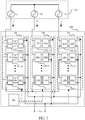
- Fig.1 is a diagram illustrating a power supply 100 according to some embodiments of the present disclosure. As shown in Fig. 1 , the power supply 100 is used in a three-phase power system, and configured to receive a three-phase input power, and correspondingly output a DC supply voltage Vo.
- the power supply 100 includes three single-phase power modules Ma, Mb, and Mc and a control circuit 160.
- Input terminals of the power modules Ma, Mb, and Mc are electrically connected in star connection such that each of the power modules Ma, Mb, and Mc is configured to receive a corresponding phase input voltage Va, Vb, or Vc and a corresponding phase input current Ia, Ib, or Ic.
- Output terminals of the power modules Ma, Mb, and Mc are electrically connected in parallel.
- the star connection at the input side of the power modules Ma, Mb, and Mc creates the artificial neutral point Ny in the power supply 100 which needs to be balanced against the actual neutral point N0 of the grid.
- the single-phase power modules Ma, Mb, and Mc may now be used in the power supply 100 for three-phase configuration.
- each of the power modules Ma, Mb, and Mc respectively includes an AC-DC converter 120a, 120b, 120c and a DC-DC converter 140a, 140b, 140c.
- the AC-DC converters 120a, 120b, 120c are configured to convert the corresponding phase input voltage Va, Vb, Vc into the intermediate bus voltages Vbusa, Vbusb, Vbusc respectively.
- the intermediate bus voltages Vbusa, Vbusb, Vbusc are the cross voltage of the DC bus capacitors arranged between the AC-DC converters 120a, 120b, 120c and the DC-DC converters 140a, 140b, 140c.
- the DC-DC converters 140a, 140b, 140c are configured to output the DC supply voltage Vo according to the intermediate bus voltages Vbusa, Vbusb, Vbusc.
- the power modules Ma, Mb, Mc output corresponding output currents loa, lob, loc via the DC-DC converters 140a, 140b, 140c, in order to supply the load current required by the later circuit.
- the control circuit 160 is electrically coupled to the power modules Ma, Mb, and Mc, and configured to output driving signals DS1a, DS1b, DS1c to control and drive the AC-DC converters 120a, 120b, 120c in the power modules Ma, Mb, and Mc respectively, and configured to output driving signals DS2a, DS2b, DS2c to control and drive the DC-DC converters 140a, 140b, 140c in the power modules Ma, Mb, and Mc respectively.
- control method of the power supply 100 to control the voltage level of the artificial neutral point Ny by providing proper driving signals DS1a, DS1b, DS1c and driving signals DS2a, DS2b, DS2c will be discussed in accompanied with drawings in the following paragraphs.
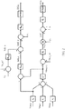
- Fig. 2 is a control diagram illustrating the calculation process to obtain the driving signal DS1a and the driving signal DS2a according to some embodiments of the present disclosure.
- a bus voltage average value Vbusavg is calculated by the control circuit 160 according to the intermediate bus voltages Vbusa, Vbusb, and Vbusc of the power modules Ma, Mb and Mc. Specifically, the intermediate bus voltages Vbusa, Vbusb, and Vbusc are multiplied by a bus voltage sensing gain Kv respectively, and then the mean value is calculated to obtain the bus voltage average value Vbusavg.
- the bus average voltage calculation changes correspondingly. Instead of dividing the total sum by three, the sum of the intermediate bus voltages from the healthy phases is divided by two.
- the bus voltage average value Vbusavg is calculated by the control circuit 160 according to the intermediate bus voltages Vbusb and Vbusc, of the power modules corresponding to remaining input phases (e.g., the power modules Mb, Mc).
- the driving signals DS1a, DS1b, DS1c and the driving signals DS2a, DS2b, DS2c are generated according to the bus voltage average value Vbusavg.
- the driving signal DS1a for the corresponding power module Ma is generated according to the bus voltage average value Vbusavg, the phase input voltage Va of the power module Ma, a phase input current Ia of the power module Ma, and a bus voltage reference value Vbusref, in which the bus voltage reference value Vbusref denotes a target value for the intermediate bus voltage Vbusa.
- the control circuit 160 is configured to calculate a difference between the bus voltage reference value Vbusref and the bus voltage average value Vbusavg.
- control circuit 160 is configured to amplify the difference between the bus voltage reference value Vbusref and the bus voltage average value Vbusavg by an error amplifier gain Gv to obtain an error amplification signal V EAa .
- control circuit 160 is configured to calculate an input current reference value Iaref based on the error amplification signal V EAa and the phase input voltage Va accordingly.
- the input current reference value laref denotes a target value for the phase input current Ia.
- control circuit 160 is configured to generate the driving signal DS1a according to a difference between the input current reference value laref and the phase input current Ia. Specifically, the control circuit 160 is configured to amplify the difference between the input current reference value laref and the actual phase input current Ia by a current gain Gi to obtain a current error amplification signal, and then the driving signal DS1a is generated with pulse width modulation (PWM) according to the current error amplification signal.
- PWM pulse width modulation
- the voltage of the artificial neutral point Ny with respect to the voltage of the actual neutral point N0 of the grid may be denoted by the following equation: V y 0 ⁇ Y a + V ao + Y b V bo + Y o Vco Y a + Y b + Y c
- Ya, Yb, Yc respectively denote the input admittances of the power supply 100 for each phase.
- the voltage of the artificial neutral point Ny is balanced, and the following equation is satisfied.
- V yo V ao + V bo + V co 3
- the same input admittances Ya, Yb, Yc are presented for each phase. Since the input admittance is proportional to the error amplification signal, the control circuit 160 is configured to ensure the error amplification signals V EAa , V EAb , V EAc are the same.
- the error amplifier gain Gv for all power modules Ma, Mb, Mc are the same in order to obtain the same error amplification signals V EAa , V EAb , V EAc for power modules Ma, Mb, Mc, in which the condition may be achieved by digital implementation.
- the intermediate bus voltages Vbusa, Vbusb, Vbusc are averaged before processing it through the error amplifiers for each phase, and the voltage of the artificial neutral point Ny may be properly controlled and balanced against the grid actual neutral point N0.
- control circuit 160 is configured to output the driving signals DS2a, DS2b, DS2c to control the operation of the DC-DC converter 140a, 140b, 140c, so as to keep the intermediate bus voltages Vbusa, Vbusb, Vbusc at proper level.
- the driving signals DS2a, DS2b, DS2c are also generated according to the bus voltage average value Vbusavg.
- the driving signal DS2a for the corresponding power module Ma is generated according to the bus voltage average value Vbusavg, the DC supply voltage Vo, a DC supply voltage reference value Vo_ref, an output current loa of the power module Ma, and the intermediate voltage Vbusa of the power module Ma.
- the control circuit 160 is configured to calculate a difference between the intermediate bus voltage Vbusa of the corresponding power module Ma and the bus voltage average value Vbusavg.
- control circuit 160 is configured to amplify the difference by a feed-forward gain Gff in order to obtain a feed-forward current adjustment signal Iadj_a.
- control circuit 160 is configured to accordingly sum up the feed-forward current adjustment signal Iadj_a and an output current reference value Iodc_a of the corresponding power module Ma to calculate an adjusted output current reference value Ioref_a.
- control circuit 160 is configured to generate the driving signal DS2a according to a difference between the adjusted output current reference value Ioref_a and the output current loa of the power module Ma. Specifically, the control circuit 160 is configured to amplify the difference between the adjusted output current reference value Ioref_a and the output current loa by a current gain Gidc to obtain a current error amplification signal, and then the driving signal DS2a is generated with pulse width modulation (PWM) according to the current error amplification signal.
- PWM pulse width modulation
- the control circuit 160 is configured to calculate the output current reference value Iodc_a base on a difference between the DC supply voltage reference value Vo_ref and the DC supply voltage Vo.
- the output current reference value Iodc_a is generated by multiplying the difference between the DC supply voltage reference value Vo_ref and the DC supply voltage Vo by an error amplifier gain Gvdc.
- the current reference for dc output current loop control of each module is adjusted, and the DC supply voltage Vo and the output current loa are respectively converge to the proper reference values. Accordingly, the intermediate bus voltage Vbusa of the corresponding power module Ma also converges to the average reference.
- Fig.3 is a diagram illustrating the power supply 100 according to some other embodiments of the present disclosure. Similar to the embodiment of Fig. 1 , the power supply 100 shown in Fig. 3 is also used in a three-phase power system, and configured to receive a three-phase input power, and correspondingly output a DC supply voltage Vo.
- each of the power modules Ma, Mb, Mc includes a plurality of power supply units PSU1a, PSU2a ⁇ PSUna, PSU1b, PSU2b ⁇ PSUnb, and PSU1c, PSU2c ⁇ PSUnc.
- Each of the power supply units PSU1a, PSU2a ⁇ PSUna includes an AC-DC converter 120a and a DC-DC converter 140a.
- the AC-DC converter 120a of the supply unit PSU1a is configured to convert the corresponding phase input voltage V1a of the power supply units PSU1a into the intermediate bus voltage Vbus1a.
- the DC-DC converter 140a of the supply unit PSU1a is configured to output the DC supply voltage Vo according to the intermediate bus voltage Vbus1a.
- the AC-DC converters 120a of the supply units PSU2a-PSUna are respectively configured to convert the corresponding phase input voltages V2a ⁇ Vna of the power supply units PSU2a ⁇ PSUna into the intermediate bus voltages Vbus2a ⁇ Vbusna.
- the DC-DC converters 140a of the supply units PSU2a ⁇ PSUna are configured to output the DC supply voltage Vo according to the intermediate bus voltage Vbus2a ⁇ Vbusna.
- the control circuit 160 is electrically coupled to the power supply units PSU1a, PSU2a ⁇ PSUna, PSU1b, PSU2b ⁇ PSUnb, and PSU1c, PSU2c ⁇ PSUnc. and configured to output corresponding driving signals to control the AC-DC converters 120a and the DC-DC converters 140a in the power supply units PSU1a, PSU2a ⁇ PSUna, PSU1b, PSU2b ⁇ PSUnb, and PSU1c, PSU2c ⁇ PSUnc.
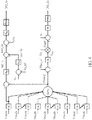
- Fig. 4 is a control diagram illustrating the calculation process to obtain the driving signal DS1_1a and the driving signal DS2_1a according to some embodiments of the present disclosure.
- the driving signal DS1_1a is configured to control and drive the AC-DC converters 120a in the power supply units PSU1a.
- the driving signal DS2_1a is configured to control and drive the DC-DC converters 140a in the power supply units PSU1a.
- the bus voltage average value Vbusavg is calculated by the control circuit 160 according to the intermediate bus voltages Vbus1a ⁇ Vbusna, Vbus1b ⁇ Vbusnb, and Vbus1c ⁇ Vbusnc, of the power supply units PSU1a ⁇ PSUna, PSU1b ⁇ PSUnb, and PSU1c ⁇ PSUnc, and the driving signal driving signal DS1_1a for the power supply unit PSU1a is generated according to the bus voltage average value Vbusavg.
- the driving signal DS1_1a for the power supply unit PSU1a is generated according to the bus voltage average value Vbusavg, the input voltage V1a of the power supply unit PSU1a, the input current Ia of the power supply unit PSU1a, and the bus voltage reference value Vbusref.
- the control circuit 160 is configured to calculate a difference between the bus voltage reference value Vbusref and the bus voltage average value Vbusavg, and amplify the difference by an error amplifier gain Gv to obtain the error amplification signal V EA1a , and accordingly calculate the input current reference value I1aref based on the error amplification signal V EA1a and the input voltage V1a of the power supply unit PSU1a.
- control circuit 160 is configured to generate the driving signal DS1_1a according to a difference between the input current reference value l1aref and the input current Ia of the power supply unit PSU1a.
- the driving signal DS2_1a for the power supply unit PSU1a is also generated according to the bus voltage average value Vbusavg.
- the driving signal DS2_1a for the corresponding power supply unit PSU1a is generated according to the bus voltage average value Vbusavg, the DC supply voltage Vo, the DC supply voltage reference value Vo_ref, the output current loa of the power supply unit PSU1a, and the intermediate voltage Vbus1a of the power supply unit PSU1a.
- control circuit 160 is configured to calculate a difference between the intermediate bus voltage Vbus1a of the corresponding power supply unit PSU1a and the bus voltage average value Vbusavg, and amplify the difference by a feed-forward gain Gff to obtain the feed-forward current adjustment signal Iadj_1a, and accordingly sum up the feed-forward current adjustment signal Iadj_1a and the output current reference value Iodc_1a of the corresponding power supply unit PSU1a to calculate the adjusted output current reference value Ioref_1a, so as to generate the driving signal DS2_1a according to the difference between the adjusted output current reference value Ioref_1a and the output current Io1a of the power supply unit PSU1a.
- control circuit 160 is configured to calculate the output current reference value Iodc_1a base on a difference of the DC supply voltage Vo and the DC supply voltage reference value Vo_ref.
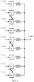
- Fig. 5 is a diagram illustrating the implementation of the calculation of the bus voltage average value Vbusavg.
- the intermediate bus voltages Vbus1a ⁇ Vbusna, Vbusb-Vbusnb, and Vbusc ⁇ Vbusnc may be coupled to a common node via corresponding resistor units.
- the voltage level of the common node may indicate the bus voltage average value Vbusavg.
- Fig. 6 is a control diagram illustrating the calculation process to obtain the driving signal DS1_1a and the driving signal DS2_1a according to some other embodiments of the present disclosure.
- control circuit 160 is further configured to calculate an error amplification signal average value V EAavg according to the error amplification signals V EA1a ⁇ V EAnc of the power supply units PSU1a ⁇ PSUna, PSU1b ⁇ PSUnb, and PSU1c ⁇ PSUnc.
- control circuit 160 is further configured to accordingly calculate the input current reference value I1aref based on the error amplification signal average value V EAavg and the input voltage V1a of the power supply unit PSU 1 a, so as to generate the driving signal DS1_1a according to the difference between the input current reference value I1aref and the input current Ia of the power supply unit PSU1a.
- the voltage of the artificial neutral point may be properly balanced, and the intermediate bus voltages in each power modules and power supply units may also be controlled.
Landscapes
- Engineering & Computer Science (AREA)
- Power Engineering (AREA)
- Inverter Devices (AREA)
- Dc-Dc Converters (AREA)
Abstract
Description
- The present disclosure relates to a power supply, and in particular, to a power supply used in a three-phase system.
- A three-phase power device may be implemented from single-phase modules. However, when an artificial floating neutral point is created by using a star configuration in the implementation of the three-phase power device, the instability of the artificial neutral point voltage may cause the three-phase AC power transmission at the grid-side unbalance.
- Therefore, an important area of research in the field involves ways in which to control the voltage of the artificial floating neutral point against the actual power grid neutral point.
- One aspect of the present disclosure is a power supply. The power supply includes a plurality of power modules and a control circuit. Input terminals of the power modules are electrically connected in star connection such that each power module receives a corresponding phase input voltage. Output terminals of the plurality of power modules are electrically connected in parallel, in which each power modules includes a first and a second converter. The first converter is configured to convert the corresponding phase input voltage into an intermediate bus voltage. The second converter is configured to output a DC supply voltage according to the intermediate bus voltage. The control circuit is electrically coupled to the power modules and configured to output first driving signals to control the first converters in the power modules, and configured to output second driving signals to control the second converters in the power modules. A bus voltage average value is calculated by the control circuit according to the intermediate bus voltages of the power modules, and the first driving signals and the second driving signals for the power modules are generated according to the bus voltage average value.
- Yet another aspect of the present disclosure is a power supply control method. The power supply control method includes detecting a plurality of intermediate bus voltages of a plurality of power modules of a power supply respectively; calculating, by a control circuit of the power supply, a bus voltage average value according to the intermediate bus voltages of the power modules; outputting, by the control circuit, a plurality of first driving signals according to the bus voltage average value to respectively control a plurality of first converters in the power modules; and outputting, by the control circuit, a plurality of second driving signals according to the bus voltage average value to respectively control a plurality of second converters in the power modules.
- It is to be understood that both the foregoing general description and the following detailed description are by examples, and are intended to provide further explanation of the disclosure as claimed.
- The disclosure can be more fully understood by reading the following detailed description of the embodiments, with reference made to the accompanying drawings as follows:
-
Fig.1 is a diagram illustrating a power supply according to some embodiments of the present disclosure. -
Fig. 2 is a control diagram illustrating the calculation process to obtain the driving signal and the driving signal according to some embodiments of the present disclosure. -
Fig.3 is a diagram illustrating the power supply according to some other embodiments of the present disclosure. -
Fig. 4 is a control diagram illustrating the calculation process to obtain the driving signal and the driving signal according to some embodiments of the present disclosure. -
Fig. 5 is a diagram illustrating the implementation of the calculation of the bus voltage average value. -
Fig. 6 is a control diagram illustrating the calculation process to obtain the driving signal and the driving signal according to some other embodiments of the present disclosure. - Reference will now be made in detail to embodiments of the present disclosure, examples of which are described herein and illustrated in the accompanying drawings. While the disclosure will be described in conjunction with embodiments, it will be understood that they are not intended to limit the disclosure to these embodiments. It is noted that, in accordance with the standard practice in the industry, the drawings are only used for understanding and are not drawn to scale. Hence, the drawings are not meant to limit the actual embodiments of the present disclosure. In fact, the dimensions of the various features may be arbitrarily increased or reduced for clarity of discussion. Wherever possible, the same reference numbers are used in the drawings and the description to refer to the same or like parts for better understanding.
- The terms used in this specification and claims, unless otherwise stated, generally have their ordinary meanings in the art, within the context of the disclosure, and in the specific context where each term is used. Certain terms that are used to describe the disclosure are discussed below, or elsewhere in the specification, to provide additional guidance to the practitioner skilled in the art regarding the description of the disclosure.
- The terms "about" and "approximately" in the disclosure are used as equivalents. Any numerals used in this disclosure with or without "about," "approximately," etc. are meant to cover any normal fluctuations appreciated by one of ordinary skill in the relevant art. In certain embodiments, the term "approximately" or "about" refers to a range of values that fall within 20%, 10%, 5%, or less in either direction (greater or less than) of the stated reference value unless otherwise stated or otherwise evident from the context.
- In the following description and in the claims, the terms "include" and "comprise" are used in an open-ended fashion, and thus should be interpreted to mean "include, but not limited to." As used herein, the term "and/or" includes any and all combinations of one or more of the associated listed items.
- In this document, the term "coupled" may also be termed "electrically coupled," and the term "connected" may be termed "electrically connected." "Coupled" and "connected" may also be used to indicate that two or more elements cooperate or interact with each other. It will be understood that, although the terms "first," "second," etc., may be used herein to describe various elements, these elements should not be limited by these terms. These terms are used to distinguish one element from another. For example, a first element could be termed a second element, and, similarly, a second element could be termed a first element, without departing from the scope of the embodiments.
- Reference is made to
Fig. 1. Fig.1 is a diagram illustrating apower supply 100 according to some embodiments of the present disclosure. As shown inFig. 1 , thepower supply 100 is used in a three-phase power system, and configured to receive a three-phase input power, and correspondingly output a DC supply voltage Vo. - Specifically, the
power supply 100 includes three single-phase power modules Ma, Mb, and Mc and acontrol circuit 160. Input terminals of the power modules Ma, Mb, and Mc are electrically connected in star connection such that each of the power modules Ma, Mb, and Mc is configured to receive a corresponding phase input voltage Va, Vb, or Vc and a corresponding phase input current Ia, Ib, or Ic. Output terminals of the power modules Ma, Mb, and Mc are electrically connected in parallel. - As shown in the drawing, the star connection at the input side of the power modules Ma, Mb, and Mc creates the artificial neutral point Ny in the
power supply 100 which needs to be balanced against the actual neutral point N0 of the grid. By applying the configuration shown inFig. 1 , the single-phase power modules Ma, Mb, and Mc may now be used in thepower supply 100 for three-phase configuration. - In some embodiments, each of the power modules Ma, Mb, and Mc respectively includes an AC-
DC converter DC converter DC converters DC converters DC converters - The DC-
DC converters DC converters - The
control circuit 160 is electrically coupled to the power modules Ma, Mb, and Mc, and configured to output driving signals DS1a, DS1b, DS1c to control and drive the AC-DC converters DC converters - For better understanding of the present disclosure, the control method of the
power supply 100 to control the voltage level of the artificial neutral point Ny by providing proper driving signals DS1a, DS1b, DS1c and driving signals DS2a, DS2b, DS2c will be discussed in accompanied with drawings in the following paragraphs. - Reference is made to
Fig. 2. Fig. 2 is a control diagram illustrating the calculation process to obtain the driving signal DS1a and the driving signal DS2a according to some embodiments of the present disclosure. - As depicted in
Fig. 2 , a bus voltage average value Vbusavg is calculated by thecontrol circuit 160 according to the intermediate bus voltages Vbusa, Vbusb, and Vbusc of the power modules Ma, Mb and Mc. Specifically, the intermediate bus voltages Vbusa, Vbusb, and Vbusc are multiplied by a bus voltage sensing gain Kv respectively, and then the mean value is calculated to obtain the bus voltage average value Vbusavg. In some embodiments, in the event that one of the input phases drops out, the bus average voltage calculation changes correspondingly. Instead of dividing the total sum by three, the sum of the intermediate bus voltages from the healthy phases is divided by two. Alternatively stated, in the event that an input phase (e.g., the phase corresponding to the power module Ma) drops out, the bus voltage average value Vbusavg is calculated by thecontrol circuit 160 according to the intermediate bus voltages Vbusb and Vbusc, of the power modules corresponding to remaining input phases (e.g., the power modules Mb, Mc). - In some embodiments, the driving signals DS1a, DS1b, DS1c and the driving signals DS2a, DS2b, DS2c are generated according to the bus voltage average value Vbusavg.
- For example, the driving signal DS1a for the corresponding power module Ma is generated according to the bus voltage average value Vbusavg, the phase input voltage Va of the power module Ma, a phase input current Ia of the power module Ma, and a bus voltage reference value Vbusref, in which the bus voltage reference value Vbusref denotes a target value for the intermediate bus voltage Vbusa. As shown in
Fig. 2 , thecontrol circuit 160 is configured to calculate a difference between the bus voltage reference value Vbusref and the bus voltage average value Vbusavg. - Next, the
control circuit 160 is configured to amplify the difference between the bus voltage reference value Vbusref and the bus voltage average value Vbusavg by an error amplifier gain Gv to obtain an error amplification signal VEAa. - Next, the
control circuit 160 is configured to calculate an input current reference value Iaref based on the error amplification signal VEAa and the phase input voltage Va accordingly. The input current reference value laref denotes a target value for the phase input current Ia. - Next, the
control circuit 160 is configured to generate the driving signal DS1a according to a difference between the input current reference value laref and the phase input current Ia. Specifically, thecontrol circuit 160 is configured to amplify the difference between the input current reference value laref and the actual phase input current Ia by a current gain Gi to obtain a current error amplification signal, and then the driving signal DS1a is generated with pulse width modulation (PWM) according to the current error amplification signal. - For the three-phase system, the voltage of the artificial neutral point Ny with respect to the voltage of the actual neutral point N0 of the grid may be denoted by the following equation:
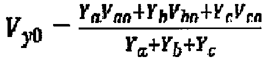
- In the above equation, Ya, Yb, Yc respectively denote the input admittances of the
power supply 100 for each phase. When the input admittances Ya, Yb, Yc for each phase are the same, the voltage of the artificial neutral point Ny is balanced, and the following equation is satisfied.
- Alternatively stated, in order to balance the voltage of the artificial neutral point Ny, the same input admittances Ya, Yb, Yc are presented for each phase. Since the input admittance is proportional to the error amplification signal, the
control circuit 160 is configured to ensure the error amplification signals VEAa, VEAb, VEAc are the same. - Therefore, in the control method shown in
Fig. 2 , the error amplifier gain Gv for all power modules Ma, Mb, Mc, are the same in order to obtain the same error amplification signals VEAa, VEAb, VEAc for power modules Ma, Mb, Mc, in which the condition may be achieved by digital implementation. Thus, by applying the control method stated above, the intermediate bus voltages Vbusa, Vbusb, Vbusc are averaged before processing it through the error amplifiers for each phase, and the voltage of the artificial neutral point Ny may be properly controlled and balanced against the grid actual neutral point N0. - Although the average dc link voltage is controlled to a given reference, in order to further control each of the intermediate bus voltages Vbusa, Vbusb, Vbusc, a feed-forward control of the intermediate bus voltages Vbusa, Vbusb, Vbusc of the power modules Ma, Mb, Mc is applied.
- Specifically, the
control circuit 160 is configured to output the driving signals DS2a, DS2b, DS2c to control the operation of the DC-DC converter - As mentioned above, the driving signals DS2a, DS2b, DS2c are also generated according to the bus voltage average value Vbusavg. For example, the driving signal DS2a for the corresponding power module Ma is generated according to the bus voltage average value Vbusavg, the DC supply voltage Vo, a DC supply voltage reference value Vo_ref, an output current loa of the power module Ma, and the intermediate voltage Vbusa of the power module Ma. As shown in
Fig. 2 , thecontrol circuit 160 is configured to calculate a difference between the intermediate bus voltage Vbusa of the corresponding power module Ma and the bus voltage average value Vbusavg. - Next, the
control circuit 160 is configured to amplify the difference by a feed-forward gain Gff in order to obtain a feed-forward current adjustment signal Iadj_a. - Next, the
control circuit 160 is configured to accordingly sum up the feed-forward current adjustment signal Iadj_a and an output current reference value Iodc_a of the corresponding power module Ma to calculate an adjusted output current reference value Ioref_a. - Next, the
control circuit 160 is configured to generate the driving signal DS2a according to a difference between the adjusted output current reference value Ioref_a and the output current loa of the power module Ma. Specifically, thecontrol circuit 160 is configured to amplify the difference between the adjusted output current reference value Ioref_a and the output current loa by a current gain Gidc to obtain a current error amplification signal, and then the driving signal DS2a is generated with pulse width modulation (PWM) according to the current error amplification signal. - As shown in
Fig. 2 , in some embodiments, thecontrol circuit 160 is configured to calculate the output current reference value Iodc_a base on a difference between the DC supply voltage reference value Vo_ref and the DC supply voltage Vo. The output current reference value Iodc_a is generated by multiplying the difference between the DC supply voltage reference value Vo_ref and the DC supply voltage Vo by an error amplifier gain Gvdc. - Since the feed-forward control of the intermediate bus voltage Vbusa is applied, the current reference for dc output current loop control of each module is adjusted, and the DC supply voltage Vo and the output current loa are respectively converge to the proper reference values. Accordingly, the intermediate bus voltage Vbusa of the corresponding power module Ma also converges to the average reference.
- It is noted that although the calculation process of the driving signals DS1a and DS2a for driving the power module Ma is mainly discussed above, the calculation process for the driving signals DS1b, DS1c and DS2b, DS2c for driving the power modules Mb, Mc is similar thereto and thus further explanations are omitted herein for the sake of brevity.
- Reference is made to
Fig. 3. Fig.3 is a diagram illustrating thepower supply 100 according to some other embodiments of the present disclosure. Similar to the embodiment ofFig. 1 , thepower supply 100 shown inFig. 3 is also used in a three-phase power system, and configured to receive a three-phase input power, and correspondingly output a DC supply voltage Vo. - Compared to the embodiment of
Fig. 1 , in the present embodiment, each of the power modules Ma, Mb, Mc includes a plurality of power supply units PSU1a, PSU2a∼PSUna, PSU1b, PSU2b∼PSUnb, and PSU1c, PSU2c∼PSUnc. - For example, input terminals of the power supply units PSU1a, PSU2a∼PSUna in the same power module Ma are electrically coupled in series, output terminals of the power supply units PSU1a, PSU2a∼PSUna in the same power module Ma are electrically coupled in parallel. Each of the power supply units PSU1a, PSU2a∼PSUna includes an AC-
DC converter 120a and a DC-DC converter 140a. - Similar to the embodiments mentioned above, the AC-
DC converter 120a of the supply unit PSU1a is configured to convert the corresponding phase input voltage V1a of the power supply units PSU1a into the intermediate bus voltage Vbus1a. The DC-DC converter 140a of the supply unit PSU1a is configured to output the DC supply voltage Vo according to the intermediate bus voltage Vbus1a. Similarly, the AC-DC converters 120a of the supply units PSU2a-PSUna are respectively configured to convert the corresponding phase input voltages V2a∼Vna of the power supply units PSU2a∼PSUna into the intermediate bus voltages Vbus2a∼Vbusna. The DC-DC converters 140a of the supply units PSU2a∼PSUna are configured to output the DC supply voltage Vo according to the intermediate bus voltage Vbus2a∼Vbusna. - The
control circuit 160 is electrically coupled to the power supply units PSU1a, PSU2a∼PSUna, PSU1b, PSU2b∼PSUnb, and PSU1c, PSU2c∼PSUnc. and configured to output corresponding driving signals to control the AC-DC converters 120a and the DC-DC converters 140a in the power supply units PSU1a, PSU2a∼PSUna, PSU1b, PSU2b∼PSUnb, and PSU1c, PSU2c∼PSUnc. - Reference is made to
Fig. 4. Fig. 4 is a control diagram illustrating the calculation process to obtain the driving signal DS1_1a and the driving signal DS2_1a according to some embodiments of the present disclosure. - The driving signal DS1_1a is configured to control and drive the AC-
DC converters 120a in the power supply units PSU1a. The driving signal DS2_1a is configured to control and drive the DC-DC converters 140a in the power supply units PSU1a. Similar to the above embodiments, the bus voltage average value Vbusavg is calculated by thecontrol circuit 160 according to the intermediate bus voltages Vbus1a∼Vbusna, Vbus1b∼Vbusnb, and Vbus1c∼Vbusnc, of the power supply units PSU1a∼PSUna, PSU1b∼PSUnb, and PSU1c∼PSUnc, and the driving signal driving signal DS1_1a for the power supply unit PSU1a is generated according to the bus voltage average value Vbusavg. - For example, the driving signal DS1_1a for the power supply unit PSU1a is generated according to the bus voltage average value Vbusavg, the input voltage V1a of the power supply unit PSU1a, the input current Ia of the power supply unit PSU1a, and the bus voltage reference value Vbusref.
- The
control circuit 160 is configured to calculate a difference between the bus voltage reference value Vbusref and the bus voltage average value Vbusavg, and amplify the difference by an error amplifier gain Gv to obtain the error amplification signal VEA1a, and accordingly calculate the input current reference value I1aref based on the error amplification signal VEA1a and the input voltage V1a of the power supply unit PSU1a. - Next, the
control circuit 160 is configured to generate the driving signal DS1_1a according to a difference between the input current reference value l1aref and the input current Ia of the power supply unit PSU1a. - In addition, the driving signal DS2_1a for the power supply unit PSU1a is also generated according to the bus voltage average value Vbusavg.
- For example, the driving signal DS2_1a for the corresponding power supply unit PSU1a is generated according to the bus voltage average value Vbusavg, the DC supply voltage Vo, the DC supply voltage reference value Vo_ref, the output current loa of the power supply unit PSU1a, and the intermediate voltage Vbus1a of the power supply unit PSU1a.
- Specifically, the
control circuit 160 is configured to calculate a difference between the intermediate bus voltage Vbus1a of the corresponding power supply unit PSU1a and the bus voltage average value Vbusavg, and amplify the difference by a feed-forward gain Gff to obtain the feed-forward current adjustment signal Iadj_1a, and accordingly sum up the feed-forward current adjustment signal Iadj_1a and the output current reference value Iodc_1a of the corresponding power supply unit PSU1a to calculate the adjusted output current reference value Ioref_1a, so as to generate the driving signal DS2_1a according to the difference between the adjusted output current reference value Ioref_1a and the output current Io1a of the power supply unit PSU1a. - Similar to the embodiments mentioned above, the
control circuit 160 is configured to calculate the output current reference value Iodc_1a base on a difference of the DC supply voltage Vo and the DC supply voltage reference value Vo_ref. - Reference is made to
Fig. 5. Fig. 5 is a diagram illustrating the implementation of the calculation of the bus voltage average value Vbusavg. As depicted inFig. 5 , after multiplied by bus voltage sensing gain Kv respectively, the intermediate bus voltages Vbus1a∼Vbusna, Vbusb-Vbusnb, and Vbusc∼Vbusnc may be coupled to a common node via corresponding resistor units. Thus, the voltage level of the common node may indicate the bus voltage average value Vbusavg. - Reference is made to
Fig. 6. Fig. 6 is a control diagram illustrating the calculation process to obtain the driving signal DS1_1a and the driving signal DS2_1a according to some other embodiments of the present disclosure. - Compared to the embodiment of
Fig. 4 , in the present embodiment, thecontrol circuit 160 is further configured to calculate an error amplification signal average value VEAavg according to the error amplification signals VEA1a∼VEAnc of the power supply units PSU1a∼PSUna, PSU1b∼PSUnb, and PSU1c∼PSUnc. - Next, the
control circuit 160 is further configured to accordingly calculate the input current reference value I1aref based on the error amplification signal average value VEAavg and the input voltage V1a of the power supply unit PSU 1 a, so as to generate the driving signal DS1_1a according to the difference between the input current reference value I1aref and the input current Ia of the power supply unit PSU1a. - Slight difference of the bus voltage reference values Vbusref or error amplifier gains Gv may present in different power supply units and lead to different error amplification signals VEA1a∼VEAnc, causing the different input admittances of the various PSUs and instability of the voltage of the artificial neutral point Ny in analog implementation. Therefore, by including a mismatch compensation for parameter differences and calculating the error amplification signal average value VEAavg to generate the driving signal DS1_1a may overcome the aforementioned issues resulted from the components' mismatch in analog implementation.
- It is noted that although the calculation process of the driving signals DS1_1a and DS2_1a for driving the power supply unit PSU1a is mainly discussed above, the calculation process for the driving signals for driving other power supply units is similar thereto and thus further explanations are omitted herein for the sake of brevity.
- Those skilled in the art can immediately understand how to perform the operations and functions of the control method based on the
power supply 100 in the embodiments described above, and thus a further explanation is omitted herein for the sake of brevity. - In summary, in the present disclosure, by averaging the voltage outputted by the AC-DC converters in each power modules and power supply units before processing it through the error amplifiers for each phase, the voltage of the artificial neutral point may be properly balanced, and the intermediate bus voltages in each power modules and power supply units may also be controlled.
Claims (15)
- A power supply (100), characterized by comprising:a plurality of power modules (Ma, Mb, Mc), input terminals of the plurality of power modules being electrically connected in star connection such that each power module receives a corresponding phase input voltage (Va, Vb, Vc), output terminals of the plurality of power modules being electrically connected in parallel, wherein each of the plurality of power modules comprises:a first converter (120a, 120b, 120c) configured to convert the corresponding phase input voltage into an intermediate bus voltage (Vbusa, Vbusb, Vbusc); anda second converter (140a, 140b, 140c) configured to output a DC supply voltage (Vo) according to the intermediate bus voltage; anda control circuit (160) electrically coupled to the plurality of power modules and configured to output a plurality of first driving signals (DS1a, DS1b, DS1c) to control the first converters in the plurality of power modules, and configured to output a plurality of second driving signals (DS2a, DS2b, DS2c) to control the second converters in the plurality of power modules;wherein a bus voltage average value (Vbusavg) is calculated by the control circuit according to the intermediate bus voltages of the plurality of power modules, and the first driving signals and the second driving signals for the plurality of power modules are generated according to the bus voltage average value.
- The power supply of claim 1, wherein the first driving signal for the corresponding power module is generated according to the bus voltage average value, the phase input voltage of the power module, a phase input current (Ia, Ib, Ic) of the power module, and a bus voltage reference value (Vbusref).
- The power supply of claim 2, wherein the control circuit is configured to calculate a difference between the bus voltage reference value and the bus voltage average value and amplify the difference to obtain an error amplification signal (VEAa, VEAb, VEAC), and accordingly calculate an input current reference value (Iaref) based on the error amplification signal and the phase input voltage.
- The power supply of claim 3, wherein the control circuit is further configured to generate the first driving signal according to a difference between the input current reference value and the phase input current.
- The power supply of claim 1, wherein the second driving signal for the corresponding power module is generated according to the bus voltage average value, the DC supply voltage, a DC supply voltage reference value (Vo_ref), an output current of the power module, and the intermediate voltage of the power module (loa).
- The power supply of claim 5, wherein the control circuit is configured to calculate a difference between the intermediate bus voltage of the corresponding power module and the bus voltage average value, and amplify the difference to obtain a feed-forward current adjustment signal (Iadj_a), and accordingly sum up the feed-forward current adjustment signal and a first output current reference value (Iodc_a) of the corresponding power module to calculate a second output current reference value (Ioref_a), so as to generate the second driving signal according to a difference between the second output current reference value and the output current of the power module.
- The power supply of claim 6, wherein the control circuit is configured to calculate the first output current reference value base on a difference of the DC supply voltage and the DC supply voltage reference value.
- The power supply of claim 1, wherein in the event that an input phase drops out, the bus voltage average value is calculated by the control circuit according to the intermediate bus voltages of the power modules corresponding to remaining input phases.
- The power supply of claim 1, wherein each of the power modules comprises a plurality of power supply units (PSU1a, PSU2a∼PSUna, PSU1b, PSU2b∼PSUnb, PSU1c, PSU2c∼PSUnc), wherein input terminals of the power supply units in the same power module are electrically coupled in series, and output terminals of the power supply units in the same power module are electrically coupled in parallel, and each of the power supply units comprises the corresponding first converter and the corresponding second converter, and the control circuit is further electrically coupled to the plurality of power supply units and configured to output the plurality of first driving signals to control the first converters in the plurality of power supply units;
wherein the bus voltage average value is calculated by the control circuit according to the intermediate bus voltages of the plurality of power supply units, and the first driving signals for the plurality of power supply units are generated according to the bus voltage average value. - The power supply of claim 9, wherein the first driving signal for the corresponding power supply unit is generated according to the bus voltage average value, an input voltage (V1a∼Vna) of the power supply unit, an input current (Ia) of the power supply unit, and a bus voltage reference value (Vbusref), the control circuit is configured to calculate a difference between the bus voltage reference value and the bus voltage average value, amplify the difference to obtain an error amplification signal (VEA1a), and accordingly calculate an input current reference value (I1aref) based on the error amplification signal and the input voltage of the power supply unit, so as to generate the first driving signal according to a difference between the input current reference value and the input current of the power supply unit, and the control circuit is further configured to calculate an error amplification signal average value (VEAavg) according to the error amplification signals of the power supply units, and accordingly calculate the input current reference value based on the error amplification signal average value and the input voltage of the power supply unit, so as to generate the first driving signal according to a difference between the input current reference value and the input current of the power supply unit.
- A power supply control method, characterized by comprising:detecting a plurality of intermediate bus voltages (Vbusa, Vbusb, Vbusc) of a plurality of power modules (Ma, Mb, Mc) of a power supply (100) respectively;calculating, by a control circuit (160) of the power supply, a bus voltage average value (Vbusavg) according to the intermediate bus voltages of the plurality of power modules;outputting, by the control circuit, a plurality of first driving signals (DS1a, DS1 b, DS1c) according to the bus voltage average value to respectively control a plurality of first converters (120a, 120b, 120c) in the plurality of power modules; andoutputting, by the control circuit, a plurality of second driving signals DS2a, DS2b, DS2c according to the bus voltage average value to respectively control a plurality of second converters (140a, 140b, 140c) in the plurality of power modules.
- The power supply control method of claim 11, further comprising:generating, by the control circuit, the first driving signal for the corresponding power module according to the bus voltage average value, a phase input voltage (Va) of the power module, a phase input current (Ia) of the power module, and a bus voltage reference value (Vbusref).
- The power supply control method of claim 12, wherein generating the first driving signal for the corresponding power module comprises:calculating a difference between the bus voltage reference value and the bus voltage average value;amplifying the difference between the bus voltage reference value and the bus voltage average value to obtain an error amplification signal (VEAa);calculating an input current reference value (Iaref) based on the error amplification signal and the phase input voltage accordingly; andgenerating the first driving signal according to a difference between the input current reference value and the phase input current.
- The power supply control method of claim 11, further comprising:generating the second driving signal for the corresponding power module according to the bus voltage average value, a DC supply voltage (Vo), a DC supply voltage reference value (Vo_ref), an output current (Ioa) of the power module, and the intermediate voltage of the power module.
- The power supply control method of claim 14, wherein generating the second driving signal for the corresponding power module comprises:calculating a difference between the intermediate bus voltage of the corresponding power module and the bus voltage average value;amplifying the difference between the intermediate bus voltage of the corresponding power module and the bus voltage average value to obtain a feed-forward current adjustment signal (Iadj_a);calculating a first output current reference value (Iodc_a) base on a difference between the DC supply voltage reference value and the DC supply voltage;summing up the feed-forward current adjustment signal and the first output current reference value of the corresponding power module to calculate a second output current reference value (Ioref_a) accordingly; andgenerating the second driving signal according to a difference between the second output current reference value and the output current of the power module.
Applications Claiming Priority (1)
| Application Number | Priority Date | Filing Date | Title |
|---|---|---|---|
| US15/658,894 US10153710B1 (en) | 2017-07-25 | 2017-07-25 | Power supply and control method thereof |
Publications (2)
| Publication Number | Publication Date |
|---|---|
| EP3435533A1 true EP3435533A1 (en) | 2019-01-30 |
| EP3435533B1 EP3435533B1 (en) | 2021-05-05 |
Family
ID=59745835
Family Applications (1)
| Application Number | Title | Priority Date | Filing Date |
|---|---|---|---|
| EP17188859.7A Active EP3435533B1 (en) | 2017-07-25 | 2017-08-31 | Power supply and control method thereof |
Country Status (3)
| Country | Link |
|---|---|
| US (1) | US10153710B1 (en) |
| EP (1) | EP3435533B1 (en) |
| CN (1) | CN109302089B (en) |
Cited By (2)
| Publication number | Priority date | Publication date | Assignee | Title |
|---|---|---|---|---|
| EP4231516A1 (en) * | 2022-02-22 | 2023-08-23 | Abb Schweiz Ag | Damping higher order harmonics in average dc link voltages |
| DE102023105145A1 (en) | 2023-03-02 | 2024-09-05 | Brusa Elektronik Ag | MULTI-PHASE INVERTER AND PHASE LOAD BALANCING METHODS |
Families Citing this family (11)
| Publication number | Priority date | Publication date | Assignee | Title |
|---|---|---|---|---|
| CN107104443B (en) * | 2017-06-21 | 2023-05-23 | 西南交通大学 | A power electronic transformer |
| CN112928898B (en) * | 2019-12-06 | 2026-02-17 | 中兴通讯股份有限公司 | BUS voltage equalization regulation method and power converter |
| CN111313724A (en) * | 2020-04-02 | 2020-06-19 | 西安科技大学 | Power module series-parallel connection management system |
| KR102942698B1 (en) * | 2020-04-07 | 2026-03-23 | 엘지이노텍 주식회사 | Load sharing controller |
| JP7102473B2 (en) * | 2020-08-19 | 2022-07-19 | 株式会社三社電機製作所 | Parallel operation power supply |
| KR20220037280A (en) * | 2020-09-17 | 2022-03-24 | 삼성전자주식회사 | Power supply method and electronic device usint the same |
| CN116783817A (en) * | 2021-01-22 | 2023-09-19 | 华为数字能源技术有限公司 | A detection method and related devices |
| CN115347805B (en) * | 2021-05-12 | 2026-04-03 | 台达电子企业管理(上海)有限公司 | Power supply equipment and its control methods, three-phase power supply system and its control methods |
| CN113300583B (en) * | 2021-05-24 | 2022-08-16 | 深圳市高德威技术有限公司 | Automatic current-sharing step ratio control method for communication power supply module |
| CN115037139A (en) * | 2022-06-22 | 2022-09-09 | 南京博兰得电子科技有限公司 | Redundant hot backup power supply and current sharing control method thereof |
| US12549015B2 (en) * | 2022-12-29 | 2026-02-10 | Rivian Ip Holdings, Llc | Sensorless current sharing for power converters |
Citations (3)
| Publication number | Priority date | Publication date | Assignee | Title |
|---|---|---|---|---|
| US20100124083A1 (en) * | 2008-11-17 | 2010-05-20 | Lockheed Martin Corporation | 3-phase power factor corrected ac to dc filtered switching power supply |
| WO2015076776A1 (en) * | 2013-11-19 | 2015-05-28 | Richards Corporation | Multi-phase active power factor correction system |
| EP2999109A1 (en) * | 2014-09-17 | 2016-03-23 | Delta Electronics, Inc. | Power supply and method of supplying power |
Family Cites Families (12)
| Publication number | Priority date | Publication date | Assignee | Title |
|---|---|---|---|---|
| TW395627U (en) | 1998-08-10 | 2000-06-21 | Luo You Gang | Switching rectifier for three-phase three-wire Y-connection power source |
| JP4699659B2 (en) * | 2000-12-25 | 2011-06-15 | 新電元工業株式会社 | Multiphase rectifier |
| US7005835B2 (en) | 2002-06-28 | 2006-02-28 | Microsemi Corp. | Method and apparatus for load sharing in a multiphase switching power converter |
| CN101494414A (en) * | 2008-01-22 | 2009-07-29 | 台达电子工业股份有限公司 | Distributed power supply structure |
| JP5304192B2 (en) * | 2008-03-28 | 2013-10-02 | ダイキン工業株式会社 | Power converter |
| KR101023336B1 (en) * | 2009-07-03 | 2011-03-18 | 삼성전기주식회사 | Load sharing device and parallel power supply with the same |
| US8553440B1 (en) * | 2010-09-24 | 2013-10-08 | James Nanut | Power conversion circuits |
| US9099935B2 (en) * | 2013-01-14 | 2015-08-04 | Yaskawa America, Inc. | Single-phase active front end rectifier system for use with three-phase variable frequency drives |
| CN103390995B (en) * | 2013-07-18 | 2015-09-30 | 矽力杰半导体技术(杭州)有限公司 | A kind of pfc circuit |
| US9621070B2 (en) * | 2014-09-17 | 2017-04-11 | Delta Electronics, Inc. | Power supply with multiple converters and averaged feedforward control |
| AU2015203405B2 (en) | 2015-06-19 | 2018-03-08 | Rectifier Technologies Pacific Pty Ltd | Control of a three phase AC-DC power converter comprising three single phase modules |
| GB201610369D0 (en) * | 2016-06-15 | 2016-07-27 | Rolls Royce Plc | Control of an electrical converter |
-
2017
- 2017-07-25 US US15/658,894 patent/US10153710B1/en active Active
- 2017-08-31 EP EP17188859.7A patent/EP3435533B1/en active Active
-
2018
- 2018-02-24 CN CN201810156112.4A patent/CN109302089B/en active Active
Patent Citations (3)
| Publication number | Priority date | Publication date | Assignee | Title |
|---|---|---|---|---|
| US20100124083A1 (en) * | 2008-11-17 | 2010-05-20 | Lockheed Martin Corporation | 3-phase power factor corrected ac to dc filtered switching power supply |
| WO2015076776A1 (en) * | 2013-11-19 | 2015-05-28 | Richards Corporation | Multi-phase active power factor correction system |
| EP2999109A1 (en) * | 2014-09-17 | 2016-03-23 | Delta Electronics, Inc. | Power supply and method of supplying power |
Cited By (4)
| Publication number | Priority date | Publication date | Assignee | Title |
|---|---|---|---|---|
| EP4231516A1 (en) * | 2022-02-22 | 2023-08-23 | Abb Schweiz Ag | Damping higher order harmonics in average dc link voltages |
| WO2023161066A1 (en) * | 2022-02-22 | 2023-08-31 | Abb Schweiz Ag | Damping higher order harmonics in average dc link voltages |
| DE102023105145A1 (en) | 2023-03-02 | 2024-09-05 | Brusa Elektronik Ag | MULTI-PHASE INVERTER AND PHASE LOAD BALANCING METHODS |
| WO2024180187A1 (en) | 2023-03-02 | 2024-09-06 | Brusa Elektronik Ag | Multiphase converter and method for compensating for phase loads |
Also Published As
| Publication number | Publication date |
|---|---|
| CN109302089B (en) | 2021-03-09 |
| EP3435533B1 (en) | 2021-05-05 |
| CN109302089A (en) | 2019-02-01 |
| US10153710B1 (en) | 2018-12-11 |
Similar Documents
| Publication | Publication Date | Title |
|---|---|---|
| EP3435533B1 (en) | Power supply and control method thereof | |
| US10205402B2 (en) | Power conversion device for converting power between a DC circuit and an AC circuit by performing a non-linear operation | |
| US10637343B2 (en) | Power conversion device for reliable control of circulating current | |
| US11228247B2 (en) | Parallel power supply device | |
| US9444323B2 (en) | Power conversion system having a harmonic distortion limiter | |
| US10560036B2 (en) | Power conversion device for reliable control of circulating current while maintaining voltage of a cell | |
| CN104300791B (en) | Switching power supply apparatus | |
| US8947148B2 (en) | Hybrid analog/digital point-of-load controller | |
| JP7018847B2 (en) | Switching power supply system and DC power supply system | |
| US10454374B2 (en) | Power supply | |
| AU2019204473A1 (en) | Neutral Connection Detection Method For 3/4 -Wire Active Filters | |
| EP3100347B1 (en) | System and method for detecting and correcting dc bus imbalances between parallel coupled ups systems sharing a common battery | |
| US20080151585A1 (en) | Converter Control Apparatus | |
| KR20220043388A (en) | Apparatus and method for controlling multi-phase interleaved voltage balancer | |
| US8963370B2 (en) | Load sharing apparatus | |
| US10581338B2 (en) | Power supply system | |
| WO2021236163A8 (en) | Method and apparatus for phase current balancing in a multi-phase dc-to-dc converter | |
| EP3370330A1 (en) | Switching power source device and droop characteristic correction method | |
| KR101625401B1 (en) | Converter module and converter system | |
| EP4693789A1 (en) | Dc/dc converter and power supply system | |
| JP3735646B2 (en) | AC / DC converter controller | |
| CN118677045A (en) | Vehicle battery output system and driving method thereof | |
| JP2003111491A (en) | Power converter | |
| JPS63217977A (en) | Inverter device |
Legal Events
| Date | Code | Title | Description |
|---|---|---|---|
| PUAI | Public reference made under article 153(3) epc to a published international application that has entered the european phase |
Free format text: ORIGINAL CODE: 0009012 |
|
| STAA | Information on the status of an ep patent application or granted ep patent |
Free format text: STATUS: REQUEST FOR EXAMINATION WAS MADE |
|
| 17P | Request for examination filed |
Effective date: 20180706 |
|
| AK | Designated contracting states |
Kind code of ref document: A1 Designated state(s): AL AT BE BG CH CY CZ DE DK EE ES FI FR GB GR HR HU IE IS IT LI LT LU LV MC MK MT NL NO PL PT RO RS SE SI SK SM TR |
|
| AX | Request for extension of the european patent |
Extension state: BA ME |
|
| GRAP | Despatch of communication of intention to grant a patent |
Free format text: ORIGINAL CODE: EPIDOSNIGR1 |
|
| STAA | Information on the status of an ep patent application or granted ep patent |
Free format text: STATUS: GRANT OF PATENT IS INTENDED |
|
| INTG | Intention to grant announced |
Effective date: 20210121 |
|
| GRAS | Grant fee paid |
Free format text: ORIGINAL CODE: EPIDOSNIGR3 |
|
| GRAA | (expected) grant |
Free format text: ORIGINAL CODE: 0009210 |
|
| STAA | Information on the status of an ep patent application or granted ep patent |
Free format text: STATUS: THE PATENT HAS BEEN GRANTED |
|
| AK | Designated contracting states |
Kind code of ref document: B1 Designated state(s): AL AT BE BG CH CY CZ DE DK EE ES FI FR GB GR HR HU IE IS IT LI LT LU LV MC MK MT NL NO PL PT RO RS SE SI SK SM TR |
|
| REG | Reference to a national code |
Ref country code: GB Ref legal event code: FG4D |
|
| REG | Reference to a national code |
Ref country code: CH Ref legal event code: EP |
|
| REG | Reference to a national code |
Ref country code: AT Ref legal event code: REF Ref document number: 1391083 Country of ref document: AT Kind code of ref document: T Effective date: 20210515 |
|
| REG | Reference to a national code |
Ref country code: IE Ref legal event code: FG4D |
|
| REG | Reference to a national code |
Ref country code: DE Ref legal event code: R096 Ref document number: 602017037957 Country of ref document: DE |
|
| REG | Reference to a national code |
Ref country code: LT Ref legal event code: MG9D |
|
| REG | Reference to a national code |
Ref country code: AT Ref legal event code: MK05 Ref document number: 1391083 Country of ref document: AT Kind code of ref document: T Effective date: 20210505 |
|
| PG25 | Lapsed in a contracting state [announced via postgrant information from national office to epo] |
Ref country code: HR Free format text: LAPSE BECAUSE OF FAILURE TO SUBMIT A TRANSLATION OF THE DESCRIPTION OR TO PAY THE FEE WITHIN THE PRESCRIBED TIME-LIMIT Effective date: 20210505 Ref country code: AT Free format text: LAPSE BECAUSE OF FAILURE TO SUBMIT A TRANSLATION OF THE DESCRIPTION OR TO PAY THE FEE WITHIN THE PRESCRIBED TIME-LIMIT Effective date: 20210505 Ref country code: BG Free format text: LAPSE BECAUSE OF FAILURE TO SUBMIT A TRANSLATION OF THE DESCRIPTION OR TO PAY THE FEE WITHIN THE PRESCRIBED TIME-LIMIT Effective date: 20210805 Ref country code: FI Free format text: LAPSE BECAUSE OF FAILURE TO SUBMIT A TRANSLATION OF THE DESCRIPTION OR TO PAY THE FEE WITHIN THE PRESCRIBED TIME-LIMIT Effective date: 20210505 Ref country code: LT Free format text: LAPSE BECAUSE OF FAILURE TO SUBMIT A TRANSLATION OF THE DESCRIPTION OR TO PAY THE FEE WITHIN THE PRESCRIBED TIME-LIMIT Effective date: 20210505 |
|
| PG25 | Lapsed in a contracting state [announced via postgrant information from national office to epo] |
Ref country code: IS Free format text: LAPSE BECAUSE OF FAILURE TO SUBMIT A TRANSLATION OF THE DESCRIPTION OR TO PAY THE FEE WITHIN THE PRESCRIBED TIME-LIMIT Effective date: 20210905 Ref country code: GR Free format text: LAPSE BECAUSE OF FAILURE TO SUBMIT A TRANSLATION OF THE DESCRIPTION OR TO PAY THE FEE WITHIN THE PRESCRIBED TIME-LIMIT Effective date: 20210806 Ref country code: LV Free format text: LAPSE BECAUSE OF FAILURE TO SUBMIT A TRANSLATION OF THE DESCRIPTION OR TO PAY THE FEE WITHIN THE PRESCRIBED TIME-LIMIT Effective date: 20210505 Ref country code: PT Free format text: LAPSE BECAUSE OF FAILURE TO SUBMIT A TRANSLATION OF THE DESCRIPTION OR TO PAY THE FEE WITHIN THE PRESCRIBED TIME-LIMIT Effective date: 20210906 Ref country code: PL Free format text: LAPSE BECAUSE OF FAILURE TO SUBMIT A TRANSLATION OF THE DESCRIPTION OR TO PAY THE FEE WITHIN THE PRESCRIBED TIME-LIMIT Effective date: 20210505 Ref country code: NO Free format text: LAPSE BECAUSE OF FAILURE TO SUBMIT A TRANSLATION OF THE DESCRIPTION OR TO PAY THE FEE WITHIN THE PRESCRIBED TIME-LIMIT Effective date: 20210805 Ref country code: RS Free format text: LAPSE BECAUSE OF FAILURE TO SUBMIT A TRANSLATION OF THE DESCRIPTION OR TO PAY THE FEE WITHIN THE PRESCRIBED TIME-LIMIT Effective date: 20210505 Ref country code: SE Free format text: LAPSE BECAUSE OF FAILURE TO SUBMIT A TRANSLATION OF THE DESCRIPTION OR TO PAY THE FEE WITHIN THE PRESCRIBED TIME-LIMIT Effective date: 20210505 |
|
| REG | Reference to a national code |
Ref country code: NL Ref legal event code: MP Effective date: 20210505 |
|
| PG25 | Lapsed in a contracting state [announced via postgrant information from national office to epo] |
Ref country code: NL Free format text: LAPSE BECAUSE OF FAILURE TO SUBMIT A TRANSLATION OF THE DESCRIPTION OR TO PAY THE FEE WITHIN THE PRESCRIBED TIME-LIMIT Effective date: 20210505 |
|
| PG25 | Lapsed in a contracting state [announced via postgrant information from national office to epo] |
Ref country code: RO Free format text: LAPSE BECAUSE OF FAILURE TO SUBMIT A TRANSLATION OF THE DESCRIPTION OR TO PAY THE FEE WITHIN THE PRESCRIBED TIME-LIMIT Effective date: 20210505 Ref country code: ES Free format text: LAPSE BECAUSE OF FAILURE TO SUBMIT A TRANSLATION OF THE DESCRIPTION OR TO PAY THE FEE WITHIN THE PRESCRIBED TIME-LIMIT Effective date: 20210505 Ref country code: DK Free format text: LAPSE BECAUSE OF FAILURE TO SUBMIT A TRANSLATION OF THE DESCRIPTION OR TO PAY THE FEE WITHIN THE PRESCRIBED TIME-LIMIT Effective date: 20210505 Ref country code: EE Free format text: LAPSE BECAUSE OF FAILURE TO SUBMIT A TRANSLATION OF THE DESCRIPTION OR TO PAY THE FEE WITHIN THE PRESCRIBED TIME-LIMIT Effective date: 20210505 Ref country code: CZ Free format text: LAPSE BECAUSE OF FAILURE TO SUBMIT A TRANSLATION OF THE DESCRIPTION OR TO PAY THE FEE WITHIN THE PRESCRIBED TIME-LIMIT Effective date: 20210505 Ref country code: SM Free format text: LAPSE BECAUSE OF FAILURE TO SUBMIT A TRANSLATION OF THE DESCRIPTION OR TO PAY THE FEE WITHIN THE PRESCRIBED TIME-LIMIT Effective date: 20210505 Ref country code: SK Free format text: LAPSE BECAUSE OF FAILURE TO SUBMIT A TRANSLATION OF THE DESCRIPTION OR TO PAY THE FEE WITHIN THE PRESCRIBED TIME-LIMIT Effective date: 20210505 |
|
| REG | Reference to a national code |
Ref country code: DE Ref legal event code: R097 Ref document number: 602017037957 Country of ref document: DE |
|
| PLBE | No opposition filed within time limit |
Free format text: ORIGINAL CODE: 0009261 |
|
| STAA | Information on the status of an ep patent application or granted ep patent |
Free format text: STATUS: NO OPPOSITION FILED WITHIN TIME LIMIT |
|
| REG | Reference to a national code |
Ref country code: CH Ref legal event code: PL |
|
| PG25 | Lapsed in a contracting state [announced via postgrant information from national office to epo] |
Ref country code: MC Free format text: LAPSE BECAUSE OF FAILURE TO SUBMIT A TRANSLATION OF THE DESCRIPTION OR TO PAY THE FEE WITHIN THE PRESCRIBED TIME-LIMIT Effective date: 20210505 |
|
| 26N | No opposition filed |
Effective date: 20220208 |
|
| REG | Reference to a national code |
Ref country code: BE Ref legal event code: MM Effective date: 20210831 |
|
| PG25 | Lapsed in a contracting state [announced via postgrant information from national office to epo] |
Ref country code: LI Free format text: LAPSE BECAUSE OF NON-PAYMENT OF DUE FEES Effective date: 20210831 Ref country code: CH Free format text: LAPSE BECAUSE OF NON-PAYMENT OF DUE FEES Effective date: 20210831 |
|
| PG25 | Lapsed in a contracting state [announced via postgrant information from national office to epo] |
Ref country code: IS Free format text: LAPSE BECAUSE OF FAILURE TO SUBMIT A TRANSLATION OF THE DESCRIPTION OR TO PAY THE FEE WITHIN THE PRESCRIBED TIME-LIMIT Effective date: 20210905 Ref country code: LU Free format text: LAPSE BECAUSE OF NON-PAYMENT OF DUE FEES Effective date: 20210831 Ref country code: AL Free format text: LAPSE BECAUSE OF FAILURE TO SUBMIT A TRANSLATION OF THE DESCRIPTION OR TO PAY THE FEE WITHIN THE PRESCRIBED TIME-LIMIT Effective date: 20210505 |
|
| PG25 | Lapsed in a contracting state [announced via postgrant information from national office to epo] |
Ref country code: IT Free format text: LAPSE BECAUSE OF FAILURE TO SUBMIT A TRANSLATION OF THE DESCRIPTION OR TO PAY THE FEE WITHIN THE PRESCRIBED TIME-LIMIT Effective date: 20210505 Ref country code: IE Free format text: LAPSE BECAUSE OF NON-PAYMENT OF DUE FEES Effective date: 20210831 Ref country code: BE Free format text: LAPSE BECAUSE OF NON-PAYMENT OF DUE FEES Effective date: 20210831 |
|
| PG25 | Lapsed in a contracting state [announced via postgrant information from national office to epo] |
Ref country code: CY Free format text: LAPSE BECAUSE OF FAILURE TO SUBMIT A TRANSLATION OF THE DESCRIPTION OR TO PAY THE FEE WITHIN THE PRESCRIBED TIME-LIMIT Effective date: 20210505 |
|
| PG25 | Lapsed in a contracting state [announced via postgrant information from national office to epo] |
Ref country code: HU Free format text: LAPSE BECAUSE OF FAILURE TO SUBMIT A TRANSLATION OF THE DESCRIPTION OR TO PAY THE FEE WITHIN THE PRESCRIBED TIME-LIMIT; INVALID AB INITIO Effective date: 20170831 |
|
| PG25 | Lapsed in a contracting state [announced via postgrant information from national office to epo] |
Ref country code: MK Free format text: LAPSE BECAUSE OF FAILURE TO SUBMIT A TRANSLATION OF THE DESCRIPTION OR TO PAY THE FEE WITHIN THE PRESCRIBED TIME-LIMIT Effective date: 20210505 |
|
| PG25 | Lapsed in a contracting state [announced via postgrant information from national office to epo] |
Ref country code: TR Free format text: LAPSE BECAUSE OF FAILURE TO SUBMIT A TRANSLATION OF THE DESCRIPTION OR TO PAY THE FEE WITHIN THE PRESCRIBED TIME-LIMIT Effective date: 20210505 |
|
| PG25 | Lapsed in a contracting state [announced via postgrant information from national office to epo] |
Ref country code: MT Free format text: LAPSE BECAUSE OF FAILURE TO SUBMIT A TRANSLATION OF THE DESCRIPTION OR TO PAY THE FEE WITHIN THE PRESCRIBED TIME-LIMIT Effective date: 20210505 |
|
| PGFP | Annual fee paid to national office [announced via postgrant information from national office to epo] |
Ref country code: DE Payment date: 20250702 Year of fee payment: 9 |
|
| PGFP | Annual fee paid to national office [announced via postgrant information from national office to epo] |
Ref country code: GB Payment date: 20250703 Year of fee payment: 9 |
|
| PGFP | Annual fee paid to national office [announced via postgrant information from national office to epo] |
Ref country code: FR Payment date: 20250703 Year of fee payment: 9 |