EP3435495A1 - Electrical connector with improved impedance characteristics - Google Patents
Electrical connector with improved impedance characteristics Download PDFInfo
- Publication number
- EP3435495A1 EP3435495A1 EP18185252.6A EP18185252A EP3435495A1 EP 3435495 A1 EP3435495 A1 EP 3435495A1 EP 18185252 A EP18185252 A EP 18185252A EP 3435495 A1 EP3435495 A1 EP 3435495A1
- Authority
- EP
- European Patent Office
- Prior art keywords
- shroud
- circuit wafers
- electrical connector
- surface regions
- vertical member
- Prior art date
- Legal status (The legal status is an assumption and is not a legal conclusion. Google has not performed a legal analysis and makes no representation as to the accuracy of the status listed.)
- Granted
Links
Images


Classifications
-
- H—ELECTRICITY
- H01—ELECTRIC ELEMENTS
- H01R—ELECTRICALLY-CONDUCTIVE CONNECTIONS; STRUCTURAL ASSOCIATIONS OF A PLURALITY OF MUTUALLY-INSULATED ELECTRICAL CONNECTING ELEMENTS; COUPLING DEVICES; CURRENT COLLECTORS
- H01R13/00—Details of coupling devices of the kinds covered by groups H01R12/70 or H01R24/00 - H01R33/00
- H01R13/646—Details of coupling devices of the kinds covered by groups H01R12/70 or H01R24/00 - H01R33/00 specially adapted for high-frequency, e.g. structures providing an impedance match or phase match
- H01R13/6461—Means for preventing cross-talk
-
- H—ELECTRICITY
- H01—ELECTRIC ELEMENTS
- H01R—ELECTRICALLY-CONDUCTIVE CONNECTIONS; STRUCTURAL ASSOCIATIONS OF A PLURALITY OF MUTUALLY-INSULATED ELECTRICAL CONNECTING ELEMENTS; COUPLING DEVICES; CURRENT COLLECTORS
- H01R13/00—Details of coupling devices of the kinds covered by groups H01R12/70 or H01R24/00 - H01R33/00
- H01R13/46—Bases; Cases
- H01R13/502—Bases; Cases composed of different pieces
-
- H—ELECTRICITY
- H01—ELECTRIC ELEMENTS
- H01R—ELECTRICALLY-CONDUCTIVE CONNECTIONS; STRUCTURAL ASSOCIATIONS OF A PLURALITY OF MUTUALLY-INSULATED ELECTRICAL CONNECTING ELEMENTS; COUPLING DEVICES; CURRENT COLLECTORS
- H01R13/00—Details of coupling devices of the kinds covered by groups H01R12/70 or H01R24/00 - H01R33/00
- H01R13/646—Details of coupling devices of the kinds covered by groups H01R12/70 or H01R24/00 - H01R33/00 specially adapted for high-frequency, e.g. structures providing an impedance match or phase match
- H01R13/6473—Impedance matching
- H01R13/6477—Impedance matching by variation of dielectric properties
-
- H—ELECTRICITY
- H01—ELECTRIC ELEMENTS
- H01R—ELECTRICALLY-CONDUCTIVE CONNECTIONS; STRUCTURAL ASSOCIATIONS OF A PLURALITY OF MUTUALLY-INSULATED ELECTRICAL CONNECTING ELEMENTS; COUPLING DEVICES; CURRENT COLLECTORS
- H01R12/00—Structural associations of a plurality of mutually-insulated electrical connecting elements, specially adapted for printed circuits, e.g. printed circuit boards [PCB], flat or ribbon cables, or like generally planar structures, e.g. terminal strips, terminal blocks; Coupling devices specially adapted for printed circuits, flat or ribbon cables, or like generally planar structures; Terminals specially adapted for contact with, or insertion into, printed circuits, flat or ribbon cables, or like generally planar structures
- H01R12/70—Coupling devices
- H01R12/7005—Guiding, mounting, polarizing or locking means; Extractors
-
- H—ELECTRICITY
- H01—ELECTRIC ELEMENTS
- H01R—ELECTRICALLY-CONDUCTIVE CONNECTIONS; STRUCTURAL ASSOCIATIONS OF A PLURALITY OF MUTUALLY-INSULATED ELECTRICAL CONNECTING ELEMENTS; COUPLING DEVICES; CURRENT COLLECTORS
- H01R12/00—Structural associations of a plurality of mutually-insulated electrical connecting elements, specially adapted for printed circuits, e.g. printed circuit boards [PCB], flat or ribbon cables, or like generally planar structures, e.g. terminal strips, terminal blocks; Coupling devices specially adapted for printed circuits, flat or ribbon cables, or like generally planar structures; Terminals specially adapted for contact with, or insertion into, printed circuits, flat or ribbon cables, or like generally planar structures
- H01R12/70—Coupling devices
- H01R12/71—Coupling devices for rigid printing circuits or like structures
- H01R12/72—Coupling devices for rigid printing circuits or like structures coupling with the edge of the rigid printed circuits or like structures
- H01R12/721—Coupling devices for rigid printing circuits or like structures coupling with the edge of the rigid printed circuits or like structures cooperating directly with the edge of the rigid printed circuits
-
- H—ELECTRICITY
- H01—ELECTRIC ELEMENTS
- H01R—ELECTRICALLY-CONDUCTIVE CONNECTIONS; STRUCTURAL ASSOCIATIONS OF A PLURALITY OF MUTUALLY-INSULATED ELECTRICAL CONNECTING ELEMENTS; COUPLING DEVICES; CURRENT COLLECTORS
- H01R12/00—Structural associations of a plurality of mutually-insulated electrical connecting elements, specially adapted for printed circuits, e.g. printed circuit boards [PCB], flat or ribbon cables, or like generally planar structures, e.g. terminal strips, terminal blocks; Coupling devices specially adapted for printed circuits, flat or ribbon cables, or like generally planar structures; Terminals specially adapted for contact with, or insertion into, printed circuits, flat or ribbon cables, or like generally planar structures
- H01R12/70—Coupling devices
- H01R12/71—Coupling devices for rigid printing circuits or like structures
- H01R12/72—Coupling devices for rigid printing circuits or like structures coupling with the edge of the rigid printed circuits or like structures
- H01R12/722—Coupling devices for rigid printing circuits or like structures coupling with the edge of the rigid printed circuits or like structures coupling devices mounted on the edge of the printed circuits
-
- H—ELECTRICITY
- H01—ELECTRIC ELEMENTS
- H01R—ELECTRICALLY-CONDUCTIVE CONNECTIONS; STRUCTURAL ASSOCIATIONS OF A PLURALITY OF MUTUALLY-INSULATED ELECTRICAL CONNECTING ELEMENTS; COUPLING DEVICES; CURRENT COLLECTORS
- H01R12/00—Structural associations of a plurality of mutually-insulated electrical connecting elements, specially adapted for printed circuits, e.g. printed circuit boards [PCB], flat or ribbon cables, or like generally planar structures, e.g. terminal strips, terminal blocks; Coupling devices specially adapted for printed circuits, flat or ribbon cables, or like generally planar structures; Terminals specially adapted for contact with, or insertion into, printed circuits, flat or ribbon cables, or like generally planar structures
- H01R12/70—Coupling devices
- H01R12/71—Coupling devices for rigid printing circuits or like structures
- H01R12/72—Coupling devices for rigid printing circuits or like structures coupling with the edge of the rigid printed circuits or like structures
- H01R12/73—Coupling devices for rigid printing circuits or like structures coupling with the edge of the rigid printed circuits or like structures connecting to other rigid printed circuits or like structures
-
- H—ELECTRICITY
- H01—ELECTRIC ELEMENTS
- H01R—ELECTRICALLY-CONDUCTIVE CONNECTIONS; STRUCTURAL ASSOCIATIONS OF A PLURALITY OF MUTUALLY-INSULATED ELECTRICAL CONNECTING ELEMENTS; COUPLING DEVICES; CURRENT COLLECTORS
- H01R12/00—Structural associations of a plurality of mutually-insulated electrical connecting elements, specially adapted for printed circuits, e.g. printed circuit boards [PCB], flat or ribbon cables, or like generally planar structures, e.g. terminal strips, terminal blocks; Coupling devices specially adapted for printed circuits, flat or ribbon cables, or like generally planar structures; Terminals specially adapted for contact with, or insertion into, printed circuits, flat or ribbon cables, or like generally planar structures
- H01R12/70—Coupling devices
- H01R12/71—Coupling devices for rigid printing circuits or like structures
- H01R12/72—Coupling devices for rigid printing circuits or like structures coupling with the edge of the rigid printed circuits or like structures
- H01R12/73—Coupling devices for rigid printing circuits or like structures coupling with the edge of the rigid printed circuits or like structures connecting to other rigid printed circuits or like structures
- H01R12/732—Printed circuits being in the same plane
-
- H—ELECTRICITY
- H01—ELECTRIC ELEMENTS
- H01R—ELECTRICALLY-CONDUCTIVE CONNECTIONS; STRUCTURAL ASSOCIATIONS OF A PLURALITY OF MUTUALLY-INSULATED ELECTRICAL CONNECTING ELEMENTS; COUPLING DEVICES; CURRENT COLLECTORS
- H01R13/00—Details of coupling devices of the kinds covered by groups H01R12/70 or H01R24/00 - H01R33/00
- H01R13/646—Details of coupling devices of the kinds covered by groups H01R12/70 or H01R24/00 - H01R33/00 specially adapted for high-frequency, e.g. structures providing an impedance match or phase match
-
- H—ELECTRICITY
- H01—ELECTRIC ELEMENTS
- H01R—ELECTRICALLY-CONDUCTIVE CONNECTIONS; STRUCTURAL ASSOCIATIONS OF A PLURALITY OF MUTUALLY-INSULATED ELECTRICAL CONNECTING ELEMENTS; COUPLING DEVICES; CURRENT COLLECTORS
- H01R13/00—Details of coupling devices of the kinds covered by groups H01R12/70 or H01R24/00 - H01R33/00
- H01R13/648—Protective earth or shield arrangements on coupling devices, e.g. anti-static shielding
- H01R13/658—High frequency shielding arrangements, e.g. against EMI [Electro-Magnetic Interference] or EMP [Electro-Magnetic Pulse]
- H01R13/6581—Shield structure
- H01R13/6585—Shielding material individually surrounding or interposed between mutually spaced contacts
- H01R13/6586—Shielding material individually surrounding or interposed between mutually spaced contacts for separating multiple connector modules
- H01R13/6587—Shielding material individually surrounding or interposed between mutually spaced contacts for separating multiple connector modules for mounting on PCBs
-
- H—ELECTRICITY
- H01—ELECTRIC ELEMENTS
- H01R—ELECTRICALLY-CONDUCTIVE CONNECTIONS; STRUCTURAL ASSOCIATIONS OF A PLURALITY OF MUTUALLY-INSULATED ELECTRICAL CONNECTING ELEMENTS; COUPLING DEVICES; CURRENT COLLECTORS
- H01R12/00—Structural associations of a plurality of mutually-insulated electrical connecting elements, specially adapted for printed circuits, e.g. printed circuit boards [PCB], flat or ribbon cables, or like generally planar structures, e.g. terminal strips, terminal blocks; Coupling devices specially adapted for printed circuits, flat or ribbon cables, or like generally planar structures; Terminals specially adapted for contact with, or insertion into, printed circuits, flat or ribbon cables, or like generally planar structures
- H01R12/70—Coupling devices
- H01R12/71—Coupling devices for rigid printing circuits or like structures
- H01R12/72—Coupling devices for rigid printing circuits or like structures coupling with the edge of the rigid printed circuits or like structures
- H01R12/722—Coupling devices for rigid printing circuits or like structures coupling with the edge of the rigid printed circuits or like structures coupling devices mounted on the edge of the printed circuits
- H01R12/724—Coupling devices for rigid printing circuits or like structures coupling with the edge of the rigid printed circuits or like structures coupling devices mounted on the edge of the printed circuits containing contact members forming a right angle
Definitions
- the present invention relates generally to electrical connectors carrying high-frequency signals. More specifically, the present invention relates to an electrical connector with an improved shroud configuration that results in improved impedance characteristics.
- Some electrical systems incorporate a number of electrical modules that are interconnected with one another via a backplane circuit board. Connectors on the modules facilitate insertion of the modules into complementary connectors on the backplane.
- Each connector may be configured to couple one or more signals between the electrical module and the backplane. Signals transferred via the connector may be relatively high-frequency signals. Special care must be taken in the construction of the connector to minimize degradation of any signals communicated over the connector.
- a shroud that forms part of an electrical connector for securing a plurality of circuit wafers within the electrical connector includes a top wall, a bottom wall, and a plurality of vertical members extending between the top and bottom walls that define a plurality of slots for receiving the plurality of circuit wafers.
- Each vertical member includes a first side that faces a second side of an adjacent vertical member.
- the first side defines top, middle, and bottom surface regions that are spaced apart from the second side of the adjacent vertical member by a first distance, and first and second recessed surface regions between the top, middle, and bottom surface regions that are spaced apart from the second side of the adjacent vertical member by a second distance that is greater than the first distance.
- the first and second recessed surface regions are positioned so as to prevent direct contact between the vertical members and one or more high-frequency traces disposed on the plurality of circuit wafers.
- a shroud that forms part of an electrical connector for securing a plurality of circuit wafers within the electrical connector includes a top wall, a bottom wall, and a plurality of vertical members extending between the top and bottom walls that define a plurality of slots for receiving the plurality of circuit wafers.
- Each vertical member includes a first side that faces a second side of an adjacent vertical member. The first side defines top, middle, and bottom surface regions that are spaced apart from the second side of the adjacent vertical member by a first distance, and first and second recessed surface regions between the top, middle, and bottom surface regions that are spaced apart from the second side of the adjacent vertical member by a second distance that is greater than the first distance.
- the first and second recessed surface regions are positioned so as to prevent direct contact between the vertical members and one or more high-frequency traces disposed on the plurality of circuit wafers.
- an electrical connector in a second aspect, includes a bottom housing, a plurality of circuit wafers disposed within the bottom housing, where each circuit wafer includes one or more high-frequency traces for communicating high-frequency signals.
- the electrical connector also includes a shroud that forms atop of the electrical connector that is configured to engage the bottom housing to secure the plurality of circuit wafers between the bottom housing and the shroud.
- the shroud includes a top wall, a bottom wall, and a plurality of vertical members that extend between the top and bottom walls that define a plurality of slots for maintaining spacing between the plurality of circuit wafers.
- Each vertical member includes a first side that faces a second side of an adjacent vertical member.
- the first side defines top, middle, and bottom surface regions that are spaced apart from the second side of the adjacent vertical member by a first distance, and first and second recessed surface regions between the top, middle, and bottom surface regions that are spaced apart from the second side of the adjacent vertical member by a second distance that is greater than the first distance.
- the first and second recessed surface regions are positioned so as to prevent direct contact between the vertical members and the one or more high-frequency traces disposed on the plurality of circuit wafers to thereby improve impedance characteristics of the electrical connector.
- an electrical product in a third aspect, includes an electrical connector.
- the electrical connector includes a bottom housing, a plurality of circuit wafers disposed within the bottom housing, where each circuit wafer includes one or more high-frequency traces for communicating high-frequency signals.
- the electrical connector also includes a shroud that forms atop of the electrical connector that is configured to engage the bottom housing to secure the plurality of circuit wafers between the bottom housing and the shroud.
- the shroud includes a top wall, a bottom wall, and a plurality of vertical members that extend between the top and bottom walls that define a plurality of slots for maintaining spacing between the plurality of circuit wafers.
- Each vertical member includes a first side that faces a second side of an adjacent vertical member.
- the first side defines top, middle, and bottom surface regions that are spaced apart from the second side of the adjacent vertical member by a first distance, and first and second recessed surface regions between the top, middle, and bottom surface regions that are spaced apart from the second side of the adjacent vertical member by a second distance that is greater than the first distance.
- the first and second recessed surface regions are positioned so as to prevent direct contact between the vertical members and the one or more high-frequency traces disposed on the plurality of circuit wafers to thereby improve impedance characteristics of the electrical connector.
- Fig. 1 illustrates a perspective view of an electrical connector 10 formed in accordance with an exemplary embodiment.
- the electrical connector 10 may be one of many disposed on a specialized circuit module to facilitate electrically coupling signals on the circuit module with other circuit modules via a backplane circuit board of a product such RF test equipment and the like.
- the connector 10 may correspond to a receptacle connector configured to be mounted on a circuit board 12 which in an exemplary embodiment is a daughter board.
- the connector 10 has a mating face 14 and a mounting face 16 that includes an interface for mounting the connector 10 to the circuit board 12.
- the mounting face 16 is substantially perpendicular to the mating face 14 such that the receptacle connector 10 interconnects electrical components that are substantially at a right angle to each other.
- the mating face 14 of the connector 10 defines a backplane connector interface.
- the connector 10 may be used to interconnect a daughter board to a backplane circuit board.
- the connector 10 may be configured to interconnect electrical components that are at other than a right angle to each other.
- the connector 10 includes a dielectric housing 20 that has an upper housing portion or shroud 22 and a lower housing portion or bottom housing 24.
- the shroud 22 includes top and bottom walls 26 and 28, respectively, that are proximate the mating face 14 of the connector 10.
- the top wall 26 and bottom wall 28 extend forwardly from upper housing 22 in the direction of arrow A, which is also the mating direction of the connector 10.
- the shroud 22 may include end openings 30 at a first end 32 and a second end 34.
- the shroud 22 and lower housing portion 24 are coupled together forming an open framework for holding a plurality of circuit wafers 40 that are received into the housing 20 with a card edge connection.
- the circuit wafers 40 include signal contact pads 44, ground contact pads 46, and high-frequency traces for routing signals communicated via the contact pads 44.
- the connector 10 is modular in construction; and in the embodiment shown in Fig. 1 , includes twelve circuit wafers 40. It is to be understood that in alternative embodiments, a greater or fewer number of the circuit wafers 40 may be used.
- Fig. 2A illustrates a front view of the shroud 22 when viewed in direction A of Fig. 1 .
- Fig. 2B illustrates a cross-section view taken along section B-B' of Fig. 2A.
- Fig. 2C illustrates a cross-section view taken along section C-C' of Fig. 2A .
- the shroud 22 corresponds to the top of the electrical connector 10.
- the shroud 22 is configured to cooperate with the lower housing portion 24 of the electrical connector 10 to secure the circuit wafers 40 between the lower housing portion 24 and the shroud 22.
- the shroud 22 includes a top wall 26, a bottom wall 28, and a plurality of vertical members 215 that extend between the top and bottom walls 26 and 28.
- the vertical members 215 define a plurality of slots 212 for receiving the circuit wafers 40 and for maintaining spacing between the circuit wafers 40.
- Each vertical member 215 includes a first side 205 that faces a second side 210 of an adjacent vertical member.
- the first side 205 defines top, middle, and bottom surface regions 220, 225, and 230 that are spaced apart from the second side 210 of the adjacent vertical member by a first distance, D1.
- the first side 205 may also define first and second recessed surface regions 235 and 240 between the top, middle, and bottom surface regions 220, 225, and 230.
- the second side 210 of the vertical member 215 may be generally flat or may have features similar to those found on the first side 205.
- the first and second recessed surface regions 235 and 240 are spaced apart from the second side 210 of the adjacent vertical member 215 by a second distance, D2, that is greater than the first distance, D1.
- Distance D1 may generally correspond to the thickness of a circuit wafer 40 to facilitate a snug fit between the shroud 22 and the circuit wafer 40.
- the first distance, D1 may be about .45mm to provide a snug fit.
- the second distance, D2 is selected to ensure that no portion of the vertical member 215 in the first and second recessed surface regions 235 and 240 contacts the circuit wafers 40.
- the second distance, D2 may be about .60mm. This ensures that the first and second recessed surface regions 235 and 240 do not make contact with the circuit wafer 40.
- the size and position of the top, middle, and bottom surface regions 220, 225 and 230 may be selected to prevent the first side 205 of the vertical member 215 from making direct contact with critical regions of the circuit wafer 40, such as regions where high-frequency traces 305 and 310 may be arranged, as illustrated.
- critical regions of the circuit wafer 40 such as regions where high-frequency traces 305 and 310 may be arranged, as illustrated.
- the arrangement of the top, middle, and bottom surface regions 220, 225, and 230 are selected so that the first and second recessed surface regions 235 and 240 of the vertical members 215 are positioned over the critical regions of the circuit wafer 40. Preventing contact between the vertical members 215 and the circuit wafers 40 in the critical regions may help to improve the impedance characteristics of the electrical connector.
- the top surface region 220 may extend down from the top wall 26 by a distance, L1, of about 3.12 mm.
- the bottom surface region 230 may extend upward from the bottom wall 28 by a distance, L3, of about 2.22 mm.
- the middle surface region 225 may be vertically centered within the vertical member 215 and have a height, L2, of about 4.18 mm. This arrangement may provide for first and second recessed surface regions 235 and 240 having a length of about between about 4.90 mm - 5.15 mm.
- circuit wafers having different high-frequency trace arrangements may be utilized.
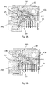
- Fig. 3A illustrates a first type of circuit wafer 40A with five high-frequency traces 305.
- Fig. 3B illustrates a second type of circuit wafer 40B with four high-frequency traces 310.
- the arrangement of the size and position of the top, middle, and bottom surface regions 220, 225 and 230 may be selected to prevent the first side 205 of the vertical member 215 from making direct contact with critical regions of either type of circuit wafer 40A and 40B.
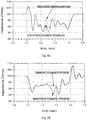
- Figs. 4A and 4B illustrate impedance waveforms simulated using a 16ps 20/80 rise time.
- the wave forms help illustrate the improvements in impedance that may be realized with the arrangements described above when compared to conventional connectors that utilize shrouds that do not have the features described above.
- the TDR pulse is injected into the backplane-side of both a conventional and improved connector; and in Fig. 4B , the TDR pulse is injected into the daughter card-side of both the conventional and improved connector.
- Both waveforms indicate about a 5 ohm improvement in the impedance, where the ideal impedance is 100 ohms.
Landscapes
- Details Of Connecting Devices For Male And Female Coupling (AREA)
- Coupling Device And Connection With Printed Circuit (AREA)
Abstract
Description
- The present invention relates generally to electrical connectors carrying high-frequency signals. More specifically, the present invention relates to an electrical connector with an improved shroud configuration that results in improved impedance characteristics.
- Some electrical systems incorporate a number of electrical modules that are interconnected with one another via a backplane circuit board. Connectors on the modules facilitate insertion of the modules into complementary connectors on the backplane.
- Each connector may be configured to couple one or more signals between the electrical module and the backplane. Signals transferred via the connector may be relatively high-frequency signals. Special care must be taken in the construction of the connector to minimize degradation of any signals communicated over the connector.
- The solution is provided by a shroud that forms part of an electrical connector for securing a plurality of circuit wafers within the electrical connector includes a top wall, a bottom wall, and a plurality of vertical members extending between the top and bottom walls that define a plurality of slots for receiving the plurality of circuit wafers. Each vertical member includes a first side that faces a second side of an adjacent vertical member. The first side defines top, middle, and bottom surface regions that are spaced apart from the second side of the adjacent vertical member by a first distance, and first and second recessed surface regions between the top, middle, and bottom surface regions that are spaced apart from the second side of the adjacent vertical member by a second distance that is greater than the first distance. The first and second recessed surface regions are positioned so as to prevent direct contact between the vertical members and one or more high-frequency traces disposed on the plurality of circuit wafers.
- The invention will now be described by way of example with reference to the accompanying drawings in which:
-
Fig. 1 illustrates a perspective view of an improved electrical connector formed in accordance with an exemplary embodiment that houses a plurality of the exemplary circuit wafers. -
Fig. 2A illustrates a front view of a shroud of the improved electrical connector when viewed in direction A ofFig. 1 ; -
Fig. 2B illustrates a cross-section of the shroud taken along section B-B' ofFig. 2A ; -
Fig. 2C illustrates a cross-section of the shroud taken along section C-C' ofFig. 2A ; -
Figs. 3A and 3B illustrate different circuit wafers positioned within the shroud of the improved electrical connector; and -
Figs. 4A and 4B illustrate impedance waveforms associated with the improved electrical connector and a conventional electrical connector. - In one aspect, a shroud that forms part of an electrical connector for securing a plurality of circuit wafers within the electrical connector includes a top wall, a bottom wall, and a plurality of vertical members extending between the top and bottom walls that define a plurality of slots for receiving the plurality of circuit wafers. Each vertical member includes a first side that faces a second side of an adjacent vertical member. The first side defines top, middle, and bottom surface regions that are spaced apart from the second side of the adjacent vertical member by a first distance, and first and second recessed surface regions between the top, middle, and bottom surface regions that are spaced apart from the second side of the adjacent vertical member by a second distance that is greater than the first distance. The first and second recessed surface regions are positioned so as to prevent direct contact between the vertical members and one or more high-frequency traces disposed on the plurality of circuit wafers.
- In a second aspect, an electrical connector includes a bottom housing, a plurality of circuit wafers disposed within the bottom housing, where each circuit wafer includes one or more high-frequency traces for communicating high-frequency signals. The electrical connector also includes a shroud that forms atop of the electrical connector that is configured to engage the bottom housing to secure the plurality of circuit wafers between the bottom housing and the shroud. The shroud includes a top wall, a bottom wall, and a plurality of vertical members that extend between the top and bottom walls that define a plurality of slots for maintaining spacing between the plurality of circuit wafers. Each vertical member includes a first side that faces a second side of an adjacent vertical member. The first side defines top, middle, and bottom surface regions that are spaced apart from the second side of the adjacent vertical member by a first distance, and first and second recessed surface regions between the top, middle, and bottom surface regions that are spaced apart from the second side of the adjacent vertical member by a second distance that is greater than the first distance. The first and second recessed surface regions are positioned so as to prevent direct contact between the vertical members and the one or more high-frequency traces disposed on the plurality of circuit wafers to thereby improve impedance characteristics of the electrical connector.
- In a third aspect, an electrical product includes an electrical connector. The electrical connector includes a bottom housing, a plurality of circuit wafers disposed within the bottom housing, where each circuit wafer includes one or more high-frequency traces for communicating high-frequency signals. The electrical connector also includes a shroud that forms atop of the electrical connector that is configured to engage the bottom housing to secure the plurality of circuit wafers between the bottom housing and the shroud. The shroud includes a top wall, a bottom wall, and a plurality of vertical members that extend between the top and bottom walls that define a plurality of slots for maintaining spacing between the plurality of circuit wafers. Each vertical member includes a first side that faces a second side of an adjacent vertical member. The first side defines top, middle, and bottom surface regions that are spaced apart from the second side of the adjacent vertical member by a first distance, and first and second recessed surface regions between the top, middle, and bottom surface regions that are spaced apart from the second side of the adjacent vertical member by a second distance that is greater than the first distance. The first and second recessed surface regions are positioned so as to prevent direct contact between the vertical members and the one or more high-frequency traces disposed on the plurality of circuit wafers to thereby improve impedance characteristics of the electrical connector.
-
Fig. 1 illustrates a perspective view of anelectrical connector 10 formed in accordance with an exemplary embodiment. Theelectrical connector 10 may be one of many disposed on a specialized circuit module to facilitate electrically coupling signals on the circuit module with other circuit modules via a backplane circuit board of a product such RF test equipment and the like. - The
connector 10 may correspond to a receptacle connector configured to be mounted on acircuit board 12 which in an exemplary embodiment is a daughter board. Theconnector 10 has amating face 14 and amounting face 16 that includes an interface for mounting theconnector 10 to thecircuit board 12. - In an exemplary embodiment, the
mounting face 16 is substantially perpendicular to themating face 14 such that thereceptacle connector 10 interconnects electrical components that are substantially at a right angle to each other. Themating face 14 of theconnector 10 defines a backplane connector interface. In one embodiment, theconnector 10 may be used to interconnect a daughter board to a backplane circuit board. In other embodiments, theconnector 10 may be configured to interconnect electrical components that are at other than a right angle to each other. - While the invention will be described in terms of a connector carrying differential signals, it is to be understood that the following description is for illustrative purposes only and is but one potential application of the inventive concepts herein. It is appreciated that the benefits and advantages of the invention may accrue equally to other types of signal connectors and wafer combinations.
- The
connector 10 includes adielectric housing 20 that has an upper housing portion orshroud 22 and a lower housing portion orbottom housing 24. Theshroud 22 includes top andbottom walls mating face 14 of theconnector 10. Thetop wall 26 andbottom wall 28 extend forwardly fromupper housing 22 in the direction of arrow A, which is also the mating direction of theconnector 10. - The
shroud 22 may includeend openings 30 at afirst end 32 and asecond end 34. Theshroud 22 andlower housing portion 24 are coupled together forming an open framework for holding a plurality ofcircuit wafers 40 that are received into thehousing 20 with a card edge connection. - The circuit wafers 40 include
signal contact pads 44,ground contact pads 46, and high-frequency traces for routing signals communicated via thecontact pads 44. - The
connector 10 is modular in construction; and in the embodiment shown inFig. 1 , includes twelvecircuit wafers 40. It is to be understood that in alternative embodiments, a greater or fewer number of thecircuit wafers 40 may be used. -
Fig. 2A illustrates a front view of theshroud 22 when viewed in direction A ofFig. 1 .Fig. 2B illustrates a cross-section view taken along section B-B' ofFig. 2A. Fig. 2C illustrates a cross-section view taken along section C-C' ofFig. 2A . - As noted above, the
shroud 22 corresponds to the top of theelectrical connector 10. Theshroud 22 is configured to cooperate with thelower housing portion 24 of theelectrical connector 10 to secure thecircuit wafers 40 between thelower housing portion 24 and theshroud 22. - Referring to
Figs. 2A-2C , theshroud 22 includes atop wall 26, abottom wall 28, and a plurality ofvertical members 215 that extend between the top andbottom walls vertical members 215 define a plurality ofslots 212 for receiving thecircuit wafers 40 and for maintaining spacing between thecircuit wafers 40. - Each
vertical member 215 includes afirst side 205 that faces asecond side 210 of an adjacent vertical member. Thefirst side 205 defines top, middle, andbottom surface regions second side 210 of the adjacent vertical member by a first distance, D1. Thefirst side 205 may also define first and second recessedsurface regions bottom surface regions second side 210 of thevertical member 215 may be generally flat or may have features similar to those found on thefirst side 205. - The first and second recessed
surface regions second side 210 of the adjacentvertical member 215 by a second distance, D2, that is greater than the first distance, D1. Distance D1 may generally correspond to the thickness of acircuit wafer 40 to facilitate a snug fit between theshroud 22 and thecircuit wafer 40. For example, for acircuit wafer 40 with a thickness of just under about .45mm, the first distance, D1, may be about .45mm to provide a snug fit. The second distance, D2, is selected to ensure that no portion of thevertical member 215 in the first and second recessedsurface regions circuit wafers 40. For example, the second distance, D2, may be about .60mm. This ensures that the first and second recessedsurface regions circuit wafer 40. - Referring to
Figs. 3A and 3B , the size and position of the top, middle, andbottom surface regions first side 205 of thevertical member 215 from making direct contact with critical regions of thecircuit wafer 40, such as regions where high-frequency traces 305 and 310 may be arranged, as illustrated. Stated differently, the arrangement of the top, middle, andbottom surface regions surface regions vertical members 215 are positioned over the critical regions of thecircuit wafer 40. Preventing contact between thevertical members 215 and thecircuit wafers 40 in the critical regions may help to improve the impedance characteristics of the electrical connector. - In one exemplary implementation, the
top surface region 220 may extend down from thetop wall 26 by a distance, L1, of about 3.12 mm. Thebottom surface region 230 may extend upward from thebottom wall 28 by a distance, L3, of about 2.22 mm. Themiddle surface region 225 may be vertically centered within thevertical member 215 and have a height, L2, of about 4.18 mm. This arrangement may provide for first and second recessedsurface regions - In some implementations, circuit wafers having different high-frequency trace arrangements may be utilized. For example,
Fig. 3A illustrates a first type ofcircuit wafer 40A with five high-frequency traces 305.Fig. 3B illustrates a second type ofcircuit wafer 40B with four high-frequency traces 310. In this case, the arrangement of the size and position of the top, middle, andbottom surface regions first side 205 of thevertical member 215 from making direct contact with critical regions of either type ofcircuit wafer -
Figs. 4A and 4B illustrate impedance waveforms simulated using a16ps 20/80 rise time. The wave forms help illustrate the improvements in impedance that may be realized with the arrangements described above when compared to conventional connectors that utilize shrouds that do not have the features described above. InFig. 4A , the TDR pulse is injected into the backplane-side of both a conventional and improved connector; and inFig. 4B , the TDR pulse is injected into the daughter card-side of both the conventional and improved connector. Both waveforms indicate about a 5 ohm improvement in the impedance, where the ideal impedance is 100 ohms. - While the shroud and electrical connector have been described with reference to certain embodiments and dimensions, it will be understood by those skilled in the art that various changes may be made and equivalents may be substituted without departing from the scope of the claims of the application. For example, one reason for providing the
middle surface region 225 is to provide additional support for thecircuit wafer 40. However, in circumstances where the extra support is not required, themiddle surface region 225 may be removed to provide a continuous recessed region between the top andbottom surface regions
Claims (9)
- A shroud (22) for forming part of an electrical connector (10) for securing a plurality of circuit wafers (40) within the electrical connector, the shroud comprising:a top wall (26);a bottom wall (28);a plurality of vertical members (215) extending between the top (26) and bottom (28) walls that define a plurality of slots (212) for receiving the plurality of circuit wafers (40), each vertical member (215) including a first side (205) that faces a second side (210) of an adjacent vertical member;wherein the first side (205) defines top (220), middle (225), and bottom (230) surface regions that are spaced apart from the second side (210) of the adjacent vertical member by a first distance (D1), and first (235) and second (240) recessed surface regions between the top (220), middle (225), and bottom (230) surface regions that are spaced apart from the second side (210) of the adjacent vertical member by a second distance (D2) that is greater than the first distance (D1), wherein the first (235) and second (240) recessed surface regions are positioned so as to prevent direct contact between the vertical members (215) and one or more high-frequency traces (305 and 310) disposed on the plurality of circuit wafers (40).
- The shroud according to claim 1, wherein the top surface region (220) extends from the top wall (26) to a top section of the first recessed surface region (235) and the bottom surface region (230) extends from the bottom wall (28) to a bottom section of the second recessed surface region (240).
- The shroud according to claim 1 or 2, wherein the middle surface region (225) is centered between the top wall (26) and the bottom wall (28).
- The shroud according to claim 1, 2 or 3, wherein a height of the first (235) and second (240) recessed surface regions is about 5.0 mm.
- The shroud according to any preceding claim, wherein the first distance (D1) is about 0.45 mm and the second distance (D2) is about 0.60 mm.
- The shroud according to any preceding claim, wherein a surface of the second side (210) is substantially flat.
- An electrical connector (10) comprising:a bottom housing (24);a plurality of circuit wafers (40) disposed within the bottom housing (24), each circuit wafer (40) including one or more high-frequency traces (305, 310) for communicating high-frequency signals; andthe shroud (22) according to any preceding claim, the shroud (22) forming a top of the electrical connector (10) that is configured to engage the bottom housing (24) to secure the plurality of circuit wafers (40) between the bottom housing (24) and the shroud (22).
- The electrical connector according to claim 7, wherein the first (235) and second (240) recessed surface regions positioned so as to prevent direct contact between the vertical members (215) and the one or more high-frequency traces (305, 310) disposed on the plurality of circuit wafers (40) thereby improve impedance characteristics of the electrical connector (10).
- The electrical connector according to claim 7 or 8, wherein the plurality of circuit wafers (40) includes a first group of circuit wafers (40A) and a second group of circuit wafers (40B), wherein an arrangement of the one or more high-frequency traces (305) on the first group of circuit wafers (40A) is different from an arrangement of the one or more high frequency traces (310) on the second group of circuit wafers (40B); and
wherein the first (235) and second (240) recessed surface regions of the vertical members (215) are arranged in a same relative position for each vertical member (215) and arranged so as to prevent direct contact between the vertical members (215) and the one or more high-frequency traces (305, 310) disposed on both the first and second group of circuit wafers (40A, 40B).
Applications Claiming Priority (1)
| Application Number | Priority Date | Filing Date | Title |
|---|---|---|---|
| US15/657,997 US9997868B1 (en) | 2017-07-24 | 2017-07-24 | Electrical connector with improved impedance characteristics |
Publications (2)
| Publication Number | Publication Date |
|---|---|
| EP3435495A1 true EP3435495A1 (en) | 2019-01-30 |
| EP3435495B1 EP3435495B1 (en) | 2021-02-17 |
Family
ID=62455225
Family Applications (1)
| Application Number | Title | Priority Date | Filing Date |
|---|---|---|---|
| EP18185252.6A Active EP3435495B1 (en) | 2017-07-24 | 2018-07-24 | Electrical connector with improved impedance characteristics |
Country Status (4)
| Country | Link |
|---|---|
| US (1) | US9997868B1 (en) |
| EP (1) | EP3435495B1 (en) |
| JP (1) | JP7078480B2 (en) |
| CN (1) | CN109301576B (en) |
Families Citing this family (3)
| Publication number | Priority date | Publication date | Assignee | Title |
|---|---|---|---|---|
| US10263352B2 (en) * | 2016-06-10 | 2019-04-16 | Te Connectivity Corporation | Electrical contact pad for electrically contacting a connector |
| US10879651B2 (en) * | 2016-06-18 | 2020-12-29 | Molex, Llc | Selectively shielded connector channel |
| US11297712B2 (en) * | 2020-03-26 | 2022-04-05 | TE Connectivity Services Gmbh | Modular printed circuit board wafer connector with reduced crosstalk |
Citations (2)
| Publication number | Priority date | Publication date | Assignee | Title |
|---|---|---|---|---|
| US6267604B1 (en) * | 2000-02-03 | 2001-07-31 | Tyco Electronics Corporation | Electrical connector including a housing that holds parallel circuit boards |
| US20050048842A1 (en) * | 2001-01-12 | 2005-03-03 | Litton Systems, Inc. | High-speed electrical connector |
Family Cites Families (43)
| Publication number | Priority date | Publication date | Assignee | Title |
|---|---|---|---|---|
| US3223960A (en) | 1962-12-07 | 1965-12-14 | Elco Corp | Contact with wave shaped tail sections |
| US5093640A (en) | 1989-09-29 | 1992-03-03 | Hewlett-Packard Company | Microstrip structure having contact pad compensation |
| US5692928A (en) | 1996-05-10 | 1997-12-02 | Molex Incorporated | Electrical connector having terminals with improved retention means |
| US5993259A (en) | 1997-02-07 | 1999-11-30 | Teradyne, Inc. | High speed, high density electrical connector |
| US6663442B1 (en) | 2000-01-27 | 2003-12-16 | Tyco Electronics Corporation | High speed interconnect using printed circuit board with plated bores |
| US6824391B2 (en) | 2000-02-03 | 2004-11-30 | Tyco Electronics Corporation | Electrical connector having customizable circuit board wafers |
| US6171115B1 (en) | 2000-02-03 | 2001-01-09 | Tyco Electronics Corporation | Electrical connector having circuit boards and keying for different types of circuit boards |
| US6655966B2 (en) | 2002-03-19 | 2003-12-02 | Tyco Electronics Corporation | Modular connector with grounding interconnect |
| US6843687B2 (en) * | 2003-02-27 | 2005-01-18 | Molex Incorporated | Pseudo-coaxial wafer assembly for connector |
| US7018246B2 (en) | 2003-03-14 | 2006-03-28 | Fci Americas Technology, Inc. | Maintenance of uniform impedance profiles between adjacent contacts in high speed grid array connectors |
| JP3964353B2 (en) * | 2003-05-22 | 2007-08-22 | タイコエレクトロニクスアンプ株式会社 | Connector assembly |
| EP1652273A4 (en) * | 2003-07-17 | 2008-01-02 | Winchester Electronics Corp | High-speed electrical connector |
| US6884117B2 (en) * | 2003-08-29 | 2005-04-26 | Hon Hai Precision Ind. Co., Ltd. | Electrical connector having circuit board modules positioned between metal stiffener and a housing |
| US6811440B1 (en) | 2003-08-29 | 2004-11-02 | Tyco Electronics Corporation | Power connector |
| US6875031B1 (en) * | 2003-12-05 | 2005-04-05 | Hon Hai Precision Ind. Co., Ltd. | Electrical connector with circuit board module |
| JP4133786B2 (en) | 2003-12-16 | 2008-08-13 | 日東電工株式会社 | Printed circuit board |
| US7044794B2 (en) | 2004-07-14 | 2006-05-16 | Tyco Electronics Corporation | Electrical connector with ESD protection |
| US7175445B2 (en) | 2004-08-31 | 2007-02-13 | Tyco Electronics Corporation | Electrical connector power wafers |
| US7371117B2 (en) * | 2004-09-30 | 2008-05-13 | Amphenol Corporation | High speed, high density electrical connector |
| JP2006210851A (en) | 2005-01-31 | 2006-08-10 | Toshiba Corp | Circuit board |
| WO2006105485A1 (en) * | 2005-03-31 | 2006-10-05 | Molex Incorporated | High-density, robust connector with dielectric insert |
| US8083553B2 (en) * | 2005-06-30 | 2011-12-27 | Amphenol Corporation | Connector with improved shielding in mating contact region |
| US7163421B1 (en) * | 2005-06-30 | 2007-01-16 | Amphenol Corporation | High speed high density electrical connector |
| US7326092B2 (en) | 2005-08-11 | 2008-02-05 | Tyco Electronics Corporation | Double ended guide pin assembly |
| KR100726458B1 (en) | 2006-01-16 | 2007-06-11 | 삼성전자주식회사 | Substrate Assembly |
| JPWO2008059571A1 (en) | 2006-11-15 | 2010-02-25 | パナソニック株式会社 | Circuit board connection structure and circuit board |
| DE102006062494A1 (en) | 2006-12-28 | 2008-07-03 | Robert Bosch Gmbh | Electric device with a carrier element with at least one special pad and a surface mounted device |
| US7722401B2 (en) * | 2007-04-04 | 2010-05-25 | Amphenol Corporation | Differential electrical connector with skew control |
| EP2240980A2 (en) | 2008-01-17 | 2010-10-20 | Amphenol Corporation | Electrical connector assembly |
| JP2009224564A (en) | 2008-03-17 | 2009-10-01 | Panasonic Corp | Wiring board, electronic device using the same and incorrect connection detector therefor |
| TWM353504U (en) | 2008-10-17 | 2009-03-21 | Wintek Corp | Card insertion terminal structure of flexible PCB |
| CN102598430B (en) | 2009-09-09 | 2015-08-12 | 安费诺有限公司 | For the compression contacts of high-speed electrical connectors |
| US9173292B1 (en) | 2011-03-11 | 2015-10-27 | Hittite Microwave Corporation | Edge launch transition for a printed circuit board |
| US9033750B2 (en) | 2012-08-15 | 2015-05-19 | Tyco Electronics Corporation | Electrical contact |
| CN105379023B (en) * | 2013-03-04 | 2018-09-18 | 3M创新有限公司 | Electric interconnection system and electric connector for the electric interconnection system |
| EP2775732B1 (en) | 2013-03-08 | 2016-02-03 | CCS Technology, Inc. | Protection device for a contact strip of a distribution device |
| CN105191003B (en) * | 2013-03-13 | 2017-12-08 | 安费诺有限公司 | Housing for high-speed electrical connectors |
| US9635759B2 (en) | 2013-08-16 | 2017-04-25 | Osram Sylvania Inc. | Conductor pad for flexible circuits and flexible circuit incorporating the same |
| JPWO2015029942A1 (en) | 2013-08-26 | 2017-03-02 | 京セラ株式会社 | High frequency circuit board, high frequency semiconductor package and high frequency semiconductor device using the same |
| US9288905B2 (en) | 2013-11-11 | 2016-03-15 | Seagate Technology Llc | Shaped internal leads for a printed circuit substrate |
| WO2015112717A1 (en) * | 2014-01-22 | 2015-07-30 | Amphenol Corporation | High speed, high density electrical connector with shielded signal paths |
| JP6299445B2 (en) | 2014-06-04 | 2018-03-28 | 日立金属株式会社 | Cable with connector and connector |
| US9859658B2 (en) * | 2015-05-14 | 2018-01-02 | Te Connectivity Corporation | Electrical connector having resonance controlled ground conductors |
-
2017
- 2017-07-24 US US15/657,997 patent/US9997868B1/en active Active
-
2018
- 2018-07-18 JP JP2018134613A patent/JP7078480B2/en active Active
- 2018-07-23 CN CN201810811556.7A patent/CN109301576B/en active Active
- 2018-07-24 EP EP18185252.6A patent/EP3435495B1/en active Active
Patent Citations (2)
| Publication number | Priority date | Publication date | Assignee | Title |
|---|---|---|---|---|
| US6267604B1 (en) * | 2000-02-03 | 2001-07-31 | Tyco Electronics Corporation | Electrical connector including a housing that holds parallel circuit boards |
| US20050048842A1 (en) * | 2001-01-12 | 2005-03-03 | Litton Systems, Inc. | High-speed electrical connector |
Also Published As
| Publication number | Publication date |
|---|---|
| JP2019024001A (en) | 2019-02-14 |
| JP7078480B2 (en) | 2022-05-31 |
| US9997868B1 (en) | 2018-06-12 |
| EP3435495B1 (en) | 2021-02-17 |
| CN109301576A (en) | 2019-02-01 |
| CN109301576B (en) | 2021-11-02 |
Similar Documents
| Publication | Publication Date | Title |
|---|---|---|
| CN109616791B (en) | Electrical connector having impedance control member at mating interface | |
| KR102888814B1 (en) | Connector assembly | |
| EP3391473B1 (en) | Backplane connector omitting ground shields and system using same | |
| CN105655785B (en) | Plug Transition Connectors for Electrical Connector Systems | |
| KR100768508B1 (en) | Header assembly for mounting to a circuit substrate | |
| US7651373B2 (en) | Board-to-board electrical connector | |
| CN103199386B (en) | Electric connector and assembly thereof | |
| US8298015B2 (en) | Electrical connector assembly with improved shield and shield coupling | |
| CN101779342B (en) | Connector with bifurcated contact arms | |
| CN105390887B (en) | High-Speed Signal Isolation Electrical Connector Assemblies | |
| US9490586B1 (en) | Electrical connector having a ground shield | |
| WO2016003663A1 (en) | Electrical connector with ground bus | |
| EP1939990A1 (en) | Connector apparatus | |
| WO2013119373A1 (en) | Midplane orthogonal connector system | |
| CN103066425B (en) | Electric coupler component | |
| KR20020073527A (en) | Connector with shielding | |
| WO2016168820A1 (en) | High density electrical connector with shield plate louvers | |
| EP3471216A1 (en) | Electrical connector | |
| EP3469861A1 (en) | Electrical contact pad for electrically contacting a connector | |
| EP3435495B1 (en) | Electrical connector with improved impedance characteristics | |
| EP2175526A1 (en) | Connector assembly having signal and coaxial contacts | |
| US9799995B1 (en) | Dual unibody USB connector | |
| US10263352B2 (en) | Electrical contact pad for electrically contacting a connector | |
| US8662932B2 (en) | Connector system using right angle, board-mounted connectors | |
| US9118147B1 (en) | Electrical connector |
Legal Events
| Date | Code | Title | Description |
|---|---|---|---|
| PUAI | Public reference made under article 153(3) epc to a published international application that has entered the european phase |
Free format text: ORIGINAL CODE: 0009012 |
|
| STAA | Information on the status of an ep patent application or granted ep patent |
Free format text: STATUS: THE APPLICATION HAS BEEN PUBLISHED |
|
| AK | Designated contracting states |
Kind code of ref document: A1 Designated state(s): AL AT BE BG CH CY CZ DE DK EE ES FI FR GB GR HR HU IE IS IT LI LT LU LV MC MK MT NL NO PL PT RO RS SE SI SK SM TR |
|
| AX | Request for extension of the european patent |
Extension state: BA ME |
|
| STAA | Information on the status of an ep patent application or granted ep patent |
Free format text: STATUS: REQUEST FOR EXAMINATION WAS MADE |
|
| 17P | Request for examination filed |
Effective date: 20190729 |
|
| RBV | Designated contracting states (corrected) |
Designated state(s): AL AT BE BG CH CY CZ DE DK EE ES FI FR GB GR HR HU IE IS IT LI LT LU LV MC MK MT NL NO PL PT RO RS SE SI SK SM TR |
|
| STAA | Information on the status of an ep patent application or granted ep patent |
Free format text: STATUS: EXAMINATION IS IN PROGRESS |
|
| 17Q | First examination report despatched |
Effective date: 20200706 |
|
| GRAP | Despatch of communication of intention to grant a patent |
Free format text: ORIGINAL CODE: EPIDOSNIGR1 |
|
| STAA | Information on the status of an ep patent application or granted ep patent |
Free format text: STATUS: GRANT OF PATENT IS INTENDED |
|
| INTG | Intention to grant announced |
Effective date: 20201116 |
|
| RIN1 | Information on inventor provided before grant (corrected) |
Inventor name: SMITH, GRAHAM HARRY, JR. Inventor name: TSANG, ALBERT Inventor name: WALTON, SCOTT ERIC |
|
| GRAS | Grant fee paid |
Free format text: ORIGINAL CODE: EPIDOSNIGR3 |
|
| GRAA | (expected) grant |
Free format text: ORIGINAL CODE: 0009210 |
|
| STAA | Information on the status of an ep patent application or granted ep patent |
Free format text: STATUS: THE PATENT HAS BEEN GRANTED |
|
| AK | Designated contracting states |
Kind code of ref document: B1 Designated state(s): AL AT BE BG CH CY CZ DE DK EE ES FI FR GB GR HR HU IE IS IT LI LT LU LV MC MK MT NL NO PL PT RO RS SE SI SK SM TR |
|
| REG | Reference to a national code |
Ref country code: GB Ref legal event code: FG4D |
|
| REG | Reference to a national code |
Ref country code: CH Ref legal event code: EP |
|
| REG | Reference to a national code |
Ref country code: DE Ref legal event code: R096 Ref document number: 602018012544 Country of ref document: DE |
|
| REG | Reference to a national code |
Ref country code: AT Ref legal event code: REF Ref document number: 1362713 Country of ref document: AT Kind code of ref document: T Effective date: 20210315 |
|
| REG | Reference to a national code |
Ref country code: IE Ref legal event code: FG4D |
|
| REG | Reference to a national code |
Ref country code: LT Ref legal event code: MG9D |
|
| REG | Reference to a national code |
Ref country code: NL Ref legal event code: MP Effective date: 20210217 |
|
| PG25 | Lapsed in a contracting state [announced via postgrant information from national office to epo] |
Ref country code: BG Free format text: LAPSE BECAUSE OF FAILURE TO SUBMIT A TRANSLATION OF THE DESCRIPTION OR TO PAY THE FEE WITHIN THE PRESCRIBED TIME-LIMIT Effective date: 20210517 Ref country code: GR Free format text: LAPSE BECAUSE OF FAILURE TO SUBMIT A TRANSLATION OF THE DESCRIPTION OR TO PAY THE FEE WITHIN THE PRESCRIBED TIME-LIMIT Effective date: 20210518 Ref country code: HR Free format text: LAPSE BECAUSE OF FAILURE TO SUBMIT A TRANSLATION OF THE DESCRIPTION OR TO PAY THE FEE WITHIN THE PRESCRIBED TIME-LIMIT Effective date: 20210217 Ref country code: FI Free format text: LAPSE BECAUSE OF FAILURE TO SUBMIT A TRANSLATION OF THE DESCRIPTION OR TO PAY THE FEE WITHIN THE PRESCRIBED TIME-LIMIT Effective date: 20210217 Ref country code: LT Free format text: LAPSE BECAUSE OF FAILURE TO SUBMIT A TRANSLATION OF THE DESCRIPTION OR TO PAY THE FEE WITHIN THE PRESCRIBED TIME-LIMIT Effective date: 20210217 Ref country code: PT Free format text: LAPSE BECAUSE OF FAILURE TO SUBMIT A TRANSLATION OF THE DESCRIPTION OR TO PAY THE FEE WITHIN THE PRESCRIBED TIME-LIMIT Effective date: 20210617 Ref country code: NO Free format text: LAPSE BECAUSE OF FAILURE TO SUBMIT A TRANSLATION OF THE DESCRIPTION OR TO PAY THE FEE WITHIN THE PRESCRIBED TIME-LIMIT Effective date: 20210517 |
|
| REG | Reference to a national code |
Ref country code: AT Ref legal event code: MK05 Ref document number: 1362713 Country of ref document: AT Kind code of ref document: T Effective date: 20210217 |
|
| PG25 | Lapsed in a contracting state [announced via postgrant information from national office to epo] |
Ref country code: LV Free format text: LAPSE BECAUSE OF FAILURE TO SUBMIT A TRANSLATION OF THE DESCRIPTION OR TO PAY THE FEE WITHIN THE PRESCRIBED TIME-LIMIT Effective date: 20210217 Ref country code: PL Free format text: LAPSE BECAUSE OF FAILURE TO SUBMIT A TRANSLATION OF THE DESCRIPTION OR TO PAY THE FEE WITHIN THE PRESCRIBED TIME-LIMIT Effective date: 20210217 Ref country code: NL Free format text: LAPSE BECAUSE OF FAILURE TO SUBMIT A TRANSLATION OF THE DESCRIPTION OR TO PAY THE FEE WITHIN THE PRESCRIBED TIME-LIMIT Effective date: 20210217 Ref country code: RS Free format text: LAPSE BECAUSE OF FAILURE TO SUBMIT A TRANSLATION OF THE DESCRIPTION OR TO PAY THE FEE WITHIN THE PRESCRIBED TIME-LIMIT Effective date: 20210217 Ref country code: SE Free format text: LAPSE BECAUSE OF FAILURE TO SUBMIT A TRANSLATION OF THE DESCRIPTION OR TO PAY THE FEE WITHIN THE PRESCRIBED TIME-LIMIT Effective date: 20210217 |
|
| PG25 | Lapsed in a contracting state [announced via postgrant information from national office to epo] |
Ref country code: IS Free format text: LAPSE BECAUSE OF FAILURE TO SUBMIT A TRANSLATION OF THE DESCRIPTION OR TO PAY THE FEE WITHIN THE PRESCRIBED TIME-LIMIT Effective date: 20210617 |
|
| PG25 | Lapsed in a contracting state [announced via postgrant information from national office to epo] |
Ref country code: EE Free format text: LAPSE BECAUSE OF FAILURE TO SUBMIT A TRANSLATION OF THE DESCRIPTION OR TO PAY THE FEE WITHIN THE PRESCRIBED TIME-LIMIT Effective date: 20210217 Ref country code: CZ Free format text: LAPSE BECAUSE OF FAILURE TO SUBMIT A TRANSLATION OF THE DESCRIPTION OR TO PAY THE FEE WITHIN THE PRESCRIBED TIME-LIMIT Effective date: 20210217 Ref country code: SM Free format text: LAPSE BECAUSE OF FAILURE TO SUBMIT A TRANSLATION OF THE DESCRIPTION OR TO PAY THE FEE WITHIN THE PRESCRIBED TIME-LIMIT Effective date: 20210217 Ref country code: AT Free format text: LAPSE BECAUSE OF FAILURE TO SUBMIT A TRANSLATION OF THE DESCRIPTION OR TO PAY THE FEE WITHIN THE PRESCRIBED TIME-LIMIT Effective date: 20210217 |
|
| REG | Reference to a national code |
Ref country code: DE Ref legal event code: R097 Ref document number: 602018012544 Country of ref document: DE |
|
| PG25 | Lapsed in a contracting state [announced via postgrant information from national office to epo] |
Ref country code: DK Free format text: LAPSE BECAUSE OF FAILURE TO SUBMIT A TRANSLATION OF THE DESCRIPTION OR TO PAY THE FEE WITHIN THE PRESCRIBED TIME-LIMIT Effective date: 20210217 Ref country code: SK Free format text: LAPSE BECAUSE OF FAILURE TO SUBMIT A TRANSLATION OF THE DESCRIPTION OR TO PAY THE FEE WITHIN THE PRESCRIBED TIME-LIMIT Effective date: 20210217 Ref country code: RO Free format text: LAPSE BECAUSE OF FAILURE TO SUBMIT A TRANSLATION OF THE DESCRIPTION OR TO PAY THE FEE WITHIN THE PRESCRIBED TIME-LIMIT Effective date: 20210217 |
|
| PLBE | No opposition filed within time limit |
Free format text: ORIGINAL CODE: 0009261 |
|
| STAA | Information on the status of an ep patent application or granted ep patent |
Free format text: STATUS: NO OPPOSITION FILED WITHIN TIME LIMIT |
|
| 26N | No opposition filed |
Effective date: 20211118 |
|
| PG25 | Lapsed in a contracting state [announced via postgrant information from national office to epo] |
Ref country code: ES Free format text: LAPSE BECAUSE OF FAILURE TO SUBMIT A TRANSLATION OF THE DESCRIPTION OR TO PAY THE FEE WITHIN THE PRESCRIBED TIME-LIMIT Effective date: 20210217 Ref country code: AL Free format text: LAPSE BECAUSE OF FAILURE TO SUBMIT A TRANSLATION OF THE DESCRIPTION OR TO PAY THE FEE WITHIN THE PRESCRIBED TIME-LIMIT Effective date: 20210217 |
|
| PG25 | Lapsed in a contracting state [announced via postgrant information from national office to epo] |
Ref country code: SI Free format text: LAPSE BECAUSE OF FAILURE TO SUBMIT A TRANSLATION OF THE DESCRIPTION OR TO PAY THE FEE WITHIN THE PRESCRIBED TIME-LIMIT Effective date: 20210217 |
|
| REG | Reference to a national code |
Ref country code: CH Ref legal event code: PL |
|
| PG25 | Lapsed in a contracting state [announced via postgrant information from national office to epo] |
Ref country code: MC Free format text: LAPSE BECAUSE OF FAILURE TO SUBMIT A TRANSLATION OF THE DESCRIPTION OR TO PAY THE FEE WITHIN THE PRESCRIBED TIME-LIMIT Effective date: 20210217 |
|
| REG | Reference to a national code |
Ref country code: BE Ref legal event code: MM Effective date: 20210731 |
|
| PG25 | Lapsed in a contracting state [announced via postgrant information from national office to epo] |
Ref country code: LI Free format text: LAPSE BECAUSE OF NON-PAYMENT OF DUE FEES Effective date: 20210731 Ref country code: IT Free format text: LAPSE BECAUSE OF FAILURE TO SUBMIT A TRANSLATION OF THE DESCRIPTION OR TO PAY THE FEE WITHIN THE PRESCRIBED TIME-LIMIT Effective date: 20210217 Ref country code: CH Free format text: LAPSE BECAUSE OF NON-PAYMENT OF DUE FEES Effective date: 20210731 |
|
| PG25 | Lapsed in a contracting state [announced via postgrant information from national office to epo] |
Ref country code: IS Free format text: LAPSE BECAUSE OF FAILURE TO SUBMIT A TRANSLATION OF THE DESCRIPTION OR TO PAY THE FEE WITHIN THE PRESCRIBED TIME-LIMIT Effective date: 20210617 Ref country code: LU Free format text: LAPSE BECAUSE OF NON-PAYMENT OF DUE FEES Effective date: 20210724 |
|
| PG25 | Lapsed in a contracting state [announced via postgrant information from national office to epo] |
Ref country code: IE Free format text: LAPSE BECAUSE OF NON-PAYMENT OF DUE FEES Effective date: 20210724 Ref country code: BE Free format text: LAPSE BECAUSE OF NON-PAYMENT OF DUE FEES Effective date: 20210731 |
|
| PG25 | Lapsed in a contracting state [announced via postgrant information from national office to epo] |
Ref country code: CY Free format text: LAPSE BECAUSE OF FAILURE TO SUBMIT A TRANSLATION OF THE DESCRIPTION OR TO PAY THE FEE WITHIN THE PRESCRIBED TIME-LIMIT Effective date: 20210217 |
|
| PG25 | Lapsed in a contracting state [announced via postgrant information from national office to epo] |
Ref country code: HU Free format text: LAPSE BECAUSE OF FAILURE TO SUBMIT A TRANSLATION OF THE DESCRIPTION OR TO PAY THE FEE WITHIN THE PRESCRIBED TIME-LIMIT; INVALID AB INITIO Effective date: 20180724 |
|
| PG25 | Lapsed in a contracting state [announced via postgrant information from national office to epo] |
Ref country code: MK Free format text: LAPSE BECAUSE OF FAILURE TO SUBMIT A TRANSLATION OF THE DESCRIPTION OR TO PAY THE FEE WITHIN THE PRESCRIBED TIME-LIMIT Effective date: 20210217 |
|
| PG25 | Lapsed in a contracting state [announced via postgrant information from national office to epo] |
Ref country code: TR Free format text: LAPSE BECAUSE OF FAILURE TO SUBMIT A TRANSLATION OF THE DESCRIPTION OR TO PAY THE FEE WITHIN THE PRESCRIBED TIME-LIMIT Effective date: 20210217 |
|
| PG25 | Lapsed in a contracting state [announced via postgrant information from national office to epo] |
Ref country code: MT Free format text: LAPSE BECAUSE OF FAILURE TO SUBMIT A TRANSLATION OF THE DESCRIPTION OR TO PAY THE FEE WITHIN THE PRESCRIBED TIME-LIMIT Effective date: 20210217 |
|
| PGFP | Annual fee paid to national office [announced via postgrant information from national office to epo] |
Ref country code: GB Payment date: 20250605 Year of fee payment: 8 |
|
| PGFP | Annual fee paid to national office [announced via postgrant information from national office to epo] |
Ref country code: FR Payment date: 20250610 Year of fee payment: 8 |
|
| REG | Reference to a national code |
Ref country code: GB Ref legal event code: 732E Free format text: REGISTERED BETWEEN 20250731 AND 20250806 |
|
| PGFP | Annual fee paid to national office [announced via postgrant information from national office to epo] |
Ref country code: DE Payment date: 20250604 Year of fee payment: 8 |