EP3433914B1 - Maximizing power in a photovoltaic distributed power system - Google Patents
Maximizing power in a photovoltaic distributed power system Download PDFInfo
- Publication number
- EP3433914B1 EP3433914B1 EP17724234.4A EP17724234A EP3433914B1 EP 3433914 B1 EP3433914 B1 EP 3433914B1 EP 17724234 A EP17724234 A EP 17724234A EP 3433914 B1 EP3433914 B1 EP 3433914B1
- Authority
- EP
- European Patent Office
- Prior art keywords
- power
- string
- voltage
- output
- photovoltaic
- Prior art date
- Legal status (The legal status is an assumption and is not a legal conclusion. Google has not performed a legal analysis and makes no representation as to the accuracy of the status listed.)
- Active
Links
Images











Classifications
-
- G—PHYSICS
- G05—CONTROLLING; REGULATING
- G05F—SYSTEMS FOR REGULATING ELECTRIC OR MAGNETIC VARIABLES
- G05F1/00—Automatic systems in which deviations of an electric quantity from one or more predetermined values are detected at the output of the system and fed back to a device within the system to restore the detected quantity to its predetermined value or values, i.e. retroactive systems
- G05F1/66—Regulating electric power
- G05F1/67—Regulating electric power to the maximum power available from a generator, e.g. from solar cell
-
- H—ELECTRICITY
- H02—GENERATION; CONVERSION OR DISTRIBUTION OF ELECTRIC POWER
- H02J—ELECTRIC POWER NETWORKS; CIRCUIT ARRANGEMENTS OR SYSTEMS FOR SUPPLYING OR DISTRIBUTING ELECTRIC POWER; SYSTEMS FOR STORING ELECTRIC ENERGY
- H02J3/00—Circuit arrangements for AC mains or AC distribution networks
- H02J3/38—Arrangements for feeding a single network from two or more generators or sources in parallel; Arrangements for feeding already energised networks from additional generators or sources in parallel
- H02J3/381—Dispersed generators
-
- H—ELECTRICITY
- H02—GENERATION; CONVERSION OR DISTRIBUTION OF ELECTRIC POWER
- H02J—ELECTRIC POWER NETWORKS; CIRCUIT ARRANGEMENTS OR SYSTEMS FOR SUPPLYING OR DISTRIBUTING ELECTRIC POWER; SYSTEMS FOR STORING ELECTRIC ENERGY
- H02J3/00—Circuit arrangements for AC mains or AC distribution networks
- H02J3/38—Arrangements for feeding a single network from two or more generators or sources in parallel; Arrangements for feeding already energised networks from additional generators or sources in parallel
- H02J3/46—Controlling the sharing of generated power between the generators, sources or networks
-
- H—ELECTRICITY
- H10—SEMICONDUCTOR DEVICES; ELECTRIC SOLID-STATE DEVICES NOT OTHERWISE PROVIDED FOR
- H10F—INORGANIC SEMICONDUCTOR DEVICES SENSITIVE TO INFRARED RADIATION, LIGHT, ELECTROMAGNETIC RADIATION OF SHORTER WAVELENGTH OR CORPUSCULAR RADIATION
- H10F19/00—Integrated devices, or assemblies of multiple devices, comprising at least one photovoltaic cell covered by group H10F10/00, e.g. photovoltaic modules
-
- H—ELECTRICITY
- H02—GENERATION; CONVERSION OR DISTRIBUTION OF ELECTRIC POWER
- H02J—ELECTRIC POWER NETWORKS; CIRCUIT ARRANGEMENTS OR SYSTEMS FOR SUPPLYING OR DISTRIBUTING ELECTRIC POWER; SYSTEMS FOR STORING ELECTRIC ENERGY
- H02J2101/00—Supply or distribution of decentralised, dispersed or local electric power generation
- H02J2101/20—Dispersed power generation using renewable energy sources
- H02J2101/22—Solar energy
- H02J2101/24—Photovoltaics
- H02J2101/25—Photovoltaics involving maximum power point tracking control for photovoltaic sources
-
- Y—GENERAL TAGGING OF NEW TECHNOLOGICAL DEVELOPMENTS; GENERAL TAGGING OF CROSS-SECTIONAL TECHNOLOGIES SPANNING OVER SEVERAL SECTIONS OF THE IPC; TECHNICAL SUBJECTS COVERED BY FORMER USPC CROSS-REFERENCE ART COLLECTIONS [XRACs] AND DIGESTS
- Y02—TECHNOLOGIES OR APPLICATIONS FOR MITIGATION OR ADAPTATION AGAINST CLIMATE CHANGE
- Y02E—REDUCTION OF GREENHOUSE GAS [GHG] EMISSIONS, RELATED TO ENERGY GENERATION, TRANSMISSION OR DISTRIBUTION
- Y02E10/00—Energy generation through renewable energy sources
- Y02E10/50—Photovoltaic [PV] energy
- Y02E10/56—Power conversion systems, e.g. maximum power point trackers
Definitions
- Photovoltaic (PV) power devices can be used to improve the performance and to reduce the cost of power generation systems including photovoltaic panels.
- Photovoltaic power devices can be variously configured. The cost of some power devices may be proportional to the amount of electrical power they process. Thus, significant savings can be realized by designing systems to optimize output power while processing a small portion of the system power.
- the exemplary features presented relate to a photovoltaic power harvesting system including multiple photovoltaic strings and, more particularly to system and method for maximizing power in each photovoltaic string.
- FIG. 1 shows a photovoltaic power harvesting system 10 according to conventional art.
- a photovoltaic string 109 includes a series connection of photovoltaic panels 101. Photovoltaic strings 109 may be connected in parallel to give a parallel direct current (DC) power output.
- the parallel DC power output connects to the input of a direct current (DC) to alternating current (AC) inverter 103.
- the AC power output of inverter 103 connects across an AC load 105.
- AC load 105 may be an AC load such as an AC motor or may be an electrical power grid.
- three strings 109 may be used with an inverter 103. If two strings 109 are equally irradiated such that each string operates with a string voltage of 600 volts (V) and string current of 10 amperes (A); each of the two strings generates (10 A ⁇ 600 V) 6 kilowatts (kW). It is also assumed that the two equally irradiated strings 109 may be operating at maximum power.
- one string 109 is partially shaded or if one or more panels 101 is under performing, there may still be a string voltage of 600V as set by the other two equally irradiated strings 109, however, the string current in the one under performing string 109 may only be only 6 amperes.
- the under performing string 109 is not operating at maximum power point. For instance, it may be that the under performing string 109 has a maximum power point of 550 volts for a current of 10 amperes. In this situation, the power lost by the under performing string 109 is 1.9kW (550V ⁇ 10A - 600V ⁇ 6A). The under performing string 109, therefore, produces 3.6kW (600V ⁇ 6A). Overall power harvested from system 10 is, therefore 15.6kW (3.6kW + 2 ⁇ 6kW).
- FIG. 2 shows another power harvesting system 20 according to conventional art, according to international patent application publication WO2010002960 .
- System 20 is directed to reduce power losses compared to the losses of system 10.
- Each photovoltaic string 109 includes a series connection of photovoltaic panels 101.
- Each photovoltaic string 109 is connected in parallel to an input of a DC-to-DC converter 205.
- the output of converter 205 connects to a DC bus 211.
- the DC voltage generated by photovoltaic string 109 is converted by converter 205 to the voltage of DC bus 211.
- Each photovoltaic string 109 together with the respective DC-DC converter 205 forms a photovoltaic string module 207.
- a number of modules 207 with outputs from respective DC-to-DC converters 205 may be connected in parallel to DC bus 211.
- the parallel combined outputs of modules 207 may be also connected to an input of a direct current (DC) to alternating current (AC) inverter 103 via DC bus 211.
- Inverter 103 converts the combined DC power outputs of modules 207 to an alternating current power at an output of inverter 103.
- the output of inverter 103 connects to AC load 105.
- three modules 207 may be used with inverter 103.
- Two strings 109 may be equally irradiated such that each string of the two strings operates with a string voltage of 600 volts and string current of 10 amperes.
- Each of the two strings generates (10 amperes . 600 volts) or 6 kilowatts. If the one remaining string 109 is under performing, there may be maximum power point for the under performing string 109 of 550 volts and current of 10 amperes.
- Each DC-to-DC converter 205 may be configured to maximize power on each respective output to give 600 volts on DC bus 211.
- the two equally irradiated modules 207 each produce 6 kW (10 amperes ⁇ 600 volts) and the under performing unit 207 produces 5.5 kW (10 amperes ⁇ 550 volts). Giving an overall power harvested from system 20 of 17.5 kW. It can be seen that system 20 offers an improvement of 1.9kW over system 10 in terms of minimized losses and increased power harvested. The improvement has been achieved through multiple DC-DC converters 205 which operate at wattage levels of around 6 kW.
- the high power DC-DC converters 205 in a power harvesting system may add to the cost of installation and maintenance of the power harvesting system and may present an overall decreased level of reliability for the power harvesting system because DC-DC converters 205 operate at high wattage levels.
- US2013/193765 discloses system comprising: a plurality of parallel-connected compensated photovoltaic strings, each compensated photovoltaic string including: a photovoltaic string having a series-connection of photovoltaic cells; and a voltage-compensation circuit having a voltage output connected in series with said photovoltaic string, wherein said voltage-compensation circuit includes an input connected to a source of power separate from power provided by the photovoltaic string, wherein the voltage-compensation circuit is configured to provide at the voltage output an adjustable compensation voltage in series with a voltage generated by said photovoltaic string such that a total voltage of the compensated photovoltaic string maintains a predetermined value.
- HUIMIN ZHOU ET AL "PV Balancers: Concept, Architectures, and Realization", IEEE TRANSACTIONS ON POWER ELECTRONICS, USA, vol. 30, no. 7, doi:10.1109/TPEL.2014.2343615, ISSN 0885-8993, pages 3479 - 3487 , discloses PV balancers that are DC-DC converters, which are integrated into each module, and combined into a common DC bus configuration.
- HUIMIN ZHOU ET AL "PV balancers: Concept, architectures, and realization", ENERGY CONVERSION CONGRESS AND EXPOSITION (ECCE), 2012 IEEE, IEEE, doi:10.1109/ECCE.2012.6342469, ISBN 978-1-4673-0802-1, pages 3749 - 3755 , discloses PV balancers that are DC-DC converters, which are integrated into each module, and combined into a common DC bus configuration.
- US2010/126550 discloses an apparatus that controls the power produced by a string of solar cells, enabling the string to operate at its maximum power point when connected to a bus that operates at an externally controlled voltage.
- the apparatus can also be used to increase or decrease the output power of a string to any desired operating point.
- US2015/364918 discloses a system for optimizing load current in a string of solar panels.
- a string of solar panels includes a microprocessor coupled to the string of solar panels.
- the system includes a first DC-to-DC converter comprising input terminals coupled to a load and output terminals coupled to each solar panel in the string of solar panels.
- the first DC-to-DC converter is operable to supply a compensatory power for compensating a drop in the peak current arising due to shading of one or more solar panels.
- the system includes a second DC-to-DC converter coupled to the first DC-to-DC converter.
- the second DC-to-DC converter is operable as one of a voltage adder and a voltage subtractor to generate a compensatory voltage for compensating a drop in the load current arising due to panel mismatch among the string of solar panels.
- power grid and “mains grid” are used herein interchangeably and refer to a source of alternating current (AC) power provided by a power supply company.
- AC alternating current
- converter as used herein applies to DC-to-DC converters, AC-to-DC converters, DC-to-AC inverters, buck converters, boost converters, buck-boost converters, full-bridge converters and half-bridge converters or any other circuit for electrical power conversion/inversion known in the art.
- DC load as used herein applies to the DC inputs of converters, batteries, DC motors or DC generators.
- AC load as used herein applies to the AC inputs of converters, transformers, AC motors or AC generators.
- features of the present invention are directed towards maximizing output power from under-performing or partially shaded photovoltaic strings in a power harvesting system of parallel connected photovoltaic strings.
- the features may provide maximal overall power output of the system and reduced installation and maintenance cost of the system.
- the features may also provide increased reliability of the system, owing to lower power operating levels of switching converters added to each of the photovoltaic string compared with DC-DC converters 205 used in conventional system 20.
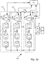
- FIG. 3a shows a power harvesting system 30a according to a feature of the present invention.
- a number of photovoltaic panels 101 are connected in series to form a photovoltaic string 109.
- String 109 is connected in series with a voltage-compensation circuit 307 to provide a compensated string 315.
- a source voltage (Vs) may be input to voltage-compensation circuit 307.
- a number of compensated strings 315 are connected together in parallel to give direct current (DC) power output 211.
- a power sensor 370 operatively connected to central controller 313 measures the power on DC output 211.
- DC power output 211 is connected to an input of a DC to alternating current (AC) inverter 103.
- AC alternating current
- Inverter 103 converts the combined DC power output 211 of strings 315 to an alternating current power at an output of inverter 103.
- the output of inverter 103 connects to AC load 105.
- a central controller 313 may be operatively attached to each voltage-compensation circuit 307 by bi-directional control and communication lines as shown, by wireless communication or by power line communications in DC bus 211.
- Central controller 313 may include a microprocessor with on-board memory and an interface which may include analogue to digital converters (ADCs) and digital to analogue converters (DACs).
- ADCs analogue to digital converters
- DACs digital to analogue converters
- Fig. 3b shows a power harvesting system 30b according to another feature of the present invention.
- String 109 is connected in series with voltage-compensation circuit 307 to provide a compensated string 315.
- a source voltage (Vs) is input to voltage-compensation circuit 307.
- a number of compensated strings 315 are connected together in parallel to give direct current (DC) power output 211.
- DC power output 211 is connected to an input of a DC to alternating current (AC) inverter 103.
- Inverter 103 converts the combined DC power output 211 of strings 315 to an alternating current power at an output of inverter 103.
- the output of inverter 103 connects to AC load 105.
- System 30a is the same as system 30b except that system 30b does not have central controller 313. Instead, monitoring and control in system 30b is performed by each circuit 307, which may include a microprocessor with on-board memory and an interface which may include analogue to digital converters (ADCs) and digital to analogue converters (DACs). Each circuit 307 is operatively attached to sensors 320, 322 and 324. Sensors 320 and 322 may be adapted to sense the voltage across photovoltaic string 109 as well as current in string 109. Alternatively, sensors 320 and 324 may be adapted to sense the voltage across a compensated string 315 and current in string 315. Alternatively, sensors 324 and 322 may be adapted to sense the voltage (Vc) across a circuit 307 as well as current through the circuit 307.
- ADCs analogue to digital converters
- DACs digital to analogue converters
- Voltage-compensation circuit 307 may be implemented using a direct current (DC) to DC converter 307a.
- DC-to-DC converter 307a may be a buck circuit, a boost circuit, a buck + boost circuit or switched-mode power supply (SMPS).
- the output of DC-to-DC converter 307 is connected in series within string 315 to add compensation voltage (Vc) to string 315.
- the DC source voltage input (Vs) to DC-to DC converter 307 may be provided from the combined DC output of strings 315, or strings 109.
- DC source voltage input may be provided by a micro-inverter converting AC from the mains grid or another independent source of DC power such as a battery or DC generator.
- Circuit 307 as shown in Fig. 3c is a conventional buck-boost DC- to-DC converter circuit which has an input voltage Vs with an input capacitor C 1 connected in parallel across Vs.
- Two switches may be implemented as field effect transistors (FET) with integral diodes: a high side buck switch Q 1 and a low side buck switch Q 2 connected in series by connecting the source of Q 1 to the drain of Q 2 .
- the drain of Q 1 and the source of Q 2 may be connected parallel across the input capacitor C 1 .
- a node A is formed between switches Q 1 and Q 2 to which one end of an inductor L is connected.
- the other end of inductor L is connected to the boost circuit of buck-boost DC-to-DC converter 307 at a node B.
- Node B connects two switches implemented as field effect transistors (FET): a high side boost switch Q 4 and a low side boost switch Q 3 together in series where the source of Q 4 connects to the drain of Q 3 to form node B.
- the drain of Q 4 and the source of Q 3 connect across an output capacitor C 2 to produce the output voltage V C of buck-boost DC-to-DC converter 307.
- Voltage compensation circuit 307 may be implemented using an alternating current (AC) to DC inverter.
- the AC to DC inverter 307b may be a type of switched mode power supply (SMPS).
- SMPS switched mode power supply
- voltage-compensation circuit 307 is an AC to DC converter 307b
- the DC output of the AC to DC converter is connected in series within a string 315.
- the AC input (Vs) to the AC to DC converter may be provided from the mains grid, from the AC output of inverter 103 or by another independent source of AC power.
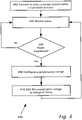
- Fig. 4 shows a method 400 which may be applied to power harvesting system 30b shown in Fig. 3b , according to a feature of the present invention.
- an output voltage (Vc) of circuit 307 is wired in series with a series-connection of panels 101 to form compensated string 315.
- the input voltage (Vs) to circuit 307 may be from direct current (DC) output 211, the alternating current (AC) output of inverter 103 or a separate independent AC or DC electric supply.
- Several compensated strings 315 outputs may then be connected in parallel and further connected to the input of an inverter 103 as shown in Fig. 3b .
- a circuit parameter of each parallel connected string 315 is monitored in the case of system 30b.
- the circuit parameter may be the current flowing in a string 315, the voltage across a string 315, the voltage of a photovoltaic string 109 and/or the voltage (Vc) across a circuit 307.
- the current and voltages in a string 315 may be used to determine the power (P) in a string 315 or a photovoltaic string 109 by virtue of power being equal to voltage (V) multiplied by current (I).
- a control algorithm stored in a circuit 307 adjusts compensation voltage V C to maximize output power of string 315.
- a compensation voltage V c for strings 315 is configured based on the result of the control algorithm performed in steps 404 and 406.
- the compensation voltage V c for strings 315 in step 408 may be a positive or a negative voltage polarity with respect to the voltage polarity of a string 109.
- the compensation voltage V c is added to string 315. In the case of the positive voltage for V c , the voltage of a string 315 may be increased in step 408. In the case of the negative voltage for V c , the voltage of string 315 may be decreased in step 408.
- Method 400 may also be applied to system 30a ( Fig. 3a ) which uses central controller 313.
- central controller monitors or calculates a net total power from system 30a.
- the net total power from system 30a is equal to the power produced by strings 109 subtracted from the power added by compensation circuits 307.
- Vs voltage (Vs) and hence power to the input of circuit 307 is derived from DC bus 211 or the output of inverter 103 to give compensated voltage (Vc).
- Vc compensated voltage
- the net total power from system 30a may be derived directly by monitoring (step 404) power on DC bus 211.
- Vs voltage (Vs) and hence power to the input of circuit 307 is derived from an independent DC source or AC source such as a mains supply to give compensated voltage (Vc).
- Vc compensated voltage
- the net total power from system 30a may be derived by subtracting power monitored on DC Bus 211 (step 404) from the power added by compensation circuits 307.
- compensation voltages V c of all strings 315 may be adjusted to maximize the net total power from system 30a.
- a compensation voltage V c for a string 315 is configured based on the result of the control algorithm performed in steps 404 and 406.
- the compensation voltage V c is added to a string 315.
- the control algorithm maintains strings 315 at their maximum power point (MPP) by adding compensation voltage to each string 315 to maintain maximum power from each string 315.
- MPP maximum power point
- no voltage compensation V c may be required and voltage compensation V c added to string 315 is at or near zero volts.
- circuit 307 which may be an AC to DC converter powered from the grid. Therefore, circuit 307 receives and converts voltage (Vs) and hence power from the electrical grid. If two strings 109 are equally irradiated such that each string operates with a string 109 voltage of 600 volts and string current of 10 amperes, each of the two strings generates (10 amperes ⁇ 600 volts) 6 kilowatts.
- one under-performing string 109 is partially shaded or if a panel 101 is removed or bypassed, there may be a string voltage of 550 Volts and current of 10 amperes, which means (10 amperes ⁇ 550 volts) 5.5 kilowatts may be generated by the under-performing string 109.
- the maximum power 5.5 kilowatts may be generated by the under-performing string 109 only if the under-performing string 109 can be operated at maximum power point (MPP).
- Voltage-compensation circuit 307 of the under-performing string 109 may be configured (step 408) by controller 313 to add 50 volts (Vc) in series with under-performing string 109 while maintaining the current of 10 amperes (step 410). Adding 50 volts by use of voltage-compensation circuit 307, maintains string 315 voltage at 600 volts also for under-performing string 109. Increasing the voltage of the string 315, allows the one under-performing string 109 to operate at MPP and also requires an extra (10 amperes ⁇ 50 volts) 500 Watts when compared to the 6 kilowatts in each of the other two strings 315.
- the overall power output of system 30a or 30b is 18 kilowatts, from two strings 109 providing 12 kilowatts (2 ⁇ 6 kilowatts), the under-performing compensated string 109 providing 5.5 kilowatts and the grid providing 500 watts (50 volts ⁇ 10 amperes) via circuit 307.
- the power provided from the 3 strings 315 may be therefore, the same as system 20 at 17.5 kilowatts (2 ⁇ 6 kilowatts + 5.5 kilowatts).
- systems 30 compared with system 20 is that 500W-1 kW switching converters 307 may be required compared with 6-10kW switching converters used in system 20.
- the difference in power rating may represent a huge improvement in cost and reliability of systems 30 compared with system 20.
- the method 400 and/or one or more steps set forth in the method 400 may be performed by and/or for any of the systems devices, and/or components discussed herein, such as described in relation to Figs. 1-3 and to Figs. 5-16 , which are described below in greater detail.
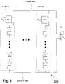
- the photovoltaic power system comprises a plurality of parallel-connected photovoltaic strings 316 (e.g. 316a, 316n etc.).
- a photovoltaic string 316 includes a plurality of series-connected photovoltaic panels 101 (e.g. solar cells, solar panels), which may be referred to as photovoltaic (PV) modules 101.
- PV photovoltaic
- other types of power sources may be used, such as batteries, storage devices, power producing device, and the like.
- a string 316 may be or may be similar to the string 315. According to some embodiments, due to the strings having different locations, each string (and the modules within a string) may receive a different amount of sunlight, which may cause one string to produce a different amount of power from another string. Furthermore, the serial connection between the modules within each string may lead to each string having a different voltage between the two ends of the string.
- a string compensation circuit configured to adapt the string voltage to allow parallel coupling.
- the input of a compensation circuit 307 e.g. 307-1, 307-n etc.
- a compensation device 307 or compensator 307 is coupled to an external power source Vs (e.g. Vs_a, Vs_b etc.).
- Vs e.g. Vs_a, Vs_b etc.
- the external power source will be detailed with reference to Fig.10 .
- the external power source may be implemented in various ways.
- the external power source may be an alternating-current (AC) source or a direct-current (DC) source.
- power source Vs may supply power produced by one or more PV modules in system 100.
- Compensator 307 may be configured in various ways. In an example not covered by the invention, if power source Vs outputs AC voltage, compensator 307 may include an AC-to-DC converter. In another example, if power source Vs outputs DC voltage, compensator 307 may include a DC-to-DC converter. In some embodiments, which are not according to the invention, compensator 307 may output a positive voltage, allowing the strings comprising system 100 to feature a common voltage equal to or higher than the highest string voltage without use of compensator units. According to the invention, compensator 307 includes a polarity adjustment circuit, configured to output a DC voltage of either positive or negative polarity, which allows system 100 to feature a common string voltage of arbitrary magnitude.
- each string 316 may be configured to operate at a voltage level optimal for generating maximum power, with one or more compensators 307 (e.g. 307-1, 307-n) configured to adjust the voltage between the ground bus (or other bus not necessarily at ground) and the DC bus to a uniform value for one or more or all strings in the power system.
- the combined voltage of the photovoltaic modules comprising the string may be configured to maximize the power output by the modules, with compensator 307-1 increasing or decreasing the total string voltage to match the system common voltage level.
- Compensator 307 may output a voltage configured to bring the total voltage between the ground and power buses to a desirable operating point, and compensator 307 may output a current which is equal to the string current at the desirable operating point.
- the power processed by each compensation circuit may be small compared to the power produced by each string, which may result in a cheap and efficient method of producing maximum power by allowing a string to operate at the string's optimal voltage without requiring electronics rated to process the full-string power.
- a ground bus (or other bus not necessarily at ground) and DC bus may be coupled to the ends of each PV string, and the ground bus (or other bus not necessarily at ground) and DC bus may be input to inverter 301 or some other device (e.g., storage device, DC/DC power converter, etc.), which may be configured to output AC power to a load, such as a grid, a home, or energy storage devices.
- a load such as a grid, a home, or energy storage devices.
- a compensation device 307 includes an isolated power converter, such as a Flyback DC-DC converter or a Forward DC/DC converter.
- a Flyback converter is considered and described, while other types of isolated converters may be used in exemplary embodiments.
- Flyback converter 213 may feature positive and negative input terminals (Vin+ and Vin-, respectively), and positive and negative output terminals (Vout+ and Vout-, respectively).
- the inputs may be electrically isolated from the outputs by use of transformer T3 formed by magnetically coupling windings L1 and L2.
- a Flyback converter can be considered an "isolated converter", i.e. a converter in which the input terminals are electrically isolated from the output terminals.
- the polarity of the Flyback output voltage may be configured by the polarity of winding L2. If L1 and L2 are wound with the same polarity, the voltage output by the converter will be inverted (i.e. of opposite polarity than the input voltage). If the polarity of winding L1 and the polarity of the winding L2 are different, the output voltage will be non-inverted (i.e. of the same polarity as the input). In converter 213, the windings L1 and L2 have opposite polarities, so converter 213 might not be inverting.
- Switches Q1 and Q2 may be switched in a complementary manner (i.e. when Q1 is ON, Q2 is OFF, and vice-versa), and may be used to regulate the output DC voltage.
- switch Q2 may be replaced by a diode.
- the magnitude of the output voltage may depend on the windings ratio between windings L1 and L2, and on the duty cycle of switch Q1.
- the output voltage magnitude may be higher or lower than the input voltage magnitude.
- the switching may be controlled by a control unit such as a microprocessor, ASIC, FPGA or similar suitable control device (not explicitly depicted).
- Capacitors Ci and Co may stabilize the input and output voltages, respectively.
- an isolated converter may be advantageous because the output voltage may be "floating" with regard to the input voltage, and by coupling the outputs serially with a photovoltaic string, the string voltage can be modified by the converter output without regard for the relative voltage input to the compensation circuit.
- a compensation circuit 307 may include an inverting Flyback converter, such as converter 212.
- Converter 212 may include the same functional components as those shown in converter 213, operating in the same way, with the difference between converter 213 and 212 being in the polarity of the windings.
- windings L1 and L2 are of the same polarity, resulting in a reversal of the polarity of the output voltage; the "upper" output terminal is the negative terminal Vout-, and the "lower” output terminal is the positive terminal Vout+.
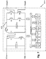
- Bipolar compensator 307e includes an isolated DC/DC converter 620 such as the Flyback converter discussed herein.
- the bipolar compensator further includes a polarity adjustment circuit such as a plurality of switches Q3, Q4, Q5, Q6 configured in a "full-bridge" topology, and coupled in parallel with the DC/DC converter 620 output.
- the compensator output voltage may have the magnitude of the DC/DC converter output stage, with the opposite polarity.
- Switches Q3, Q4, Q5 and Q6 may be controlled by the same controller that controls switches Q1 and Q2, or by a different controller.
- a bipolar compensation unit can increase a string voltage by outputting a positive DC voltage, or can decrease the string voltage by outputting a negative DC voltage.
- Compensation circuit 307e may be coupled to communication devices configured to communicate with one another and/or one or more system management units, such as a master system control device.
- compensator 307e may include Maximum Power Point Tracking (MPPT) device 398, which may be configured to extract maximum power from a PV module that may be coupled to the power device.
- the DC/DC conversion controller may include MPPT functionality.
- Compensator 307e may further comprise control device 371, which may be a microprocessor, Digital Signal Processor (DSP), ASIC and/or an FPGA.
- DSP Digital Signal Processor
- Control device 371 may control and/or communicate with other elements of compensator 307e over common bus 390 (or one or more other bus components).
- compensator 307e may include circuitry and/or sensors 380 configured to measure parameters on or near a photovoltaic module and/or compensator components. These parameters may include the voltage and/or current output by the module, the power output by the module, the irradiance received by the module, and/or the temperature on or near the module.
- compensator 307e may include communication device 350, which may be configured to transmit and/or receive data and/or commands from other devices. Communication device 350 may communicate using Power Line Communication (PLC) technology, or wireless technologies such as ZigBee, Wi-Fi, Bluetooth, cellular communication or other wireless methods.
- PLC Power Line Communication
- compensator 307e may include safety devices 360 (e.g., fuses, circuit breakers, and/or Residual Current Detectors).
- Compensator 307e may further include an auxiliary power circuit 394, which may be configured to supply various voltage and/or current levels to power the various compensator components.
- the various components of compensator 307e may communicate and/or share data over common bus 390 (or one or more other bus components).
- Bipolar compensator 307f may include a rectifier circuit 610 coupled (e.g., in parallel) to a polarity adjustment circuit 630.
- the polarity adjustment circuit 630 may be composed of switches Q1, Q2, Q3 and Q4 configured in a "full-bridge" arrangement.
- Rectifier circuit 610 may be configured to convert an AC input to a DC output, and may be implemented using, for example, four diodes in a "rectifying full bridge” arrangement.
- Bipolar compensator 307f may receive an AC output from an external power source (e.g., from the power grid or from a DC/AC inverter).
- Rectifier circuit 610 may further include a DC/DC conversion stage, and may be controlled to output a DC voltage of any magnitude.
- Switches Q1, Q2, Q3, and Q4 may be configured to control to polarity of the output DC voltage. When Q1 and Q4 are ON and Q2, Q3 are OFF, the compensator DC output may be positive, and when Q1 and Q4 are OFF and Q2, Q3 are ON, the compensator DC output may be negative.
- Compensator 307f may include communication, safety, sensor, MPPT and/or auxiliary power devices similar to the circuits discussed with regard to compensator 307e, but not explicitly depicted in Fig. 8 for the sake of brevity.
- Optimized photovoltaic power system 200 may be variously configured.
- the photovoltaic power system may comprise a plurality of parallel-connected photovoltaic strings 317 (e.g. 317a, 317n etc.).
- a photovoltaic string 317 may include a plurality of series-connected photovoltaic modules 101 (e.g. solar cells, solar panels).
- a string 317 may be or may be similar to the string 315.
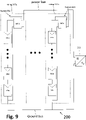
- the parallel string may be coupled between a ground bus (or other bus not necessarily at ground) and a DC bus, with the input of each bus connected to inverter 301, which may be configured to output AC power to the grid, home, or energy storage devices. Due to the strings 317 having different locations, each string 317 (and the modules within a string 317) may receive a different amount of sunlight and produce a different amount of power. Furthermore, the serial connection between the modules within each string 317 may lead to each string having a different voltage between its two ends. For different strings to be coupled in parallel, one or more or all of the strings in system 200 may be coupled to a string compensation circuit, which may be configured to adapt the string voltage to allow parallel coupling.
- a compensation circuit 307 e.g.
- each compensator 307 may receive a DC input from one or more PV modules comprising a PV string. As shown in Fig. 9 , each compensator 307 may be coupled to an entire PV string. For example, the negative input (Vin-) of compensator 307-1 may be coupled to the ground bus (or other bus not necessarily at ground), and the positive input (Vin+) may be coupled to the positive output terminal of PV module 101m, which may be the last module in the serially connected string of modules 101a..101m.
- Compensator 307 may include an isolated DC/DC converter such as one of the Flyback converters depicted in Figs. 6A and 6B .
- two current paths between the compensator input terminal (s) and output terminal(s) may be formed.
- current may be able to flow from the compensator input directly to the output via bypass B1a, and current may flow into the compensator at the input terminals, and flow out of the compensator at the outputs after being processed by the compensator.
- the power injected into the inputs of the compensator 307-1 may be significantly reduced, and the cost of implementing may be reduced as well. For instance, if a large voltage (e.g.
- a full-string voltage is input to a compensator 307, by directing a small portion of the current to the compensator inputs and a larger portion directly to the output (via a bypass path), the compensator may process a reduced amount of power, and the components needed for realization of the compensator may be correspondingly smaller and cheaper.
- Optimized photovoltaic power system 300 comprises a plurality of photovoltaic strings 318 (e.g. 318a, 318n etc.) coupled in parallel between ground and DC buses.
- a ground bus (or other bus not necessarily at ground) and DC bus are coupled to the ends of each PV string 318, and the ground bus (or other bus not necessarily at ground) and DC bus may be input to inverter 301, which may be configured to output AC power to a load, such as a grid, a home, and/or energy storage devices.
- the strings 318 feature a plurality of serially-connected photovoltaic modules 101 (e.g.
- a string 318 may be or may be similar to the string 315.
- the two inputs of a string compensation circuit 307 (e.g. 307-1) are coupled in parallel to a photovoltaic module (e.g. 101m), and a portion of the power produced by PV module may be input to the compensator 307. The rest of the power is transferred directly to the compensator 307 output via a bypass path.
- the compensation circuit 307 may process the input power and output a voltage to bring to the total string voltage to the desired common voltage between the ground and power buses, while allowing the plurality of series-connected PV modules in the string to operate at a voltage yielding maximum power output. Similarly to other embodiments disclosed herein, processing a portion of the string power may allow components to be smaller and cheaper, and may result in enhanced system efficiency.
- Fig. 11A illustrates the current flowing in different branches of a photovoltaic module 101 coupled to a compensator 307g according to exemplary embodiments.
- the module 101 may be part of a string of panels 101, such as shown in other figures discussed herein.
- a unipolar compensator e.g., might not include a polarity adjustment circuit
- a non-inverting Flyback converter is used.
- the current-flow analysis is similar for a bipolar compensator such as compensator 307e, and either a unipolar compensator or a bipolar compensator may be used in exemplary systems and scenarios, such as the systems and scenarios described herein.
- Unipolar compensator 307g may include a Flyback converter featuring a pair of input terminals, Vin+ and Vin-, and a pair of output terminals, Vout+ and Vout-.
- additional components e.g. communication, safety, control and/or monitoring devices etc. as depicted with regard to compensator 307e) are not explicitly depicted.
- the compensator may include capacitor Ci coupled between the inputs, and capacitor Co coupled between the outputs.
- Switches Q1 and Q2 e.g. MOSFETs
- Q1 may be coupled between the negative input terminal Vin- and winding L1
- Q2 may be coupled between the negative output terminal Vout- and winding L2.
- the windings may be magnetically coupled to one another by a magnetic core.
- PV module 101 may be coupled to the inputs, and may input photovoltaic power to the compensation circuit.
- Q1 When Q1 is ON and Q2 is OFF (illustrated in Fig. 11A with an "X"), winding L1 may draw current from PV module 101 and the discharging capacitor Ci.
- the module current Ip may be divided into current portion Id which may be input to the compensator may charge L1, and into current portion Is which may bypass the compensator input and may flow through the output terminals, charging capacitor Co while flowing from Vout-to Vout+.
- Current Is may be the effective string (e.g., string 317a depicted in Fig. 9 ) current, and may flow into compensation circuit 307g via string conductor 631, and may continue to flow from Vout+ via string conductor 631.
- the power drawn by compensator 307g during this time is given by V ci ⁇ ( I p - I s ), which may be significantly lower than the power output by module 101, which is given by V ci ⁇ I p .
- V out+ V in + + V C o .
- V C o positive
- the output voltage may be higher than the input voltage.
- FIG. 11B illustrates the current flowing in different branches of a compensator 307g when Q1 is OFF (illustrated in Fig. 11B with an "X") and Q2 is ON.
- Photovoltaic module 101 may output a current Ip, which is divided into two portions. One portion, Is, bypasses the compensator inputs and flows directly to the negative output terminal Vout- via a bypass path. A second portion, Ici flows into the compensator to charge capacitor Ci.
- Winding L1 transfers stored energy via a shared magnetic core to winding L2, which discharges the energy by generating current IL2 which flows towards output Vout+.
- Capacitor Co discharges, adding the capacitor Co's discharge current Ico to IL2 form the string current Is.
- the power input to compensator 307g may be significantly lower than the power generated by the panel.
- the charging and discharging of capacitors Ci and Co may be configured to adjust output voltage Vout+ to a value which brings a photovoltaic string voltage to a desired common voltage.
- the compensator includes a polarity adjustment circuit (e.g., a full-bridge of switches), either output value may be obtained, according to how the polarity adjustment circuit is operated.
- a polarity adjustment circuit e.g., a full-bridge of switches
- Appropriate choice of windings ratio and duty-cycle may allow flexible and robust system management, while obtaining high efficiency and low-cost by the compensator processing a portion of the string or PV module output power.
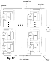
- Photovoltaic power system 400 may comprise a plurality of photovoltaic strings 319 (e.g. 319a, 319n etc.) coupled in parallel between a ground bus (or other bus not necessarily at ground) and a power bus.
- a photovoltaic string 319 may include a plurality of photovoltaic modules 101 (e.g. 101a, 101b, etc.) such as solar cells and/or solar panels.
- a string 319 may be or may be similar to the string 315.
- a plurality of power devices 700 e.g.
- a power device 700 may be the compensation circuit 307 discussed herein, may be similar to the compensation circuit 307 discussed herein, and/or may include one or more or all of the compensation circuit 307's components.
- the power device 700 may be similar to unipolar compensation circuit 307g or to bipolar compensation circuit 307e, featuring a Flyback DC/DC converter.
- a DC/AC microinverter may be utilized to output an AC voltage, with each microinverter's output coupled in series to generate an AC string voltage of comparable magnitude to grid voltage.
- the inputs of each power device may be coupled to the outputs of a PV module 101.
- multiple modules may be coupled in series and the resultant series coupled to an input of a power device 700.
- power devices may be coupled to some or to all of the modules in a string or a system.
- Each power device 700 may comprise a power conversion circuit configured to regulate the power drawn from its corresponding PV modules(s), by using techniques such as MPPT, "perturb and observe", impedance matching, and/or other methods of determining and tracking a maximum power point or a power point close to the maximum power point.
- the positive input terminal of one or more power device(s) 700 may be coupled to one of the output terminals, allowing current to flow directly to the device output without being processed by the power device, which may potentially result in efficiency advantages as explained herein. For example, if each module 101 in the system is coupled to a power device 700, the majority of each string's current may flow directly from power device inputs to the output with being processed by the device.
- the device 700 may still process a small portion of the system power, employing power conversion to ensure that each module is working near or at its maximum power point.
- Each power device 700 may receive a DC power input, and output an appropriate output.
- the output may be a DC voltage.
- a DC signal greater or smaller than the input voltage may be obtained.
- each power device 700 may be configured to output an AC signal.
- each power device 700 may output a time-varying DC signal such as a rectified sine wave, rectangular, or square wave.
- Each power device 700 may have one output coupled to the device 700's positive input terminal, and the device 700's other output coupled in series to the photovoltaic string
- a system power device 710 may be coupled between the ground and power buses.
- system power device 710 may include or be an inverter configured to convert a DC input (e.g., input from the one or more power devices 700) to an AC output to a load, such as a home or a grid.
- the system power device 710 may be a storage device, such as a battery or capacitor.
- the system power device 710 may be a DC/DC converter.
- device 710 may include safety, control, communication, monitoring and/or management devices, which may be coupled to one or more of the other components of system 400, such as a power device 700.
- Fig. 12 may depict a system of serially connected PV devices power 700
- embodiments may include other connection methods.
- a plurality of PV power devices may be coupled in parallel.
- this configuration may be functionally and/or electrically equivalent to a system such as system 400, wherein each string is of length one (i.e., each string contains one PV module coupled in parallel to one PV power device, with the power device inputs and outputs configured as in system 400).
- Some embodiments may be of hybrid serial-parallel nature.
- an exemplary photovoltaic string may include a plurality of pairs of PV modules, wherein each module in each pair is coupled to a power device in the manner disclosed herein (e.g., each power device may include an isolated converter with one of the converter's inputs coupled to one of the converter's outputs) the power devices are coupled in parallel, and a plurality of such pairs are coupled in series, forming a serial string coupled between the ground and power buses.
- additional power sources may be featured, such as batteries, wind turbines, fuel cells, etc. Many additional layouts, which make use of the novel features disclosed herein, may be implemented and are included in one or more exemplary embodiments.
- Integrated block 50 may include PV module 101, which may be coupled to power converter 204.
- the converter 204 may be and/or include one or more components or devices described herein.
- the converter 204 may be a DC/DC or DC/AC converter, configured to receive a DC input from module 101 and output a DC, time-varying-DC, or AC signal.
- Power converter 204 may include an isolated converter such as a Flyback or Forward converter (such as described herein), and in some embodiments may include a polarity adjustment circuit (such as described herein).
- Integrated block 50 may include circuits and devices discussed herein (e.g.
- Integrated block 50 may be packaged and deployed as a single unit. In some embodiments, a single integrated block 50 may be deployed in one or more of the PV strings to supply voltage-compensation functionality. In some embodiments, entire PV strings may comprise serially coupled integrated blocks. In some embodiments, integrated block 50 may feature a few terminals (e.g., two terminals), which may allow for fast and simple system installation, while obtaining the benefits of a sophisticated electronic system with minimal installation complexity. In some embodiments, integrated block 50 may be embedded onto a roof shingle, with electrical contacts placed to create serial electric connection between integrated blocks when shingles are placed next to one another.
- PV power device 700a may include some or all of the components of integrated block 50, and may be similarly arranged, with the exclusion of a power-generating PV module.
- Power device 700a may include power converter 206.
- the converter 206 may be and/or include one or more components or devices described herein.
- the converter 206 may be a DC/DC or DC/AC converter, configured to receive a DC input from module 101 and output a DC, time-varying-DC, or AC signal.
- Power converter 206 may include an isolated converter such as a Flyback or Forward converter (such as described herein), and in some embodiments may include a polarity adjustment circuit (such as described herein).
- the power converter 204 and/or the power converter 206 may be the same as or may be similar to one another. According to some aspects, the power converter 204 and/or the power converter 206 may be the same as or similar to the compensation device 307 and/or to the power device 700. According to some aspects, the compensation device 307 and/or the power device 700 may be the same as or similar to the power converter 204 and/or the power converter 206.
- power device 700a may include circuits and devices discussed herein, such as circuits and devices discussed with regard to other embodiments and figures (e.g. bipolar compensator 307e and/or integrated block 50) such as communication device 350, sensor(s) 380, controller 371, MPPT device 398, safety device(s) 360, auxiliary power circuit 394, and/or common bus 390 (or one or more other bus components).
- PV power device 700a may include a pair of input terminals T1 and T2 configured to receive DC power from, for example, a photovoltaic module and/or another power source.
- the power device may include terminals T3 and T4, configured to be serially coupled to similar power devices.
- T3 and T4 are coupled at the time of manufacturing to conductors leading to similar power devices.
- the plurality of power devices 6 can be quickly and efficiently deployed during installation. For example, if two adjacent photovoltaic modules are placed such that their junction boxes are 1.5 meters apart, each pair of PV power devices 6 may be coupled by a conductor approximately 1.5 meters long, with a plurality of such coupled devices forming a "chain" that can be rapidly coupled to all the PV modules in the string.
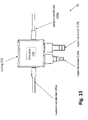
- PV power device 70 may comprise casing 231.
- Circuitry 230 e.g., which may be any of the circuitry described or referred to herein, such as device 307, device 700, device 50, power converters, etc.
- casing 231 may include all or some of the power devices described with regard to compensation circuits and/or PV power devices, such as a DC/DC and/or DC/AC converter, communication device(s), sensor(s), controller(s), MPPT device(s), safety device(s), auxiliary power circuit(s) and/or common bus(es).
- casing 231 might not comprise a full enclosure.
- casing 231 may comprise a lid-like surface designed to be placed on a PV module junction box and mechanically connected to the junction box, such that circuitry 230 mounted on the lid is electronically coupled to the PV module when the lid is fastened to the junction box.
- PV power device 70 may include input terminals 210a and 210b configured to receive power from one or more photovoltaic modules and transfer it to circuitry 230, and a pair of output conductors 220a and 220b configured to output power to the photovoltaic string.
- one of the input terminals may be internally (i.e.
- the output conductors may be coupled to additional PV power devices similar to device 70, forming a chain of power devices, and may be of appropriate length to allow adjacent devices in the device chain to be coupled to adjacent modules in a photovoltaic installation.
- a plurality of photovoltaic devices 8 may be coupled by output conductors 220, forming a chain of devices 8.
- Each PV device 8 may be any of, of similar function of, and/or of similar structure of one or more of the devices disclosed herein, such as device 307, device 700, device 50, power converters, etc.
- Output conductors 220 may each be of appropriate length to allow adjacent devices 8 in the device to be coupled to adjacent modules in a photovoltaic installation.
- the chain of devices may be efficiently and effectively stored.
- the chain of devices 8 and output conductors 220 may be wound around storage device 401, which may resemble a cabling reel, allowing the storage device to be rolled along a plurality of PV modules while coupling devices from the chain to the modules.
Landscapes
- Engineering & Computer Science (AREA)
- Power Engineering (AREA)
- Electromagnetism (AREA)
- Sustainable Energy (AREA)
- Sustainable Development (AREA)
- Physics & Mathematics (AREA)
- Life Sciences & Earth Sciences (AREA)
- General Physics & Mathematics (AREA)
- Radar, Positioning & Navigation (AREA)
- Automation & Control Theory (AREA)
- Control Of Electrical Variables (AREA)
- Supply And Distribution Of Alternating Current (AREA)
- Charge And Discharge Circuits For Batteries Or The Like (AREA)
Description
- Photovoltaic (PV) power devices can be used to improve the performance and to reduce the cost of power generation systems including photovoltaic panels. Photovoltaic power devices can be variously configured. The cost of some power devices may be proportional to the amount of electrical power they process. Thus, significant savings can be realized by designing systems to optimize output power while processing a small portion of the system power.
- Accordingly, there is a need for designing power device system with increased efficiency while decreasing the operating costs associated with such as system.
- The exemplary features presented relate to a photovoltaic power harvesting system including multiple photovoltaic strings and, more particularly to system and method for maximizing power in each photovoltaic string.
- Reference is made to
Fig. 1 which shows a photovoltaicpower harvesting system 10 according to conventional art. Aphotovoltaic string 109 includes a series connection ofphotovoltaic panels 101.Photovoltaic strings 109 may be connected in parallel to give a parallel direct current (DC) power output. The parallel DC power output connects to the input of a direct current (DC) to alternating current (AC)inverter 103. The AC power output ofinverter 103 connects across anAC load 105.AC load 105 may be an AC load such as an AC motor or may be an electrical power grid. - By way of a simplified numerical example, three
strings 109 may be used with aninverter 103. If twostrings 109 are equally irradiated such that each string operates with a string voltage of 600 volts (V) and string current of 10 amperes (A); each of the two strings generates (10 A · 600 V) 6 kilowatts (kW). It is also assumed that the two equallyirradiated strings 109 may be operating at maximum power. - If however, one
string 109 is partially shaded or if one ormore panels 101 is under performing, there may still be a string voltage of 600V as set by the other two equallyirradiated strings 109, however, the string current in the one under performingstring 109 may only be only 6 amperes. The under performingstring 109 is not operating at maximum power point. For instance, it may be that the under performingstring 109 has a maximum power point of 550 volts for a current of 10 amperes. In this situation, the power lost by the under performingstring 109 is 1.9kW (550V·10A - 600V·6A). The under performingstring 109, therefore, produces 3.6kW (600V·6A). Overall power harvested fromsystem 10 is, therefore 15.6kW (3.6kW + 2 · 6kW). - Reference is now made to
Fig. 2 which shows anotherpower harvesting system 20 according to conventional art, according to international patent application publicationWO2010002960 .System 20 is directed to reduce power losses compared to the losses ofsystem 10. Eachphotovoltaic string 109 includes a series connection ofphotovoltaic panels 101. Eachphotovoltaic string 109 is connected in parallel to an input of a DC-to-DC converter 205. The output ofconverter 205 connects to aDC bus 211. The DC voltage generated byphotovoltaic string 109 is converted byconverter 205 to the voltage ofDC bus 211. Eachphotovoltaic string 109 together with the respective DC-DC converter 205 forms aphotovoltaic string module 207. A number ofmodules 207 with outputs from respective DC-to-DC converters 205 may be connected in parallel toDC bus 211. The parallel combined outputs ofmodules 207 may be also connected to an input of a direct current (DC) to alternating current (AC) inverter 103 viaDC bus 211.Inverter 103 converts the combined DC power outputs ofmodules 207 to an alternating current power at an output ofinverter 103. The output ofinverter 103 connects toAC load 105. - Still referring to
Fig. 2 , using the same numerical example as in system 10 (Fig. 1 ), threemodules 207 may be used withinverter 103. Twostrings 109 may be equally irradiated such that each string of the two strings operates with a string voltage of 600 volts and string current of 10 amperes. Each of the two strings generates (10 amperes . 600 volts) or 6 kilowatts. If the oneremaining string 109 is under performing, there may be maximum power point for the under performingstring 109 of 550 volts and current of 10 amperes. Each DC-to-DC converter 205 may be configured to maximize power on each respective output to give 600 volts onDC bus 211. The two equallyirradiated modules 207 each produce 6 kW (10 amperes· 600 volts) and the under performingunit 207 produces 5.5 kW (10 amperes · 550 volts). Giving an overall power harvested fromsystem 20 of 17.5 kW. It can be seen thatsystem 20 offers an improvement of 1.9kW oversystem 10 in terms of minimized losses and increased power harvested. The improvement has been achieved through multiple DC-DC converters 205 which operate at wattage levels of around 6 kW. The high power DC-DC converters 205 in a power harvesting system may add to the cost of installation and maintenance of the power harvesting system and may present an overall decreased level of reliability for the power harvesting system because DC-DC converters 205 operate at high wattage levels. -
US2013/193765 discloses system comprising: a plurality of parallel-connected compensated photovoltaic strings, each compensated photovoltaic string including: a photovoltaic string having a series-connection of photovoltaic cells; and a voltage-compensation circuit having a voltage output connected in series with said photovoltaic string, wherein said voltage-compensation circuit includes an input connected to a source of power separate from power provided by the photovoltaic string, wherein the voltage-compensation circuit is configured to provide at the voltage output an adjustable compensation voltage in series with a voltage generated by said photovoltaic string such that a total voltage of the compensated photovoltaic string maintains a predetermined value. - HUIMIN ZHOU ET AL, "PV Balancers: Concept, Architectures, and Realization", IEEE TRANSACTIONS ON POWER ELECTRONICS, USA, vol. 30, no. 7, doi:10.1109/TPEL.2014.2343615, ISSN 0885-8993, pages 3479 - 3487, discloses PV balancers that are DC-DC converters, which are integrated into each module, and combined into a common DC bus configuration.
- HUIMIN ZHOU ET AL, "PV balancers: Concept, architectures, and realization", ENERGY CONVERSION CONGRESS AND EXPOSITION (ECCE), 2012 IEEE, IEEE, doi:10.1109/ECCE.2012.6342469, ISBN 978-1-4673-0802-1, pages 3749 - 3755, discloses PV balancers that are DC-DC converters, which are integrated into each module, and combined into a common DC bus configuration.
-
US2010/126550 discloses an apparatus that controls the power produced by a string of solar cells, enabling the string to operate at its maximum power point when connected to a bus that operates at an externally controlled voltage. The apparatus can also be used to increase or decrease the output power of a string to any desired operating point. -
US2015/364918 discloses a system for optimizing load current in a string of solar panels. A string of solar panels includes a microprocessor coupled to the string of solar panels. The system includes a first DC-to-DC converter comprising input terminals coupled to a load and output terminals coupled to each solar panel in the string of solar panels. The first DC-to-DC converter is operable to supply a compensatory power for compensating a drop in the peak current arising due to shading of one or more solar panels. Moreover, the system includes a second DC-to-DC converter coupled to the first DC-to-DC converter. The second DC-to-DC converter is operable as one of a voltage adder and a voltage subtractor to generate a compensatory voltage for compensating a drop in the load current arising due to panel mismatch among the string of solar panels. - The terms "monitoring", "sensing" and "measuring" are used herein interchangeably.
- The terms "power grid" and "mains grid" are used herein interchangeably and refer to a source of alternating current (AC) power provided by a power supply company.
- The term "converter" as used herein applies to DC-to-DC converters, AC-to-DC converters, DC-to-AC inverters, buck converters, boost converters, buck-boost converters, full-bridge converters and half-bridge converters or any other circuit for electrical power conversion/inversion known in the art.
- The term "DC load" as used herein applies to the DC inputs of converters, batteries, DC motors or DC generators.
- The term "AC load" as used herein applies to the AC inputs of converters, transformers, AC motors or AC generators.
- The present invention is defined in the appended claims.
- These and other features, aspects, and advantages of the present disclosure will become better understood with regard to the following description, claims, and drawings. The present disclosure is illustrated by way of example, and not limited by, the accompanying figures. A more complete understanding of the present disclosure and the advantages thereof may be acquired by referring to the following description in consideration of the accompanying drawings, in which like reference numbers indicate like features.
-
Fig. 1 shows a photovoltaic power harvesting system according to conventional art. -
Fig. 2 shows another photovoltaic power harvesting system according to conventional art. -
Fig. 3a shows a power harvesting system. -
Fig. 3b shows a power harvesting system. -
Fig. 3c shows more details of a voltage-compensation circuit shown inFigs. 3a and3b not forming part of the invention as such but useful for providing an understanding thereof. -
Fig. 3d shows an implementation of a voltage-compensation circuit shown inFigs. 3a and3b not forming part of the invention. -
Fig. 4 shows a method applied to the power harvesting systems shown inFigs. 3a and3b . -
Fig. 5 depicts a part schematic, part block-diagram of an exemplary power system. -
Figs. 6A-6B depict schematic diagrams of exemplary isolated power converters not forming part of the invention. -
Fig. 7 depicts a part schematic, part block-diagram of a compensation circuit featured in an exemplary embodiment of the invention. -
Fig. 8 depicts a part schematic, part block-diagram of a compensation circuit not forming part of the present invention as such but useful for providing an understanding thereof. -
Fig. 9 depicts a part schematic, part block-diagram of an exemplary power system not forming part of the invention as such but useful for providing an understanding thereof. -
Fig. 10 depicts a part schematic, part block-diagram of an exemplary power system according to exemplary embodiments of the invention. -
Figs. 11A-11B depict part schematic, part block-diagram illustrations of current flow through an exemplary compensation not forming part of the invention as such but useful for providing an understanding thereof. -
Fig. 12 depicts a part schematic, part block-diagram of an exemplary power system not forming part of the invention. -
Fig. 13 depicts a part schematic, part block-diagram of an integrated solar block not forming part of the invention. -
Fig. 14 depicts a part schematic, part block-diagram of an exemplary power device not forming part of the invention. -
Fig. 15 depicts a part schematic, part block-diagram of an exemplary power device not forming part of the invention. -
Fig. 16 depicts an illustrative diagram showing storage of exemplary power devices not forming part of the invention. - In the following description of various illustrative embodiments, reference is made to the accompanying drawings, which form a part hereof, and in which is shown, by way of illustration, various embodiments in which aspects of the disclosure may be practiced. It is to be understood that other embodiments may be utilized and structural and functional modifications may be made, without departing from the scope of the present disclosure.
- It should be noted, that although the discussion herein relates primarily to photovoltaic systems, the teachings disclosed herein may, by non-limiting example, alternatively be configured using other distributed power systems including (but not limited to) wind turbines, hydro turbines, fuel cells, storage systems such as battery, super-conducting flywheel, and capacitors, and mechanical devices including conventional and variable speed diesel engines, Stirling engines, gas turbines, and micro-turbines.
- By way of introduction, features of the present invention are directed towards maximizing output power from under-performing or partially shaded photovoltaic strings in a power harvesting system of parallel connected photovoltaic strings. The features may provide maximal overall power output of the system and reduced installation and maintenance cost of the system. The features may also provide increased reliability of the system, owing to lower power operating levels of switching converters added to each of the photovoltaic string compared with DC-
DC converters 205 used inconventional system 20. - Reference is now made to
Fig. 3a which shows apower harvesting system 30a according to a feature of the present invention. A number ofphotovoltaic panels 101 are connected in series to form aphotovoltaic string 109.String 109 is connected in series with a voltage-compensation circuit 307 to provide a compensatedstring 315. A source voltage (Vs) may be input to voltage-compensation circuit 307. A number of compensatedstrings 315 are connected together in parallel to give direct current (DC)power output 211. Apower sensor 370 operatively connected tocentral controller 313 measures the power onDC output 211.DC power output 211 is connected to an input of a DC to alternating current (AC)inverter 103.Inverter 103 converts the combinedDC power output 211 ofstrings 315 to an alternating current power at an output ofinverter 103. The output ofinverter 103 connects toAC load 105. Acentral controller 313 may be operatively attached to each voltage-compensation circuit 307 by bi-directional control and communication lines as shown, by wireless communication or by power line communications inDC bus 211.Central controller 313 may include a microprocessor with on-board memory and an interface which may include analogue to digital converters (ADCs) and digital to analogue converters (DACs). - Reference is now made to
Fig. 3b which shows apower harvesting system 30b according to another feature of the present invention.String 109 is connected in series with voltage-compensation circuit 307 to provide a compensatedstring 315. A source voltage (Vs) is input to voltage-compensation circuit 307. A number of compensatedstrings 315 are connected together in parallel to give direct current (DC)power output 211.DC power output 211 is connected to an input of a DC to alternating current (AC)inverter 103.Inverter 103 converts the combinedDC power output 211 ofstrings 315 to an alternating current power at an output ofinverter 103. The output ofinverter 103 connects toAC load 105.System 30a is the same assystem 30b except thatsystem 30b does not havecentral controller 313. Instead, monitoring and control insystem 30b is performed by eachcircuit 307, which may include a microprocessor with on-board memory and an interface which may include analogue to digital converters (ADCs) and digital to analogue converters (DACs). Eachcircuit 307 is operatively attached tosensors Sensors photovoltaic string 109 as well as current instring 109. Alternatively,sensors string 315 and current instring 315. Alternatively,sensors circuit 307 as well as current through thecircuit 307. - Reference is now made to
Fig. 3c which shows more details of voltage-compensation circuit 307 shown inFigures 3a and3b , which are not part of the invention. Voltage-compensation circuit 307 may be implemented using a direct current (DC) to DC converter 307a. DC-to-DC converter 307a may be a buck circuit, a boost circuit, a buck + boost circuit or switched-mode power supply (SMPS). The output of DC-to-DC converter 307 is connected in series withinstring 315 to add compensation voltage (Vc) tostring 315. The DC source voltage input (Vs) to DC-toDC converter 307 may be provided from the combined DC output ofstrings 315, or strings 109. Alternatively, DC source voltage input (Vs) may be provided by a micro-inverter converting AC from the mains grid or another independent source of DC power such as a battery or DC generator.Circuit 307 as shown inFig. 3c , is a conventional buck-boost DC- to-DC converter circuit which has an input voltage Vs with an input capacitor C1 connected in parallel across Vs. Two switches may be implemented as field effect transistors (FET) with integral diodes: a high side buck switch Q1 and a low side buck switch Q2 connected in series by connecting the source of Q1 to the drain of Q2. The drain of Q1 and the source of Q2 may be connected parallel across the input capacitor C1. A node A is formed between switches Q1 and Q2 to which one end of an inductor L is connected. The other end of inductor L is connected to the boost circuit of buck-boost DC-to-DC converter 307 at a node B. Node B connects two switches implemented as field effect transistors (FET): a high side boost switch Q4 and a low side boost switch Q3 together in series where the source of Q4 connects to the drain of Q3 to form node B. The drain of Q4 and the source of Q3 connect across an output capacitor C2 to produce the output voltage VC of buck-boost DC-to-DC converter 307. - Reference is now made to
Fig. 3d which shows an implementation ofcircuit 307 shown inFigures 3a and3b , which is not part of the invention.Voltage compensation circuit 307 may be implemented using an alternating current (AC) to DC inverter. The AC toDC inverter 307b may be a type of switched mode power supply (SMPS). When voltage-compensation circuit 307 is an AC toDC converter 307b, the DC output of the AC to DC converter is connected in series within astring 315. The AC input (Vs) to the AC to DC converter may be provided from the mains grid, from the AC output ofinverter 103 or by another independent source of AC power. - Reference is now made to
Fig. 4 which shows amethod 400 which may be applied topower harvesting system 30b shown inFig. 3b , according to a feature of the present invention. Instep 402, an output voltage (Vc) ofcircuit 307 is wired in series with a series-connection ofpanels 101 to form compensatedstring 315. The input voltage (Vs) tocircuit 307 may be from direct current (DC)output 211, the alternating current (AC) output ofinverter 103 or a separate independent AC or DC electric supply. Several compensatedstrings 315 outputs may then be connected in parallel and further connected to the input of aninverter 103 as shown inFig. 3b . - In
step 404, a circuit parameter of each parallelconnected string 315 is monitored in the case ofsystem 30b. The circuit parameter may be the current flowing in astring 315, the voltage across astring 315, the voltage of aphotovoltaic string 109 and/or the voltage (Vc) across acircuit 307. The current and voltages in astring 315 may be used to determine the power (P) in astring 315 or aphotovoltaic string 109 by virtue of power being equal to voltage (V) multiplied by current (I). - In
decision block 406, a control algorithm stored in acircuit 307 adjusts compensation voltage VC to maximize output power ofstring 315. In step 408, a compensation voltage Vc forstrings 315 is configured based on the result of the control algorithm performed insteps strings 315 in step 408 may be a positive or a negative voltage polarity with respect to the voltage polarity of astring 109. Instep 410, the compensation voltage Vc is added tostring 315. In the case of the positive voltage for Vc, the voltage of astring 315 may be increased in step 408. In the case of the negative voltage for Vc, the voltage ofstring 315 may be decreased in step 408. - Reference is still being made to
Fig. 4 .Method 400 may also be applied tosystem 30a (Fig. 3a ) which usescentral controller 313. In the case ofsystem 30a, instep 404 central controller monitors or calculates a net total power fromsystem 30a. The net total power fromsystem 30a is equal to the power produced bystrings 109 subtracted from the power added bycompensation circuits 307. - When the voltage (Vs) and hence power to the input of
circuit 307 is derived fromDC bus 211 or the output ofinverter 103 to give compensated voltage (Vc). The net total power fromsystem 30a may be derived directly by monitoring (step 404) power onDC bus 211. - When the voltage (Vs) and hence power to the input of
circuit 307 is derived from an independent DC source or AC source such as a mains supply to give compensated voltage (Vc). The net total power fromsystem 30a may be derived by subtracting power monitored on DC Bus 211 (step 404) from the power added bycompensation circuits 307. - In
decision block 406, compensation voltages Vc of allstrings 315 may be adjusted to maximize the net total power fromsystem 30a. In step 408, a compensation voltage Vc for astring 315 is configured based on the result of the control algorithm performed insteps step 410, the compensation voltage Vc is added to astring 315. - During a sustained use of
systems connected panels 101 in astring 315 may change, some panels may become faulty and/or operate in a current bypass mode or panels may be replaced with ones that have different electrical characteristics. Under these circumstances, the control algorithm maintainsstrings 315 at their maximum power point (MPP) by adding compensation voltage to eachstring 315 to maintain maximum power from eachstring 315. When allstrings 109 are found to be operating at maximum power output level and maximum power point, no voltage compensation Vc may be required and voltage compensation Vc added tostring 315 is at or near zero volts. - With respect to both
systems steps string 315, the minimum compensation voltage Vc. Subtracting the minimum compensation voltage Vc, may prevent a drift in the compensation voltages (Vc) going too high for no reason. Alternatively, it may be possible to tie the compensation voltages (Vc) to a level that will optimize the overall voltage ofstrings 315 to be optimal for the input ofinverter 103, thereby increasing the conversion efficiency ofinverter 103. - The present features with respect to
method 400 andsystems Fig. 2 ) by way of the same numerical example, where three compensatedstrings 315 are used. It may be assumed just for the purpose of the numerical example that the three compensatedstrings 315 are compensated bycircuit 307 which may be an AC to DC converter powered from the grid. Therefore,circuit 307 receives and converts voltage (Vs) and hence power from the electrical grid. If twostrings 109 are equally irradiated such that each string operates with astring 109 voltage of 600 volts and string current of 10 amperes, each of the two strings generates (10 amperes · 600 volts) 6 kilowatts. If one under-performingstring 109 is partially shaded or if apanel 101 is removed or bypassed, there may be a string voltage of 550 Volts and current of 10 amperes, which means (10 amperes · 550 volts) 5.5 kilowatts may be generated by the under-performingstring 109. The maximum power 5.5 kilowatts may be generated by the under-performingstring 109 only if the under-performingstring 109 can be operated at maximum power point (MPP). - Voltage-
compensation circuit 307 of the under-performingstring 109 may be configured (step 408) bycontroller 313 to add 50 volts (Vc) in series with under-performingstring 109 while maintaining the current of 10 amperes (step 410). Adding 50 volts by use of voltage-compensation circuit 307, maintainsstring 315 voltage at 600 volts also for under-performingstring 109. Increasing the voltage of thestring 315, allows the one under-performingstring 109 to operate at MPP and also requires an extra (10 amperes · 50 volts) 500 Watts when compared to the 6 kilowatts in each of the other twostrings 315. The overall power output ofsystem strings 109 providing 12 kilowatts (2 · 6 kilowatts), the under-performing compensatedstring 109 providing 5.5 kilowatts and the grid providing 500 watts (50 volts · 10 amperes) viacircuit 307. The power provided from the 3strings 315 may be therefore, the same assystem 20 at 17.5 kilowatts (2 · 6 kilowatts + 5.5 kilowatts). - The benefit of systems 30 compared with
system 20 is that 500W-1kW switching converters 307 may be required compared with 6-10kW switching converters used insystem 20. The difference in power rating may represent a huge improvement in cost and reliability of systems 30 compared withsystem 20. - Referring still to
Fig. 4 , themethod 400 and/or one or more steps set forth in themethod 400 may be performed by and/or for any of the systems devices, and/or components discussed herein, such as described in relation toFigs. 1-3 and toFigs. 5-16 , which are described below in greater detail. - Reference is now made to
Fig. 5 , which depicts a photovoltaic installation according to exemplary embodiments. Optimizedphotovoltaic power system 100 may be variously configured. In one embodiment, the photovoltaic power system comprises a plurality of parallel-connected photovoltaic strings 316 (e.g. 316a, 316n etc.). A photovoltaic string 316 includes a plurality of series-connected photovoltaic panels 101 (e.g. solar cells, solar panels), which may be referred to as photovoltaic (PV)modules 101. According to some aspects not covered by the present invention, other types of power sources may be used, such as batteries, storage devices, power producing device, and the like. According to some aspects, a string 316 may be or may be similar to thestring 315. According to some embodiments, due to the strings having different locations, each string (and the modules within a string) may receive a different amount of sunlight, which may cause one string to produce a different amount of power from another string. Furthermore, the serial connection between the modules within each string may lead to each string having a different voltage between the two ends of the string. - For different strings to be coupled in parallel, one or more or all of the strings in
system 100 are coupled to a string compensation circuit, configured to adapt the string voltage to allow parallel coupling. The input of a compensation circuit 307 (e.g. 307-1, 307-n etc.), sometimes referred to herein as acompensation device 307 orcompensator 307, is coupled to an external power source Vs (e.g. Vs_a, Vs_b etc.). In the invention, the external power source will be detailed with reference toFig.10 . In other examples, which are not part of the invention, the external power source may be implemented in various ways. For example, the external power source may be an alternating-current (AC) source or a direct-current (DC) source. In other examples, which are not part of the invention, power source Vs may supply power produced by one or more PV modules insystem 100. -
Compensator 307 may be configured in various ways. In an example not covered by the invention, if power source Vs outputs AC voltage,compensator 307 may include an AC-to-DC converter. In another example, if power source Vs outputs DC voltage,compensator 307 may include a DC-to-DC converter. In some embodiments, which are not according to the invention,compensator 307 may output a positive voltage, allowing thestrings comprising system 100 to feature a common voltage equal to or higher than the highest string voltage without use of compensator units. According to the invention,compensator 307 includes a polarity adjustment circuit, configured to output a DC voltage of either positive or negative polarity, which allowssystem 100 to feature a common string voltage of arbitrary magnitude. In this manner, each string 316 may be configured to operate at a voltage level optimal for generating maximum power, with one or more compensators 307 (e.g. 307-1, 307-n) configured to adjust the voltage between the ground bus (or other bus not necessarily at ground) and the DC bus to a uniform value for one or more or all strings in the power system. For example, instring 316a, the combined voltage of the photovoltaic modules comprising the string (101a, 101b... 101m) may be configured to maximize the power output by the modules, with compensator 307-1 increasing or decreasing the total string voltage to match the system common voltage level.Compensator 307 may output a voltage configured to bring the total voltage between the ground and power buses to a desirable operating point, andcompensator 307 may output a current which is equal to the string current at the desirable operating point. In some embodiments, the power processed by each compensation circuit may be small compared to the power produced by each string, which may result in a cheap and efficient method of producing maximum power by allowing a string to operate at the string's optimal voltage without requiring electronics rated to process the full-string power. A ground bus (or other bus not necessarily at ground) and DC bus may be coupled to the ends of each PV string, and the ground bus (or other bus not necessarily at ground) and DC bus may be input toinverter 301 or some other device (e.g., storage device, DC/DC power converter, etc.), which may be configured to output AC power to a load, such as a grid, a home, or energy storage devices. - Reference is now made to
Fig. 6A , which shows one exemplary implementation of a string compensation circuit/device 307c, according to some embodiments. Acompensation device 307 includes an isolated power converter, such as a Flyback DC-DC converter or a Forward DC/DC converter. For the purpose of this example, a Flyback converter is considered and described, while other types of isolated converters may be used in exemplary embodiments.Flyback converter 213 may feature positive and negative input terminals (Vin+ and Vin-, respectively), and positive and negative output terminals (Vout+ and Vout-, respectively). The inputs may be electrically isolated from the outputs by use of transformer T3 formed by magnetically coupling windings L1 and L2. For this reason, a Flyback converter can be considered an "isolated converter", i.e. a converter in which the input terminals are electrically isolated from the output terminals. The polarity of the Flyback output voltage may be configured by the polarity of winding L2. If L1 and L2 are wound with the same polarity, the voltage output by the converter will be inverted (i.e. of opposite polarity than the input voltage). If the polarity of winding L1 and the polarity of the winding L2 are different, the output voltage will be non-inverted (i.e. of the same polarity as the input). Inconverter 213, the windings L1 and L2 have opposite polarities, soconverter 213 might not be inverting. Switches Q1 and Q2 (e.g. MOSFETs, etc.) may be switched in a complementary manner (i.e. when Q1 is ON, Q2 is OFF, and vice-versa), and may be used to regulate the output DC voltage. In some embodiments, switch Q2 may be replaced by a diode. The magnitude of the output voltage may depend on the windings ratio between windings L1 and L2, and on the duty cycle of switch Q1. The output voltage magnitude may be higher or lower than the input voltage magnitude. The switching may be controlled by a control unit such as a microprocessor, ASIC, FPGA or similar suitable control device (not explicitly depicted). Capacitors Ci and Co may stabilize the input and output voltages, respectively. Use of an isolated converter may be advantageous because the output voltage may be "floating" with regard to the input voltage, and by coupling the outputs serially with a photovoltaic string, the string voltage can be modified by the converter output without regard for the relative voltage input to the compensation circuit. - Reference is now made to
Fig. 6B , which shows an exemplary implementation of astring compensation circuit 307d/string compensation device 307d, according to some embodiments. Acompensation circuit 307 may include an inverting Flyback converter, such asconverter 212.Converter 212 may include the same functional components as those shown inconverter 213, operating in the same way, with the difference betweenconverter converter 212, windings L1 and L2 are of the same polarity, resulting in a reversal of the polarity of the output voltage; the "upper" output terminal is the negative terminal Vout-, and the "lower" output terminal is the positive terminal Vout+. - Reference is now made to
Fig. 7 , which depicts one example of acompensation circuit 307, which is shown asbipolar compensation circuit 307e, according to an exemplary embodiment. While various examples ofcompensation circuits 307 may be described and/or referred to herein with respect to a figure or embodiment, any disclosedcompensation circuit 307 may be implemented in any disclosed or described example or embodiment.Bipolar compensator 307e includes an isolated DC/DC converter 620 such as the Flyback converter discussed herein. The bipolar compensator further includes a polarity adjustment circuit such as a plurality of switches Q3, Q4, Q5, Q6 configured in a "full-bridge" topology, and coupled in parallel with the DC/DC converter 620 output. When Q3 and Q6 are ON and Q4, Q5 are OFF, the compensator output voltage may have the magnitude of the DC/DC converter output stage, with the opposite polarity. Switches Q3, Q4, Q5 and Q6 may be controlled by the same controller that controls switches Q1 and Q2, or by a different controller. By enabling a positive or negative output DC voltage, any common DC string voltage may be applied to a plurality of parallel-coupled photovoltaic strings. A bipolar compensation unit can increase a string voltage by outputting a positive DC voltage, or can decrease the string voltage by outputting a negative DC voltage.Compensation circuit 307e may be coupled to communication devices configured to communicate with one another and/or one or more system management units, such as a master system control device. Communication with other compensators and/or system management units may be useful in some embodiments to synchronize a common string voltage. In some embodiments synchronization might not be necessary, such as where, for example, a common voltage is imposed by an external device or system. In some embodiments,compensator 307e may include Maximum Power Point Tracking (MPPT)device 398, which may be configured to extract maximum power from a PV module that may be coupled to the power device. In some embodiments, the DC/DC conversion controller may include MPPT functionality.Compensator 307e may further comprisecontrol device 371, which may be a microprocessor, Digital Signal Processor (DSP), ASIC and/or an FPGA.Control device 371 may control and/or communicate with other elements of compensator 307e over common bus 390 (or one or more other bus components). In some embodiments,compensator 307e may include circuitry and/orsensors 380 configured to measure parameters on or near a photovoltaic module and/or compensator components. These parameters may include the voltage and/or current output by the module, the power output by the module, the irradiance received by the module, and/or the temperature on or near the module. In some embodiments,compensator 307e may includecommunication device 350, which may be configured to transmit and/or receive data and/or commands from other devices.Communication device 350 may communicate using Power Line Communication (PLC) technology, or wireless technologies such as ZigBee, Wi-Fi, Bluetooth, cellular communication or other wireless methods. In some embodiments,compensator 307e may include safety devices 360 (e.g., fuses, circuit breakers, and/or Residual Current Detectors).Compensator 307e may further include anauxiliary power circuit 394, which may be configured to supply various voltage and/or current levels to power the various compensator components. The various components ofcompensator 307e may communicate and/or share data over common bus 390 (or one or more other bus components). - Reference is now made to
Fig. 8 , which depicts abipolar compensation circuit 307f, which is not according to the invention.Bipolar compensator 307f may include arectifier circuit 610 coupled (e.g., in parallel) to apolarity adjustment circuit 630. Thepolarity adjustment circuit 630 may be composed of switches Q1, Q2, Q3 and Q4 configured in a "full-bridge" arrangement.Rectifier circuit 610 may be configured to convert an AC input to a DC output, and may be implemented using, for example, four diodes in a "rectifying full bridge" arrangement.Bipolar compensator 307f may receive an AC output from an external power source (e.g., from the power grid or from a DC/AC inverter).Rectifier circuit 610 may further include a DC/DC conversion stage, and may be controlled to output a DC voltage of any magnitude. Switches Q1, Q2, Q3, and Q4 may be configured to control to polarity of the output DC voltage. When Q1 and Q4 are ON and Q2, Q3 are OFF, the compensator DC output may be positive, and when Q1 and Q4 are OFF and Q2, Q3 are ON, the compensator DC output may be negative.Compensator 307f may include communication, safety, sensor, MPPT and/or auxiliary power devices similar to the circuits discussed with regard tocompensator 307e, but not explicitly depicted inFig. 8 for the sake of brevity. - Reference is now made to
Fig. 9 , which depicts a photovoltaic installation , which are not according to the invention. . Optimizedphotovoltaic power system 200 may be variously configured. In one embodiment, the photovoltaic power system may comprise a plurality of parallel-connected photovoltaic strings 317 (e.g. 317a, 317n etc.). A photovoltaic string 317 may include a plurality of series-connected photovoltaic modules 101 (e.g. solar cells, solar panels). According to some aspects, a string 317 may be or may be similar to thestring 315. The parallel string may be coupled between a ground bus (or other bus not necessarily at ground) and a DC bus, with the input of each bus connected toinverter 301, which may be configured to output AC power to the grid, home, or energy storage devices. Due to the strings 317 having different locations, each string 317 (and the modules within a string 317) may receive a different amount of sunlight and produce a different amount of power. Furthermore, the serial connection between the modules within each string 317 may lead to each string having a different voltage between its two ends. For different strings to be coupled in parallel, one or more or all of the strings insystem 200 may be coupled to a string compensation circuit, which may be configured to adapt the string voltage to allow parallel coupling. A compensation circuit 307 (e.g. 307-1, 307-n etc.) may receive a DC input from one or more PV modules comprising a PV string. As shown inFig. 9 , each compensator 307 may be coupled to an entire PV string. For example, the negative input (Vin-) of compensator 307-1 may be coupled to the ground bus (or other bus not necessarily at ground), and the positive input (Vin+) may be coupled to the positive output terminal ofPV module 101m, which may be the last module in the serially connected string ofmodules 101a..101m.Compensator 307 may include an isolated DC/DC converter such as one of the Flyback converters depicted inFigs. 6A and 6B . By connecting the positive compensator input Vin+ to one of the outputs via bypass B1a, two current paths between the compensator input terminal (s) and output terminal(s) may be formed. For example, current may be able to flow from the compensator input directly to the output via bypass B1a, and current may flow into the compensator at the input terminals, and flow out of the compensator at the outputs after being processed by the compensator. By dividing the string current into multiple portions, the power injected into the inputs of the compensator 307-1 may be significantly reduced, and the cost of implementing may be reduced as well. For instance, if a large voltage (e.g. a full-string voltage) is input to acompensator 307, by directing a small portion of the current to the compensator inputs and a larger portion directly to the output (via a bypass path), the compensator may process a reduced amount of power, and the components needed for realization of the compensator may be correspondingly smaller and cheaper. - Reference is now made to
Fig. 10 , which depicts a photovoltaic installation according to the invention Optimizedphotovoltaic power system 300 comprises a plurality of photovoltaic strings 318 (e.g. 318a, 318n etc.) coupled in parallel between ground and DC buses. A ground bus (or other bus not necessarily at ground) and DC bus are coupled to the ends of each PV string 318, and the ground bus (or other bus not necessarily at ground) and DC bus may be input toinverter 301, which may be configured to output AC power to a load, such as a grid, a home, and/or energy storage devices. The strings 318 feature a plurality of serially-connected photovoltaic modules 101 (e.g. 101a, 101b etc.) and a string compensation circuit 307 (e.g. compensator 307-1, 307-n etc.). According to some aspects, a string 318 may be or may be similar to thestring 315. The two inputs of a string compensation circuit 307 (e.g. 307-1) are coupled in parallel to a photovoltaic module (e.g. 101m), and a portion of the power produced by PV module may be input to thecompensator 307. The rest of the power is transferred directly to thecompensator 307 output via a bypass path. Thecompensation circuit 307 may process the input power and output a voltage to bring to the total string voltage to the desired common voltage between the ground and power buses, while allowing the plurality of series-connected PV modules in the string to operate at a voltage yielding maximum power output. Similarly to other embodiments disclosed herein, processing a portion of the string power may allow components to be smaller and cheaper, and may result in enhanced system efficiency. - Reference is now made to
Fig. 11A , which illustrates the current flowing in different branches of aphotovoltaic module 101 coupled to acompensator 307g according to exemplary embodiments. According to some aspects, themodule 101 may be part of a string ofpanels 101, such as shown in other figures discussed herein. In the illustrative exemplary embodiment depicted inFig. 11A , a unipolar compensator (e.g., might not include a polarity adjustment circuit) featuring a non-inverting Flyback converter is used. The current-flow analysis is similar for a bipolar compensator such ascompensator 307e, and either a unipolar compensator or a bipolar compensator may be used in exemplary systems and scenarios, such as the systems and scenarios described herein.Unipolar compensator 307g may include a Flyback converter featuring a pair of input terminals, Vin+ and Vin-, and a pair of output terminals, Vout+ and Vout-. For brevity's sake, additional components that may be featured in the compensator (e.g. communication, safety, control and/or monitoring devices etc. as depicted with regard to compensator 307e) are not explicitly depicted. - The compensator may include capacitor Ci coupled between the inputs, and capacitor Co coupled between the outputs. Switches Q1 and Q2 (e.g. MOSFETs) may be switched in a complementary manner. Q1 may be coupled between the negative input terminal Vin- and winding L1, while Q2 may be coupled between the negative output terminal Vout- and winding L2. The windings may be magnetically coupled to one another by a magnetic core.
PV module 101 may be coupled to the inputs, and may input photovoltaic power to the compensation circuit. When Q1 is ON and Q2 is OFF (illustrated inFig. 11A with an "X"), winding L1 may draw current fromPV module 101 and the discharging capacitor Ci. The module current Ip may be divided into current portion Id which may be input to the compensator may charge L1, and into current portion Is which may bypass the compensator input and may flow through the output terminals, charging capacitor Co while flowing from Vout-to Vout+. Current Is may be the effective string (e.g.,string 317a depicted inFig. 9 ) current, and may flow intocompensation circuit 307g viastring conductor 631, and may continue to flow from Vout+ viastring conductor 631. The power drawn bycompensator 307g during this time is given by Vci · ( Ip - Is ), which may be significantly lower than the power output bymodule 101, which is given by Vci · Ip . Since Vout- is coupled to Vin+, the output voltage is given by Vout+ = V in + + VCo . In other words, if VCo is positive, the output voltage may be higher than the input voltage. If an inverting Flyback is used, the output voltage may be V out + = V in + - VCo , and the output voltage will be lower than the input voltage. - Reference is now made to
Fig. 11B , which illustrates the current flowing in different branches of acompensator 307g when Q1 is OFF (illustrated inFig. 11B with an "X") and Q2 is ON.Photovoltaic module 101 may output a current Ip, which is divided into two portions. One portion, Is, bypasses the compensator inputs and flows directly to the negative output terminal Vout- via a bypass path. A second portion, Ici flows into the compensator to charge capacitor Ci. Winding L1 transfers stored energy via a shared magnetic core to winding L2, which discharges the energy by generating current IL2 which flows towards output Vout+. Capacitor Co discharges, adding the capacitor Co's discharge current Ico to IL2 form the string current Is. Similarly to when Q1 is ON and Q2 is OFF, the power input tocompensator 307g may be significantly lower than the power generated by the panel. By using a suitable windings ratio for L1 and L2 and operating switches Q1 and Q2 at an appropriate duty cycle, the charging and discharging of capacitors Ci and Co may be configured to adjust output voltage Vout+ to a value which brings a photovoltaic string voltage to a desired common voltage. For example, if L1 contains n1 windings and L2 contains n2 windings, the output voltage Vout+ can be calculated as:

- Reference is now made to
Fig. 12 , which shows an additional example, which is not according to the invention.Photovoltaic power system 400 may comprise a plurality of photovoltaic strings 319 (e.g. 319a, 319n etc.) coupled in parallel between a ground bus (or other bus not necessarily at ground) and a power bus. A photovoltaic string 319 may include a plurality of photovoltaic modules 101 (e.g. 101a, 101b, etc.) such as solar cells and/or solar panels. According to some aspects, a string 319 may be or may be similar to thestring 315. A plurality of power devices 700 (e.g. 700a, 700b, etc.) may be coupled tomodules 101 such that each power device 700 may be coupled to one or more modules. A power device 700 may be thecompensation circuit 307 discussed herein, may be similar to thecompensation circuit 307 discussed herein, and/or may include one or more or all of thecompensation circuit 307's components. For example, the power device 700 may be similar tounipolar compensation circuit 307g or tobipolar compensation circuit 307e, featuring a Flyback DC/DC converter. In some embodiments, a DC/AC microinverter may be utilized to output an AC voltage, with each microinverter's output coupled in series to generate an AC string voltage of comparable magnitude to grid voltage. Inexemplary system 400, the inputs of each power device may be coupled to the outputs of aPV module 101. In some embodiments, multiple modules may be coupled in series and the resultant series coupled to an input of a power device 700. In some embodiments, power devices may be coupled to some or to all of the modules in a string or a system. - Each power device 700 may comprise a power conversion circuit configured to regulate the power drawn from its corresponding PV modules(s), by using techniques such as MPPT, "perturb and observe", impedance matching, and/or other methods of determining and tracking a maximum power point or a power point close to the maximum power point. The positive input terminal of one or more power device(s) 700 may be coupled to one of the output terminals, allowing current to flow directly to the device output without being processed by the power device, which may potentially result in efficiency advantages as explained herein. For example, if each
module 101 in the system is coupled to a power device 700, the majority of each string's current may flow directly from power device inputs to the output with being processed by the device. The device 700 may still process a small portion of the system power, employing power conversion to ensure that each module is working near or at its maximum power point. Each power device 700 may receive a DC power input, and output an appropriate output. In some embodiments, the output may be a DC voltage. Depending on the particular power device used and the control applied to the device, a DC signal greater or smaller than the input voltage may be obtained. In some embodiments (e.g. if power device 700 includes a polarity adjustment circuit allowing the power device 700 to function as a microinverter), each power device 700 may be configured to output an AC signal. In some embodiments, each power device 700 may output a time-varying DC signal such as a rectified sine wave, rectangular, or square wave. Each power device 700 may have one output coupled to the device 700's positive input terminal, and the device 700's other output coupled in series to the photovoltaic string Asystem power device 710 may be coupled between the ground and power buses. In one example, when one or more power devices 700 output DC power,system power device 710 may include or be an inverter configured to convert a DC input (e.g., input from the one or more power devices 700) to an AC output to a load, such as a home or a grid. In one example, thesystem power device 710 may be a storage device, such as a battery or capacitor. In one example, thesystem power device 710 may be a DC/DC converter. In some embodiments,device 710 may include safety, control, communication, monitoring and/or management devices, which may be coupled to one or more of the other components ofsystem 400, such as a power device 700. - While
Fig. 12 may depict a system of serially connected PV devices power 700, embodiments may include other connection methods. For example, in some embodiments, a plurality of PV power devices may be coupled in parallel. According to some aspects, this configuration may be functionally and/or electrically equivalent to a system such assystem 400, wherein each string is of length one (i.e., each string contains one PV module coupled in parallel to one PV power device, with the power device inputs and outputs configured as in system 400). Some embodiments may be of hybrid serial-parallel nature. For example, an exemplary photovoltaic string may include a plurality of pairs of PV modules, wherein each module in each pair is coupled to a power device in the manner disclosed herein (e.g., each power device may include an isolated converter with one of the converter's inputs coupled to one of the converter's outputs) the power devices are coupled in parallel, and a plurality of such pairs are coupled in series, forming a serial string coupled between the ground and power buses. In some embodiments, additional power sources may be featured, such as batteries, wind turbines, fuel cells, etc. Many additional layouts, which make use of the novel features disclosed herein, may be implemented and are included in one or more exemplary embodiments. - Reference is now made to
Fig. 13 , which illustrates anintegrated block 50, which may be part of a PV system, according to exemplary embodiments.Integrated block 50 may includePV module 101, which may be coupled topower converter 204. In some embodiments, theconverter 204 may be and/or include one or more components or devices described herein. For example, theconverter 204 may be a DC/DC or DC/AC converter, configured to receive a DC input frommodule 101 and output a DC, time-varying-DC, or AC signal.Power converter 204 may include an isolated converter such as a Flyback or Forward converter (such as described herein), and in some embodiments may include a polarity adjustment circuit (such as described herein).Integrated block 50 may include circuits and devices discussed herein (e.g.bipolar compensator 307e), such ascommunication device 350, sensor(s) 380,controller 371,MPPT device 398, safety device(s) 360,auxiliary power circuit 394, and/or common bus 390 (or one or more other bus components).Integrated block 50 may be packaged and deployed as a single unit. In some embodiments, a singleintegrated block 50 may be deployed in one or more of the PV strings to supply voltage-compensation functionality. In some embodiments, entire PV strings may comprise serially coupled integrated blocks. In some embodiments, integratedblock 50 may feature a few terminals (e.g., two terminals), which may allow for fast and simple system installation, while obtaining the benefits of a sophisticated electronic system with minimal installation complexity. In some embodiments, integratedblock 50 may be embedded onto a roof shingle, with electrical contacts placed to create serial electric connection between integrated blocks when shingles are placed next to one another. - Reference is now made to
Fig. 14 , which depicts an exemplary embodiment of a power device 700.PV power device 700a may include some or all of the components ofintegrated block 50, and may be similarly arranged, with the exclusion of a power-generating PVmodule. Power device 700a may includepower converter 206. In some embodiments, theconverter 206 may be and/or include one or more components or devices described herein. For example, theconverter 206 may be a DC/DC or DC/AC converter, configured to receive a DC input frommodule 101 and output a DC, time-varying-DC, or AC signal.Power converter 206 may include an isolated converter such as a Flyback or Forward converter (such as described herein), and in some embodiments may include a polarity adjustment circuit (such as described herein). - According to some aspects, the
power converter 204 and/or thepower converter 206 may be the same as or may be similar to one another. According to some aspects, thepower converter 204 and/or thepower converter 206 may be the same as or similar to thecompensation device 307 and/or to the power device 700. According to some aspects, thecompensation device 307 and/or the power device 700 may be the same as or similar to thepower converter 204 and/or thepower converter 206. - Referring back to
Fig. 14 ,power device 700a may include circuits and devices discussed herein, such as circuits and devices discussed with regard to other embodiments and figures (e.g.bipolar compensator 307e and/or integrated block 50) such ascommunication device 350, sensor(s) 380,controller 371,MPPT device 398, safety device(s) 360,auxiliary power circuit 394, and/or common bus 390 (or one or more other bus components).PV power device 700a may include a pair of input terminals T1 and T2 configured to receive DC power from, for example, a photovoltaic module and/or another power source. In some embodiments, the power device may include terminals T3 and T4, configured to be serially coupled to similar power devices. In some embodiments, T3 and T4 are coupled at the time of manufacturing to conductors leading to similar power devices. By coupling a plurality of power devices at the time of manufacturing, using conductors of appropriate length to allow adjacently-coupled power devices to be coupled to adjacent PV modules when deployed in a solar installation, the plurality of power devices 6 can be quickly and efficiently deployed during installation. For example, if two adjacent photovoltaic modules are placed such that their junction boxes are 1.5 meters apart, each pair of PV power devices 6 may be coupled by a conductor approximately 1.5 meters long, with a plurality of such coupled devices forming a "chain" that can be rapidly coupled to all the PV modules in the string. - Reference is now made to
Fig. 15 , which shows an external view of an exemplaryphotovoltaic power device 70, which may be similar to the power devices described herein.PV power device 70 may comprisecasing 231. Circuitry 230 (e.g., which may be any of the circuitry described or referred to herein, such asdevice 307, device 700,device 50, power converters, etc.) may be enclosed incasing 231 and may include all or some of the power devices described with regard to compensation circuits and/or PV power devices, such as a DC/DC and/or DC/AC converter, communication device(s), sensor(s), controller(s), MPPT device(s), safety device(s), auxiliary power circuit(s) and/or common bus(es). In some embodiments, casing 231 might not comprise a full enclosure. For example, casing 231 may comprise a lid-like surface designed to be placed on a PV module junction box and mechanically connected to the junction box, such thatcircuitry 230 mounted on the lid is electronically coupled to the PV module when the lid is fastened to the junction box.PV power device 70 may includeinput terminals circuitry 230, and a pair ofoutput conductors circuitry 230. The output conductors may be coupled to additional PV power devices similar todevice 70, forming a chain of power devices, and may be of appropriate length to allow adjacent devices in the device chain to be coupled to adjacent modules in a photovoltaic installation. - Reference is now made to
Fig. 16 , which illustrates an aspect of an exemplary embodiment. A plurality ofphotovoltaic devices 8 may be coupled byoutput conductors 220, forming a chain ofdevices 8. EachPV device 8 may be any of, of similar function of, and/or of similar structure of one or more of the devices disclosed herein, such asdevice 307, device 700,device 50, power converters, etc.Output conductors 220 may each be of appropriate length to allowadjacent devices 8 in the device to be coupled to adjacent modules in a photovoltaic installation. The chain of devices may be efficiently and effectively stored. For example, the chain ofdevices 8 andoutput conductors 220 may be wound around storage device 401, which may resemble a cabling reel, allowing the storage device to be rolled along a plurality of PV modules while coupling devices from the chain to the modules. - The indefinite articles "a", "an" is used herein, such as "a string", "a voltage-compensation circuit" have the meaning of "one or more" that is "one or more strings" or "one or more voltage-compensation circuits".
- It is noted that various connections are set forth between elements herein. These connections are described in general and, unless specified otherwise, may be direct or indirect; this specification is not intended to be limiting in this respect. Further, elements of one embodiment may be combined with elements from other embodiments in appropriate combinations or subcombinations.
- Although selected features of the present invention have been shown and described, it is to be understood the present invention is not limited to the described features. Instead, it is to be appreciated that changes may be made to these features without departing from the principles of the invention, the scope of which is defined by the claims.
Claims (5)
- A system comprising:a plurality of photovoltaic strings having a first end connected to a first DC bus and a second end connected to a second DC bus, each photovoltaic string comprising:a first photovoltaic module (101z);a plurality of photovoltaic modules (101p, 101n) that are connected to one another in series to form a serial string, wherein the photovoltaic module at a first end of the serial string is connected to the first photovoltaic module (101z) and the photovoltaic module at the second end of the serial string is connected to the second DC bus;characterized in that each photovoltaic string further comprises
a single power device (307-n) comprising:first and second input terminals of the power device connected across the first photovoltaic module (101z);an isolated DC/DC converter including a transformer (T3), with first and second input terminals connected to the first and second input terminals of the power device;a full-bridge of switches (Q3, Q4, Q5, Q6) disposed between first and second output terminals of the isolated DC/DC converter and first and second output terminals of the power device, and controllable to provide an output voltage to the first and second output terminals of the power device that is either positive or negative;and wherein each photovoltaic string further comprisesa direct bypass path (B1n) directly connecting the first input terminal of the power device and the first output terminal of the power device;wherein the power device is configured to:process a portion of the power produced by the first photovoltaic module by directing a first current flow from the first input terminal of the power device to the first output terminal of the power device via the power device; andtransfer directly to the first output terminal of the power device the rest of the power by directing a second current flow from the first input terminal of the power device to the first output terminal of the power device via the direct bypass path (B1n);wherein the second input terminal of the power device is directly connected to the photovoltaic module at the first end of the serial string via a direct path;wherein the second output terminal of the power device is connected to the first DC bus;wherein the power device is further configured to process said portion of power that is input to the first input terminal of the power device and output a voltage at the second output terminal of the power device to bring the total string voltage of the photovoltaic string to a controlled voltage between the first and second DC buses, wherein the controlled voltage is common to the plurality of photovoltaic strings. - The system of claim 1, further comprising: a sensor (380) configured to detect at least one parameter associated with one of the plurality of photovoltaic strings, wherein the power device of said one of the plurality of photovoltaic strings is configured to adjust a compensation voltage based on the at least one detected parameter.
- The system of claim 2, wherein the at least one detected parameter includes a current or a voltage of said one of the plurality of photovoltaic strings.
- The system of any one of claims 1 to 3, wherein the second current flow is greater than the first current flow.
- The system of claim 1, further comprising an inverter configured to convert a direct current, DC, input from the first and second DC buses to an alternating current, AC, output.
Priority Applications (1)
| Application Number | Priority Date | Filing Date | Title |
|---|---|---|---|
| EP22166753.8A EP4080710A1 (en) | 2016-05-09 | 2017-05-08 | Maximizing power in a photovoltaic distributed power system |
Applications Claiming Priority (2)
| Application Number | Priority Date | Filing Date | Title |
|---|---|---|---|
| US15/149,353 US9853565B2 (en) | 2012-01-30 | 2016-05-09 | Maximized power in a photovoltaic distributed power system |
| PCT/US2017/031571 WO2017196735A1 (en) | 2016-05-09 | 2017-05-08 | Maximizing power in a photovoltaic distributed power system |
Related Child Applications (1)
| Application Number | Title | Priority Date | Filing Date |
|---|---|---|---|
| EP22166753.8A Division EP4080710A1 (en) | 2016-05-09 | 2017-05-08 | Maximizing power in a photovoltaic distributed power system |
Publications (2)
| Publication Number | Publication Date |
|---|---|
| EP3433914A1 EP3433914A1 (en) | 2019-01-30 |
| EP3433914B1 true EP3433914B1 (en) | 2022-04-06 |
Family
ID=58710141
Family Applications (2)
| Application Number | Title | Priority Date | Filing Date |
|---|---|---|---|
| EP17724234.4A Active EP3433914B1 (en) | 2016-05-09 | 2017-05-08 | Maximizing power in a photovoltaic distributed power system |
| EP22166753.8A Pending EP4080710A1 (en) | 2016-05-09 | 2017-05-08 | Maximizing power in a photovoltaic distributed power system |
Family Applications After (1)
| Application Number | Title | Priority Date | Filing Date |
|---|---|---|---|
| EP22166753.8A Pending EP4080710A1 (en) | 2016-05-09 | 2017-05-08 | Maximizing power in a photovoltaic distributed power system |
Country Status (3)
| Country | Link |
|---|---|
| EP (2) | EP3433914B1 (en) |
| CN (1) | CN109565179A (en) |
| WO (1) | WO2017196735A1 (en) |
Families Citing this family (9)
| Publication number | Priority date | Publication date | Assignee | Title |
|---|---|---|---|---|
| US10230310B2 (en) | 2016-04-05 | 2019-03-12 | Solaredge Technologies Ltd | Safety switch for photovoltaic systems |
| EP3584946A1 (en) * | 2018-06-19 | 2019-12-25 | Fronius International GmbH | A photovoltaic module level monitoring system |
| CN110147007A (en) * | 2019-05-30 | 2019-08-20 | 重庆蓝岸通讯技术有限公司 | Energy recovery structure of LTPS display panel based on photovoltaic effect |
| EP4181393A4 (en) | 2020-07-15 | 2023-08-16 | Huawei Digital Power Technologies Co., Ltd. | Power supply system and power supply control method therefor |
| CN114079283A (en) * | 2020-08-19 | 2022-02-22 | 华为数字能源技术有限公司 | Power supply system and method |
| CN112100821B (en) * | 2020-08-26 | 2022-03-22 | 西北工业大学 | Robust optimization design method for photovoltaic cells |
| CN115117934A (en) * | 2022-07-27 | 2022-09-27 | 阳光电源股份有限公司 | Photovoltaic system and control method |
| CN116047369A (en) * | 2022-11-16 | 2023-05-02 | 上海大学 | A photovoltaic line fault detection and location method based on voltage analysis |
| CN115800242A (en) * | 2022-11-18 | 2023-03-14 | 中国长江三峡集团有限公司 | A DC grid-connected circuit, system and method |
Family Cites Families (9)
| Publication number | Priority date | Publication date | Assignee | Title |
|---|---|---|---|---|
| CN101257221A (en) * | 2007-02-28 | 2008-09-03 | 北京恒基伟业投资发展有限公司 | Photovoltaic battery- DC / DC voltage boosting convert charging method |
| EP2311163A4 (en) | 2008-07-01 | 2013-08-21 | Satcon Technology Corp | PHOTOVOLTAIC CONTINUOUS / CONTINUOUS MICROCONVERTER |
| US10153383B2 (en) * | 2008-11-21 | 2018-12-11 | National Semiconductor Corporation | Solar string power point optimization |
| US8810069B2 (en) * | 2011-09-21 | 2014-08-19 | Eaton Corporation | System and method for maximizing power output of photovoltaic strings |
| GB2498790A (en) * | 2012-01-30 | 2013-07-31 | Solaredge Technologies Ltd | Maximising power in a photovoltaic distributed power system |
| GB2513868A (en) * | 2013-05-07 | 2014-11-12 | Control Tech Ltd | High performance voltage compensation |
| US20150364918A1 (en) * | 2014-06-11 | 2015-12-17 | Innorel System Private Limited | System and method of optimizing load current in a string of solar panels |
| CN104158482B (en) * | 2014-07-30 | 2017-11-03 | 深圳科士达科技股份有限公司 | A kind of efficient photovoltaic generating system |
| CN105490298B (en) * | 2016-01-04 | 2018-12-07 | 中国科学院电工研究所 | A kind of photovoltaic high voltage direct current series connection grid-connected system comprising voltage dynamic compensator |
-
2017
- 2017-05-08 EP EP17724234.4A patent/EP3433914B1/en active Active
- 2017-05-08 CN CN201780026688.2A patent/CN109565179A/en active Pending
- 2017-05-08 EP EP22166753.8A patent/EP4080710A1/en active Pending
- 2017-05-08 WO PCT/US2017/031571 patent/WO2017196735A1/en not_active Ceased
Non-Patent Citations (1)
| Title |
|---|
| ZHAO JUNJIAN ET AL: "Analysis of high efficiency DC/DC converter processing partial input/output power", 2013 IEEE 14TH WORKSHOP ON CONTROL AND MODELING FOR POWER ELECTRONICS (COMPEL), IEEE, 23 June 2013 (2013-06-23), pages 1 - 8, XP032500832, ISSN: 1093-5142, [retrieved on 20131009], DOI: 10.1109/COMPEL.2013.6626440 * |
Also Published As
| Publication number | Publication date |
|---|---|
| CN109565179A (en) | 2019-04-02 |
| EP3433914A1 (en) | 2019-01-30 |
| WO2017196735A1 (en) | 2017-11-16 |
| EP4080710A1 (en) | 2022-10-26 |
Similar Documents
| Publication | Publication Date | Title |
|---|---|---|
| US12191668B2 (en) | Maximizing power in a photovoltaic distributed power system | |
| US11929620B2 (en) | Maximizing power in a photovoltaic distributed power system | |
| EP4080710A1 (en) | Maximizing power in a photovoltaic distributed power system | |
| US12255449B2 (en) | System and method for interconnected elements of a power system | |
| US11201476B2 (en) | Photovoltaic power device and wiring | |
| EP3252909B1 (en) | Photovoltaic power device and wiring | |
| US20140159494A1 (en) | Dual Use Photovoltaic System | |
| CN104348342B (en) | Electric energy conversion system and method | |
| US20140217827A1 (en) | Apparatus for and method of operation of a power inverter system | |
| Kouro et al. | Photovoltaic energy conversion systems | |
| KR20160129266A (en) | Grid connected power apparatus using solar converter, energy storage converter and wind converter | |
| Serban et al. | Active power decoupling circuit for a single-phase battery energy storage system dedicated to autonomous microgrids | |
| Prakash et al. | Solar photovoltaic array fed Push-pull buck DC-DC converter for telecom load | |
| KR102745071B1 (en) | Method and apparatus for directly charging an electric vehicle at a dc current source | |
| US12633754B2 (en) | Maximizing power in a photovoltaic distributed power system | |
| Rawat et al. | Standalone Solar PV Plant for Distributed Battery Charging Using PSFB and DAB | |
| Rao et al. | A fault tolerant dual inverter configuration for islanded mode photovoltaic generation system | |
| Carbone et al. | Maximizing benefits of batteries in residential grid-connected PV-plants subject to partial shading | |
| Badawy et al. | Non-isolated individual MPP trackers for series PV strings through partial current processing technique | |
| KR20250099303A (en) | Power converting apparatus | |
| Adhikari et al. | Modeling of Grid-connected Solar Photovoltaic Energy Generation System | |
| Andrade et al. | Design and implementation of Boost-Zeta module-integrated converter for PV power applications |
Legal Events
| Date | Code | Title | Description |
|---|---|---|---|
| STAA | Information on the status of an ep patent application or granted ep patent |
Free format text: STATUS: UNKNOWN |
|
| STAA | Information on the status of an ep patent application or granted ep patent |
Free format text: STATUS: THE INTERNATIONAL PUBLICATION HAS BEEN MADE |
|
| PUAI | Public reference made under article 153(3) epc to a published international application that has entered the european phase |
Free format text: ORIGINAL CODE: 0009012 |
|
| STAA | Information on the status of an ep patent application or granted ep patent |
Free format text: STATUS: REQUEST FOR EXAMINATION WAS MADE |
|
| 17P | Request for examination filed |
Effective date: 20181024 |
|
| AK | Designated contracting states |
Kind code of ref document: A1 Designated state(s): AL AT BE BG CH CY CZ DE DK EE ES FI FR GB GR HR HU IE IS IT LI LT LU LV MC MK MT NL NO PL PT RO RS SE SI SK SM TR |
|
| AX | Request for extension of the european patent |
Extension state: BA ME |
|
| DAV | Request for validation of the european patent (deleted) | ||
| DAX | Request for extension of the european patent (deleted) | ||
| STAA | Information on the status of an ep patent application or granted ep patent |
Free format text: STATUS: EXAMINATION IS IN PROGRESS |
|
| 17Q | First examination report despatched |
Effective date: 20191122 |
|
| GRAP | Despatch of communication of intention to grant a patent |
Free format text: ORIGINAL CODE: EPIDOSNIGR1 |
|
| STAA | Information on the status of an ep patent application or granted ep patent |
Free format text: STATUS: GRANT OF PATENT IS INTENDED |
|
| INTG | Intention to grant announced |
Effective date: 20211105 |
|
| GRAS | Grant fee paid |
Free format text: ORIGINAL CODE: EPIDOSNIGR3 |
|
| GRAA | (expected) grant |
Free format text: ORIGINAL CODE: 0009210 |
|
| STAA | Information on the status of an ep patent application or granted ep patent |
Free format text: STATUS: THE PATENT HAS BEEN GRANTED |
|
| AK | Designated contracting states |
Kind code of ref document: B1 Designated state(s): AL AT BE BG CH CY CZ DE DK EE ES FI FR GB GR HR HU IE IS IT LI LT LU LV MC MK MT NL NO PL PT RO RS SE SI SK SM TR |
|
| REG | Reference to a national code |
Ref country code: GB Ref legal event code: FG4D |
|
| REG | Reference to a national code |
Ref country code: CH Ref legal event code: EP |
|
| REG | Reference to a national code |
Ref country code: AT Ref legal event code: REF Ref document number: 1482291 Country of ref document: AT Kind code of ref document: T Effective date: 20220415 |
|
| REG | Reference to a national code |
Ref country code: DE Ref legal event code: R096 Ref document number: 602017055532 Country of ref document: DE |
|
| REG | Reference to a national code |
Ref country code: IE Ref legal event code: FG4D |
|
| REG | Reference to a national code |
Ref country code: NL Ref legal event code: FP |
|
| REG | Reference to a national code |
Ref country code: LT Ref legal event code: MG9D |
|
| REG | Reference to a national code |
Ref country code: AT Ref legal event code: MK05 Ref document number: 1482291 Country of ref document: AT Kind code of ref document: T Effective date: 20220406 |
|
| PG25 | Lapsed in a contracting state [announced via postgrant information from national office to epo] |
Ref country code: SE Free format text: LAPSE BECAUSE OF FAILURE TO SUBMIT A TRANSLATION OF THE DESCRIPTION OR TO PAY THE FEE WITHIN THE PRESCRIBED TIME-LIMIT Effective date: 20220406 Ref country code: PT Free format text: LAPSE BECAUSE OF FAILURE TO SUBMIT A TRANSLATION OF THE DESCRIPTION OR TO PAY THE FEE WITHIN THE PRESCRIBED TIME-LIMIT Effective date: 20220808 Ref country code: NO Free format text: LAPSE BECAUSE OF FAILURE TO SUBMIT A TRANSLATION OF THE DESCRIPTION OR TO PAY THE FEE WITHIN THE PRESCRIBED TIME-LIMIT Effective date: 20220706 Ref country code: LT Free format text: LAPSE BECAUSE OF FAILURE TO SUBMIT A TRANSLATION OF THE DESCRIPTION OR TO PAY THE FEE WITHIN THE PRESCRIBED TIME-LIMIT Effective date: 20220406 Ref country code: HR Free format text: LAPSE BECAUSE OF FAILURE TO SUBMIT A TRANSLATION OF THE DESCRIPTION OR TO PAY THE FEE WITHIN THE PRESCRIBED TIME-LIMIT Effective date: 20220406 Ref country code: GR Free format text: LAPSE BECAUSE OF FAILURE TO SUBMIT A TRANSLATION OF THE DESCRIPTION OR TO PAY THE FEE WITHIN THE PRESCRIBED TIME-LIMIT Effective date: 20220707 Ref country code: FI Free format text: LAPSE BECAUSE OF FAILURE TO SUBMIT A TRANSLATION OF THE DESCRIPTION OR TO PAY THE FEE WITHIN THE PRESCRIBED TIME-LIMIT Effective date: 20220406 Ref country code: ES Free format text: LAPSE BECAUSE OF FAILURE TO SUBMIT A TRANSLATION OF THE DESCRIPTION OR TO PAY THE FEE WITHIN THE PRESCRIBED TIME-LIMIT Effective date: 20220406 Ref country code: BG Free format text: LAPSE BECAUSE OF FAILURE TO SUBMIT A TRANSLATION OF THE DESCRIPTION OR TO PAY THE FEE WITHIN THE PRESCRIBED TIME-LIMIT Effective date: 20220706 Ref country code: AT Free format text: LAPSE BECAUSE OF FAILURE TO SUBMIT A TRANSLATION OF THE DESCRIPTION OR TO PAY THE FEE WITHIN THE PRESCRIBED TIME-LIMIT Effective date: 20220406 |
|
| PG25 | Lapsed in a contracting state [announced via postgrant information from national office to epo] |
Ref country code: RS Free format text: LAPSE BECAUSE OF FAILURE TO SUBMIT A TRANSLATION OF THE DESCRIPTION OR TO PAY THE FEE WITHIN THE PRESCRIBED TIME-LIMIT Effective date: 20220406 Ref country code: PL Free format text: LAPSE BECAUSE OF FAILURE TO SUBMIT A TRANSLATION OF THE DESCRIPTION OR TO PAY THE FEE WITHIN THE PRESCRIBED TIME-LIMIT Effective date: 20220406 Ref country code: LV Free format text: LAPSE BECAUSE OF FAILURE TO SUBMIT A TRANSLATION OF THE DESCRIPTION OR TO PAY THE FEE WITHIN THE PRESCRIBED TIME-LIMIT Effective date: 20220406 Ref country code: IS Free format text: LAPSE BECAUSE OF FAILURE TO SUBMIT A TRANSLATION OF THE DESCRIPTION OR TO PAY THE FEE WITHIN THE PRESCRIBED TIME-LIMIT Effective date: 20220806 |
|
| REG | Reference to a national code |
Ref country code: CH Ref legal event code: PL |
|
| REG | Reference to a national code |
Ref country code: DE Ref legal event code: R097 Ref document number: 602017055532 Country of ref document: DE |
|
| REG | Reference to a national code |
Ref country code: BE Ref legal event code: MM Effective date: 20220531 |
|
| PG25 | Lapsed in a contracting state [announced via postgrant information from national office to epo] |
Ref country code: SM Free format text: LAPSE BECAUSE OF FAILURE TO SUBMIT A TRANSLATION OF THE DESCRIPTION OR TO PAY THE FEE WITHIN THE PRESCRIBED TIME-LIMIT Effective date: 20220406 Ref country code: SK Free format text: LAPSE BECAUSE OF FAILURE TO SUBMIT A TRANSLATION OF THE DESCRIPTION OR TO PAY THE FEE WITHIN THE PRESCRIBED TIME-LIMIT Effective date: 20220406 Ref country code: RO Free format text: LAPSE BECAUSE OF FAILURE TO SUBMIT A TRANSLATION OF THE DESCRIPTION OR TO PAY THE FEE WITHIN THE PRESCRIBED TIME-LIMIT Effective date: 20220406 Ref country code: MC Free format text: LAPSE BECAUSE OF FAILURE TO SUBMIT A TRANSLATION OF THE DESCRIPTION OR TO PAY THE FEE WITHIN THE PRESCRIBED TIME-LIMIT Effective date: 20220406 Ref country code: LU Free format text: LAPSE BECAUSE OF NON-PAYMENT OF DUE FEES Effective date: 20220508 Ref country code: LI Free format text: LAPSE BECAUSE OF NON-PAYMENT OF DUE FEES Effective date: 20220531 Ref country code: EE Free format text: LAPSE BECAUSE OF FAILURE TO SUBMIT A TRANSLATION OF THE DESCRIPTION OR TO PAY THE FEE WITHIN THE PRESCRIBED TIME-LIMIT Effective date: 20220406 Ref country code: DK Free format text: LAPSE BECAUSE OF FAILURE TO SUBMIT A TRANSLATION OF THE DESCRIPTION OR TO PAY THE FEE WITHIN THE PRESCRIBED TIME-LIMIT Effective date: 20220406 Ref country code: CZ Free format text: LAPSE BECAUSE OF FAILURE TO SUBMIT A TRANSLATION OF THE DESCRIPTION OR TO PAY THE FEE WITHIN THE PRESCRIBED TIME-LIMIT Effective date: 20220406 Ref country code: CH Free format text: LAPSE BECAUSE OF NON-PAYMENT OF DUE FEES Effective date: 20220531 |
|
| PLBE | No opposition filed within time limit |
Free format text: ORIGINAL CODE: 0009261 |
|
| STAA | Information on the status of an ep patent application or granted ep patent |
Free format text: STATUS: NO OPPOSITION FILED WITHIN TIME LIMIT |
|
| 26N | No opposition filed |
Effective date: 20230110 |
|
| PG25 | Lapsed in a contracting state [announced via postgrant information from national office to epo] |
Ref country code: AL Free format text: LAPSE BECAUSE OF FAILURE TO SUBMIT A TRANSLATION OF THE DESCRIPTION OR TO PAY THE FEE WITHIN THE PRESCRIBED TIME-LIMIT Effective date: 20220406 |
|
| PG25 | Lapsed in a contracting state [announced via postgrant information from national office to epo] |
Ref country code: IE Free format text: LAPSE BECAUSE OF NON-PAYMENT OF DUE FEES Effective date: 20220508 |
|
| PG25 | Lapsed in a contracting state [announced via postgrant information from national office to epo] |
Ref country code: SI Free format text: LAPSE BECAUSE OF FAILURE TO SUBMIT A TRANSLATION OF THE DESCRIPTION OR TO PAY THE FEE WITHIN THE PRESCRIBED TIME-LIMIT Effective date: 20220406 Ref country code: BE Free format text: LAPSE BECAUSE OF NON-PAYMENT OF DUE FEES Effective date: 20220531 |
|
| P01 | Opt-out of the competence of the unified patent court (upc) registered |
Effective date: 20230505 |
|
| PG25 | Lapsed in a contracting state [announced via postgrant information from national office to epo] |
Ref country code: IT Free format text: LAPSE BECAUSE OF FAILURE TO SUBMIT A TRANSLATION OF THE DESCRIPTION OR TO PAY THE FEE WITHIN THE PRESCRIBED TIME-LIMIT Effective date: 20220406 |
|
| PG25 | Lapsed in a contracting state [announced via postgrant information from national office to epo] |
Ref country code: HU Free format text: LAPSE BECAUSE OF FAILURE TO SUBMIT A TRANSLATION OF THE DESCRIPTION OR TO PAY THE FEE WITHIN THE PRESCRIBED TIME-LIMIT; INVALID AB INITIO Effective date: 20170508 |
|
| PG25 | Lapsed in a contracting state [announced via postgrant information from national office to epo] |
Ref country code: MK Free format text: LAPSE BECAUSE OF FAILURE TO SUBMIT A TRANSLATION OF THE DESCRIPTION OR TO PAY THE FEE WITHIN THE PRESCRIBED TIME-LIMIT Effective date: 20220406 Ref country code: CY Free format text: LAPSE BECAUSE OF FAILURE TO SUBMIT A TRANSLATION OF THE DESCRIPTION OR TO PAY THE FEE WITHIN THE PRESCRIBED TIME-LIMIT Effective date: 20220406 |
|
| PG25 | Lapsed in a contracting state [announced via postgrant information from national office to epo] |
Ref country code: MT Free format text: LAPSE BECAUSE OF FAILURE TO SUBMIT A TRANSLATION OF THE DESCRIPTION OR TO PAY THE FEE WITHIN THE PRESCRIBED TIME-LIMIT Effective date: 20220406 |
|
| PG25 | Lapsed in a contracting state [announced via postgrant information from national office to epo] |
Ref country code: BG Free format text: LAPSE BECAUSE OF FAILURE TO SUBMIT A TRANSLATION OF THE DESCRIPTION OR TO PAY THE FEE WITHIN THE PRESCRIBED TIME-LIMIT Effective date: 20220406 |
|
| PG25 | Lapsed in a contracting state [announced via postgrant information from national office to epo] |
Ref country code: BG Free format text: LAPSE BECAUSE OF FAILURE TO SUBMIT A TRANSLATION OF THE DESCRIPTION OR TO PAY THE FEE WITHIN THE PRESCRIBED TIME-LIMIT Effective date: 20220406 |
|
| PGFP | Annual fee paid to national office [announced via postgrant information from national office to epo] |
Ref country code: NL Payment date: 20250526 Year of fee payment: 9 |
|
| PGFP | Annual fee paid to national office [announced via postgrant information from national office to epo] |
Ref country code: DE Payment date: 20250529 Year of fee payment: 9 |
|
| PGFP | Annual fee paid to national office [announced via postgrant information from national office to epo] |
Ref country code: GB Payment date: 20250527 Year of fee payment: 9 |
|
| PGFP | Annual fee paid to national office [announced via postgrant information from national office to epo] |
Ref country code: FR Payment date: 20250526 Year of fee payment: 9 |
|
| PG25 | Lapsed in a contracting state [announced via postgrant information from national office to epo] |
Ref country code: TR Free format text: LAPSE BECAUSE OF FAILURE TO SUBMIT A TRANSLATION OF THE DESCRIPTION OR TO PAY THE FEE WITHIN THE PRESCRIBED TIME-LIMIT Effective date: 20220406 |