EP3433884B1 - Diazirine containing organic electronic compositions and device thereof - Google Patents
Diazirine containing organic electronic compositions and device thereof Download PDFInfo
- Publication number
- EP3433884B1 EP3433884B1 EP17719042.8A EP17719042A EP3433884B1 EP 3433884 B1 EP3433884 B1 EP 3433884B1 EP 17719042 A EP17719042 A EP 17719042A EP 3433884 B1 EP3433884 B1 EP 3433884B1
- Authority
- EP
- European Patent Office
- Prior art keywords
- trifluoromethyl
- alkyl
- diazirin
- formula
- bis
- Prior art date
- Legal status (The legal status is an assumption and is not a legal conclusion. Google has not performed a legal analysis and makes no representation as to the accuracy of the status listed.)
- Active
Links
Images





Classifications
-
- H—ELECTRICITY
- H10—SEMICONDUCTOR DEVICES; ELECTRIC SOLID-STATE DEVICES NOT OTHERWISE PROVIDED FOR
- H10K—ORGANIC ELECTRIC SOLID-STATE DEVICES
- H10K85/00—Organic materials used in the body or electrodes of devices covered by this subclass
- H10K85/10—Organic polymers or oligomers
- H10K85/141—Organic polymers or oligomers comprising aliphatic or olefinic chains, e.g. poly N-vinylcarbazol, PVC or PTFE
-
- C—CHEMISTRY; METALLURGY
- C08—ORGANIC MACROMOLECULAR COMPOUNDS; THEIR PREPARATION OR CHEMICAL WORKING-UP; COMPOSITIONS BASED THEREON
- C08F—MACROMOLECULAR COMPOUNDS OBTAINED BY REACTIONS ONLY INVOLVING CARBON-TO-CARBON UNSATURATED BONDS
- C08F132/00—Homopolymers of cyclic compounds containing no unsaturated aliphatic radicals in a side chain, and having one or more carbon-to-carbon double bonds in a carbocyclic ring system
- C08F132/08—Homopolymers of cyclic compounds containing no unsaturated aliphatic radicals in a side chain, and having one or more carbon-to-carbon double bonds in a carbocyclic ring system having condensed rings
-
- H—ELECTRICITY
- H10—SEMICONDUCTOR DEVICES; ELECTRIC SOLID-STATE DEVICES NOT OTHERWISE PROVIDED FOR
- H10K—ORGANIC ELECTRIC SOLID-STATE DEVICES
- H10K85/00—Organic materials used in the body or electrodes of devices covered by this subclass
- H10K85/60—Organic compounds having low molecular weight
- H10K85/649—Aromatic compounds comprising a hetero atom
- H10K85/654—Aromatic compounds comprising a hetero atom comprising only nitrogen as heteroatom
-
- H—ELECTRICITY
- H10—SEMICONDUCTOR DEVICES; ELECTRIC SOLID-STATE DEVICES NOT OTHERWISE PROVIDED FOR
- H10K—ORGANIC ELECTRIC SOLID-STATE DEVICES
- H10K10/00—Organic devices specially adapted for rectifying, amplifying, oscillating or switching; Organic capacitors or resistors having potential barriers
- H10K10/40—Organic transistors
- H10K10/46—Field-effect transistors, e.g. organic thin-film transistors [OTFT]
- H10K10/462—Insulated gate field-effect transistors [IGFETs]
- H10K10/464—Lateral top-gate IGFETs comprising only a single gate
-
- H—ELECTRICITY
- H10—SEMICONDUCTOR DEVICES; ELECTRIC SOLID-STATE DEVICES NOT OTHERWISE PROVIDED FOR
- H10K—ORGANIC ELECTRIC SOLID-STATE DEVICES
- H10K10/00—Organic devices specially adapted for rectifying, amplifying, oscillating or switching; Organic capacitors or resistors having potential barriers
- H10K10/40—Organic transistors
- H10K10/46—Field-effect transistors, e.g. organic thin-film transistors [OTFT]
- H10K10/462—Insulated gate field-effect transistors [IGFETs]
- H10K10/466—Lateral bottom-gate IGFETs comprising only a single gate
-
- H—ELECTRICITY
- H10—SEMICONDUCTOR DEVICES; ELECTRIC SOLID-STATE DEVICES NOT OTHERWISE PROVIDED FOR
- H10K—ORGANIC ELECTRIC SOLID-STATE DEVICES
- H10K10/00—Organic devices specially adapted for rectifying, amplifying, oscillating or switching; Organic capacitors or resistors having potential barriers
- H10K10/40—Organic transistors
- H10K10/46—Field-effect transistors, e.g. organic thin-film transistors [OTFT]
- H10K10/462—Insulated gate field-effect transistors [IGFETs]
- H10K10/468—Insulated gate field-effect transistors [IGFETs] characterised by the gate dielectrics
- H10K10/471—Insulated gate field-effect transistors [IGFETs] characterised by the gate dielectrics the gate dielectric comprising only organic materials
-
- H—ELECTRICITY
- H10—SEMICONDUCTOR DEVICES; ELECTRIC SOLID-STATE DEVICES NOT OTHERWISE PROVIDED FOR
- H10K—ORGANIC ELECTRIC SOLID-STATE DEVICES
- H10K71/00—Manufacture or treatment specially adapted for the organic devices covered by this subclass
- H10K71/60—Forming conductive regions or layers, e.g. electrodes
-
- Y—GENERAL TAGGING OF NEW TECHNOLOGICAL DEVELOPMENTS; GENERAL TAGGING OF CROSS-SECTIONAL TECHNOLOGIES SPANNING OVER SEVERAL SECTIONS OF THE IPC; TECHNICAL SUBJECTS COVERED BY FORMER USPC CROSS-REFERENCE ART COLLECTIONS [XRACs] AND DIGESTS
- Y02—TECHNOLOGIES OR APPLICATIONS FOR MITIGATION OR ADAPTATION AGAINST CLIMATE CHANGE
- Y02E—REDUCTION OF GREENHOUSE GAS [GHG] EMISSIONS, RELATED TO ENERGY GENERATION, TRANSMISSION OR DISTRIBUTION
- Y02E10/00—Energy generation through renewable energy sources
- Y02E10/50—Photovoltaic [PV] energy
- Y02E10/549—Organic PV cells
-
- Y—GENERAL TAGGING OF NEW TECHNOLOGICAL DEVELOPMENTS; GENERAL TAGGING OF CROSS-SECTIONAL TECHNOLOGIES SPANNING OVER SEVERAL SECTIONS OF THE IPC; TECHNICAL SUBJECTS COVERED BY FORMER USPC CROSS-REFERENCE ART COLLECTIONS [XRACs] AND DIGESTS
- Y02—TECHNOLOGIES OR APPLICATIONS FOR MITIGATION OR ADAPTATION AGAINST CLIMATE CHANGE
- Y02P—CLIMATE CHANGE MITIGATION TECHNOLOGIES IN THE PRODUCTION OR PROCESSING OF GOODS
- Y02P70/00—Climate change mitigation technologies in the production process for final industrial or consumer products
- Y02P70/50—Manufacturing or production processes characterised by the final manufactured product
Definitions
- the present invention relates to organic electronic compositions and devices thereof, specifically to organic dielectric compositions, and organic field effect transistors, comprising a dielectric layer that comprises a polycycloolefinic polymer and a diazirine compound.
- OE organic electronic
- OFET organic field effect transistors
- OCV organic photovoltaic
- a conventional OFET has a gate electrode, a gate insulator layer made of a dielectric material (also referred to as “dielectric” or “gate dielectric”), source and drain electrodes, a semiconducting layer made of an organic semiconductor (OSC) material, and typically a passivation layer on top of the aforementioned layers to provide protection against environmental influence or against damage from subsequent device manufacturing steps.
- dielectric also referred to as "dielectric” or gate dielectric
- OSC organic semiconductor
- fluorodielectrics like Cytop ® or Hyflon ® polymers are usually deposited from fluorosolvents, to provide a dielectric layer with inherent low permittivity ("low-k”) and good orthogonality to a number of OSC material classes.
- low-k inherent low permittivity
- the use of such dielectrics has a number of drawbacks, with the main issue being lack of cross-linking functionality which is difficult to incorporate without modifying the permittivity.
- fluorinated solvents is not preferred for environmental and cost reasons.
- crosslinkable top gate dielectric In developing a crosslinkable top gate dielectric, the bulk properties of the material used, such as low k and solubility must be retained. It is also important to consider the functional group employed in the cross-linking reaction to ensure quantities of polar or charged by-product species are not generated as side products. Such species will become incorporated into the cross-linked dielectric, causing unwanted effects such as an increase in the k value, or the introduction of charged species may dope the OSC layer resulting in decreased performance and stability.
- WO 2015/135622 A1 discloses an organic thin film transistor having its dielectric layer made of a polycycloolefinic polymer and a crosslinker.
- a UV crosslinkable dielectric with a solubility profile orthogonal to the OSC polymer, a permittivity as low as possible to give the highest TFT performance, and a cross-linking functional group, and/or cross-linking agents, incorporated to allow via interconnect patterning.
- the dielectric should, in conjunction with the OSC polymer, give high mobility, high on currents, and low off currents.
- the present invention enables satisfying the above needs by using a composition that encompasses a polycycloolefinic polymer in the dielectric layer of an OE device which does not contain a polar unit, is chemically inert, has an inherently low k, may have a pendant group or amorphous characteristics that imparts solubility and cross-linking functionality, and a cross-linking agent having a diazirine moiety.
- the present invention relates to an OE device comprising a dielectric layer, said dielectric layer comprising a polycycloolefinic polymer selected from the group consisting of:
- the disclosure further relates to a dielectric layer in an OE device, said dielectric layer comprising, or being obtained through the use of, a polycycloolefinic polymer of formulae (I), (II), (III) or (IV) as described above in combination with a diazirine compound of formula (V) as described above.
- Some embodiments in accordance with the present invention encompass a process of preparing a dielectric layer in an OE device through the use of a polycycloolefinic polymer of formulae (I), (II), (III) or (IV) as described herein.
- OE devices are, for example, Organic Field Effect Transistors (OFET), including Organic Thin Film Transistors (OTFT), Organic Light Emitting Diodes (OLED), Organic Photodetectors (OPD) or Organic Photovoltaic (OPV) devices.
- OFET Organic Field Effect Transistors
- OTFT Organic Thin Film Transistors
- OLED Organic Light Emitting Diodes
- OPD Organic Photodetectors
- OCV Organic Photovoltaic
- Embodiments of the present invention are also inclusive of products or assemblies encompassing an OE device as described above and below.
- Such products or assemblies being Integrated Circuits (IC), Radio Frequency Identification (RFID) tags, security markings or security devices containing an RFID tag, Flat Panel Displays (FPD), backplanes of FPDs, backlights of FPDs, electrophotographic devices, electrophotographic recording devices, organic memory devices, pressure sensors, optical sensors, chemical sensors, biosensors or biochips.
- IC Integrated Circuits
- RFID Radio Frequency Identification
- FPD Flat Panel Displays
- backplanes of FPDs backlights of FPDs
- electrophotographic devices electrophotographic recording devices
- organic memory devices pressure sensors, optical sensors, chemical sensors, biosensors or biochips.
- OFET Organic Field Effect Transistors
- dielectric and insulating are used interchangeably herein.
- insulating material or layer is inclusive of a dielectric material or layer.
- organic electronic device will be understood to be inclusive of the term “organic semiconductor device” and the several specific implementations of such devices, such as the OFETs, are as defined above.
- orthogonal and “orthogonality” will be understood to mean chemical orthogonality.
- an orthogonal solvent means a solvent which, when used in the deposition of a layer of a material dissolved therein on a previously deposited layer, does not dissolve said previously deposited layer.
- polymer will be understood to mean a molecule that encompasses a backbone of one or more distinct types of repeating units (the smallest constitutional unit of the molecule) and is inclusive of the commonly known terms “oligomer”, “copolymer”, “homopolymer” and the like. Further, it will be understood that the term polymer is inclusive of, in addition to the polymer itself, small amounts of residues from initiators, catalysts and other elements attendant to the synthesis of such a polymer, where such residues are understood as not being covalently incorporated thereto.
- small molecule will be understood to mean a monomeric compound which typically does not carry a reactive group by which it can be reacted to form a polymer, and which is designated to be used in monomeric form.
- monomer unless stated otherwise, will be understood to mean a monomeric compound that carries one or more reactive functional groups by which it can be reacted to form an oligomer or a polymer.
- organic semiconductor (OSC) composition means at least one organic semiconductor (OSC) compound and one or more other materials added to the at least one OSC compound to provide, or to modify, specific properties of the OSC composition and/or of the at least one OSC compound therein.
- OSC composition is also a vehicle for carrying the OSC to a substrate to enable the forming of layers or structures thereon.
- Exemplary materials include, but are not limited to, solvents, volatile surfactants and adhesion promoters.
- polycycloolefin As defined herein, the terms “polycycloolefin”, “polycyclic olefin”, and “norbornene-type” are used interchangeably and refer either to addition polymers or ring opening metathesis (ROMP) polymers, monomers or the resulting repeating unit, encompassing at least one norbornene moiety such as shown by either Structure (A1), (A2), (A3) or (A4) below.
- the simplest norbornene-type or polycyclic olefin monomer bicyclo[2.2.1]hept-2-ene (A1) is commonly referred to as norbornene.
- the resulting repeat unit When norbornene is polymerized under addition polymerization conditions, the resulting repeat unit is of Structure (A1).
- the resulting repeat unit When norbornene is polymerized under ROMP conditions, the resulting repeat unit is of Structure (A3), which is hydrogenated to Structure (A4).
- a substituted norbornene-type monomer to form polymer embodiments of the present invention allows for the properties of such embodiments to be tailored to fulfill the needs of individual applications.
- monomers having a variety of distinct functionalities can be randomly polymerized to form a final material where the types and ratios of monomers used dictate the overall bulk properties of the resulting polymer.
- Some preferred embodiments of the present invention encompass an OE device comprising a dielectric layer, said dielectric layer comprising a polycycloolefinic polymer as given in claim 1 and a compound of formula (V) of claim 1.
- the present invention encompass an OE device comprising a dielectric layer, said dielectric layer comprising a random co-polymer comprising one or more distinct repeat units derived from a norbornene type monomer of formula (I), which are formed by addition polymerization techniques, and another olefin having the formula (II).
- Such cyclic olefin copolymers derived from norbornene are commercially available under the tradename Topas ® and are represented herein above as polymers of formula (II), see generally U. S. Patent No. 6,214,951 B1 .
- the present invention encompass an OE device comprising a dielectric layer, said dielectric layer comprising a polycycloolefinic polymer comprising one or more repeat units derived from a norbornene type monomer, which is polymerized under the conditions of ring opening metathesis polymerization (ROMP) and subsequently hydrogenated to obtain a polymer of formula (III) as described herein.
- a polycycloolefinic polymer comprising one or more repeat units derived from a norbornene type monomer, which is polymerized under the conditions of ring opening metathesis polymerization (ROMP) and subsequently hydrogenated to obtain a polymer of formula (III) as described herein.
- cyclic olefin copolymers derived from norbornene are commercially available under the tradename Zeonex ® , see generally U. S. Patent No. 7,037,993 B2 .
- the present invention encompass an OE device comprising a dielectric layer, said dielectric layer comprising a polycycloolefinic polymer comprising one or more repeat units derived from a monomer, such as for example dicyclopentadiene, which is polymerized under the conditions of ring opening metathesis polymerization (ROMP) and subsequently hydrogenated to obtain a polymer of formula (IV) as described herein.
- a monomer such as for example dicyclopentadiene
- REP ring opening metathesis polymerization
- IV ring opening metathesis polymerization
- Such cyclic olefin copolymers derived from norbornene are commercially available under the tradename Zeonor ® , see generally U. S. Patent No. 6,310,160 B1 .
- any one of the polycycloolefinic polymer according to claim 1 that is used for preparing a dielectric layer in an OE device.
- Any of the active groups in this polymeric chain, including the pendant groups, such as for example, alkyl or olefinic group can be cross-linked in a cross-linking reaction by a bis-diazirine cross-linker of formula (V) that initiates the reaction.
- the polycycloolefinic polymer is soluble in non-fluorinated solvents, preferably in inert solvents, and is deposited from a solution in an inert, non-fluorinated solvent or solvent composition.
- the solvent or solvent composition provides good orthogonality to an underlying OSC layer and renders the polycycloolefinic polymer especially suitable for use as dielectric layer in a top gate OFET device.
- the polycycloolefinic polymer which is used in the dielectric layer, is according to claim 1.
- Examples of polycycloolefinic polymers are norbomene-type polymers.
- Examples of norbomene-type polymers encompass one or more norbornene-type polymers having one or more distinct types of repeating units of Formula IB wherein Z is selected from -CH 2 -, -CH 2 -CH 2 - or -O-, m is an integer from 0 to 5, each of R 1 , R 2 , R 3 and R 4 independently denote H or a C 3 to C 20 alkenyl group, and wherein one or more of R 1-4 denote a C 3 to C 20 alkenyl group.
- the repeating units of Formula IB are formed from the corresponding norbornene-type monomers of Formula IC where Z, m and R 1-4 are as defined above:
- Some preferred polymer embodiments in accordance with the present invention encompass repeating units of Formula IA derived from monomers of Formula I, where m is 0, 1 or 2. For other such embodiments m is 0 or 1, and for still other embodiments m is 0.
- polymers of Formula II where only one of R 1-4 , for example R 1 , is different from H, and the others of R 1-4 are H and m is 0.
- polymers of Formula IV where only one of R 1-4 , for example R 1 , is different from H, and the others of R 1-4 are H.
- any of the diazirine compound of formula (V) can be used as a cross-linking agent.
- Exemplary diazirines within the scope of the invention may be enumerated as follows: propane-1,3-diyl bis(4-(3-(trifluoromethyl)-3H-diazirin-3-yl)benzoate); where n is 7 or 12; where n is 3 or 5; methylene bis(4-(3-(trifluoromethyl)-3H-diazirin-3-yl)benzoate); ethane-1,2-diyl bis(4-(3-(trifluoromethyl)-3H-diazirin-3-yl)benzoate); butane-1,4-diyl bis(4-(3-(trifluoromethyl)-3H-diazirin-3-yl)benzoate); 3,3'-((oxybis(methylene))bis(4,1-phenylene
- compositions encompassing the polycycloolefinic polymer according to claim 1 and a compound of formula (V).
- the composition may also comprise a casting or printing solvent as already described hereinabove and hereinbelow.
- the solvent is selected from organic solvents as described hereinbelow and hereinabove.
- the solvent includes, without limitation, cyclohexylbenzene, mesitylene, indan, xylene, tetralin, diethylbenzene, cyclopentanone, benzyl acetate or combinations of the aforementioned.
- the concentration of the polycycloolefinic polymer in the composition is from 0.1% to 20%, preferably from 0.5% to 10%, and very preferably from 1% to 5%.
- concentration values refer to the composition encompassing the solvent(s) and all solid components such as the polycycloolefinic polymer which are dissolved in the solvent.
- the OSC can be an n- or p- type OSC.
- Effective OSCs exhibit a FET mobility of greater than 1 ⁇ 10 -5 cm 2 V -1 s -1 .
- the OSC material employed for device embodiments in accordance with the present disclosure can be any conjugated molecule, for example, an aromatic molecule containing two or more, more specifically at least three aromatic rings.
- the OSC contains aromatic rings selected from 5-, 6- or 7-membered aromatic rings, while in other preferred embodiments the OSC contains aromatic rings selected from 5- or 6-membered aromatic rings.
- the OSC material can be a monomer, oligomer or polymer, including mixtures, dispersions and blends of one or more of monomers, oligomers or polymers.
- Each of the aromatic rings of the OSC optionally contains one or more hetero atoms selected from Se, Te, P, Si, B, As, N, O or S, generally from N, O or S.
- OSC materials that can be used include compounds, oligomers and derivatives of compounds selected from the group consisting of condensed aromatic hydrocarbons, such as, tetracene, chrysene, pentacene, pyrene, perylene, coronene, or soluble substituted and/or heterocylic derivatives of the aforementioned; oligomeric para substituted phenylenes such as p-quaterphenyl (p-4P), p-quinquephenyl (p-5P), p-sexiphenyl (p-6P) or soluble substituted derivatives of these; benzidine compounds; stilbene compounds; triazines; substituted metallo- or metal-free porphines, phthalocyanines, fluorophthalo-cyanines, naphthalocyanines or fluoronaphthalocyanines; C 60 and C 70 fullerenes; N , N '-dialkyl, substituted dialkyl, diaryl or substituted diaryl-1,
- the OSC materials are substituted oligoacenes such as pentacene, tetracene or anthracene, or heterocyclic derivatives thereof, more specifically oligoacenes that are substituted with alkylsilylethynyl groups, such as, bis(trialkylsilylethynyl) oligoacenes or bis(trialkylsilylethynyl) heteroacenes, for example, optionally fluorinated bis(trialkylsilylethynyl) anthradithiophenes, as disclosed for example in US 6,690,029 , WO 2005/055248 A1 or US 7,385,221 .
- alkylsilylethynyl groups such as, bis(trialkylsilylethynyl) oligoacenes or bis(trialkylsilylethynyl) heteroacenes, for example, optionally fluorinated bis(trialkylsilylethynyl
- some embodiments of the present disclosure employ OSC compositions that include one or more organic binders in addition to the polycycloolefinic polymer. In other embodiments the OSC composition does not include an organic binder in addition to the polycycloolefinic polymer.
- deposition and/or forming of the OSC layer are performed using solution processing techniques.
- a composition of the OSC and the polycycloolefinic polymer typically a solution encompassing one or more organic solvents
- a composition of the OSC and the polycycloolefinic polymer can be deposited or formed using preferred techniques that include, but are not limited to, dip coating, slot-die coating spin coating, ink jet printing, letter-press printing, screen printing, doctor blade coating, roller printing, reverse-roller printing, offset lithography printing, flexographic printing, web printing, spray coating, brush coating, or pad printing, followed by the evaporation of the solvent employed to form such a solution.
- an OSC material, a bank structure material and an organic dielectric material can each be deposited or formed by spin coating, flexographic printing, and inkjet printing techniques in an order appropriate to the device being formed.
- the concentration of the polycycloolefinic polymer in the OSC layer after deposition and solvent removal is from 2.5 to 25%, more specifically from 10 to 15%.
- OE device encompassing an OSC layer and a passivation layer, wherein the OSC layer is obtained through the use of an OSC composition in accordance with the disclosure, and the passivation layer is obtained by vapor deposition of a p-xylylene, thus forming a layer of poly(p-xylylene).
- the poly(p-xylylene) is Parylene C.
- Suitable process conditions for the vapor deposition process of p-xylylene are known to the skilled person and are described in the literature, for example, in P. Kramer et al., Journal of Polymer Science: Polymer Chemistry Edition, Vol. 22 (1984), pp. 475-491 .
- the OE device encompasses an OSC layer and a dielectric or passivation layer, wherein the OSC layer is obtained through the use of an OSC composition encompassing an OSC and a polycycloolefinic polymer having one or more reactive groups, and the dielectric or passivation layer is obtained by vapor deposition of a p-xylylene on the OSC layer, thus forming a layer of a poly(p-xylylene) on the OSC layer, and wherein the reactive groups of the polycycloolefinic polymer react with unsaturated groups of the p-xylylene at the interface between the OSC layer and the dielectric or passivation layer during vapor deposition of the p-xylylene, resulting in chemical bonding of the polycycloolefinic polymer of the OSC layer with the poly(p-xylylene) of the dielectric or passivation layer at the interface between the OSC layer and the dielectric or passivation
- Preferred OE device embodiments in accordance with the present invention include, without limitation, organic field effect transistors (OFETs), organic thin film transistors (OTFTs), which can be top gate or bottom gate transistors, Organic Light Emitting Diodes (OLED), Organic Photodetecting (OPD) Devices or Organic Photovoltaic (OPV) Devices.
- OFETs organic field effect transistors
- OFTs organic thin film transistors
- OLED Organic Light Emitting Diodes
- OPD Organic Photodetecting
- OCV Organic Photovoltaic
- Some preferred OE device embodiments in accordance with the present invention can be, for example, OFETs where the OSC is used as the active channel material, OPV devices where the OSC is used as charge carrier material, or organic rectifying diodes (ORDs) where the OSC is a layer element of such a diode.
- OSCs for such embodiments can be deposited by any of the previously discussed deposition methods, but as they are generally deposited or formed as blanket layers, solvent coated methods such as spray-, dip-, web- or spin-coating, or printing methods such as ink-jet printing, flexo printing or gravure printing, are typically employed to allow for ambient temperature processing.
- the OE device is a bottom gate or top gate OFET encompassing a gate dielectric layer encompassing a polycycloolefinic polymer as described above and below.
- the OE device is a bottom gate or top gate OFET encompassing a passivation layer encompassing a polycycloolefinic polymer as described above and below.
- OE device encompassing a dielectric or passivation layer comprising a polycycloolefinic polymer as described above and below, said OE device further encompassing an OSC layer being obtained by solution deposition of an OSC material.
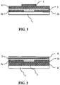
- FIG. 1 A top gate OFET in accordance with one preferred embodiment of the present invention is depicted schematically in FIG. 1
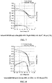
- a bottom gate OFET in accordance with another embodiment of the present invention is depicted schematically in FIG. 2 .
- FIG. 1 a schematic and simplified representation of a top gate OFET device in accordance with a preferred embodiment of the present invention is provided.
- Such OFET device includes a substrate (1), source and drain electrodes (2a, 2b), an OSC layer (3), a dielectric layer (4) encompassing a polycycloolefinic polymer as described above and below and serving as gate insulator, and a gate electrode (5).
- FIG. 2 a schematic and simplified representation of a bottom gate OFET device in accordance with another preferred embodiment of the present invention is provided.
- Such OFET device includes a substrate (1), a gate electrode (5), a dielectric layer (4) comprising a polycycloolefinic polymer as described above and below serving as gate insulator, source and drain electrodes (2a, 2b), an OSC layer (3), and optionally a passivation layer (6).
- the electrodes (2a, 2b, 5) are for example applied onto the substrate (1) or the dielectric layer (4) by a sputtering process, and can be patterned by etching and/or lithographic patterning.
- the OSC layer (3) and dielectric layer (4) can be applied by a coating or printing process as described above.
- the other components or functional layers of the OE and OFET devices can be selected from standard materials, and can be manufactured and applied to the device by standard methods. Suitable materials and manufacturing methods for these components and layers are known to a person skilled in the art and are described in the literature. Exemplary deposition methods include the liquid coating methods previously described as well as chemical vapor deposition (CVD) or physical vapor deposition methodologies.
- CVD chemical vapor deposition
- PVD physical vapor deposition
- the gate, source and drain electrodes in the OFET device embodiments in accordance with the present invention can be deposited or formed by liquid coating, such as spray-, dip-, web- or spin-coating, or by vacuum deposition methods including but not limited to physical vapor deposition (PVD), chemical vapor deposition (CVD) or thermal evaporation methods.
- Suitable electrode materials and deposition methods are known to the person skilled in the art. Suitable electrode materials include, without limitation, inorganic or organic materials, or composites of the two.
- Exemplary electrode materials include polyaniline, polypyrrole, poly(3,4-ethylenedioxy-thiophene) (PEDOT) or doped conjugated polymers, further dispersions or pastes of graphite or particles of metal such as Au, Ag, Cu, Al, Ni or their mixtures as well as sputter coated or evaporated metals such as Cu, Cr, Pt/Pd, Ag, Au or metal oxides such as indium tin oxide (ITO) F-doped ITO or Al-doped ZnO.
- Organometallic precursors can also be used and deposited from a liquid phase.
- the thickness of a functional layer for example a gate dielectric or OSC layer, in some preferred OE and OFET device embodiments in accordance with the present invention is from 0.001 (in case of a monolayer) to 10 ⁇ m. In some other preferred embodiments such thickness ranges from 0.001 to 1 ⁇ m, and in still other preferred embodiments from 5 nm to 500 nm, although other thicknesses or ranges of thickness are contemplated and thus are within the scope of the present invention.
- Suitable and preferred polymeric materials include, but are not limited to, alkyd resins, allyl esters, benzocyclobutenes, butadiene-styrene, cellulose, cellulose acetate, epoxide, epoxy polymers, ethylene-chlorotrifluoro ethylene copolymers, ethylene-tetra-fluoroethylene copolymers, fiber glass enhanced plastic, fluorocarbon polymers, hexafluoropropylene-vinylidene-fluoride copolymer, high density polyethylene, parylene, polyamide, polyimide, polyaramid, polydimethylsiloxane, polyethersulfone, poly-ethylene, polyethylenenaphthalate, polyethyleneterephthalate, polyketone, polymethylmethacrylate, polypropylene, polystyrene, polysulfone,
- the substrate can be any suitable material, for example, plastic, metal or glass material coated with one or more of the above listed materials. It will be understood that in forming such a substrate, methods, such as, extruding, stretching, rubbing or photochemical techniques can be employed to provide a homogeneous surface for device fabrication as well as to provide pre-alignment of an organic semiconductor material in order to enhance carrier mobility therein.
- pHexylNB poly(5-hexyl-bicyclo[2.2.1]hept-2-ene)
- pDecylNB poly(5-decyl-bicyclo[2.2.1]hept-2-ene)
- pBuDMMINB poly(1-(4-(bicyclo[2.2.1]hept-5-en-2-yl)butyl)-3,4-dimethyl-1H-pyrrole-2,5-dione)
- Zeonex480 ROMP polymerized norbornene from Nippon Zeon Co., Ltd.
- Topas 6013S-04 copolymer of norbornene and ethylene from Topas Advanced Polymers
- phr parts per hundred parts resin or polymer as described herein
- CPTX 1-chloro-4-propoxythioxanthone.
- pHexylNB and pDecylNB are according to formula (IA) of claim 1
- Zeonex480 is according to formula (III) of claim 1
- Topas6013S-04 is according to formula (II) of claim 1. Therefore, the only sample from Table 1 forming part of the claimed invention is the Zeonex480 sample.
- the polymer solutions formulated with BDA were spincoated on glass, dried for 4 minutes at 70°C and exposed to the UV light. Further, immersion into the carrier solvent for 30 seconds followed, then drying at 100°C. Film thicknesses were measured on Bruker Dektak before and after immersion into the solvent. Table 1 demonstrates the film thickness (FT) losses in percentage for each polymer.
- FT film thickness
- the dielectric constants were measured prior to the TFT device fabrication in order to enable calculation of charge carrier mobilities in these TFTs.
- the constants were extracted from the measured capacitance of individual dielectrics in a built capacitor device.
- the capacitor device was made by spincoating and curing the dielectric on ITO-coated glass, followed by deposition of the second electrode, in this case silver. Capacitor performance was then measured. Table 2.
- pHexylNB is according to formula (IA) of claim 1
- Zeonex480 is according to formula (III) of claim 1
- Topas6013S-04 is according to formula (II) of claim 1. Therefore, the only samples from Table 2 forming part of the claimed invention are the Zeonex480 samples.
- the dielectric constant measurements are summarized in Table 2. It is evident that inclusion of the cross-linker moiety, BDA, into the polymer results in a slight increase of the dielectric constant.
- TG top gate
- a series of solutions were formulated as summarized in Table 3 and then spin coated onto the OSC layer at given spin speeds.
- the reference OTFTs were fabricated without addition of bis-diazirine, BDA, to the pHexylNB formulation.
- the pristine film was baked at 100°C for 2 minutes and the films with added bis-diazirine, BDA, were annealed for 4 minutes at 70°C after deposition.
- pHexylNB is according to formula (IA) of claim 1, however the formulations from Table 3 are not forming part of the claimed invention.
- Table 3 Formulation Spin Conditions Curing Conditions Film Thickness (nm) pHexylNB, 12.5% in decane (Ref) 10s 500rpm, 30s 1800rpm No UV 800 pHexylNB, 12.5% in decane + 10phr BDA 10s 500rpm, 30s 1800rpm 1.95 J/cm 2 800 pHexylNB, 12.5% in decane + 30phr BDA 10s 500rpm, 30s 1800rpm 1.95 J/cm 2 800
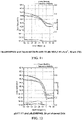
- FIGs. 3, 4 , and 5 demonstrate the performance on the above mentioned TG OTFTs. It can be clearly noticed that the device performance deteriorated with the cross-linking reaction induced by bis-diazirine (and possibly, by the UV-damage to the OSC material). However, it should be noted that devices still exhibit well-defined transistor performance.
- FIG. 3 shows a device incorporating pHexylNB dielectric without any bis-diazirine cross-linker added to the formulation or UV-dose applied to the film. This is therefore used as a reference and to illustrate changes in performance which occur through cross-linker in this experiment.
- FIGs. 4 and 5 show device performance obtained with dielectrics that were formulated with 10 and 30 phr of bis-diazirine, respectively, and UV cross-linked at 365nm. Comparing to the reference device in FIG. 3 , the notable performance degradation trend is observed with the increased loading of the cross-linker (e.g., decrease in mobility, increase in off-currents and hysteresis).
- pDecylNB is according to formula (IA) of claim 1, however the formulations from Table 4 are not forming part of the claimed invention.
- FIGs. 6 and 7 demonstrate the performance on the above mentioned TG OTFTs.
- FIG. 6 shows a device incorporating pDecylNB dielectric without any bis-diazirine cross-linker added to the formulation or UV-dose applied to the film. This is therefore used as a reference and to illustrate changes in performance which occur through cross-linker in this experiment.
- FIG. 7 shows device performance obtained with dielectric that was formulated with 10 phr of bis-diazirine and UV cross-linked at 365nm. Comparing to the reference device in FIG. 6 , some performance degradation was observed with the addition of the cross-linker (e.g., decrease in mobility, increase in off-current and hysteresis).
- the first formulation in Table 5 does not comprise the compound of formula (V) of claim1 and therefore does not form part of the claimed invention.
- FIGs. 8 and 9 demonstrate the performance on the above mentioned TG OTFTs.
- FIG. 8 shows a device incorporating Zeonex 480 dielectric without any bis-diazirine cross-linker added to the formulation or UV-dose applied to the film. This is therefore used as a reference and to illustrate changes in performance which occur through cross-linker in this experiment.
- FIG. 9 shows device performance obtained with dielectric that was formulated with 10 phr of bis-diazirine and UV cross-linked at 365 nm. Comparing to the reference device in FIG. 8 , the notable performance degradation is observed with the addition of the cross-linker (e.g., decrease in mobility, increase in off-current and hysteresis).
- Topas6013S-04 is according to formula (II) of claim 1, however the formulations from Table 6 do not form part of the claimed invention.
- FIGs. 10 and 11 demonstrate the performance on the above mentioned TG OTFTs.
- FIG. 10 shows a device incorporating Topas 6014S-04 dielectric without any bis-diazirine cross-linker added to the formulation or UV-dose applied to the film. This is therefore used as a reference and to illustrate changes in performance which occur through cross-linker in this experiment.
- FIG. 11 shows device performance obtained with dielectric that was formulated with 10 phr of bis-diazirine and UV cross-linked at 365 nm. Comparing to the reference device in FIG. 10 , some performance degradation was observed with the addition of the cross-linker (e.g., decrease in mobility, increase in off-current and hysteresis).
- standard bottom gate bottom contact devices ( FIG. 2 ) were constructed, using the OSC polymers lisicon ® SP500 and a p (di-indenothienothiophene)- co -(thienothiophene) (pDITT-TT).
- BG device fabrication with pHexylNB dielectric two dielectric formulations were prepared, as summarized in Table 7 and then spin coated onto the polymer OSC layer at given spin speeds. Two polymer OSC materials were used in this experiment.
- the reference OTFTs for each OSC polymer were fabricated with the standard BG dielectric pBuDMMINB that does not contain bis-diazirine in its formulation.
- the pBuDMMINB film was baked at 100°C for 2 minutes and the pHexylNB films with added bis-diazirine were annealed for 4 minutes at 70°C after deposition.
- FIGs. 12 , 13 , 14 and 15 demonstrate the performance on the above mentioned BG OTFTs.
- FIG. 12 shows a BG device incorporating pDITT-TT as OSC and pBuDMMINB as dielectric without any bis-diazirine cross-linker added to the formulation. This is therefore used as a reference and allows to track changes in performance with a different dielectric.
- FIG. 13 shows a BG device performance obtained with pDITT-TT as OSC and pHexylNB as dielectric that was formulated with 10 phr of bis-diazirine and UV cross-linked at 365nm. Comparing to the reference device in FIG. 12 , some performance degradation was observed with the new dielectric and change in crosslinking concept, decrease in mobility, increase in off-current and hysteresis.
- FIG. 14 shows a BG device incorporating lisicon ® SP500 polymer as OSC and pBuDMMINB as dielectric without any bis-diazirine cross-linker added to the formulation. This is therefore used as a reference and allows to track changes in performance with a different dielectric.
- FIG. 15 shows a BG device performance obtained with lisicon ® SP500 as OSC and pHexylNB as dielectric that was formulated with 10 phr of bis-diazirine and UV cross-linked at 365nm. Comparing to the reference device in FIG. 14 , some improved charge carrier mobility is observed. However, other device performance characteristics, such as off-currents and hysteresis, demonstrate some degradation with the change of dielectric and cross-linking concept.
Landscapes
- Chemical & Material Sciences (AREA)
- Engineering & Computer Science (AREA)
- Materials Engineering (AREA)
- Physics & Mathematics (AREA)
- Spectroscopy & Molecular Physics (AREA)
- Health & Medical Sciences (AREA)
- Chemical Kinetics & Catalysis (AREA)
- Medicinal Chemistry (AREA)
- Polymers & Plastics (AREA)
- Organic Chemistry (AREA)
- Thin Film Transistor (AREA)
- Addition Polymer Or Copolymer, Post-Treatments, Or Chemical Modifications (AREA)
Description
- The present invention relates to organic electronic compositions and devices thereof, specifically to organic dielectric compositions, and organic field effect transistors, comprising a dielectric layer that comprises a polycycloolefinic polymer and a diazirine compound.
- In recent years there has been growing interest in organic electronic (OE) devices, for example organic field effect transistors (OFET) for use in backplanes of display devices or logic capable circuits, and organic photovoltaic (OPV) devices. A conventional OFET has a gate electrode, a gate insulator layer made of a dielectric material (also referred to as "dielectric" or "gate dielectric"), source and drain electrodes, a semiconducting layer made of an organic semiconductor (OSC) material, and typically a passivation layer on top of the aforementioned layers to provide protection against environmental influence or against damage from subsequent device manufacturing steps.
- For many top gate (TG) OFET applications fluorodielectrics like Cytop® or Hyflon® polymers are usually deposited from fluorosolvents, to provide a dielectric layer with inherent low permittivity ("low-k") and good orthogonality to a number of OSC material classes. However, the use of such dielectrics has a number of drawbacks, with the main issue being lack of cross-linking functionality which is difficult to incorporate without modifying the permittivity. In addition, the use of fluorinated solvents is not preferred for environmental and cost reasons.
- It is desirable and advantageous to incorporate a reactive functionality into a dielectric which enables photo-patterning, as not only does this provide orthogonality to solvents employed in subsequent processing steps, but also allows for stack integration by the formation of via interconnects to the source and drain electrodes (S/D) below the dielectric and OSC layers, using photolithographic processes.
- In developing a crosslinkable top gate dielectric, the bulk properties of the material used, such as low k and solubility must be retained. It is also important to consider the functional group employed in the cross-linking reaction to ensure quantities of polar or charged by-product species are not generated as side products. Such species will become incorporated into the cross-linked dielectric, causing unwanted effects such as an increase in the k value, or the introduction of charged species may dope the OSC layer resulting in decreased performance and stability.
-
WO 2015/135622 A1 discloses an organic thin film transistor having its dielectric layer made of a polycycloolefinic polymer and a crosslinker. - Thus there is a need for solution processable dielectrics for the preparation of dielectric layers in OE devices, which have low permittivity, show good orthogonality to a number of OSC material classes, can be deposited from non-halogenated solvents, can be cross-linked to enable photo-patterning and stack integration by the formation of via interconnects to the S/D electrodes, and wherein the cross-linking reaction does not generate undesired polar or charged by-product species as side products.
- In particular, it is desired to have a UV crosslinkable dielectric with a solubility profile orthogonal to the OSC polymer, a permittivity as low as possible to give the highest TFT performance, and a cross-linking functional group, and/or cross-linking agents, incorporated to allow via interconnect patterning. The dielectric should, in conjunction with the OSC polymer, give high mobility, high on currents, and low off currents.
- The present invention enables satisfying the above needs by using a composition that encompasses a polycycloolefinic polymer in the dielectric layer of an OE device which does not contain a polar unit, is chemically inert, has an inherently low k, may have a pendant group or amorphous characteristics that imparts solubility and cross-linking functionality, and a cross-linking agent having a diazirine moiety.
- The present invention relates to an OE device comprising a dielectric layer, said dielectric layer comprising a polycycloolefinic polymer selected from the group consisting of:
- a) a random co-polymer having repeat units of formula (IA) and another olefin, said other olefin having the formula (II), where the repeat unit of formula (IA) is derived from a monomer of formula (I):


- b) a polymer of formula (III):

- c) a polymer of formula (IV):

- m is an
integer - each occurrence of R1, R2, R3 or R4 may be same or different and each independently is hydrogen or a hydrocarbyl selected from the group consisting of linear or branched (C1-C12)alkyl, (C3-C12)cycloalkyl, (C3-C12)cycloalkyl(C1-C12)alkyl, (C6-C12)bicycloalkyl, (C6-C12)bicycloalkyl(C1-C12)alkyl, (C7-C14)tricycloalkyl, (C7-C14)tricycloalkyl(C1-C12)alkyl, (C6-C10)aryl and (C6-C10)aryl(C1-C6)alkyl; and
- a diazirine compound of formula (V):

- wherein,
- L is a divalent linking or a spacer group selected from:
- -C(O)O-R7-OC(O)-, -C(O)O-R7-, -R7-OC(O)-R7-, -C(O)-R7-OC(O)-, -C(O)-R7-, -R7-C(O)-R7-, -O-R7-OC(O)-, -O-R7-O-, -O-R7-, -R7-O-R7-, -C(O)NH-(CH2)b-NH(CO)-, where b is 1 to 15, -C(O)NH-(CH2CH2O)c(CH2)d-NR5(CO)-, where c is 2 to 6 and d is 1 to 6, and each occurrence of R7 may be the same or different which is a divalent group independently selected from (C1-C12)alkyl, (C3-C12)cycloalkyl, (C6-C12)aryl, (C6-C12)aryl(C1-C12)alkyl, (C6-C10)heteroaryl, (C6-C10)heteroaryl(C1-C12)alkyl, -(CH2-CH2-O)a-, where a is an integer from 1 to 10;
- R5 and R6 are the same or different and each is independently selected from (C1-C12)alkyl, where portions of hydrogen on alkyl are replaced with fluorine, (C1-C12)perfluoroalkyl, (C6-C12)aryl, (C6-C12)aryl(C1-C12)alkyl, where portions of hydrogen on alkyl are replaced with fluorine, and (C6-C12)arylperfluoro(C1-C12)alkyl; and Ar1, Ar2 and Ar3 are the same or different and each is independently selected from (C6-C12)arylene or (C6-C12)heteroarylene group optionally substituted with a group selected from halogen, -OH, (C1-C4)alkyl, (C1-C4)alkoxy, (C6-C10)aryl, (C6-C12)aryloxy, (C6-C12)aryl(C1-C4)alkyl and (C6-C12)aryl(C1-C4)alkyloxy.
- m is an
- The disclosure further relates to a dielectric layer in an OE device, said dielectric layer comprising, or being obtained through the use of, a polycycloolefinic polymer of formulae (I), (II), (III) or (IV) as described above in combination with a diazirine compound of formula (V) as described above.
- Some embodiments in accordance with the present invention encompass a process of preparing a dielectric layer in an OE device through the use of a polycycloolefinic polymer of formulae (I), (II), (III) or (IV) as described herein.
- The aforementioned OE devices are, for example, Organic Field Effect Transistors (OFET), including Organic Thin Film Transistors (OTFT), Organic Light Emitting Diodes (OLED), Organic Photodetectors (OPD) or Organic Photovoltaic (OPV) devices. With regard to OFETs, such devices are inclusive of both top gate and bottom gate OFETs.
- Embodiments of the present invention are also inclusive of products or assemblies encompassing an OE device as described above and below. Such products or assemblies being Integrated Circuits (IC), Radio Frequency Identification (RFID) tags, security markings or security devices containing an RFID tag, Flat Panel Displays (FPD), backplanes of FPDs, backlights of FPDs, electrophotographic devices, electrophotographic recording devices, organic memory devices, pressure sensors, optical sensors, chemical sensors, biosensors or biochips.
- Embodiments of the invention are described below with reference to the following drawings.
-
FIG. 1 is a schematic representation of a top gate OFET device embodiment in accordance with the present invention; -
FIG. 2 is a schematic representation of a bottom gate OFET device embodiment in accordance with the present invention; -
FIGs. 3 to 6 are transfer curves of top gate OFET devices of Example 2. -
FIGs. 7 to 10 are transfer curves of top gate OFET devices of Example 3. - As used herein, the term Organic Field Effect Transistors (OFET) will be understood to be inclusive of the subclass of such devices known as Organic Thin Film Transistors (OTFTs).
- In addition, it will be understood that the terms "dielectric" and "insulating" are used interchangeably herein. Thus reference to an insulating material or layer is inclusive of a dielectric material or layer. Further, as used herein, the term "organic electronic device" will be understood to be inclusive of the term "organic semiconductor device" and the several specific implementations of such devices, such as the OFETs, are as defined above.
- As used herein, the terms "orthogonal" and "orthogonality" will be understood to mean chemical orthogonality. For example, an orthogonal solvent means a solvent which, when used in the deposition of a layer of a material dissolved therein on a previously deposited layer, does not dissolve said previously deposited layer.
- As used herein, the term "polymer" will be understood to mean a molecule that encompasses a backbone of one or more distinct types of repeating units (the smallest constitutional unit of the molecule) and is inclusive of the commonly known terms "oligomer", "copolymer", "homopolymer" and the like. Further, it will be understood that the term polymer is inclusive of, in addition to the polymer itself, small amounts of residues from initiators, catalysts and other elements attendant to the synthesis of such a polymer, where such residues are understood as not being covalently incorporated thereto. Further, while such residues, and other elements, are generally removed during post polymerization purification processes, trace amounts of such materials can be found to be mixed or co-mingled with the polymer such that they generally remain with the polymer when it is transferred between vessels or between solvents or dispersion media.
- As used herein, the term "small molecule" will be understood to mean a monomeric compound which typically does not carry a reactive group by which it can be reacted to form a polymer, and which is designated to be used in monomeric form. In contrast thereto, the term "monomer", unless stated otherwise, will be understood to mean a monomeric compound that carries one or more reactive functional groups by which it can be reacted to form an oligomer or a polymer.
- As used herein, the term "organic semiconductor (OSC) composition", also shortly referred to as "composition", means at least one organic semiconductor (OSC) compound and one or more other materials added to the at least one OSC compound to provide, or to modify, specific properties of the OSC composition and/or of the at least one OSC compound therein. It will be understood that an OSC composition is also a vehicle for carrying the OSC to a substrate to enable the forming of layers or structures thereon. Exemplary materials include, but are not limited to, solvents, volatile surfactants and adhesion promoters.
- As defined herein, the terms "polycycloolefin", "polycyclic olefin", and "norbornene-type" are used interchangeably and refer either to addition polymers or ring opening metathesis (ROMP) polymers, monomers or the resulting repeating unit, encompassing at least one norbornene moiety such as shown by either Structure (A1), (A2), (A3) or (A4) below. The simplest norbornene-type or polycyclic olefin monomer bicyclo[2.2.1]hept-2-ene (A1) is commonly referred to as norbornene. When norbornene is polymerized under addition polymerization conditions, the resulting repeat unit is of Structure (A1). When norbornene is polymerized under ROMP conditions, the resulting repeat unit is of Structure (A3), which is hydrogenated to Structure (A4).

- However, the term "norbornene-type repeating unit" or "norbornene-type monomer", as used herein, is understood to not only mean norbornene itself but also to refer to any substituted norbornene, or substituted and unsubstituted higher cyclic derivatives thereof, for example of Structures (B1), (B2), (B3) or (B4) respectively shown below, wherein m is an integer of zero or greater, as defined herein, where m = zero being the norbornene monomer of formula A1 or its respective repeat unit of formula A2 (for example addition polymer) or A3 or A4 (for example ROMP polymer).

- As will be discussed hereinafter, the use of a substituted norbornene-type monomer to form polymer embodiments of the present invention allows for the properties of such embodiments to be tailored to fulfill the needs of individual applications. The procedures and methods that have been developed to polymerize norbornene-type monomers having a variety of functional substituents, such as those described below, exhibit an outstanding flexibility and tolerance to various moieties and groups of the monomers. In addition to polymerization of monomers with a specific pendant group, monomers having a variety of distinct functionalities can be randomly polymerized to form a final material where the types and ratios of monomers used dictate the overall bulk properties of the resulting polymer.
- Some preferred embodiments of the present invention encompass an OE device comprising a dielectric layer, said dielectric layer comprising a polycycloolefinic polymer as given in claim 1 and a compound of formula (V) of claim 1.
- Accordingly, in some embodiments the present invention encompass an OE device comprising a dielectric layer, said dielectric layer comprising a random co-polymer comprising one or more distinct repeat units derived from a norbornene type monomer of formula (I), which are formed by addition polymerization techniques, and another olefin having the formula (II).
- Such addition polycyclic olefin polymers are well known in the literature, see for example, International Patent Publication No.
WO2015/135622 A1 . - Such cyclic olefin copolymers derived from norbornene are commercially available under the tradename Topas® and are represented herein above as polymers of formula (II), see generally
U. S. Patent No. 6,214,951 B1 . - In yet some other embodiments the present invention encompass an OE device comprising a dielectric layer, said dielectric layer comprising a polycycloolefinic polymer comprising one or more repeat units derived from a norbornene type monomer, which is polymerized under the conditions of ring opening metathesis polymerization (ROMP) and subsequently hydrogenated to obtain a polymer of formula (III) as described herein. Such cyclic olefin copolymers derived from norbornene are commercially available under the tradename Zeonex®, see generally
U. S. Patent No. 7,037,993 B2 . - In yet some other embodiments the present invention encompass an OE device comprising a dielectric layer, said dielectric layer comprising a polycycloolefinic polymer comprising one or more repeat units derived from a monomer, such as for example dicyclopentadiene, which is polymerized under the conditions of ring opening metathesis polymerization (ROMP) and subsequently hydrogenated to obtain a polymer of formula (IV) as described herein. Such cyclic olefin copolymers derived from norbornene are commercially available under the tradename Zeonor®, see generally
U. S. Patent No. 6,310,160 B1 . - Further preferred embodiments of the present invention encompass any one of the polycycloolefinic polymer according to claim 1 that is used for preparing a dielectric layer in an OE device. Any of the active groups in this polymeric chain, including the pendant groups, such as for example, alkyl or olefinic group can be cross-linked in a cross-linking reaction by a bis-diazirine cross-linker of formula (V) that initiates the reaction.
- In some preferred embodiments of the present invention the polycycloolefinic polymer is soluble in non-fluorinated solvents, preferably in inert solvents, and is deposited from a solution in an inert, non-fluorinated solvent or solvent composition. The solvent or solvent composition provides good orthogonality to an underlying OSC layer and renders the polycycloolefinic polymer especially suitable for use as dielectric layer in a top gate OFET device.
- The polycycloolefinic polymer, which is used in the dielectric layer, is according to claim 1.
- Examples of polycycloolefinic polymers are norbomene-type polymers. Examples of norbomene-type polymers encompass one or more norbornene-type polymers having one or more distinct types of repeating units of Formula IB

- The repeating units of Formula IB are formed from the corresponding norbornene-type monomers of Formula IC where Z, m and R1-4 are as defined above:

- Some preferred polymer embodiments in accordance with the present invention encompass repeating units of Formula IA derived from monomers of Formula I, where m is 0, 1 or 2. For other such embodiments m is 0 or 1, and for still other embodiments m is 0.
- Other preferred polymer embodiments of the present invention encompass repeating units of Formula IA derived from monomers of Formula I where only one of R1-4, for example R1, is different from H, and the others of R1-4 are H and m is 0.
- In yet some other preferred polymer embodiments of the present invention encompass polymers of Formula II where only one of R1-4, for example R1, is different from H, and the others of R1-4 are H and m is 0.
- In yet some other preferred polymer embodiments of the present invention encompass polymers of Formula III where only one of R1-4, for example R1, is different from H, and the others of R1-4 are H.
- In yet some other preferred polymer embodiments of the present invention encompass polymers of Formula IV where only one of R1-4, for example R1, is different from H, and the others of R1-4 are H.
- In some other embodiments of this invention any of the diazirine compound of formula (V) can be used as a cross-linking agent. Exemplary diazirines within the scope of the invention may be enumerated as follows:
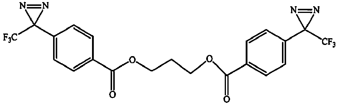


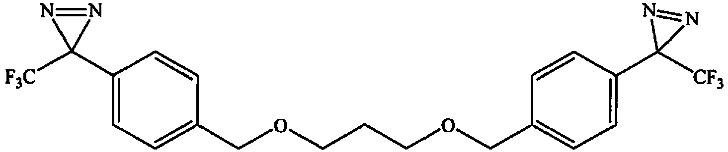


- N,N'-methylenebis(N -methyl-4-(3-(trifluoromethyl)-3H-diazirin-3-yl)benzamide).
- Other preferred embodiments in accordance with the present invention relate to a composition encompassing the polycycloolefinic polymer according to claim 1 and a compound of formula (V). The composition may also comprise a casting or printing solvent as already described hereinabove and hereinbelow.
- In some preferred composition embodiments in accordance with the present invention the solvent is selected from organic solvents as described hereinbelow and hereinabove. In other embodiments the solvent includes, without limitation, cyclohexylbenzene, mesitylene, indan, xylene, tetralin, diethylbenzene, cyclopentanone, benzyl acetate or combinations of the aforementioned.
- In other preferred composition embodiments in accordance with the present invention the concentration of the polycycloolefinic polymer in the composition is from 0.1% to 20%, preferably from 0.5% to 10%, and very preferably from 1% to 5%.
- The aforementioned concentration values refer to the composition encompassing the solvent(s) and all solid components such as the polycycloolefinic polymer which are dissolved in the solvent.
- In some preferred composition embodiments in accordance with the present disclosure the OSC can be an n- or p- type OSC. Effective OSCs exhibit a FET mobility of greater than 1×10⁻⁵ cm2V-1s-1.
- The OSC material employed for device embodiments in accordance with the present disclosure can be any conjugated molecule, for example, an aromatic molecule containing two or more, more specifically at least three aromatic rings. In some preferred OSC embodiments of the present invention, the OSC contains aromatic rings selected from 5-, 6- or 7-membered aromatic rings, while in other preferred embodiments the OSC contains aromatic rings selected from 5- or 6-membered aromatic rings. The OSC material can be a monomer, oligomer or polymer, including mixtures, dispersions and blends of one or more of monomers, oligomers or polymers.
- Each of the aromatic rings of the OSC optionally contains one or more hetero atoms selected from Se, Te, P, Si, B, As, N, O or S, generally from N, O or S. Further, the aromatic rings can be optionally substituted with fluoro, cyano, alkyl, alkoxy, polyalkoxy, thioalkyl, silyl, ethynylsilyl, optionally substituted secondary or tertiary alkylamine or arylamine, aryl or substituted aryl groups, wherein ethynylsilyl groups are represented by -C=C-SiR'R"R'", and substituted secondary or tertiary alkylamine or arylamine are represented by -N(R')(R"), wherein R' and R" are each independently H, optionally fluorinated C1-12 alkyl or optionally fluorinated C6-10 aryl.
- The aforementioned aromatic rings can be fused rings or linked with a conjugated linking group such as -C(T')=C(T")-, -C≡C-, -N(R"")-, -N=N-, (R"")=N-, -N=C(R"")-, where T' and T" each independently represent H, Cl, F, -C≡N or lower alkyl groups such as C1-4 alkyl groups and R"" is as defined above.
- In other preferred composition embodiments in accordance with the present disclosure,
- OSC materials that can be used include compounds, oligomers and derivatives of compounds selected from the group consisting of condensed aromatic hydrocarbons, such as, tetracene, chrysene, pentacene, pyrene, perylene, coronene, or soluble substituted and/or heterocylic derivatives of the aforementioned; oligomeric para substituted phenylenes such as p-quaterphenyl (p-4P), p-quinquephenyl (p-5P), p-sexiphenyl (p-6P) or soluble substituted derivatives of these; benzidine compounds; stilbene compounds; triazines; substituted metallo- or metal-free porphines, phthalocyanines, fluorophthalo-cyanines, naphthalocyanines or fluoronaphthalocyanines; C60 and C70 fullerenes; N,N'-dialkyl, substituted dialkyl, diaryl or substituted diaryl-1,4,5,8-naphthalene-tetracarboxylic diimide and fluoro derivatives; N,N'-dialkyl, substituted dialkyl, diaryl or substituted diaryl 3,4,9,10-perylenetetracarboxylic diimide; batho-phenanthroline; diphenoquinones; 1,3,4-oxadiazoles; 11,11,12,12-tetracyano-naptho-2,6-quinodimethane; α,α'-bis(dithieno[3,2-b2',3'-d]thiophene); 2,8-dialkyl, substituted dialkyl, diaryl or substituted diaryl anthradithiophene; 2,2'-bibenzo[1,2-b:4,5-b']dithiophene. Where a liquid deposition technique of the OSC is desired, compounds from the above list and derivatives thereof are limited to those that are soluble in an appropriate solvent or mixture of appropriate solvents.
- In other preferred composition embodiments in accordance with the present disclosure, the OSC materials are substituted oligoacenes such as pentacene, tetracene or anthracene, or heterocyclic derivatives thereof, more specifically oligoacenes that are substituted with alkylsilylethynyl groups, such as, bis(trialkylsilylethynyl) oligoacenes or bis(trialkylsilylethynyl) heteroacenes, for example, optionally fluorinated bis(trialkylsilylethynyl) anthradithiophenes, as disclosed for example in
US 6,690,029 ,WO 2005/055248 A1 orUS 7,385,221 . - Where appropriate and needed to adjust the rheological properties of the OSC composition, as described for example in
WO 2005/055248 A1 , some embodiments of the present disclosure employ OSC compositions that include one or more organic binders in addition to the polycycloolefinic polymer. In other embodiments the OSC composition does not include an organic binder in addition to the polycycloolefinic polymer. - Other preferred embodiments in accordance with the present disclosure relate to an OSC layer that is obtained through the use of an OSC composition in accordance with the present disclosure.
- Other preferred embodiments in accordance with the present disclosure relate to a process of preparing an OSC layer, encompassing depositing an OSC composition in accordance with the present disclosure onto a substrate and, in case the OSC composition encompasses a solvent, removing the solvent.
- In some preferred OSC layer embodiments in accordance with the present disclosure, deposition and/or forming of the OSC layer are performed using solution processing techniques. For example, a composition of the OSC and the polycycloolefinic polymer, typically a solution encompassing one or more organic solvents, can be deposited or formed using preferred techniques that include, but are not limited to, dip coating, slot-die coating spin coating, ink jet printing, letter-press printing, screen printing, doctor blade coating, roller printing, reverse-roller printing, offset lithography printing, flexographic printing, web printing, spray coating, brush coating, or pad printing, followed by the evaporation of the solvent employed to form such a solution. For example, an OSC material, a bank structure material and an organic dielectric material can each be deposited or formed by spin coating, flexographic printing, and inkjet printing techniques in an order appropriate to the device being formed.
- In other preferred OSC layer embodiments in accordance with the present disclosure the concentration of the polycycloolefinic polymer in the OSC layer after deposition and solvent removal is from 2.5 to 25%, more specifically from 10 to 15%.
- Other preferred embodiments in accordance with the present disclosure relate to an OE device encompassing an OSC layer and a passivation layer, wherein the OSC layer is obtained through the use of an OSC composition in accordance with the disclosure, and the passivation layer is obtained by vapor deposition of a p-xylylene, thus forming a layer of poly(p-xylylene).
- In some preferred OE device embodiments in accordance with the present disclosure the poly(p-xylylene) is Parylene C.
- Suitable process conditions for the vapor deposition process of p-xylylene are known to the skilled person and are described in the literature, for example, in P. Kramer et al., Journal of Polymer Science: Polymer Chemistry Edition, Vol. 22 (1984), pp. 475-491.
- In some preferred OE device embodiments in accordance with the present disclosure the OE device encompasses an OSC layer and a dielectric or passivation layer, wherein the OSC layer is obtained through the use of an OSC composition encompassing an OSC and a polycycloolefinic polymer having one or more reactive groups, and the dielectric or passivation layer is obtained by vapor deposition of a p-xylylene on the OSC layer, thus forming a layer of a poly(p-xylylene) on the OSC layer, and wherein the reactive groups of the polycycloolefinic polymer react with unsaturated groups of the p-xylylene at the interface between the OSC layer and the dielectric or passivation layer during vapor deposition of the p-xylylene, resulting in chemical bonding of the polycycloolefinic polymer of the OSC layer with the poly(p-xylylene) of the dielectric or passivation layer at the interface between the OSC layer and the dielectric or passivation layer.
- Preferred OE device embodiments in accordance with the present invention include, without limitation, organic field effect transistors (OFETs), organic thin film transistors (OTFTs), which can be top gate or bottom gate transistors, Organic Light Emitting Diodes (OLED), Organic Photodetecting (OPD) Devices or Organic Photovoltaic (OPV) Devices.
- Some preferred OE device embodiments in accordance with the present invention can be, for example, OFETs where the OSC is used as the active channel material, OPV devices where the OSC is used as charge carrier material, or organic rectifying diodes (ORDs) where the OSC is a layer element of such a diode. OSCs for such embodiments can be deposited by any of the previously discussed deposition methods, but as they are generally deposited or formed as blanket layers, solvent coated methods such as spray-, dip-, web- or spin-coating, or printing methods such as ink-jet printing, flexo printing or gravure printing, are typically employed to allow for ambient temperature processing.
- In some preferred OE device embodiments the OE device is a bottom gate or top gate OFET encompassing a gate dielectric layer encompassing a polycycloolefinic polymer as described above and below.
- In other preferred OE device embodiments the OE device is a bottom gate or top gate OFET encompassing a passivation layer encompassing a polycycloolefinic polymer as described above and below.
- Other preferred embodiments in accordance with the present invention relate to a process of preparing an OE device encompassing a dielectric or passivation layer comprising a polycycloolefinic polymer as described above and below, said OE device further encompassing an OSC layer being obtained by solution deposition of an OSC material.
- Other preferred embodiments of the present invention relate to a process of preparing an OE device, encompassing the following steps in an appropriate sequence:
- a) depositing an OSC material, preferably from an organic solution, to form an OSC layer,
- b) depositing source and drain electrodes,
- c) depositing a gate electrode,
- b) depositing a polycycloolefinic polymer and a compound of formula (V) as described above and below, preferably from an organic solution, to form a dielectric layer.
- A top gate OFET in accordance with one preferred embodiment of the present invention is depicted schematically in
FIG. 1 , and a bottom gate OFET in accordance with another embodiment of the present invention is depicted schematically inFIG. 2 . - Turning now to
FIG. 1 , a schematic and simplified representation of a top gate OFET device in accordance with a preferred embodiment of the present invention is provided. Such OFET device includes a substrate (1), source and drain electrodes (2a, 2b), an OSC layer (3), a dielectric layer (4) encompassing a polycycloolefinic polymer as described above and below and serving as gate insulator, and a gate electrode (5). - Other preferred embodiments in accordance with the present invention relate to a process for preparing a top gate OFET device, for example, as illustrated in
FIG. 1 , by a process encompassing: - a) forming source and drain electrodes (2a,2b) on a substrate (1),
- b) forming an OSC layer (3) by deposition of an OSC material, preferably from an organic solution, on the source and drain electrodes (2a,2b),
- c) forming a dielectric layer (4) by deposition of a polycycloolefinic polymer and a compound of formula (V) as described above and below, preferably from an organic solution, on the OSC layer (3),
- d) forming a gate electrode (5) on the dielectric layer (4).
- Turning now to
FIG. 2 , a schematic and simplified representation of a bottom gate OFET device in accordance with another preferred embodiment of the present invention is provided. Such OFET device includes a substrate (1), a gate electrode (5), a dielectric layer (4) comprising a polycycloolefinic polymer as described above and below serving as gate insulator, source and drain electrodes (2a, 2b), an OSC layer (3), and optionally a passivation layer (6). - Other preferred embodiments in accordance with the present invention relate to a process for preparing a bottom gate OFET device, for example, as illustrated in
FIG. 2 , by a process encompassing: - a) forming a gate electrode (5) on a substrate (1),
- b) forming a dielectric layer (4) by deposition of a polycycloolefinic polymer and a compound of formula (V) as described above and below, preferably from an organic solution, on the substrate (1) and the gate electrode (5),
- c) forming source and drain electrodes (2a, 2b) on the dielectric layer (4).
- d) forming an OSC layer (3) by deposition of an OSC material, preferably from an organic solution, on the source and drain electrodes (2a, 2b) and the dielectric layer (4),
- e) optionally forming a passivation layer (6) by deposition of a dielectric material on the OSC layer (3).
- In the aforementioned processes, the electrodes (2a, 2b, 5) are for example applied onto the substrate (1) or the dielectric layer (4) by a sputtering process, and can be patterned by etching and/or lithographic patterning. The OSC layer (3) and dielectric layer (4) can be applied by a coating or printing process as described above.
- The other components or functional layers of the OE and OFET devices, like the substrate and the gate, source and drain electrodes, can be selected from standard materials, and can be manufactured and applied to the device by standard methods. Suitable materials and manufacturing methods for these components and layers are known to a person skilled in the art and are described in the literature. Exemplary deposition methods include the liquid coating methods previously described as well as chemical vapor deposition (CVD) or physical vapor deposition methodologies.
- The gate, source and drain electrodes in the OFET device embodiments in accordance with the present invention can be deposited or formed by liquid coating, such as spray-, dip-, web- or spin-coating, or by vacuum deposition methods including but not limited to physical vapor deposition (PVD), chemical vapor deposition (CVD) or thermal evaporation methods. Suitable electrode materials and deposition methods are known to the person skilled in the art. Suitable electrode materials include, without limitation, inorganic or organic materials, or composites of the two. Exemplary electrode materials include polyaniline, polypyrrole, poly(3,4-ethylenedioxy-thiophene) (PEDOT) or doped conjugated polymers, further dispersions or pastes of graphite or particles of metal such as Au, Ag, Cu, Al, Ni or their mixtures as well as sputter coated or evaporated metals such as Cu, Cr, Pt/Pd, Ag, Au or metal oxides such as indium tin oxide (ITO) F-doped ITO or Al-doped ZnO. Organometallic precursors can also be used and deposited from a liquid phase.
- Generally, the thickness of a functional layer, for example a gate dielectric or OSC layer, in some preferred OE and OFET device embodiments in accordance with the present invention is from 0.001 (in case of a monolayer) to 10 µm. In some other preferred embodiments such thickness ranges from 0.001 to 1 µm, and in still other preferred embodiments from 5 nm to 500 nm, although other thicknesses or ranges of thickness are contemplated and thus are within the scope of the present invention.
- Various substrates may be used for the fabrication of the OE device embodiments of the present invention. For example, glass or polymeric materials are most often used. Suitable and preferred polymeric materials include, but are not limited to, alkyd resins, allyl esters, benzocyclobutenes, butadiene-styrene, cellulose, cellulose acetate, epoxide, epoxy polymers, ethylene-chlorotrifluoro ethylene copolymers, ethylene-tetra-fluoroethylene copolymers, fiber glass enhanced plastic, fluorocarbon polymers, hexafluoropropylene-vinylidene-fluoride copolymer, high density polyethylene, parylene, polyamide, polyimide, polyaramid, polydimethylsiloxane, polyethersulfone, poly-ethylene, polyethylenenaphthalate, polyethyleneterephthalate, polyketone, polymethylmethacrylate, polypropylene, polystyrene, polysulfone, polytetrafluoroethylene, polyurethanes, polyvinylchloride, polycycloolefin, silicone rubbers, and silicones, where polyethyleneterephthalate, polyimide, polycycloolefin and polyethylenenaphthalate materials have been found most appropriate. Additionally, for some preferred embodiments of the present invention the substrate can be any suitable material, for example, plastic, metal or glass material coated with one or more of the above listed materials. It will be understood that in forming such a substrate, methods, such as, extruding, stretching, rubbing or photochemical techniques can be employed to provide a homogeneous surface for device fabrication as well as to provide pre-alignment of an organic semiconductor material in order to enhance carrier mobility therein.
- Unless the context clearly indicates otherwise, as used herein plural forms of the terms herein are to be construed as including the singular form and vice versa.
- It will be appreciated that variations to the foregoing embodiments of the invention can be made while still falling within the scope of the invention.
- All of the features disclosed in this specification can be combined in any combination, except combinations where at least some of such features and/or steps are mutually exclusive. In particular, the features of the invention are applicable to all aspects of the invention and can be used in any combination. Likewise, features described in non-essential combinations can be used separately (not in combination).
- The invention will now be described in more detail by reference to the following examples, which are illustrative only and do not limit the scope of the invention.
- The following abbreviations have been used hereinbefore and hereafter in describing some of the compounds, instruments and/or methods employed to illustrate certain of the embodiments of this invention:
pHexylNB: poly(5-hexyl-bicyclo[2.2.1]hept-2-ene), pDecylNB: poly(5-decyl-bicyclo[2.2.1]hept-2-ene), pBuDMMINB: poly(1-(4-(bicyclo[2.2.1]hept-5-en-2-yl)butyl)-3,4-dimethyl-1H-pyrrole-2,5-dione), Zeonex480: ROMP polymerized norbornene from Nippon Zeon Co., Ltd., Topas 6013S-04: copolymer of norbornene and ethylene from Topas Advanced Polymers, phr: parts per hundred parts resin or polymer as described herein, CPTX: 1-chloro-4-propoxythioxanthone. - Above and below, unless stated otherwise percentages are per cent by weight and temperatures are given in degrees Celsius (°C). The values of the dielectric constant ε ("permittivity") refer to values taken at 20 °C and 1,000 Hz.
- The efficiency of crosslinking with bis-diazirine, propane-1,3-diyl bis(4-(3-(trifluoromethyl)-3H-diazirin-3-yl)benzoate) (BDA), using a light source at 365 nm and at a dosage as summarized in Table 1 was tested with four polymers: pHexylNB,
- pDecylNB, Zeonex480 and Topas 6013S-04. pHexylNB and pDecylNB are according to formula (IA) of claim 1, Zeonex480 is according to formula (III) of claim 1, while Topas6013S-04 is according to formula (II) of claim 1. Therefore, the only sample from Table 1 forming part of the claimed invention is the Zeonex480 sample.
Table 1 Sample FT loss (%) pHexylNB, 12.5% decane + 10 phr BDA, 1.95 J/ cm 24 pHexylNB, 12.5% decane + 10 phr BDA, 0.8 J/ cm 25 pHexylNB, 12.5% decane + 10 phr BDA, 5 min@140°C 17 pHexylNB, 12.5% decane + 30 phr BDA, 1.95J/ cm 22 pHexylNB, 12.5% decane + 30 phr BDA, 0.8J/ cm 22 pHexylNB, 12.5% decane + 30 phr BDA, 5min@140° C 3 pDecylNB, 12% in decane + 10 phr BDA, 1.95 J/ cm 27 pDecylNB, 12% in decane + 10 phr BDA, 0.78 J/ cm 26 pDecylNB, 12% in decane + 10 phr BDA, 5 mins@140° C 50 pDecylNB, 12% in decane + 10 phr BDA, 15 mins@140°C 47 Zeonex 480, 10% in p-menthane + 10 phr BDA, 1.95 J/cm223 Topas 6013S-04, 8% in p-menthane + 10 phr BDA, 1.95 J/ cm 26 FT - film thickness - The polymer solutions formulated with BDA were spincoated on glass, dried for 4 minutes at 70°C and exposed to the UV light. Further, immersion into the carrier solvent for 30 seconds followed, then drying at 100°C. Film thicknesses were measured on Bruker Dektak before and after immersion into the solvent. Table 1 demonstrates the film thickness (FT) losses in percentage for each polymer. For pHexylNB, crosslinking was investigated with the standard loading of the crosslinker (10 part per hundred of polymer) and a much higher loading. Thermal treatment efficiency has also been investigated.
- From the results summarized in Table 1, it is apparent that BDA functions as an excellent crosslinker at 365 nm on a range of polymers tested. However, BDA functions less efficiently under thermal treatment alone.
- To assess the OTFT performance of the materials they were used to construct standard top gate, bottom contact OFET devices, using the OSC polymer lisicon®SP400 (obtained from Merck GmbH).
- The dielectric constants (k-values) were measured prior to the TFT device fabrication in order to enable calculation of charge carrier mobilities in these TFTs. The constants were extracted from the measured capacitance of individual dielectrics in a built capacitor device. The capacitor device was made by spincoating and curing the dielectric on ITO-coated glass, followed by deposition of the second electrode, in this case silver. Capacitor performance was then measured.
Table 2. Sample Dielectric constant pHexylNB + 10 phr BDA, no UV-exposure 2.05 pHexylNB + 10 phr BDA, 1.95 J/cm2 2.09 Zeonex 480, 10% in p-menthane + 10 phr BDA, no UV-exposure 2.23 Zeonex 480, 10% in p-menthane + 10 phr BDA, 1.95 J/cm22.32 Topas 6013S-04, 8% in p-menthane + 10 phr BDA, no UV-exposure 2.20 Topas 6013S-04, 8% in p-menthane + 10 phr BDA, 1.95 J/cm2 2.36 - pHexylNB is according to formula (IA) of claim 1, Zeonex480 is according to formula (III) of claim 1, while Topas6013S-04 is according to formula (II) of claim 1. Therefore, the only samples from Table 2 forming part of the claimed invention are the Zeonex480 samples. The dielectric constant measurements are summarized in Table 2. It is evident that inclusion of the cross-linker moiety, BDA, into the polymer results in a slight increase of the dielectric constant.
- For the top gate (TG) device fabrication with pHexylNB as a dielectric layer, a series of solutions were formulated as summarized in Table 3 and then spin coated onto the OSC layer at given spin speeds. The reference OTFTs were fabricated without addition of bis-diazirine, BDA, to the pHexylNB formulation. The pristine film was baked at 100°C for 2 minutes and the films with added bis-diazirine, BDA, were annealed for 4 minutes at 70°C after deposition. pHexylNB is according to formula (IA) of claim 1, however the formulations from Table 3 are not forming part of the claimed invention.
Table 3 Formulation Spin Conditions Curing Conditions Film Thickness (nm) pHexylNB, 12.5% in decane (Ref) 10s 500rpm, 30s 1800rpm No UV 800 pHexylNB, 12.5% in decane + 10phr BDA 10s 500rpm, 30s 1800rpm 1.95 J/cm2 800 pHexylNB, 12.5% in decane + 30phr BDA 10s 500rpm, 30s 1800rpm 1.95 J/cm2 800 -
FIGs. 3, 4 , and5 demonstrate the performance on the above mentioned TG OTFTs. It can be clearly noticed that the device performance deteriorated with the cross-linking reaction induced by bis-diazirine (and possibly, by the UV-damage to the OSC material). However, it should be noted that devices still exhibit well-defined transistor performance. -
FIG. 3 shows a device incorporating pHexylNB dielectric without any bis-diazirine cross-linker added to the formulation or UV-dose applied to the film. This is therefore used as a reference and to illustrate changes in performance which occur through cross-linker in this experiment. -
FIGs. 4 and5 show device performance obtained with dielectrics that were formulated with 10 and 30 phr of bis-diazirine, respectively, and UV cross-linked at 365nm. Comparing to the reference device inFIG. 3 , the notable performance degradation trend is observed with the increased loading of the cross-linker (e.g., decrease in mobility, increase in off-currents and hysteresis). - For the TG device fabrication with pDecylNB dielectric, two solutions were formulated as summarized in Table 4 and then spin coated onto the OSC layer at given spin speeds. The reference OTFTs were fabricated without addition of bis-diazirine to the pDecylNB formulation. The pristine film was baked at 100°C for 2 minutes and the films with added bis-diazirine were annealed for 4 minutes at 70°C after deposition.
Table 4 Formulation Spin Conditions Curing Conditions Film Thickness (nm) pDecylNB, 12 % in decane (Ref) 30s 1100rpm No UV 760 pDecylNB, 12 % in decane + 10 phr BDA 30s 1100rpm 1.95 J/cm2 760 - pDecylNB is according to formula (IA) of claim 1, however the formulations from Table 4 are not forming part of the claimed invention.
-
FIGs. 6 and7 demonstrate the performance on the above mentioned TG OTFTs. -
FIG. 6 shows a device incorporating pDecylNB dielectric without any bis-diazirine cross-linker added to the formulation or UV-dose applied to the film. This is therefore used as a reference and to illustrate changes in performance which occur through cross-linker in this experiment. -
FIG. 7 shows device performance obtained with dielectric that was formulated with 10 phr of bis-diazirine and UV cross-linked at 365nm. Comparing to the reference device inFIG. 6 , some performance degradation was observed with the addition of the cross-linker (e.g., decrease in mobility, increase in off-current and hysteresis). - For the TG device fabrication with Zeonex 480 dielectric, two solutions were formulated as summarized in Table 5 and then spin coated onto the OSC layer at given spin speeds. The reference OTFTs were fabricated without addition of bis-diazirine to the Zeonex 480 formulation. The pristine film was baked at 100°C for 2 minutes and the films with added bis-diazirine were annealed for 4 minutes at 70°C after deposition.
Table 5 Formulation Spin Conditions Curing Conditions Film Thickness (nm) Zeonex 480, 10% in p-menthane30s 1400rpm No UV 800 Zeonex 480, 10% in p-menthane + 10 phr BDA30s 1400rpm 1.95 J/cm2 850 - The first formulation in Table 5 does not comprise the compound of formula (V) of claim1 and therefore does not form part of the claimed invention.
-
FIGs. 8 and9 demonstrate the performance on the above mentioned TG OTFTs. -
FIG. 8 shows a device incorporating Zeonex 480 dielectric without any bis-diazirine cross-linker added to the formulation or UV-dose applied to the film. This is therefore used as a reference and to illustrate changes in performance which occur through cross-linker in this experiment. -
FIG. 9 shows device performance obtained with dielectric that was formulated with 10 phr of bis-diazirine and UV cross-linked at 365 nm. Comparing to the reference device inFIG. 8 , the notable performance degradation is observed with the addition of the cross-linker (e.g., decrease in mobility, increase in off-current and hysteresis). - For the TG device fabrication with Topas 6013S-04 dielectric, two solutions were formulated as summarized in Table 6 and then spin coated onto the OSC layer at given spin speeds. The reference OTFTs were fabricated without addition of bis-diazirine to the Topas 6013S-04 formulation. The pristine film was baked at 100°C for 2 minutes and the films with added bis-diazirine were annealed for 4 minutes at 70°C after deposition.
Table 6 Formulation Spin Conditions Curing Conditions Film Thickness (nm) Topas 6013S-04, 8 % in p-menthane 30s 1200rpm No UV 690 Topas 6013S-04, 8 % in p-menthane + 10phr BDA 30s 1200rpm 1.95 J/cm2 680 - Topas6013S-04 is according to formula (II) of claim 1, however the formulations from Table 6 do not form part of the claimed invention.
-
FIGs. 10 and11 demonstrate the performance on the above mentioned TG OTFTs. -
FIG. 10 shows a device incorporating Topas 6014S-04 dielectric without any bis-diazirine cross-linker added to the formulation or UV-dose applied to the film. This is therefore used as a reference and to illustrate changes in performance which occur through cross-linker in this experiment. -
FIG. 11 shows device performance obtained with dielectric that was formulated with 10 phr of bis-diazirine and UV cross-linked at 365 nm. Comparing to the reference device inFIG. 10 , some performance degradation was observed with the addition of the cross-linker (e.g., decrease in mobility, increase in off-current and hysteresis). - To assess the OTFT performance of the materials further, standard bottom gate bottom contact devices (
FIG. 2 ) were constructed, using the OSC polymers lisicon®SP500 and a p(di-indenothienothiophene)-co-(thienothiophene) (pDITT-TT). - For the BG device fabrication with pHexylNB dielectric, two dielectric formulations were prepared, as summarized in Table 7 and then spin coated onto the polymer OSC layer at given spin speeds. Two polymer OSC materials were used in this experiment. The reference OTFTs for each OSC polymer were fabricated with the standard BG dielectric pBuDMMINB that does not contain bis-diazirine in its formulation. The pBuDMMINB film was baked at 100°C for 2 minutes and the pHexylNB films with added bis-diazirine were annealed for 4 minutes at 70°C after deposition.
Table 7 Formulation Spin conditions Curing conditions Film Thickness, nm pBuDMMINB with 1 phr CPTX, 17.5% in MAK 30s 2000rpm 2.60 J/cm2 1.27 mm pHexylNB, 12% in decane with 10 phr BDA 30s 1500rpm 1.95 J/cm2 0.992 -
FIGs. 12 ,13 ,14 and15 demonstrate the performance on the above mentioned BG OTFTs. -
FIG. 12 shows a BG device incorporating pDITT-TT as OSC and pBuDMMINB as dielectric without any bis-diazirine cross-linker added to the formulation. This is therefore used as a reference and allows to track changes in performance with a different dielectric. -
FIG. 13 shows a BG device performance obtained with pDITT-TT as OSC and pHexylNB as dielectric that was formulated with 10 phr of bis-diazirine and UV cross-linked at 365nm. Comparing to the reference device inFIG. 12 , some performance degradation was observed with the new dielectric and change in crosslinking concept, decrease in mobility, increase in off-current and hysteresis. -
FIG. 14 shows a BG device incorporating lisicon®SP500 polymer as OSC and pBuDMMINB as dielectric without any bis-diazirine cross-linker added to the formulation. This is therefore used as a reference and allows to track changes in performance with a different dielectric. -
FIG. 15 shows a BG device performance obtained with lisicon®SP500 as OSC and pHexylNB as dielectric that was formulated with 10 phr of bis-diazirine and UV cross-linked at 365nm. Comparing to the reference device inFIG. 14 , some improved charge carrier mobility is observed. However, other device performance characteristics, such as off-currents and hysteresis, demonstrate some degradation with the change of dielectric and cross-linking concept.
Claims (14)
- An organic electronic (OE) device comprising a dielectric layer (4), said dielectric layer comprising a polycycloolefinic polymer selected from the group consisting of:a) a random co-polymer having repeat units of formula (IA) and another olefin, said other olefin having the formula (II), where the repeat unit of formula (IA) is derived from a monomer of formula (I):

 b) a polymer of formula (III):
 c) a polymer of formula (IV):
 m is an integer 0, 1 or 2;each occurrence of R1, R2, R3 or R4 may be same or different and eachand a compound of formula (V):
independently is hydrogen or a hydrocarbyl selected from the group consisting of linear or branched (C1-C12)alkyl, (C3-C12)cycloalkyl, (C3-C12)cycloalkyl(C1-C12)alkyl, (C6-C12)bicycloalkyl, (C6-C12)bicycloalkyl(C1-C12)alkyl, (C7-C14)tricycloalkyl, (C7-C14)tricycloalkyl(C1-C12)alkyl, (C6-C10)aryl and (C6-C10)aryl(C1-C6)alkyl;
L is a divalent linking or a spacer group selected from:-C(O)O-R7-OC(O)-, -C(O)O-R7-, -R7-OC(O)-R7-, -C(O)-R7-OC(O)-, -C(O)-R7-,-R7-C(O)-R7-, -O-R7-OC(O)-, -O-R7-O-, -O-R7-, -R7-O-R7-, -C(O)NH-(CH2)b-NH( CO)-, where b is 1 to 15, -C(O)NH-(CH2CH2O)c(CH2)d-NR5(CO)-, where c is 2 to 6 and d is 1 to 6, and each occurrence of R7 may be the same or different which is a divalent group independently selected from (C1-C12)alkyl, (C3-C12)cycloalkyl, (C6-C12)aryl, (C6-C12)aryl(C1-C12)alkyl, (C6-C10)heteroaryl, (C6-C10)heteroaryl(C1-C12)alkyl, -(CH2-CH2-O)a-, where a is an integer from 1 to 10;R5 and R6 are the same or different and each is independently selected from (C1-C12)alkyl, where portions of hydrogen on alkyl are replaced with fluorine, (C1-C12)perfluoroalkyl, (C6-C12)aryl, (C6-C12)aryl(C1-C12)alkyl, where portions of hydrogen on alkyl are replaced with fluorine, and (C6-C12)arylperfluoro(C1-C12)alkyl; andAr1, Ar2 and Ar3 are the same or different and each is independently selected from (C6-C12)arylene or (C6-C12)heteroarylene group optionally substituted with a group selected from halogen, -OH, (C1-C4)alkyl, (C1-C4)alkoxy, (C6-C10)aryl, (C6-C12)aryloxy, (C6-C12)aryl(C1-C4)alkyl and (C6-C12)aryl(C1-C4)alkyloxy. - The OE device according to claim 1, wherein the polycycloolefinic polymer is a random co-polymer having repeat units of formula (IA) and another olefin of Formula (II);or wherein the polycycloolefinic polymer is of Formula (III);or wherein the polycycloolefinic polymer is of Formula (IV).
- The OE device according to one or more of claims 1 or 2, which comprises one or more compounds of formula (V) as a crosslinker agent.
- The OE device according to one or more of claims 1 to 3, wherein the cross-linker compound is selected from the group consisting of:


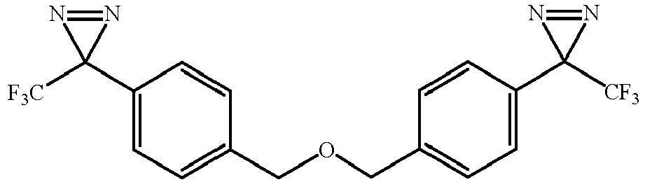


- The OE device according to one or more of claims 1 to 4, which is an Organic Field Effect Transistor (OFET), Organic Thin Film Transistor (OTFT), Organic Light Emitting Diode (OLED) or Organic Photovoltaic (OPV) device or Organic Photodetector (OPD).
- The OE device according to claim 5, which is a top gate OFET or bottom gate OFET.
- The top gate OFET according to claim 6, which comprises a substrate (1), source and drain electrodes (2a, 2b), an organic semiconductor (OSC) layer (3), a dielectric layer (4) comprising a polycycloolefinic polymer as defined in one or more of claims 1 to 4 and serving as gate insulator, and gate electrode (5).
- A process for preparing an OFET according to claim 7, which comprises:A) forming source and drain electrodes (2a, 2b) on a substrate (1),B) forming an OSC layer (3) by deposition of an OSC material on the source and drain electrodes (2a, 2b),C) forming a dielectric layer (4) by deposition of a polycycloolefinic polymer and a compound of formula (V) as defined in one or more of claims 1 to 10 on the OSC layer (3),D) forming a gate electrode (5) on the dielectric layer (4).
- The bottom gate OFET according to claim 6, which comprises a substrate (1), a gate electrode (5), a dielectric layer (4) comprising a polycycloolefinic polymer as defined in one or more of claims 1 to 10 and serving as gate insulator, source and drain electrodes (2a, 2b), an OSC layer (3), and optionally a passivation layer (6).
- A process for preparing an OFET according to claim 9, which comprises:A) forming a gate electrode (5) on a substrate (1),B) forming a dielectric layer (4) by deposition of a polycycloolefinic polymer and a compound of formula (V) as defined in one or more of claims 1 to 10 on the substrate (1) and the gate electrode (5),C) forming source and drain electrodes (2a, 2b) on the dielectric layer (4).D) forming an OSC layer (3) by deposition of an OSC material on the source and drain electrodes (2a, 2b) and the dielectric layer (4),E) optionally forming a passivation layer (6) on the OSC layer (3).
- A process according to claim 8 or 10, wherein the OSC material of the OSC layer (3) and the polycycloolefinic polymer of the dielectric layer (4) are deposited from an organic solution.
- A product or assembly comprising an OE device according to one or more of claims 1 to 9, which is an Integrated Circuit (IC), a Radio Frequency Identification (RFID) tag, a security marking or security device containing an RFID tag, a Flat Panel Display (FPD), a backplane of an FPD, a backlight of an FPD, an electrophotographic device, an electrophotographic recording device, an organic memory device, a pressure sensor, an optical sensor, a chemical sensor, a biosensor or a biochip.
- A composition comprising:a) a random co-polymer having repeat units of formula (IA) and another olefin having the formula (II), where the repeat unit of formula (IA) is derived from a monomer of formula (I):

 b) a polymer of formula (III): or
 c) a polymer of formula (IV):
 whereinm is an integer 0, 1 or 2;each occurrence of R1, R2, R3 or R4 may be same or different and each independently is hydrogen or a hydrocarbyl selected from the group consisting of linear or branched (C1-C12)alkyl, (C3-C12)cycloalkyl, (C3-C12)cycloalkyl(C1-C12)alkyl, (C6-C12)bicycloalkyl, (C6-C12)bicycloalkyl(C1-C12)alkyl, (C7-C14)tricycloalkyl, (C7-C14)tricycloalkyl(C1-C12)alkyl, (C6-C10)aryl and (C6-C10)aryl(C1-C6)alkyl; anda compound of formula (V):
 wherein,L is a divalent linking or a spacer group selected from:-C(O)O-R7-OC(O)-, -C(O)O-R7-, -R7-OC(O)-R7-, -C(O)-R7-OC(O)-, -C(O)-R7-,-R7-C(O)-R7-, -O-R7-OC(O)-, -O-R7-O-, -O-R7-, -R7-O-R7-, -C(O)NH-(CH2)b-NH( CO)-, where b is 1 to 15, -C(O)NH-(CH2CH2O),(CH2)d-NR5(CO)-, where c is 2 to 6 and d is 1 to 6, and each occurrence of R7 may be the same or different which is a divalent group independently selected from (C1-C12)alkyl, (C3-C12)cycloalkyl, (C6-C12)aryl, (C6-C12)aryl(C1-C12)alkyl, (C6-C10)heteroaryl, (C6-C10)heteroaryl(C1-C12)alkyl, -(CH2-CH2-O)a-, where a is an integer from 1 to 10;R5 and R6 are the same or different and each is independently selected from (C1-C12)alkyl, where portions of hydrogen on alkyl are replaced with fluorine, (C1-C12)perfluoroalkyl, (C6-C12)aryl, (C6-C12)aryl(C1-C12)alkyl, where portions of hydrogen on alkyl are replaced with fluorine, and (C6-C12)arylperfluoro(C1-C12)alkyl; andAr1, Ar2 and Ar3 are the same or different and each is independently selected from (C6-C12)arylene or (C6-C12)heteroarylene group optionally substituted with a group selected from halogen, -OH, (C1-C4)alkyl, (C1-C4)alkoxy, (C6-C10)aryl, (C6-C12)aryloxy, (C6-C12)aryl(C1-C4)alkyl and (C6-C12)aryl(C1-C4)alkyloxy.
 - The composition as defined in claim 13 wherein said compound of formula (V) is selected from the group consisting of:


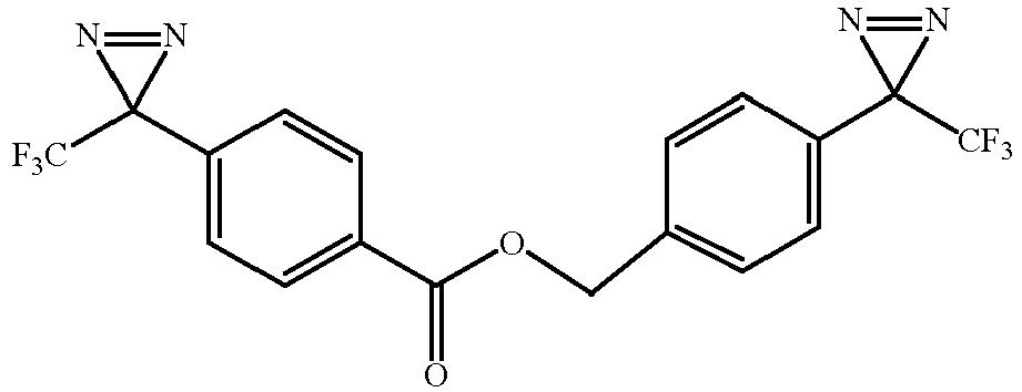
Applications Claiming Priority (2)
| Application Number | Priority Date | Filing Date | Title |
|---|---|---|---|
| US201662311598P | 2016-03-22 | 2016-03-22 | |
| PCT/US2017/023520 WO2017165478A1 (en) | 2016-03-22 | 2017-03-22 | Diazirine containing organic electronic compositions and device thereof |
Publications (2)
| Publication Number | Publication Date |
|---|---|
| EP3433884A1 EP3433884A1 (en) | 2019-01-30 |
| EP3433884B1 true EP3433884B1 (en) | 2023-01-11 |
Family
ID=58609962
Family Applications (1)
| Application Number | Title | Priority Date | Filing Date |
|---|---|---|---|
| EP17719042.8A Active EP3433884B1 (en) | 2016-03-22 | 2017-03-22 | Diazirine containing organic electronic compositions and device thereof |
Country Status (4)
| Country | Link |
|---|---|
| US (2) | US10256409B2 (en) |
| EP (1) | EP3433884B1 (en) |
| CN (1) | CN108886096B (en) |
| WO (1) | WO2017165478A1 (en) |
Families Citing this family (15)
| Publication number | Priority date | Publication date | Assignee | Title |
|---|---|---|---|---|
| US11142662B2 (en) * | 2018-12-21 | 2021-10-12 | Promerus, Llc | High impact strength 3D printing materials derived from polycycloolefin monomers and crosslinkers |
| CA3137379A1 (en) * | 2019-04-26 | 2020-10-29 | Xlynx Materials Inc. | Diazirine-based molecules and uses thereof |
| CN114450812A (en) * | 2019-06-24 | 2022-05-06 | 弗莱克英纳宝有限公司 | Modification of stress response and adhesion behavior of dielectrics by tuning mechanical properties |
| EP4093599B1 (en) | 2020-02-28 | 2023-11-29 | Carbon, Inc. | Methods of making a three-dimensional object |
| TWI878633B (en) * | 2020-10-30 | 2025-04-01 | 日商住友電木股份有限公司 | Polycyclic-olefinic compositions for low-loss films having improved thermal properties |
| TWI908911B (en) * | 2020-10-30 | 2025-12-21 | 日商住友電木股份有限公司 | Shelf life stable and improved mass polymerizable polycyclic-olefinic compositions |
| CN114790171A (en) * | 2021-01-26 | 2022-07-26 | 中国科学院化学研究所 | A kind of diaziridine crosslinking agent and preparation method and application thereof |
| JP2024509573A (en) * | 2021-03-09 | 2024-03-04 | エクスリンクス マテリアルズ インク | Aryl ether diazirines used for crosslinking and adhesion of polymers |
| US20220298399A1 (en) * | 2021-03-19 | 2022-09-22 | Facebook Technologies, Llc | Synthesis and use of multi-functional diazirine adhesives for elastomer bonding |
| DE102021125407A1 (en) * | 2021-09-30 | 2023-03-30 | Polymer Competence Center Leoben Gmbh | Method of making a dielectric for a capacitor and Method of making a capacitor and capacitor |
| WO2023205071A2 (en) * | 2022-04-18 | 2023-10-26 | Colorado State University Research Foundation | Dynamically crosslinked multiblock copolymers for compatibilizing immiscible mixed plastics |
| CN115312971A (en) * | 2022-08-18 | 2022-11-08 | 江阴纳力新材料科技有限公司 | Polymer film, preparation method thereof and composite current collector |
| WO2024113041A1 (en) * | 2022-12-02 | 2024-06-06 | Xlynx Materials Inc. | Selectively activated diazirine-containing molecules and polymers |
| KR102895011B1 (en) * | 2023-12-08 | 2025-12-02 | 포항공과대학교 산학협력단 | Photocrosslinking agent containing bisdiazirine, photocatalytic reforming and hydrogen production device using the same |
| CN117924964A (en) * | 2023-12-22 | 2024-04-26 | 山东中康国创先进印染技术研究院有限公司 | Carbene dye containing diazepine structure and preparation method thereof |
Family Cites Families (12)
| Publication number | Priority date | Publication date | Assignee | Title |
|---|---|---|---|---|
| US6214951B1 (en) | 1993-02-12 | 2001-04-10 | Hoechst Aktiengesellschaft | Cycloolefin copolymers having high tear strength and low optical attenuation |
| EP0930326A4 (en) | 1996-09-30 | 1999-12-15 | Nippon Zeon Co | Norbornene polymer and process for preparing the same |
| US6690029B1 (en) | 2001-08-24 | 2004-02-10 | University Of Kentucky Research Foundation | Substituted pentacenes and electronic devices made with substituted pentacenes |
| US7037993B2 (en) | 2002-04-08 | 2006-05-02 | Zeon Corporation | Norbornene-based ring-opening polymerization polymer, product of hydrogenation of norbornene-based ring-opening polymerization polymer, and processes for producing these |
| US20060020068A1 (en) * | 2004-07-07 | 2006-01-26 | Edmund Elce | Photosensitive compositions based on polycyclic polymers for low stress, high temperature films |
| ATE475971T1 (en) | 2003-11-28 | 2010-08-15 | Merck Patent Gmbh | ORGANIC SEMICONDUCTOR LAYER FORMULATIONS WITH POLYACENES AND ORGANIC BINDER POLYMERS |
| US7385221B1 (en) | 2005-03-08 | 2008-06-10 | University Of Kentucky Research Foundation | Silylethynylated heteroacenes and electronic devices made therewith |
| WO2012028279A1 (en) * | 2010-09-02 | 2012-03-08 | Merck Patent Gmbh | Gate insulator layer for electronic devices |
| US20150155494A1 (en) * | 2012-07-13 | 2015-06-04 | Merck Patent Gmbh | Organic electronic device comprising an organic semiconductors formulation |
| US9234985B2 (en) * | 2012-08-01 | 2016-01-12 | California Institute Of Technology | Birefringent polymer brush structures formed by surface initiated ring-opening metathesis polymerization |
| WO2015135622A1 (en) | 2014-03-12 | 2015-09-17 | Merck Patent Gmbh | Organic electronic compositions and device thereof |
| TWI648271B (en) | 2014-09-23 | 2019-01-21 | 日商住友電木股份有限公司 | Diazocyclopropene compound and composition derived therefrom |
-
2017
- 2017-03-22 CN CN201780018991.8A patent/CN108886096B/en active Active
- 2017-03-22 EP EP17719042.8A patent/EP3433884B1/en active Active
- 2017-03-22 WO PCT/US2017/023520 patent/WO2017165478A1/en not_active Ceased
- 2017-03-22 US US15/465,758 patent/US10256409B2/en active Active
-
2019
- 2019-01-25 US US16/257,128 patent/US10693072B2/en active Active
Also Published As
| Publication number | Publication date |
|---|---|
| US20170279048A1 (en) | 2017-09-28 |
| US20190157558A1 (en) | 2019-05-23 |
| CN108886096A (en) | 2018-11-23 |
| US10256409B2 (en) | 2019-04-09 |
| EP3433884A1 (en) | 2019-01-30 |
| WO2017165478A1 (en) | 2017-09-28 |
| US10693072B2 (en) | 2020-06-23 |
| CN108886096B (en) | 2022-10-28 |
Similar Documents
| Publication | Publication Date | Title |
|---|---|---|
| US10693072B2 (en) | Diazirine containing organic electronic compositions and device thereof | |
| US9425417B2 (en) | Polycycloolefinic polymer formulation for an organic semiconductor | |
| US9691985B2 (en) | Passivation layers for organic electronic devices including polycycloolefinic polymers allowing for a flexible material design | |
| US20130207091A1 (en) | Planarization layer for organic electronic devices | |
| EP3117469B1 (en) | Organic electronic compositions and device thereof | |
| US20150155494A1 (en) | Organic electronic device comprising an organic semiconductors formulation | |
| US9954173B2 (en) | Organic semiconducting formulation | |
| US10879474B2 (en) | Organic dielectric layer and organic electronic device |
Legal Events
| Date | Code | Title | Description |
|---|---|---|---|
| STAA | Information on the status of an ep patent application or granted ep patent |
Free format text: STATUS: UNKNOWN |
|
| STAA | Information on the status of an ep patent application or granted ep patent |
Free format text: STATUS: THE INTERNATIONAL PUBLICATION HAS BEEN MADE |
|
| PUAI | Public reference made under article 153(3) epc to a published international application that has entered the european phase |
Free format text: ORIGINAL CODE: 0009012 |
|
| STAA | Information on the status of an ep patent application or granted ep patent |
Free format text: STATUS: REQUEST FOR EXAMINATION WAS MADE |
|
| 17P | Request for examination filed |
Effective date: 20180911 |
|
| AK | Designated contracting states |
Kind code of ref document: A1 Designated state(s): AL AT BE BG CH CY CZ DE DK EE ES FI FR GB GR HR HU IE IS IT LI LT LU LV MC MK MT NL NO PL PT RO RS SE SI SK SM TR |
|
| AX | Request for extension of the european patent |
Extension state: BA ME |
|
| DAV | Request for validation of the european patent (deleted) | ||
| DAX | Request for extension of the european patent (deleted) | ||
| RIN1 | Information on inventor provided before grant (corrected) |
Inventor name: MORLEY, AURELIE Inventor name: BACKLUND, TOMAS Inventor name: AFONINA, IRINA Inventor name: BURGOON, HUGH Inventor name: RHODES, LARRY, F. |
|
| RAP1 | Party data changed (applicant data changed or rights of an application transferred) |
Owner name: FLEXENABLE LIMITED Owner name: PROMERUS, LLC |
|
| STAA | Information on the status of an ep patent application or granted ep patent |
Free format text: STATUS: EXAMINATION IS IN PROGRESS |
|
| 17Q | First examination report despatched |
Effective date: 20201002 |
|
| GRAP | Despatch of communication of intention to grant a patent |
Free format text: ORIGINAL CODE: EPIDOSNIGR1 |
|
| STAA | Information on the status of an ep patent application or granted ep patent |
Free format text: STATUS: GRANT OF PATENT IS INTENDED |
|
| INTG | Intention to grant announced |
Effective date: 20220722 |
|
| RIN1 | Information on inventor provided before grant (corrected) |
Inventor name: MORLEY, AURELIE Inventor name: BACKLUND, TOMAS Inventor name: AFONINA, IRINA Inventor name: BURGOON, HUGH Inventor name: RHODES, LARRY, F. |
|
| GRAS | Grant fee paid |
Free format text: ORIGINAL CODE: EPIDOSNIGR3 |
|
| GRAA | (expected) grant |
Free format text: ORIGINAL CODE: 0009210 |
|
| STAA | Information on the status of an ep patent application or granted ep patent |
Free format text: STATUS: THE PATENT HAS BEEN GRANTED |
|
| AK | Designated contracting states |
Kind code of ref document: B1 Designated state(s): AL AT BE BG CH CY CZ DE DK EE ES FI FR GB GR HR HU IE IS IT LI LT LU LV MC MK MT NL NO PL PT RO RS SE SI SK SM TR |
|
| REG | Reference to a national code |
Ref country code: GB Ref legal event code: FG4D |
|
| REG | Reference to a national code |
Ref country code: CH Ref legal event code: EP |
|
| REG | Reference to a national code |
Ref country code: DE Ref legal event code: R096 Ref document number: 602017065386 Country of ref document: DE |
|
| REG | Reference to a national code |
Ref country code: IE Ref legal event code: FG4D |
|
| REG | Reference to a national code |
Ref country code: AT Ref legal event code: REF Ref document number: 1543942 Country of ref document: AT Kind code of ref document: T Effective date: 20230215 |
|
| REG | Reference to a national code |
Ref country code: LT Ref legal event code: MG9D |
|
| REG | Reference to a national code |
Ref country code: NL Ref legal event code: MP Effective date: 20230111 |
|
| REG | Reference to a national code |
Ref country code: AT Ref legal event code: MK05 Ref document number: 1543942 Country of ref document: AT Kind code of ref document: T Effective date: 20230111 |
|
| PG25 | Lapsed in a contracting state [announced via postgrant information from national office to epo] |
Ref country code: NL Free format text: LAPSE BECAUSE OF FAILURE TO SUBMIT A TRANSLATION OF THE DESCRIPTION OR TO PAY THE FEE WITHIN THE PRESCRIBED TIME-LIMIT Effective date: 20230111 |
|
| P01 | Opt-out of the competence of the unified patent court (upc) registered |
Effective date: 20230528 |
|
| PG25 | Lapsed in a contracting state [announced via postgrant information from national office to epo] |
Ref country code: RS Free format text: LAPSE BECAUSE OF FAILURE TO SUBMIT A TRANSLATION OF THE DESCRIPTION OR TO PAY THE FEE WITHIN THE PRESCRIBED TIME-LIMIT Effective date: 20230111 Ref country code: PT Free format text: LAPSE BECAUSE OF FAILURE TO SUBMIT A TRANSLATION OF THE DESCRIPTION OR TO PAY THE FEE WITHIN THE PRESCRIBED TIME-LIMIT Effective date: 20230511 Ref country code: NO Free format text: LAPSE BECAUSE OF FAILURE TO SUBMIT A TRANSLATION OF THE DESCRIPTION OR TO PAY THE FEE WITHIN THE PRESCRIBED TIME-LIMIT Effective date: 20230411 Ref country code: LV Free format text: LAPSE BECAUSE OF FAILURE TO SUBMIT A TRANSLATION OF THE DESCRIPTION OR TO PAY THE FEE WITHIN THE PRESCRIBED TIME-LIMIT Effective date: 20230111 Ref country code: LT Free format text: LAPSE BECAUSE OF FAILURE TO SUBMIT A TRANSLATION OF THE DESCRIPTION OR TO PAY THE FEE WITHIN THE PRESCRIBED TIME-LIMIT Effective date: 20230111 Ref country code: HR Free format text: LAPSE BECAUSE OF FAILURE TO SUBMIT A TRANSLATION OF THE DESCRIPTION OR TO PAY THE FEE WITHIN THE PRESCRIBED TIME-LIMIT Effective date: 20230111 Ref country code: ES Free format text: LAPSE BECAUSE OF FAILURE TO SUBMIT A TRANSLATION OF THE DESCRIPTION OR TO PAY THE FEE WITHIN THE PRESCRIBED TIME-LIMIT Effective date: 20230111 Ref country code: AT Free format text: LAPSE BECAUSE OF FAILURE TO SUBMIT A TRANSLATION OF THE DESCRIPTION OR TO PAY THE FEE WITHIN THE PRESCRIBED TIME-LIMIT Effective date: 20230111 |
|
| PG25 | Lapsed in a contracting state [announced via postgrant information from national office to epo] |
Ref country code: SE Free format text: LAPSE BECAUSE OF FAILURE TO SUBMIT A TRANSLATION OF THE DESCRIPTION OR TO PAY THE FEE WITHIN THE PRESCRIBED TIME-LIMIT Effective date: 20230111 Ref country code: PL Free format text: LAPSE BECAUSE OF FAILURE TO SUBMIT A TRANSLATION OF THE DESCRIPTION OR TO PAY THE FEE WITHIN THE PRESCRIBED TIME-LIMIT Effective date: 20230111 Ref country code: IS Free format text: LAPSE BECAUSE OF FAILURE TO SUBMIT A TRANSLATION OF THE DESCRIPTION OR TO PAY THE FEE WITHIN THE PRESCRIBED TIME-LIMIT Effective date: 20230511 Ref country code: GR Free format text: LAPSE BECAUSE OF FAILURE TO SUBMIT A TRANSLATION OF THE DESCRIPTION OR TO PAY THE FEE WITHIN THE PRESCRIBED TIME-LIMIT Effective date: 20230412 Ref country code: FI Free format text: LAPSE BECAUSE OF FAILURE TO SUBMIT A TRANSLATION OF THE DESCRIPTION OR TO PAY THE FEE WITHIN THE PRESCRIBED TIME-LIMIT Effective date: 20230111 |
|
| REG | Reference to a national code |
Ref country code: DE Ref legal event code: R097 Ref document number: 602017065386 Country of ref document: DE |
|
| PG25 | Lapsed in a contracting state [announced via postgrant information from national office to epo] |
Ref country code: SM Free format text: LAPSE BECAUSE OF FAILURE TO SUBMIT A TRANSLATION OF THE DESCRIPTION OR TO PAY THE FEE WITHIN THE PRESCRIBED TIME-LIMIT Effective date: 20230111 Ref country code: RO Free format text: LAPSE BECAUSE OF FAILURE TO SUBMIT A TRANSLATION OF THE DESCRIPTION OR TO PAY THE FEE WITHIN THE PRESCRIBED TIME-LIMIT Effective date: 20230111 Ref country code: MC Free format text: LAPSE BECAUSE OF FAILURE TO SUBMIT A TRANSLATION OF THE DESCRIPTION OR TO PAY THE FEE WITHIN THE PRESCRIBED TIME-LIMIT Effective date: 20230111 Ref country code: EE Free format text: LAPSE BECAUSE OF FAILURE TO SUBMIT A TRANSLATION OF THE DESCRIPTION OR TO PAY THE FEE WITHIN THE PRESCRIBED TIME-LIMIT Effective date: 20230111 Ref country code: DK Free format text: LAPSE BECAUSE OF FAILURE TO SUBMIT A TRANSLATION OF THE DESCRIPTION OR TO PAY THE FEE WITHIN THE PRESCRIBED TIME-LIMIT Effective date: 20230111 Ref country code: CZ Free format text: LAPSE BECAUSE OF FAILURE TO SUBMIT A TRANSLATION OF THE DESCRIPTION OR TO PAY THE FEE WITHIN THE PRESCRIBED TIME-LIMIT Effective date: 20230111 |
|
| REG | Reference to a national code |
Ref country code: CH Ref legal event code: PL |
|
| PLBE | No opposition filed within time limit |
Free format text: ORIGINAL CODE: 0009261 |
|
| STAA | Information on the status of an ep patent application or granted ep patent |
Free format text: STATUS: NO OPPOSITION FILED WITHIN TIME LIMIT |
|
| PG25 | Lapsed in a contracting state [announced via postgrant information from national office to epo] |
Ref country code: SK Free format text: LAPSE BECAUSE OF FAILURE TO SUBMIT A TRANSLATION OF THE DESCRIPTION OR TO PAY THE FEE WITHIN THE PRESCRIBED TIME-LIMIT Effective date: 20230111 |
|
| REG | Reference to a national code |
Ref country code: BE Ref legal event code: MM Effective date: 20230331 |
|
| 26N | No opposition filed |
Effective date: 20231012 |
|
| PG25 | Lapsed in a contracting state [announced via postgrant information from national office to epo] |
Ref country code: LU Free format text: LAPSE BECAUSE OF NON-PAYMENT OF DUE FEES Effective date: 20230322 |
|
| REG | Reference to a national code |
Ref country code: IE Ref legal event code: MM4A |
|
| PG25 | Lapsed in a contracting state [announced via postgrant information from national office to epo] |
Ref country code: SI Free format text: LAPSE BECAUSE OF FAILURE TO SUBMIT A TRANSLATION OF THE DESCRIPTION OR TO PAY THE FEE WITHIN THE PRESCRIBED TIME-LIMIT Effective date: 20230111 Ref country code: LI Free format text: LAPSE BECAUSE OF NON-PAYMENT OF DUE FEES Effective date: 20230331 Ref country code: IE Free format text: LAPSE BECAUSE OF NON-PAYMENT OF DUE FEES Effective date: 20230322 Ref country code: CH Free format text: LAPSE BECAUSE OF NON-PAYMENT OF DUE FEES Effective date: 20230331 |
|
| PG25 | Lapsed in a contracting state [announced via postgrant information from national office to epo] |
Ref country code: BE Free format text: LAPSE BECAUSE OF NON-PAYMENT OF DUE FEES Effective date: 20230331 |
|
| PG25 | Lapsed in a contracting state [announced via postgrant information from national office to epo] |
Ref country code: IT Free format text: LAPSE BECAUSE OF FAILURE TO SUBMIT A TRANSLATION OF THE DESCRIPTION OR TO PAY THE FEE WITHIN THE PRESCRIBED TIME-LIMIT Effective date: 20230111 |
|
| PG25 | Lapsed in a contracting state [announced via postgrant information from national office to epo] |
Ref country code: BG Free format text: LAPSE BECAUSE OF FAILURE TO SUBMIT A TRANSLATION OF THE DESCRIPTION OR TO PAY THE FEE WITHIN THE PRESCRIBED TIME-LIMIT Effective date: 20230111 |
|
| PG25 | Lapsed in a contracting state [announced via postgrant information from national office to epo] |
Ref country code: BG Free format text: LAPSE BECAUSE OF FAILURE TO SUBMIT A TRANSLATION OF THE DESCRIPTION OR TO PAY THE FEE WITHIN THE PRESCRIBED TIME-LIMIT Effective date: 20230111 |
|
| PG25 | Lapsed in a contracting state [announced via postgrant information from national office to epo] |
Ref country code: CY Free format text: LAPSE BECAUSE OF FAILURE TO SUBMIT A TRANSLATION OF THE DESCRIPTION OR TO PAY THE FEE WITHIN THE PRESCRIBED TIME-LIMIT; INVALID AB INITIO Effective date: 20170322 |
|
| PG25 | Lapsed in a contracting state [announced via postgrant information from national office to epo] |
Ref country code: HU Free format text: LAPSE BECAUSE OF FAILURE TO SUBMIT A TRANSLATION OF THE DESCRIPTION OR TO PAY THE FEE WITHIN THE PRESCRIBED TIME-LIMIT; INVALID AB INITIO Effective date: 20170322 |
|
| PGFP | Annual fee paid to national office [announced via postgrant information from national office to epo] |
Ref country code: DE Payment date: 20250922 Year of fee payment: 9 |
|
| PGFP | Annual fee paid to national office [announced via postgrant information from national office to epo] |
Ref country code: GB Payment date: 20250922 Year of fee payment: 9 |
|
| PGFP | Annual fee paid to national office [announced via postgrant information from national office to epo] |
Ref country code: FR Payment date: 20250922 Year of fee payment: 9 |
|
| PG25 | Lapsed in a contracting state [announced via postgrant information from national office to epo] |
Ref country code: TR Free format text: LAPSE BECAUSE OF FAILURE TO SUBMIT A TRANSLATION OF THE DESCRIPTION OR TO PAY THE FEE WITHIN THE PRESCRIBED TIME-LIMIT Effective date: 20230111 |