EP3433694B1 - Circuit for dynamically adjusting a threshold output current based on an input voltage - Google Patents
Circuit for dynamically adjusting a threshold output current based on an input voltage Download PDFInfo
- Publication number
- EP3433694B1 EP3433694B1 EP16909681.5A EP16909681A EP3433694B1 EP 3433694 B1 EP3433694 B1 EP 3433694B1 EP 16909681 A EP16909681 A EP 16909681A EP 3433694 B1 EP3433694 B1 EP 3433694B1
- Authority
- EP
- European Patent Office
- Prior art keywords
- resistor
- voltage
- input
- inverting input
- electronic device
- Prior art date
- Legal status (The legal status is an assumption and is not a legal conclusion. Google has not performed a legal analysis and makes no representation as to the accuracy of the status listed.)
- Active
Links
Images


Classifications
-
- G—PHYSICS
- G05—CONTROLLING; REGULATING
- G05F—SYSTEMS FOR REGULATING ELECTRIC OR MAGNETIC VARIABLES
- G05F1/00—Automatic systems in which deviations of an electric quantity from one or more predetermined values are detected at the output of the system and fed back to a device within the system to restore the detected quantity to its predetermined value or values, i.e. retroactive systems
- G05F1/10—Regulating voltage or current
- G05F1/46—Regulating voltage or current wherein the variable actually regulated by the final control device is DC
-
- G—PHYSICS
- G01—MEASURING; TESTING
- G01R—MEASURING ELECTRIC VARIABLES; MEASURING MAGNETIC VARIABLES
- G01R19/00—Arrangements for measuring currents or voltages or for indicating presence or sign thereof
- G01R19/165—Indicating that current or voltage is either above or below a predetermined value or within or outside a predetermined range of values
- G01R19/16504—Indicating that current or voltage is either above or below a predetermined value or within or outside a predetermined range of values characterised by the components employed
- G01R19/16523—Indicating that current or voltage is either above or below a predetermined value or within or outside a predetermined range of values characterised by the components employed using diodes, e.g. Zener diodes
-
- G—PHYSICS
- G05—CONTROLLING; REGULATING
- G05F—SYSTEMS FOR REGULATING ELECTRIC OR MAGNETIC VARIABLES
- G05F1/00—Automatic systems in which deviations of an electric quantity from one or more predetermined values are detected at the output of the system and fed back to a device within the system to restore the detected quantity to its predetermined value or values, i.e. retroactive systems
- G05F1/10—Regulating voltage or current
- G05F1/46—Regulating voltage or current wherein the variable actually regulated by the final control device is DC
- G05F1/56—Regulating voltage or current wherein the variable actually regulated by the final control device is DC using semiconductor devices in series with the load as final control devices
- G05F1/565—Regulating voltage or current wherein the variable actually regulated by the final control device is DC using semiconductor devices in series with the load as final control devices sensing a condition of the system or its load in addition to means responsive to deviations in the output of the system, e.g. current, voltage, power factor
- G05F1/569—Regulating voltage or current wherein the variable actually regulated by the final control device is DC using semiconductor devices in series with the load as final control devices sensing a condition of the system or its load in addition to means responsive to deviations in the output of the system, e.g. current, voltage, power factor for protection
- G05F1/573—Regulating voltage or current wherein the variable actually regulated by the final control device is DC using semiconductor devices in series with the load as final control devices sensing a condition of the system or its load in addition to means responsive to deviations in the output of the system, e.g. current, voltage, power factor for protection with overcurrent detector
Definitions
- UL 62386-1 Underwriter Laboratories (UL) 62386-1 classifies electronic products as "PS2 Products" when the output power delivered by the products is limited to under one hundred watts. UL tests the PS2 circuit, and the PS2 circuit must shut down its output within five seconds of the application of a hundred watt load.
- PS2 devices monitor their output power by including a current sensing device in the power delivery path, and shut down when the sensed current exceeds a threshold that indicates that the output power is at or near the limit.
- the current e.g., in amps
- the power is equal to the power (e.g., in watts) divided by the voltage (e.g., in volts).
- a PS2 product with a 24 volt input power supply might be designed such that the current monitor circuit trips at no more than 4.16 amps (i.e., 100 watts 124 volts).
- US 7821753 B2 describes a DC high power distribution assembly.
- WO 95/31762 A1 describes a voltage regulator.
- US 7583067 B2 describes a variable power output regulator.
- an electric current monitor circuit comprising: an electric current monitor circuit (102), wherein the electric current monitor circuit (102) comprises:a comparator (106) having an inverting input (108) to measure a first voltage on a first side of a first resistor (114), a separate non-inverting input (110) to measure a second voltage on a second side of the first resistor (114), and an output (124); a feedback sub-circuit (104) to feed an input voltage back to the inverting input (108), wherein the feedback sub-circuit (104) comprises:a second resistor (120) coupled to the inverting input (108); and characterized in that :the apparatus further comprises a Zener diode (118) coupled between the output (124) and the second resistor (120); and the comparator (106) further comprises a threshold input (112) to receive a signal indicating a threshold voltage input level for a monitored electronic device.
- the electric current monitor circuit (102) comprises:a comparator (106) having an inverting input (108) to measure a first voltage on a first side
- the present application discloses a method, comprising measuring an input voltage supplied to an electronic device sensed by an inverting input (108) and a non-inverting input (110) of a comparator by measuring a first voltage on a first side of a first resistor (114) using the inverting input (108), and measuring a second voltage on a second side of the first resistor (114) using the non-inverting input (110); and characterized in that the method further comprises:dynamically adjusting a value of a threshold output current at which the electronic device shuts down in response to a value of the input voltage based on feedback from a feedback sub-circuit (104) comprising a second resistor (120) coupled to the inverting input (108) and a Zener diode (118) coupled between an output (124) of the comparator (106) and the second resistor (120); wherein the dynamically adjusting comprises computing the value of the output current based at least in part on a differential voltage measured across the first resistor (114) of a current monitor circuit,
- PS2 devices monitor their output power by including a current sensing device in the power delivery path, and shut down when the sensed current exceeds a threshold that indicates that the output power is at or near the limit.
- a PS2 product with a 24 volt input power supply might be designed such that the current monitor circuit trips at no more than 4.16 amps (i.e., 100 watts / 24 volts).
- this design does not account for voltage tolerances in the input power supply, and thus may unnecessarily reduce the available power to downstream devices.
- the 24 volt input power supply has a tolerance of plus or minus 5%
- designing for the highest possible input voltage would trip the current monitor circuit at 3.97 amps (i.e., 100 watts / 25.2 volts), which may be insufficient to power downstream devices.
- the input power supply actually receives the lowest possible input voltage (i.e., 22.8 volts in this example)
- the output power when the current monitor trips at 3.97 amps would be 90.5 watts (i.e., 22.8 volts x 3.97 amps).
- the downstream device consumes more than 90.5 watts of power, but less than 100 watts, during normal operation, then the PS2 product could not meet design constraints while simultaneously compensating for the tolerances in the input power supply.
- Examples of the present disclosure describe a constant power monitor circuit to compensate for tolerances in an input voltage by providing negative feedback to the inverting input of the constant current monitor circuit.
- the negative feedback is provided using a resistor and a Zener diode.
- the resistor and Zener diode will operate to decrease the tripping current of the constant current monitor circuit.
- the tripping current changes dynamically in response to the magnitude of the input voltage, ensuring that downstream devices receive adequate power in a safe and reliable manner.
- the disclosure provides a way to monitor and regulate output power autonomously by the monitor, without additional processing by a controlling device.
- FIG. 1A illustrates an example of constant power monitor circuit 100 of the present disclosure.
- the example circuit 100 may be used to monitor and regulate the output power produced by a monitored device, such as a PS2 device.
- the example circuit 100 generally comprises an electric current monitor circuit 102 and a feedback sub-circuit 104.
- the electric current monitor circuit 102 includes a comparator 106 having an inverting input 108, a non-inverting input 110, and an output 124.
- the inverting input 108 and the non-inverting input 110 sense the voltage on opposite sides of a shunt resistor 114, thereby allowing the comparator 106 to measure the differential voltage developed across the shunt resistor 114 when current flows through the shunt resistor 114.
- the feedback sub-circuit 104 feeds the input voltage back into the inverting input 108 of the comparator 106.
- the feedback sub-circuit 104 includes a Zener diode and a resistor.
- the comparator 106 compares the voltage across the shunt resistor 114to a threshold voltage input level. When the voltage across the shunt resistor 114 meets or exceeds the threshold voltage input level, the comparator 106 "trips," or generates a signal on its output 124 that may be used to regulate the power output of a monitored device. As described in further detail in connection with FIG. 1B , the inclusion of the feedback sub-circuit 104 compensates for tolerance variations of the input voltage by allowing the current at which the electric current monitor circuit 102 trips to adjust dynamically in response to the input voltage.
- FIG. 1B illustrates a more detailed version of the example of constant power monitor circuit 100 of FIG. 1A .
- Identical reference numerals are used, where appropriate, to indicate components that are the same as in FIG. 1A .
- the example circuit 100 of FIG. 1B generally comprises an electric current monitor circuit 102 and a feedback sub-circuit 104.
- the electric current monitor circuit 102 includes a comparator 106 having an inverting input 108, a non-inverting input 110, and a threshold input 112.
- the inverting input 108 and the non-inverting input 110 sense the voltage on opposite sides of a shunt resistor 114, thereby allowing the comparator 106 to measure the differential voltage V RS developed across the shunt resistor 114 when current flows through the shunt resistor 114.
- An additional feedback resistor 122 is positioned in series with the shunt resistor 114, between the shunt resistor 114 and the inverting input 108 of the comparator 106, in order to divide down the input voltage V IN from a monitored device as discussed further below.
- the threshold input 112 receives a signal indicating a threshold voltage input level. In one example, threshold voltage input level is programmable by adjusting a limit-setting resistor 116.
- the feedback sub-circuit 104 includes a Zener diode 118 and a resistor 120, referred to herein as a "Zener resistor" due to its coupling with the Zener diode 118. Together, the Zener diode 118 and the Zener resistor 120 feed the input voltage V IN back into the inverting input 108 of the comparator 106.
- the Zener diode 118 has a reverse breakdown voltage (or "Zener voltage,” i.e., the voltage at which current is permitted to flow from the cathode to the anode of the Zener diode 118) lower than the input voltage V IN .
- the reverse breakdown voltage is three to seven volts lower than the input voltage V IN , in order to bias the Zener diode 118.
- the comparator 106 compares the voltage V RS across the shunt resistor 114 to the threshold voltage input level indicated by the signal on the threshold input 112. When the voltage V RS across the shunt resistor 114 meets or exceeds the threshold voltage input level, the comparator 106 "trips," or generates a signal on its output 124 that may be used to regulate the power output of a monitored device.
- I TRIP 20 ⁇ A R LIMIT R S ⁇ R D V IN ⁇ V ZK R S R S + R D + R Z
- R D is the resistance value of the feedback resistor 122
- R Z is the resistance value of the Zener resistor 120
- V ZK is the voltage across the Zener diode 118.
- a corresponding example power monitor circuit may be implemented with an 18 volt (2% tolerance) Zener diode and configured to trip at an output power of 96 watts. Based on EQN. 3, and with a 50 ohm resistor value for the feedback resistor and a 30 milliohm resistor value for the shunt resistor, the resistor value of the Zener resistor would be approximately 10 kiloohms.
- the threshold voltage V T of the example circuit would be set to 150 millivolts.
- the resistor value R LIMIT of the limit-setting resistor may be set to the threshold voltage V T divided by the current generated by an internal current source.
- R LIMIT would be 7.5 killoohms.
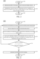
- FIG. 2 illustrates a flowchart of a first example method 200 for regulating the output power of an electronic device.
- the method 200 may be implemented, for example, by a constant power monitor circuit such as the constant power monitor circuit 100 of FIG. 1 .
- the method 200 may be implemented by the comparator 106 of the constant power monitor circuit 100.
- the comparator 106 of the constant power monitor circuit 100 As such, and for ease of explanation, reference is made in the discussion of the method 200 to various components of the constant power monitor circuit 100 of FIG. 1 .
- the method 200 begins in block 202.
- the comparator 106 measures an input voltage supplied to a monitored electronic device.
- the magnitude of the input voltage may not be constant, but may vary within some range of tolerance (e.g., plus or minus 5% of some set voltage).
- the comparator 106 dynamically adjusts a tripping current I TRIP of the monitored electronic device, in response to (e.g., based at least in part on) the measured value of the input voltage.
- the tripping current I TRIP is calculated according to EQN. 2, above.
- the tripping current I TRIP will decrease as the input voltage V IN increases.
- the tripping current I TRIP will increase as the input voltage V IN decreases
- the method 200 ends in block 208.
- FIG. 3 illustrates a flowchart of a second example method 200 for regulating the output power of an electronic device.
- the method 300 may be considered as a more detailed version of the method 200 described above.
- the method 300 may be implemented, for example, by a constant power monitor circuit such as the constant power monitor circuit 100 of FIG. 1 .
- the method 300 may be implemented by the comparator 106 of the constant power monitor circuit 100.
- the comparator 106 receives negative feedback from the feedback sub-circuit 104 (e.g., from the Zener diode 118 and Zener resistor 120). The negative feedback feeds the input voltage V IN back into the inverting input 108 of the comparator 106.
- the comparator 106 receives a signal on its threshold input 112.
- the signal on the threshold input 112 indicates a threshold voltage input level, and may be programmed by an adjustment of the limit-setting resistor 116.
- the comparator calculates the tripping current I TRIP for the monitored electronic device (i.e., the current at which the monitored electronic device should be shut down) in accordance with at least the inputs received in blocks 304-308 (i.e., the differential voltage measured across the shunt resistor 114, the negative feedback provided by the feedback sub-circuit 104, and the signal indicating the threshold input voltage.
- I TRIP is calculated according to EQN. 2.
- the comparator 106 determines whether the output current of the monitored electronic device meets or exceeds the tripping current I TRIP calculated in block 310.
- the method 300 returns to block 304, and the comparator continues to monitor the differential voltage across the shunt resistor 114.
- the method 300 proceeds to block 314.
- the comparator 106 generates a signal on its output 124 responsive to the output current meeting or exceeding the tripping current I TRIP .
- the signal may instruct the monitored electronic device to shut down.
- the method 300 ends in block 316.
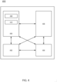
- FIG. 4 depicts a high-level block diagram of an example computer 400 that can be transformed into a machine capable of performing the functions described herein.
- the examples of the present disclosure modify the operation and functioning of the general-purpose computer to provide a constant power monitoring circuit, as disclosed herein.
- the computer 400 may be implemented in the comparator 106 of the constant power monitor circuit 100 of FIG. 1 .
- the computer 400 comprises a hardware processor element 402, e.g., a central processing unit (CPU), a microprocessor, or a multi-core processor, a memory 404, e.g., a temporary memory such as random access memory (RAM) and/or read only memory (ROM), a power monitor module 405 for monitoring the output power of an electronic device, and various input/output devices 406, e.g., storage devices, including but not limited to, a persistent memory array, a tape drive, a floppy drive, a hard disk drive or a compact disk drive, a receiver, a transmitter, a speaker, a display, a speech synthesizer, an output port, an input port and a user input device, such as a keyboard, a keypad, a mouse, a microphone, and the like.
- a hardware processor element 402 e.g., a central processing unit (CPU), a microprocessor, or a multi-core processor
- a memory 404 e.g.
- the general-purpose computer may employ a plurality of processor elements.
- one general-purpose computer is shown in the figure, if the method(s) as discussed above is implemented in a distributed or parallel manner for a particular illustrative example, i.e., the blocks of the above method(s) or the entire method(s) are implemented across multiple or parallel general-purpose computers, then the general-purpose computer of this figure is intended to represent each of those multiple general-purpose computers.
- a hardware processor can be utilized in supporting a virtualized or shared computing environment.
- the virtualized computing environment may support a virtual machine representing computers, servers, or other computing devices.
- hardware components such as hardware processors and computer-readable storage devices may be virtualized or logically represented.
- the present disclosure can be implemented by machine readable instructions and/or in a combination of machine readable instructions and hardware, e.g., using application specific integrated circuits (ASIC), a programmable logic array (PLA), including a field-programmable gate array (FPGA), or a state machine deployed on a hardware device, a general purpose computer or any other hardware equivalents, e.g., computer readable instructions pertaining to the method(s) discussed above can be used to configure a hardware processor to perform the blocks, functions and/or operations of the above disclosed methods.
- ASIC application specific integrated circuits
- PDA programmable logic array
- FPGA field-programmable gate array
- instructions and data for the present module or process 405 for monitoring the output power of an electronic device can be loaded into memory 404 and executed by hardware processor element 402 to implement the blocks, functions or operations as discussed above in connection with the methods 200 and 300.
- the module 405 may include a plurality of programming code components, including a tripping current calculation component 408 and a current comparison component 410.
- the tripping current calculation component 408 may be configured to determine at what current the constant power monitor circuit should be tripped, for example as discussed in connection with EQN. 2.
- the current comparison component 410 may be configured to determine when the output current of the monitored electronic device exceeds the tripping current calculated by the tripping current calculation component 408.
- a hardware processor executes instructions to perform "operations"
- the processor executing the machine readable instructions relating to the above described method(s) can be perceived as a programmed processor or a specialized processor.
- the present module 405 for monitoring the output power of an electronic device, including associated data structures, of the present disclosure can be stored on a tangible or physical (broadly non-transitory) computer-readable storage device or medium, e.g., volatile memory, non-volatile memory, ROM memory, RAM memory, magnetic or optical drive, device or diskette and the like.
- the computer-readable storage device may comprise any physical devices that provide the ability to store information such as data and/or instructions to be accessed by a processor or a computing device such as a computer or an application server.
Landscapes
- Engineering & Computer Science (AREA)
- Physics & Mathematics (AREA)
- General Physics & Mathematics (AREA)
- Electromagnetism (AREA)
- Radar, Positioning & Navigation (AREA)
- Automation & Control Theory (AREA)
- Computer Hardware Design (AREA)
- Microelectronics & Electronic Packaging (AREA)
- Emergency Protection Circuit Devices (AREA)
- Measurement Of Current Or Voltage (AREA)
Description
- Regulatory safety requirements specify limits and regulations in terms of output power, rather than in terms of output current or output voltage. For example, Underwriter Laboratories (UL) 62386-1 classifies electronic products as "PS2 Products" when the output power delivered by the products is limited to under one hundred watts. UL tests the PS2 circuit, and the PS2 circuit must shut down its output within five seconds of the application of a hundred watt load.
- Many PS2 devices monitor their output power by including a current sensing device in the power delivery path, and shut down when the sensed current exceeds a threshold that indicates that the output power is at or near the limit. The current (e.g., in amps) is equal to the power (e.g., in watts) divided by the voltage (e.g., in volts). Thus, as an example, a PS2 product with a 24 volt input power supply might be designed such that the current monitor circuit trips at no more than 4.16 amps (i.e., 100
watts 124 volts).
US 7821753 B2 describes a DC high power distribution assembly.WO 95/31762 A1 US 7583067 B2 describes a variable power output regulator. - The present invention is defined by the attached independent claims. Other preferred embodiments may be found in the dependent claims. The present application discloses an apparatus, comprising:an electric current monitor circuit (102), wherein the electric current monitor circuit (102) comprises:a comparator (106) having an inverting input (108) to measure a first voltage on a first side of a first resistor (114), a separate non-inverting input (110) to measure a second voltage on a second side of the first resistor (114), and an output (124);a feedback sub-circuit (104) to feed an input voltage back to the inverting input (108), wherein the feedback sub-circuit (104) comprises:a second resistor (120) coupled to the inverting input (108); and characterized in that :the apparatus further comprises a Zener diode (118) coupled between the output (124) and the second resistor (120); and the comparator (106) further comprises a threshold input (112) to receive a signal indicating a threshold voltage input level for a monitored electronic device. Further more the present application discloses a method, comprising measuring an input voltage supplied to an electronic device sensed by an inverting input (108) and a non-inverting input (110) of a comparator by measuring a first voltage on a first side of a first resistor (114) using the inverting input (108), and measuring a second voltage on a second side of the first resistor (114) using the non-inverting input (110); and characterized in that the method further comprises:dynamically adjusting a value of a threshold output current at which the electronic device shuts down in response to a value of the input voltage based on feedback from a feedback sub-circuit (104) comprising a second resistor (120) coupled to the inverting input (108) and a Zener diode (118) coupled between an output (124) of the comparator (106) and the second resistor (120); wherein the dynamically adjusting comprises computing the value of the output current based at least in part on a differential voltage measured across the first resistor (114) of a current monitor circuit, a negative feedback provided to the inverting input (108) of the current monitor circuit, and a signal indicating a threshold input voltage.The present application discloses as well a non-transitory machine-readable storage medium encoded with instructions executable by a processor, the machine-readable storage medium comprising instructions to measure an input voltage supplied to an electronic device sensed by an inverting input (108) and a non-inverting input (110) of a comparator by measuring a first voltage on a first side of a first resistor (114) using the inverting input (108), and measuring a second voltage on a second side of the first resistor (114) using the non-inverting input (110); and characterized in that the machine-readable medium further comprises:instructions to dynamically adjust a value of a threshold output current at which the electronic device shuts down in response to a value of the input voltage based on feedback from a feedback sub-circuit (104) comprising a second resistor (120) coupled to the inverting input (108) and a Zener diode (118) coupled between an output (124) of the comparator (106) and the second resistor (120); andthe instructions to dynamically adjust comprise instructions to compute the value of the output current based at least in part on a differential voltage measured across the first resistor (114) of a current monitor circuit, a negative feedback provided to the inverting input (108) of the current monitor circuit, and a signal indicating a threshold input (112) voltage.
-
-
FIGs. 1A and1B illustrate examples of constant power monitor circuit of the present disclosure; -
FIG. 2 illustrates a flowchart of a first example method for regulating the output power of an electrical device; -
FIG. 3 illustrates a flowchart of a second example method for regulating the output power of an electronic device and -
FIG. 4 depicts a high-level block diagram of an example computer that can be transformed into a machine capable of performing the functions described herein. - As discussed above, many PS2 devices monitor their output power by including a current sensing device in the power delivery path, and shut down when the sensed current exceeds a threshold that indicates that the output power is at or near the limit. For example, a PS2 product with a 24 volt input power supply might be designed such that the current monitor circuit trips at no more than 4.16 amps (i.e., 100 watts / 24 volts). However, this design does not account for voltage tolerances in the input power supply, and thus may unnecessarily reduce the available power to downstream devices.
- As an example, if the 24 volt input power supply has a tolerance of plus or minus 5%, then designing for the highest possible input voltage would trip the current monitor circuit at 3.97 amps (i.e., 100 watts / 25.2 volts), which may be insufficient to power downstream devices. For instance, if the input power supply actually receives the lowest possible input voltage (i.e., 22.8 volts in this example), then the output power when the current monitor trips at 3.97 amps would be 90.5 watts (i.e., 22.8 volts x 3.97 amps). Thus, if the downstream device consumes more than 90.5 watts of power, but less than 100 watts, during normal operation, then the PS2 product could not meet design constraints while simultaneously compensating for the tolerances in the input power supply.
- Examples of the present disclosure describe a constant power monitor circuit to compensate for tolerances in an input voltage by providing negative feedback to the inverting input of the constant current monitor circuit. In one example, the negative feedback is provided using a resistor and a Zener diode. In particular, as the input voltage increases, the resistor and Zener diode will operate to decrease the tripping current of the constant current monitor circuit. Conversely, as the input voltage decreases, the tripping current will increase. Thus, the tripping current changes dynamically in response to the magnitude of the input voltage, ensuring that downstream devices receive adequate power in a safe and reliable manner. Moreover, the disclosure provides a way to monitor and regulate output power autonomously by the monitor, without additional processing by a controlling device.
-
FIG. 1A illustrates an example of constantpower monitor circuit 100 of the present disclosure. Theexample circuit 100 may be used to monitor and regulate the output power produced by a monitored device, such as a PS2 device. To this end, theexample circuit 100 generally comprises an electriccurrent monitor circuit 102 and afeedback sub-circuit 104. - The electric
current monitor circuit 102 includes acomparator 106 having aninverting input 108, anon-inverting input 110, and anoutput 124. The invertinginput 108 and thenon-inverting input 110 sense the voltage on opposite sides of ashunt resistor 114, thereby allowing thecomparator 106 to measure the differential voltage developed across theshunt resistor 114 when current flows through theshunt resistor 114. - The
feedback sub-circuit 104 feeds the input voltage back into the invertinginput 108 of thecomparator 106. In one example illustrated in greater detail inFIG. 1B , thefeedback sub-circuit 104 includes a Zener diode and a resistor. - In operation, the
comparator 106 compares the voltage across the shunt resistor 114to a threshold voltage input level. When the voltage across theshunt resistor 114 meets or exceeds the threshold voltage input level, thecomparator 106 "trips," or generates a signal on itsoutput 124 that may be used to regulate the power output of a monitored device. As described in further detail in connection withFIG. 1B , the inclusion of thefeedback sub-circuit 104 compensates for tolerance variations of the input voltage by allowing the current at which the electriccurrent monitor circuit 102 trips to adjust dynamically in response to the input voltage. -
FIG. 1B illustrates a more detailed version of the example of constantpower monitor circuit 100 ofFIG. 1A . Identical reference numerals are used, where appropriate, to indicate components that are the same as inFIG. 1A . Thus, for example, theexample circuit 100 ofFIG. 1B generally comprises an electriccurrent monitor circuit 102 and afeedback sub-circuit 104. - The electric
current monitor circuit 102 includes acomparator 106 having aninverting input 108, anon-inverting input 110, and athreshold input 112. The invertinginput 108 and thenon-inverting input 110 sense the voltage on opposite sides of ashunt resistor 114, thereby allowing thecomparator 106 to measure the differential voltage VRS developed across theshunt resistor 114 when current flows through theshunt resistor 114. Anadditional feedback resistor 122 is positioned in series with theshunt resistor 114, between theshunt resistor 114 and the invertinginput 108 of thecomparator 106, in order to divide down the input voltage VIN from a monitored device as discussed further below. Thethreshold input 112 receives a signal indicating a threshold voltage input level. In one example, threshold voltage input level is programmable by adjusting a limit-setting resistor 116. - The
feedback sub-circuit 104 includes a Zenerdiode 118 and aresistor 120, referred to herein as a "Zener resistor" due to its coupling with the Zenerdiode 118. Together, the Zenerdiode 118 and the Zenerresistor 120 feed the input voltage VIN back into the invertinginput 108 of thecomparator 106. In one example, the Zenerdiode 118 has a reverse breakdown voltage (or "Zener voltage," i.e., the voltage at which current is permitted to flow from the cathode to the anode of the Zener diode 118) lower than the input voltage VIN. In a further example, the reverse breakdown voltage is three to seven volts lower than the input voltage VIN, in order to bias the Zenerdiode 118. - In operation, the
comparator 106 compares the voltage VRS across theshunt resistor 114 to the threshold voltage input level indicated by the signal on thethreshold input 112. When the voltage VRS across theshunt resistor 114 meets or exceeds the threshold voltage input level, thecomparator 106 "trips," or generates a signal on itsoutput 124 that may be used to regulate the power output of a monitored device. - Without the addition of the
feedback sub-circuit 104, the electriccurrent monitor circuit 102 would trip at a constant current ITRIP given by:
- Where 20 µA is assumed to be the current generated by an internal current source, RLIMIT is the resistance value of the limit-setting
resistor 116, and RS is the resistance value of theshunt resistor 114. However, with the addition of thefeedback sub-circuit 104, ITRIP becomes:
- Where RD is the resistance value of the
feedback resistor 122, RZ is the resistance value of theZener resistor 120, and VZK is the voltage across theZener diode 118. - From EQN. 2, it can be seen that the current ITRIP to trip the
circuit 100 decreases as the input voltage VIN increases. Conversely, the current ITRIP to trip thecircuit 100 increases as the input voltage VIN decreases. Thus, the inclusion of thefeedback sub-circuit 104 compensates for the tolerance variations of the input voltage VIN by allowing the current at which the electriccurrent monitor circuit 102 trips to adjust dynamically in response to the input voltage VIN. - In order to cover the range of the input voltage VIN tolerance as completely as possible, the resistance value of the
Zener resistor 120 may be calculated as follows:
circuit 100 is configured to trip. - Referring back to the example 24 volt power supply with the plus or minus 5% tolerance, a corresponding example power monitor circuit may be implemented with an 18 volt (2% tolerance) Zener diode and configured to trip at an output power of 96 watts. Based on EQN. 3, and with a 50 ohm resistor value for the feedback resistor and a 30 milliohm resistor value for the shunt resistor, the resistor value of the Zener resistor would be approximately 10 kiloohms. The electric current monitor in this case would be set for a threshold voltage VT of:

- Where Iz is the current flowing to the Zener diode. Thus, based on EQN. 4, the threshold voltage VT of the example circuit would be set to 150 millivolts. Where the threshold voltage is controlled by adjusting a limit-setting resistor, the resistor value RLIMIT of the limit-setting resistor may be set to the threshold voltage VT divided by the current generated by an internal current source. Thus, for a 20 µA internal current source, RLIMIT would be 7.5 killoohms.
- Table 1, below, illustrates the tripping power (i.e., the output power at which the constant power monitor circuit trips) for the low, nominal, and high values of the example 24 volt input power supply with the plus or minus 5% tolerance.
Table 1 Input Voltage Level VIN (volts) ITRIP (amps) PTRIP (watts) Low 22.8 4.14 94.49 Nominal 24.0 4.01 96.12 High 25.2 3.87 97.42 - The values shown in Table 1 were calculated accounting for a 2% tolerance in the 18 volt Zener diode. Even with an input voltage tolerance of plus or minus 5%, the tripping power (PTRIP) exhibits a very small variation of plus or minus 1.6%. Thus, the power tolerance window is very small in comparison to the input voltage tolerance window.
-
FIG. 2 illustrates a flowchart of afirst example method 200 for regulating the output power of an electronic device. Themethod 200 may be implemented, for example, by a constant power monitor circuit such as the constantpower monitor circuit 100 ofFIG. 1 . In a more specific example, themethod 200 may be implemented by thecomparator 106 of the constantpower monitor circuit 100. As such, and for ease of explanation, reference is made in the discussion of themethod 200 to various components of the constantpower monitor circuit 100 ofFIG. 1 . - The
method 200 begins inblock 202. Inblock 204, thecomparator 106 measures an input voltage supplied to a monitored electronic device. The magnitude of the input voltage may not be constant, but may vary within some range of tolerance (e.g., plus or minus 5% of some set voltage). - In
block 206, thecomparator 106 dynamically adjusts a tripping current ITRIP of the monitored electronic device, in response to (e.g., based at least in part on) the measured value of the input voltage. In one example, the tripping current ITRIP is calculated according to EQN. 2, above. Thus, the tripping current ITRIP will decrease as the input voltage VIN increases. Conversely, the tripping current ITRIP will increase as the input voltage VIN decreases - The
method 200 ends inblock 208. -
FIG. 3 illustrates a flowchart of asecond example method 200 for regulating the output power of an electronic device. Themethod 300 may be considered as a more detailed version of themethod 200 described above. Thus, themethod 300 may be implemented, for example, by a constant power monitor circuit such as the constantpower monitor circuit 100 ofFIG. 1 . In a more specific example, themethod 300 may be implemented by thecomparator 106 of the constantpower monitor circuit 100. As such, and for ease of explanation, reference is made in the discussion of themethod 300 to various components of the constantpower monitor circuit 100 ofFIG. 1 . - The
method 300 begins inblock 302. Inblock 304, thecomparator 106 measures the differential voltage VRS developed across theshunt resistor 114, in response to the input voltage VIN being supplied to the monitored electronic device. In particular, the voltages on opposite sides of theshunt resistor 114 are sensed by the invertinginput 108 and thenon-inverting input 110 of thecomparator 106. The voltage measured by the invertinginput 108 is divided down by thefeedback resistor 122. - In
block 306, thecomparator 106 receives negative feedback from the feedback sub-circuit 104 (e.g., from theZener diode 118 and Zener resistor 120). The negative feedback feeds the input voltage VIN back into the invertinginput 108 of thecomparator 106. - In
block 308, thecomparator 106 receives a signal on itsthreshold input 112. The signal on thethreshold input 112 indicates a threshold voltage input level, and may be programmed by an adjustment of the limit-settingresistor 116. - In
block 310, the comparator calculates the tripping current ITRIP for the monitored electronic device (i.e., the current at which the monitored electronic device should be shut down) in accordance with at least the inputs received in blocks 304-308 (i.e., the differential voltage measured across theshunt resistor 114, the negative feedback provided by thefeedback sub-circuit 104, and the signal indicating the threshold input voltage. In one example, ITRIP is calculated according to EQN. 2. - In
block 312, thecomparator 106 determines whether the output current of the monitored electronic device meets or exceeds the tripping current ITRIP calculated inblock 310. - If the
comparator 106 concludes inblock 312 that the output current of the monitored electronic device is below the tripping current ITRIP, then themethod 300 returns to block 304, and the comparator continues to monitor the differential voltage across theshunt resistor 114. - If, however, the comparator concludes in
block 312 that the output current of the monitored electronic device meets or exceeds the tripping current ITRIP, then themethod 300 proceeds to block 314. Inblock 314, thecomparator 106 generates a signal on itsoutput 124 responsive to the output current meeting or exceeding the tripping current ITRIP. The signal may instruct the monitored electronic device to shut down. - The
method 300 ends inblock 316. -
FIG. 4 depicts a high-level block diagram of anexample computer 400 that can be transformed into a machine capable of performing the functions described herein. Notably, no computer or machine currently exists that performs the functions as described herein. As a result, the examples of the present disclosure modify the operation and functioning of the general-purpose computer to provide a constant power monitoring circuit, as disclosed herein. Thus, thecomputer 400 may be implemented in thecomparator 106 of the constantpower monitor circuit 100 ofFIG. 1 . - As depicted in
FIG. 4 , thecomputer 400 comprises ahardware processor element 402, e.g., a central processing unit (CPU), a microprocessor, or a multi-core processor, amemory 404, e.g., a temporary memory such as random access memory (RAM) and/or read only memory (ROM), apower monitor module 405 for monitoring the output power of an electronic device, and various input/output devices 406, e.g., storage devices, including but not limited to, a persistent memory array, a tape drive, a floppy drive, a hard disk drive or a compact disk drive, a receiver, a transmitter, a speaker, a display, a speech synthesizer, an output port, an input port and a user input device, such as a keyboard, a keypad, a mouse, a microphone, and the like. - Although one processor element is shown, it should be noted that the general-purpose computer may employ a plurality of processor elements. Furthermore, although one general-purpose computer is shown in the figure, if the method(s) as discussed above is implemented in a distributed or parallel manner for a particular illustrative example, i.e., the blocks of the above method(s) or the entire method(s) are implemented across multiple or parallel general-purpose computers, then the general-purpose computer of this figure is intended to represent each of those multiple general-purpose computers. Furthermore, a hardware processor can be utilized in supporting a virtualized or shared computing environment. The virtualized computing environment may support a virtual machine representing computers, servers, or other computing devices. In such virtualized virtual machines, hardware components such as hardware processors and computer-readable storage devices may be virtualized or logically represented.
- It should be noted that the present disclosure can be implemented by machine readable instructions and/or in a combination of machine readable instructions and hardware, e.g., using application specific integrated circuits (ASIC), a programmable logic array (PLA), including a field-programmable gate array (FPGA), or a state machine deployed on a hardware device, a general purpose computer or any other hardware equivalents, e.g., computer readable instructions pertaining to the method(s) discussed above can be used to configure a hardware processor to perform the blocks, functions and/or operations of the above disclosed methods.
- In one example, instructions and data for the present module or
process 405 for monitoring the output power of an electronic device, e.g., machine readable instructions can be loaded intomemory 404 and executed byhardware processor element 402 to implement the blocks, functions or operations as discussed above in connection with themethods module 405 may include a plurality of programming code components, including a trippingcurrent calculation component 408 and acurrent comparison component 410. - The tripping
current calculation component 408 may be configured to determine at what current the constant power monitor circuit should be tripped, for example as discussed in connection with EQN. 2. Thecurrent comparison component 410 may be configured to determine when the output current of the monitored electronic device exceeds the tripping current calculated by the trippingcurrent calculation component 408. - Furthermore, when a hardware processor executes instructions to perform "operations", this could include the hardware processor performing the operations directly and/or facilitating, directing, or cooperating with another hardware device or component, e.g., a co-processor and the like, to perform the operations.
- The processor executing the machine readable instructions relating to the above described method(s) can be perceived as a programmed processor or a specialized processor. As such, the
present module 405 for monitoring the output power of an electronic device, including associated data structures, of the present disclosure can be stored on a tangible or physical (broadly non-transitory) computer-readable storage device or medium, e.g., volatile memory, non-volatile memory, ROM memory, RAM memory, magnetic or optical drive, device or diskette and the like. More specifically, the computer-readable storage device may comprise any physical devices that provide the ability to store information such as data and/or instructions to be accessed by a processor or a computing device such as a computer or an application server.
Claims (12)
- An apparatus, comprising:an electric current monitor circuit (102), wherein the electric current monitor circuit (102) comprises:
a comparator (106) having an inverting input (108) to measure a first voltage on a first side of a first resistor (114), a separate non-inverting input (110) to measure a second voltage on a second side of the first resistor (114), and an output (124);a feedback sub-circuit (104) to feed an input voltage back to the inverting input (108), wherein the feedback sub-circuit (104) comprises:characterized in that:
a second resistor (120) coupled to the inverting input (108); and
the apparatus further comprises a Zener diode (118) coupled between the output (124) and the second resistor (120); and
the comparator (106) further comprises a threshold input (112) to receive a signal indicating a threshold voltage input level for a monitored electronic device. - The apparatus of claim 1, wherein the threshold input (112) is coupled to a third resistor (116).
- The apparatus of claim 2, wherein a resistance of the third resistor (116) is programmable to adjust the threshold voltage input level.
- The apparatus of claim 1, further comprising:
a third resistor (122) positioned between the first resistor (114) and the inverting input (108). - The apparatus of claim 1, wherein a reverse breakdown voltage of the Zener diode (118) is programmed to be lower than the input voltage.
- The apparatus of claim 5, wherein the reverse breakdown voltage is three to seven volts lower than the input voltage.
- The apparatus of claim 1, wherein the apparatus monitors the output power of an electronic device.
- The apparatus of claim 7, wherein the electronic device is a PS2 device.
- A method, comprising:
measuring an input voltage supplied to an electronic device sensed by an inverting input (108) and a non-inverting input (110) of a comparator by measuring a first voltage on a first side of a first resistor (114) using the inverting input (108), and measuring a second voltage on a second side of the first resistor (114) using the non-inverting input (110); andcharacterized in that the method further comprises:
dynamically adjusting a value of a threshold output current at which the electronic device shuts down in response to a value of the input voltage based on feedback from a feedback sub-circuit (104) comprising a second resistor (120) coupled to the inverting input (108) and a Zener diode (118) coupled between an output (124) of the comparator (106) and the second resistor (120);wherein the dynamically adjusting comprises computing the value of the output current based at least in part on a differential voltage measured across the first resistor (114) of a current monitor circuit, a negative feedback provided to the inverting input (108) of the current monitor circuit, and a signal indicating a threshold input voltage. - The method of claim 9, further comprising:measuring a value of a present output current of the electronic device; andgenerating a signal to shut down the electronic device when the present output current meets the threshold output current.
- A non-transitory machine-readable storage medium encoded with instructions executable by a processor, the machine-readable storage medium comprising:
instructions to measure an input voltage supplied to an electronic device sensed by an inverting input (108) and a non-inverting input (110) of a comparator by measuring a first voltage on a first side of a first resistor (114) using the inverting input (108), and measuring a second voltage on a second side of the first resistor (114) using the non-inverting input (110); and
characterized in that the machine-readable medium further comprises:instructions to dynamically adjust a value of a threshold output current at which the electronic device shuts down in response to a value of the input voltage based on feedback from a feedback sub-circuit (104) comprising a second resistor (120) coupled to the inverting input (108) and a Zener diode (118) coupled between an output (124) of the comparator (106) and the second resistor (120); andthe instructions to dynamically adjust comprise instructions to compute the value of the output current based at least in part on a differential voltage measured across the first resistor (114) of a current monitor circuit, a negative feedback provided to the inverting input (108) of the current monitor circuit, and a signal indicating a threshold input (112) voltage. - The non-transitory machine-readable storage medium of claim 11, further comprising:instructions to measure a value of a present output current of the electronic device; andinstructions to generate a signal to shut down the electronic device when the present output current meets the threshold output current.
Applications Claiming Priority (1)
| Application Number | Priority Date | Filing Date | Title |
|---|---|---|---|
| PCT/US2016/043258 WO2018017088A1 (en) | 2016-07-21 | 2016-07-21 | Circuit for dynamically adjusting a threshold output current based on an input voltage |
Publications (3)
| Publication Number | Publication Date |
|---|---|
| EP3433694A1 EP3433694A1 (en) | 2019-01-30 |
| EP3433694A4 EP3433694A4 (en) | 2020-02-26 |
| EP3433694B1 true EP3433694B1 (en) | 2024-01-03 |
Family
ID=60993318
Family Applications (1)
| Application Number | Title | Priority Date | Filing Date |
|---|---|---|---|
| EP16909681.5A Active EP3433694B1 (en) | 2016-07-21 | 2016-07-21 | Circuit for dynamically adjusting a threshold output current based on an input voltage |
Country Status (4)
| Country | Link |
|---|---|
| US (1) | US10739800B2 (en) |
| EP (1) | EP3433694B1 (en) |
| CN (1) | CN109154841B (en) |
| WO (1) | WO2018017088A1 (en) |
Families Citing this family (4)
| Publication number | Priority date | Publication date | Assignee | Title |
|---|---|---|---|---|
| CN108155638B (en) * | 2016-12-05 | 2023-12-05 | 珠海格力电器股份有限公司 | Control equipment and control methods of DC microgrid, DC microgrid system |
| WO2020027814A1 (en) * | 2018-07-31 | 2020-02-06 | Hewlett-Packard Development Company, L.P. | Operating modes of a computer display |
| US11509230B2 (en) * | 2019-11-07 | 2022-11-22 | Texas Instruments Incorporated | Power stage controller for switching converter with clamp |
| US11693382B2 (en) * | 2020-12-22 | 2023-07-04 | Fisher Controls International Llc | Methods and apparatus to adjust operation of a fluid flow control assembly |
Family Cites Families (43)
| Publication number | Priority date | Publication date | Assignee | Title |
|---|---|---|---|---|
| US4253055A (en) * | 1977-02-22 | 1981-02-24 | American Optical Corporation | Adjustable switching current regulator |
| DE2933874C2 (en) * | 1978-08-24 | 1986-07-17 | Hochiki Corp., Tokio/Tokyo | Sensing device for sensing temperature differences between two points |
| US4398711A (en) * | 1979-12-31 | 1983-08-16 | Ncr Corporation | Currency dispenser monitor |
| US5010279A (en) * | 1985-08-26 | 1991-04-23 | Lathom Michael S | Switched capacitive ballasts for discharge lamps |
| US4870532A (en) * | 1988-08-24 | 1989-09-26 | Westinghouse Electric Corp. | Electric circuit for operating trip circuit of a circuit breaker |
| DE69223530T2 (en) * | 1991-02-22 | 1998-04-09 | Matsushita Electric Ind Co Ltd | Power supply unit |
| RU2011213C1 (en) * | 1991-09-03 | 1994-04-15 | Киевское производственное объединение "Электронмаш" | Electric power supply with protection |
| DE4131170A1 (en) * | 1991-09-19 | 1993-03-25 | Telefunken Electronic Gmbh | DEVICE FOR GENERATING INTERMEDIATE VOLTAGES |
| JP3110242B2 (en) * | 1994-03-24 | 2000-11-20 | 三菱電機株式会社 | Ignition detector |
| CN1076291C (en) * | 1994-04-14 | 2001-12-19 | 富士通坦株式会社 | vehicle anti-theft device |
| US5563500A (en) * | 1994-05-16 | 1996-10-08 | Thomson Consumer Electronics, Inc. | Voltage regulator having complementary type transistor |
| EP0860762A3 (en) * | 1997-02-25 | 1999-04-07 | TEMIC TELEFUNKEN microelectronic GmbH | Circuit and method for generating a DC output voltage |
| US6301133B1 (en) * | 1999-04-07 | 2001-10-09 | Astec International Limited | Power supply system with ORing element and control circuit |
| US6157555A (en) * | 1999-11-09 | 2000-12-05 | International Business Machines Corporation | Current limiter responsive to changing parallel power supply capacity |
| JP2001216033A (en) * | 2000-02-02 | 2001-08-10 | Yazaki Corp | Power supply control device and power supply control method |
| JP2002315201A (en) | 2001-04-12 | 2002-10-25 | Nec Miyagi Ltd | Discharge prevention circuit |
| US7123136B2 (en) * | 2003-10-06 | 2006-10-17 | Anden Co., Ltd. | Indicator system having multiple LEDs |
| US7342761B2 (en) * | 2003-12-16 | 2008-03-11 | Rockwell Automation Technologies, Inc. | Apparatus and method for limiting application of electrical power to a load |
| US7526659B2 (en) * | 2005-02-01 | 2009-04-28 | Hewlett-Packard Development Company, L.P. | Systems and methods for controlling use of power in a computer system |
| US7304462B2 (en) * | 2005-02-02 | 2007-12-04 | Power-One, Inc. | Compensated droop method for paralleling of power supplies (C-droop method) |
| JP4829622B2 (en) * | 2005-02-17 | 2011-12-07 | キヤノン株式会社 | Switching power supply, electronic device equipped with switching power supply, recording device equipped with switching power supply |
| US7095217B1 (en) | 2005-03-31 | 2006-08-22 | O2Micro International Limited | Method circuitry and electronic device for controlling a variable output dc power source |
| US7609499B2 (en) * | 2005-05-05 | 2009-10-27 | Seagate Technology Llc | Active current limiting circuit |
| US7619391B2 (en) * | 2005-10-20 | 2009-11-17 | Defond Components Limited | Electrical appliance with battery protection |
| US7274999B1 (en) * | 2006-03-10 | 2007-09-25 | Atmel Corporation | Brownout detector system and method |
| US7821753B2 (en) * | 2007-01-18 | 2010-10-26 | Alcatel-Lucent Usa Inc. | DC high power distribution assembly |
| US8649144B2 (en) * | 2007-02-05 | 2014-02-11 | Semiconductor Components Industries, Llc | Method of forming an over-voltage protection circuit and structure therefor |
| US7746613B1 (en) * | 2007-02-28 | 2010-06-29 | Maxim Integrated Products, Inc. | Method and apparatus for providing an adaptive current limiter |
| US8143878B2 (en) * | 2008-12-12 | 2012-03-27 | Infineon Technologies Ag | Starter circuit, bandgap circuit and monitoring circuit |
| CN101907900A (en) | 2010-08-04 | 2010-12-08 | 深圳和而泰智能控制股份有限公司 | Wide-voltage constant-power control circuit and hair straightener |
| JP2013013288A (en) | 2011-06-30 | 2013-01-17 | Shindengen Electric Mfg Co Ltd | Constant current power supply device |
| US8575863B2 (en) | 2011-11-08 | 2013-11-05 | Atmel Corporation | Color correcting device driver |
| CN202738176U (en) | 2012-06-11 | 2013-02-13 | 鸿富锦精密工业(深圳)有限公司 | An electronic apparatus and a control circuit of the electronic apparatus |
| TWI467540B (en) * | 2012-12-14 | 2015-01-01 | Upi Semiconductor Corp | Reference voltage generator of gate driving circuit and reference voltage generating method |
| WO2014121662A1 (en) | 2013-02-08 | 2014-08-14 | 东林科技股份有限公司 | Constant-power supply apparatus and constant-power output control method |
| US8830776B1 (en) * | 2013-03-15 | 2014-09-09 | Freescale Semiconductor, Inc. | Negative charge pump regulation |
| TWI548184B (en) | 2014-09-05 | 2016-09-01 | 緯創資通股份有限公司 | Protection device and method for electronic device |
| US10256809B2 (en) * | 2015-08-24 | 2019-04-09 | Ruizhang Technology Limited Company | Power-on reset circuit |
| WO2017075111A1 (en) * | 2015-10-26 | 2017-05-04 | Dialog Semiconductor Inc. | Switching power converter with zero current at startup |
| KR102594096B1 (en) * | 2016-02-23 | 2023-10-26 | 삼성디스플레이 주식회사 | Short detection circuit and display device including the same |
| EP3442811A4 (en) * | 2016-04-13 | 2019-11-27 | Hewlett-Packard Development Company, L.P. | DEVICES COMPRISING TWO RELAYS AT CURRENT THRESHOLD |
| CN106708155B (en) * | 2016-11-22 | 2017-12-26 | 成都芯源系统有限公司 | Integrated circuit and circuit characteristic adjusting method thereof |
| US20180145668A1 (en) * | 2016-11-22 | 2018-05-24 | Mosway Technologies Limited | Voltage clamping circuit |
-
2016
- 2016-07-21 EP EP16909681.5A patent/EP3433694B1/en active Active
- 2016-07-21 CN CN201680085223.XA patent/CN109154841B/en not_active Expired - Fee Related
- 2016-07-21 US US16/097,528 patent/US10739800B2/en not_active Expired - Fee Related
- 2016-07-21 WO PCT/US2016/043258 patent/WO2018017088A1/en not_active Ceased
Also Published As
| Publication number | Publication date |
|---|---|
| US10739800B2 (en) | 2020-08-11 |
| US20190146529A1 (en) | 2019-05-16 |
| CN109154841A (en) | 2019-01-04 |
| WO2018017088A1 (en) | 2018-01-25 |
| CN109154841B (en) | 2021-04-02 |
| EP3433694A4 (en) | 2020-02-26 |
| EP3433694A1 (en) | 2019-01-30 |
Similar Documents
| Publication | Publication Date | Title |
|---|---|---|
| CN112930506B (en) | Adaptive Gate Bias Field Effect Transistor for Low Dropout Regulators | |
| US10969848B2 (en) | System power monitor | |
| US10739800B2 (en) | Regulating an output power of a monitored electronic device | |
| US9645594B2 (en) | Voltage regulator with dropout detector and bias current limiter and associated methods | |
| US11422579B2 (en) | Low dropout control for light load quiescent current reduction | |
| CN100511939C (en) | Voltage regulator | |
| TWI604292B (en) | Voltage regulator | |
| US9455628B2 (en) | Voltage regulator with overshoot suppression circuit and capability to stop overshoot suppression | |
| CN102597900A (en) | low dropout regulator | |
| US20140117957A1 (en) | Voltage regulator | |
| US11003201B1 (en) | Low quiescent current low-dropout regulator (LDO) | |
| US11294412B2 (en) | Apparatuses and methods involving switching between dual inputs of power amplification circuitry | |
| US7583067B2 (en) | Variable power output regulator | |
| US10998722B2 (en) | Load-sharing power system | |
| US10942535B2 (en) | Operational amplifier with current limiting circuitry | |
| KR101659901B1 (en) | Voltage regulator having over-current protection circuit | |
| US10013010B1 (en) | Voltage droop mitigation circuit for power supply network | |
| US20200081470A1 (en) | Voltage regulator | |
| US10476299B2 (en) | DC link voltage control | |
| DE112020004210T5 (en) | force sensing circuit | |
| KR101796769B1 (en) | Capacitorless low drop out regulator and controlling circuit therefor | |
| CN109947161B (en) | Power supply system and control method of power supply system | |
| US20180191317A1 (en) | Differential sensing circuit of a floating voltage source | |
| US20070080670A1 (en) | Power dissipation management in linear regulators | |
| US8301929B2 (en) | System and method for dynamic power regulator for power supply output adjustment |
Legal Events
| Date | Code | Title | Description |
|---|---|---|---|
| STAA | Information on the status of an ep patent application or granted ep patent |
Free format text: STATUS: THE INTERNATIONAL PUBLICATION HAS BEEN MADE |
|
| PUAI | Public reference made under article 153(3) epc to a published international application that has entered the european phase |
Free format text: ORIGINAL CODE: 0009012 |
|
| STAA | Information on the status of an ep patent application or granted ep patent |
Free format text: STATUS: REQUEST FOR EXAMINATION WAS MADE |
|
| 17P | Request for examination filed |
Effective date: 20181023 |
|
| AK | Designated contracting states |
Kind code of ref document: A1 Designated state(s): AL AT BE BG CH CY CZ DE DK EE ES FI FR GB GR HR HU IE IS IT LI LT LU LV MC MK MT NL NO PL PT RO RS SE SI SK SM TR |
|
| AX | Request for extension of the european patent |
Extension state: BA ME |
|
| RAP1 | Party data changed (applicant data changed or rights of an application transferred) |
Owner name: HEWLETT-PACKARD DEVELOPMENT COMPANY, L.P. |
|
| DAV | Request for validation of the european patent (deleted) | ||
| DAX | Request for extension of the european patent (deleted) | ||
| RIC1 | Information provided on ipc code assigned before grant |
Ipc: G05F 1/573 20060101AFI20190923BHEP |
|
| A4 | Supplementary search report drawn up and despatched |
Effective date: 20200127 |
|
| RIC1 | Information provided on ipc code assigned before grant |
Ipc: G05F 1/573 20060101AFI20200121BHEP |
|
| STAA | Information on the status of an ep patent application or granted ep patent |
Free format text: STATUS: EXAMINATION IS IN PROGRESS |
|
| 17Q | First examination report despatched |
Effective date: 20211011 |
|
| GRAP | Despatch of communication of intention to grant a patent |
Free format text: ORIGINAL CODE: EPIDOSNIGR1 |
|
| STAA | Information on the status of an ep patent application or granted ep patent |
Free format text: STATUS: GRANT OF PATENT IS INTENDED |
|
| INTG | Intention to grant announced |
Effective date: 20230912 |
|
| GRAS | Grant fee paid |
Free format text: ORIGINAL CODE: EPIDOSNIGR3 |
|
| GRAA | (expected) grant |
Free format text: ORIGINAL CODE: 0009210 |
|
| STAA | Information on the status of an ep patent application or granted ep patent |
Free format text: STATUS: THE PATENT HAS BEEN GRANTED |
|
| AK | Designated contracting states |
Kind code of ref document: B1 Designated state(s): AL AT BE BG CH CY CZ DE DK EE ES FI FR GB GR HR HU IE IS IT LI LT LU LV MC MK MT NL NO PL PT RO RS SE SI SK SM TR |
|
| REG | Reference to a national code |
Ref country code: GB Ref legal event code: FG4D |
|
| REG | Reference to a national code |
Ref country code: DE Ref legal event code: R096 Ref document number: 602016085199 Country of ref document: DE |
|
| REG | Reference to a national code |
Ref country code: CH Ref legal event code: EP |
|
| REG | Reference to a national code |
Ref country code: IE Ref legal event code: FG4D |
|
| REG | Reference to a national code |
Ref country code: LT Ref legal event code: MG9D |
|
| PG25 | Lapsed in a contracting state [announced via postgrant information from national office to epo] |
Ref country code: ES Free format text: LAPSE BECAUSE OF FAILURE TO SUBMIT A TRANSLATION OF THE DESCRIPTION OR TO PAY THE FEE WITHIN THE PRESCRIBED TIME-LIMIT Effective date: 20240103 |
|
| PG25 | Lapsed in a contracting state [announced via postgrant information from national office to epo] |
Ref country code: ES Free format text: LAPSE BECAUSE OF FAILURE TO SUBMIT A TRANSLATION OF THE DESCRIPTION OR TO PAY THE FEE WITHIN THE PRESCRIBED TIME-LIMIT Effective date: 20240103 |
|
| REG | Reference to a national code |
Ref country code: NL Ref legal event code: MP Effective date: 20240103 |
|
| REG | Reference to a national code |
Ref country code: AT Ref legal event code: MK05 Ref document number: 1647454 Country of ref document: AT Kind code of ref document: T Effective date: 20240103 |
|
| PG25 | Lapsed in a contracting state [announced via postgrant information from national office to epo] |
Ref country code: NL Free format text: LAPSE BECAUSE OF FAILURE TO SUBMIT A TRANSLATION OF THE DESCRIPTION OR TO PAY THE FEE WITHIN THE PRESCRIBED TIME-LIMIT Effective date: 20240103 |
|
| PG25 | Lapsed in a contracting state [announced via postgrant information from national office to epo] |
Ref country code: NL Free format text: LAPSE BECAUSE OF FAILURE TO SUBMIT A TRANSLATION OF THE DESCRIPTION OR TO PAY THE FEE WITHIN THE PRESCRIBED TIME-LIMIT Effective date: 20240103 |
|
| PG25 | Lapsed in a contracting state [announced via postgrant information from national office to epo] |
Ref country code: IS Free format text: LAPSE BECAUSE OF FAILURE TO SUBMIT A TRANSLATION OF THE DESCRIPTION OR TO PAY THE FEE WITHIN THE PRESCRIBED TIME-LIMIT Effective date: 20240503 |
|
| PG25 | Lapsed in a contracting state [announced via postgrant information from national office to epo] |
Ref country code: LT Free format text: LAPSE BECAUSE OF FAILURE TO SUBMIT A TRANSLATION OF THE DESCRIPTION OR TO PAY THE FEE WITHIN THE PRESCRIBED TIME-LIMIT Effective date: 20240103 |
|
| PG25 | Lapsed in a contracting state [announced via postgrant information from national office to epo] |
Ref country code: GR Free format text: LAPSE BECAUSE OF FAILURE TO SUBMIT A TRANSLATION OF THE DESCRIPTION OR TO PAY THE FEE WITHIN THE PRESCRIBED TIME-LIMIT Effective date: 20240404 |
|
| PG25 | Lapsed in a contracting state [announced via postgrant information from national office to epo] |
Ref country code: RS Free format text: LAPSE BECAUSE OF FAILURE TO SUBMIT A TRANSLATION OF THE DESCRIPTION OR TO PAY THE FEE WITHIN THE PRESCRIBED TIME-LIMIT Effective date: 20240403 Ref country code: HR Free format text: LAPSE BECAUSE OF FAILURE TO SUBMIT A TRANSLATION OF THE DESCRIPTION OR TO PAY THE FEE WITHIN THE PRESCRIBED TIME-LIMIT Effective date: 20240103 |
|
| PG25 | Lapsed in a contracting state [announced via postgrant information from national office to epo] |
Ref country code: CZ Free format text: LAPSE BECAUSE OF FAILURE TO SUBMIT A TRANSLATION OF THE DESCRIPTION OR TO PAY THE FEE WITHIN THE PRESCRIBED TIME-LIMIT Effective date: 20240103 Ref country code: AT Free format text: LAPSE BECAUSE OF FAILURE TO SUBMIT A TRANSLATION OF THE DESCRIPTION OR TO PAY THE FEE WITHIN THE PRESCRIBED TIME-LIMIT Effective date: 20240103 |
|
| PG25 | Lapsed in a contracting state [announced via postgrant information from national office to epo] |
Ref country code: RS Free format text: LAPSE BECAUSE OF FAILURE TO SUBMIT A TRANSLATION OF THE DESCRIPTION OR TO PAY THE FEE WITHIN THE PRESCRIBED TIME-LIMIT Effective date: 20240403 Ref country code: NO Free format text: LAPSE BECAUSE OF FAILURE TO SUBMIT A TRANSLATION OF THE DESCRIPTION OR TO PAY THE FEE WITHIN THE PRESCRIBED TIME-LIMIT Effective date: 20240403 Ref country code: LT Free format text: LAPSE BECAUSE OF FAILURE TO SUBMIT A TRANSLATION OF THE DESCRIPTION OR TO PAY THE FEE WITHIN THE PRESCRIBED TIME-LIMIT Effective date: 20240103 Ref country code: IS Free format text: LAPSE BECAUSE OF FAILURE TO SUBMIT A TRANSLATION OF THE DESCRIPTION OR TO PAY THE FEE WITHIN THE PRESCRIBED TIME-LIMIT Effective date: 20240503 Ref country code: HR Free format text: LAPSE BECAUSE OF FAILURE TO SUBMIT A TRANSLATION OF THE DESCRIPTION OR TO PAY THE FEE WITHIN THE PRESCRIBED TIME-LIMIT Effective date: 20240103 Ref country code: GR Free format text: LAPSE BECAUSE OF FAILURE TO SUBMIT A TRANSLATION OF THE DESCRIPTION OR TO PAY THE FEE WITHIN THE PRESCRIBED TIME-LIMIT Effective date: 20240404 Ref country code: CZ Free format text: LAPSE BECAUSE OF FAILURE TO SUBMIT A TRANSLATION OF THE DESCRIPTION OR TO PAY THE FEE WITHIN THE PRESCRIBED TIME-LIMIT Effective date: 20240103 Ref country code: BG Free format text: LAPSE BECAUSE OF FAILURE TO SUBMIT A TRANSLATION OF THE DESCRIPTION OR TO PAY THE FEE WITHIN THE PRESCRIBED TIME-LIMIT Effective date: 20240103 Ref country code: AT Free format text: LAPSE BECAUSE OF FAILURE TO SUBMIT A TRANSLATION OF THE DESCRIPTION OR TO PAY THE FEE WITHIN THE PRESCRIBED TIME-LIMIT Effective date: 20240103 |
|
| PG25 | Lapsed in a contracting state [announced via postgrant information from national office to epo] |
Ref country code: PL Free format text: LAPSE BECAUSE OF FAILURE TO SUBMIT A TRANSLATION OF THE DESCRIPTION OR TO PAY THE FEE WITHIN THE PRESCRIBED TIME-LIMIT Effective date: 20240103 Ref country code: PT Free format text: LAPSE BECAUSE OF FAILURE TO SUBMIT A TRANSLATION OF THE DESCRIPTION OR TO PAY THE FEE WITHIN THE PRESCRIBED TIME-LIMIT Effective date: 20240503 |
|
| PG25 | Lapsed in a contracting state [announced via postgrant information from national office to epo] |
Ref country code: SE Free format text: LAPSE BECAUSE OF FAILURE TO SUBMIT A TRANSLATION OF THE DESCRIPTION OR TO PAY THE FEE WITHIN THE PRESCRIBED TIME-LIMIT Effective date: 20240103 Ref country code: PT Free format text: LAPSE BECAUSE OF FAILURE TO SUBMIT A TRANSLATION OF THE DESCRIPTION OR TO PAY THE FEE WITHIN THE PRESCRIBED TIME-LIMIT Effective date: 20240503 Ref country code: PL Free format text: LAPSE BECAUSE OF FAILURE TO SUBMIT A TRANSLATION OF THE DESCRIPTION OR TO PAY THE FEE WITHIN THE PRESCRIBED TIME-LIMIT Effective date: 20240103 Ref country code: LV Free format text: LAPSE BECAUSE OF FAILURE TO SUBMIT A TRANSLATION OF THE DESCRIPTION OR TO PAY THE FEE WITHIN THE PRESCRIBED TIME-LIMIT Effective date: 20240103 |
|
| REG | Reference to a national code |
Ref country code: DE Ref legal event code: R097 Ref document number: 602016085199 Country of ref document: DE |
|
| PG25 | Lapsed in a contracting state [announced via postgrant information from national office to epo] |
Ref country code: DK Free format text: LAPSE BECAUSE OF FAILURE TO SUBMIT A TRANSLATION OF THE DESCRIPTION OR TO PAY THE FEE WITHIN THE PRESCRIBED TIME-LIMIT Effective date: 20240103 |
|
| PG25 | Lapsed in a contracting state [announced via postgrant information from national office to epo] |
Ref country code: SM Free format text: LAPSE BECAUSE OF FAILURE TO SUBMIT A TRANSLATION OF THE DESCRIPTION OR TO PAY THE FEE WITHIN THE PRESCRIBED TIME-LIMIT Effective date: 20240103 |
|
| PG25 | Lapsed in a contracting state [announced via postgrant information from national office to epo] |
Ref country code: EE Free format text: LAPSE BECAUSE OF FAILURE TO SUBMIT A TRANSLATION OF THE DESCRIPTION OR TO PAY THE FEE WITHIN THE PRESCRIBED TIME-LIMIT Effective date: 20240103 |
|
| PG25 | Lapsed in a contracting state [announced via postgrant information from national office to epo] |
Ref country code: SK Free format text: LAPSE BECAUSE OF FAILURE TO SUBMIT A TRANSLATION OF THE DESCRIPTION OR TO PAY THE FEE WITHIN THE PRESCRIBED TIME-LIMIT Effective date: 20240103 |
|
| PG25 | Lapsed in a contracting state [announced via postgrant information from national office to epo] |
Ref country code: SM Free format text: LAPSE BECAUSE OF FAILURE TO SUBMIT A TRANSLATION OF THE DESCRIPTION OR TO PAY THE FEE WITHIN THE PRESCRIBED TIME-LIMIT Effective date: 20240103 Ref country code: SK Free format text: LAPSE BECAUSE OF FAILURE TO SUBMIT A TRANSLATION OF THE DESCRIPTION OR TO PAY THE FEE WITHIN THE PRESCRIBED TIME-LIMIT Effective date: 20240103 Ref country code: RO Free format text: LAPSE BECAUSE OF FAILURE TO SUBMIT A TRANSLATION OF THE DESCRIPTION OR TO PAY THE FEE WITHIN THE PRESCRIBED TIME-LIMIT Effective date: 20240103 Ref country code: EE Free format text: LAPSE BECAUSE OF FAILURE TO SUBMIT A TRANSLATION OF THE DESCRIPTION OR TO PAY THE FEE WITHIN THE PRESCRIBED TIME-LIMIT Effective date: 20240103 Ref country code: DK Free format text: LAPSE BECAUSE OF FAILURE TO SUBMIT A TRANSLATION OF THE DESCRIPTION OR TO PAY THE FEE WITHIN THE PRESCRIBED TIME-LIMIT Effective date: 20240103 |
|
| PLBE | No opposition filed within time limit |
Free format text: ORIGINAL CODE: 0009261 |
|
| STAA | Information on the status of an ep patent application or granted ep patent |
Free format text: STATUS: NO OPPOSITION FILED WITHIN TIME LIMIT |
|
| PG25 | Lapsed in a contracting state [announced via postgrant information from national office to epo] |
Ref country code: IT Free format text: LAPSE BECAUSE OF FAILURE TO SUBMIT A TRANSLATION OF THE DESCRIPTION OR TO PAY THE FEE WITHIN THE PRESCRIBED TIME-LIMIT Effective date: 20240103 |
|
| 26N | No opposition filed |
Effective date: 20241007 |
|
| PG25 | Lapsed in a contracting state [announced via postgrant information from national office to epo] |
Ref country code: IT Free format text: LAPSE BECAUSE OF FAILURE TO SUBMIT A TRANSLATION OF THE DESCRIPTION OR TO PAY THE FEE WITHIN THE PRESCRIBED TIME-LIMIT Effective date: 20240103 |
|
| REG | Reference to a national code |
Ref country code: DE Ref legal event code: R119 Ref document number: 602016085199 Country of ref document: DE |
|
| PG25 | Lapsed in a contracting state [announced via postgrant information from national office to epo] |
Ref country code: MC Free format text: LAPSE BECAUSE OF FAILURE TO SUBMIT A TRANSLATION OF THE DESCRIPTION OR TO PAY THE FEE WITHIN THE PRESCRIBED TIME-LIMIT Effective date: 20240103 |
|
| REG | Reference to a national code |
Ref country code: CH Ref legal event code: PL |
|
| PG25 | Lapsed in a contracting state [announced via postgrant information from national office to epo] |
Ref country code: LU Free format text: LAPSE BECAUSE OF NON-PAYMENT OF DUE FEES Effective date: 20240721 |
|
| GBPC | Gb: european patent ceased through non-payment of renewal fee |
Effective date: 20240721 |
|
| PG25 | Lapsed in a contracting state [announced via postgrant information from national office to epo] |
Ref country code: LU Free format text: LAPSE BECAUSE OF NON-PAYMENT OF DUE FEES Effective date: 20240721 |
|
| PG25 | Lapsed in a contracting state [announced via postgrant information from national office to epo] |
Ref country code: DE Free format text: LAPSE BECAUSE OF NON-PAYMENT OF DUE FEES Effective date: 20250201 |
|
| PG25 | Lapsed in a contracting state [announced via postgrant information from national office to epo] |
Ref country code: CH Free format text: LAPSE BECAUSE OF NON-PAYMENT OF DUE FEES Effective date: 20240731 Ref country code: BE Free format text: LAPSE BECAUSE OF NON-PAYMENT OF DUE FEES Effective date: 20240731 Ref country code: SI Free format text: LAPSE BECAUSE OF FAILURE TO SUBMIT A TRANSLATION OF THE DESCRIPTION OR TO PAY THE FEE WITHIN THE PRESCRIBED TIME-LIMIT Effective date: 20240103 |
|
| PG25 | Lapsed in a contracting state [announced via postgrant information from national office to epo] |
Ref country code: FR Free format text: LAPSE BECAUSE OF NON-PAYMENT OF DUE FEES Effective date: 20240731 |
|
| PG25 | Lapsed in a contracting state [announced via postgrant information from national office to epo] |
Ref country code: GB Free format text: LAPSE BECAUSE OF NON-PAYMENT OF DUE FEES Effective date: 20240721 |
|
| REG | Reference to a national code |
Ref country code: BE Ref legal event code: MM Effective date: 20240731 |
|
| PG25 | Lapsed in a contracting state [announced via postgrant information from national office to epo] |
Ref country code: IE Free format text: LAPSE BECAUSE OF NON-PAYMENT OF DUE FEES Effective date: 20240721 |
|
| PG25 | Lapsed in a contracting state [announced via postgrant information from national office to epo] |
Ref country code: FI Free format text: LAPSE BECAUSE OF FAILURE TO SUBMIT A TRANSLATION OF THE DESCRIPTION OR TO PAY THE FEE WITHIN THE PRESCRIBED TIME-LIMIT Effective date: 20240103 |
|
| PG25 | Lapsed in a contracting state [announced via postgrant information from national office to epo] |
Ref country code: CY Free format text: LAPSE BECAUSE OF FAILURE TO SUBMIT A TRANSLATION OF THE DESCRIPTION OR TO PAY THE FEE WITHIN THE PRESCRIBED TIME-LIMIT; INVALID AB INITIO Effective date: 20160721 |
|
| PG25 | Lapsed in a contracting state [announced via postgrant information from national office to epo] |
Ref country code: HU Free format text: LAPSE BECAUSE OF FAILURE TO SUBMIT A TRANSLATION OF THE DESCRIPTION OR TO PAY THE FEE WITHIN THE PRESCRIBED TIME-LIMIT; INVALID AB INITIO Effective date: 20160721 |