EP3432456A1 - Switched-capacitor converters with capacitor pre-charging - Google Patents
Switched-capacitor converters with capacitor pre-charging Download PDFInfo
- Publication number
- EP3432456A1 EP3432456A1 EP18184336.8A EP18184336A EP3432456A1 EP 3432456 A1 EP3432456 A1 EP 3432456A1 EP 18184336 A EP18184336 A EP 18184336A EP 3432456 A1 EP3432456 A1 EP 3432456A1
- Authority
- EP
- European Patent Office
- Prior art keywords
- capacitor
- legs
- input
- switched
- controller
- Prior art date
- Legal status (The legal status is an assumption and is not a legal conclusion. Google has not performed a legal analysis and makes no representation as to the accuracy of the status listed.)
- Granted
Links
Images





Classifications
-
- H—ELECTRICITY
- H02—GENERATION; CONVERSION OR DISTRIBUTION OF ELECTRIC POWER
- H02M—APPARATUS FOR CONVERSION BETWEEN AC AND AC, BETWEEN AC AND DC, OR BETWEEN DC AND DC, AND FOR USE WITH MAINS OR SIMILAR POWER SUPPLY SYSTEMS; CONVERSION OF DC OR AC INPUT POWER INTO SURGE OUTPUT POWER; CONTROL OR REGULATION THEREOF
- H02M3/00—Conversion of DC power input into DC power output
- H02M3/02—Conversion of DC power input into DC power output without intermediate conversion into AC
- H02M3/04—Conversion of DC power input into DC power output without intermediate conversion into AC by static converters
- H02M3/06—Conversion of DC power input into DC power output without intermediate conversion into AC by static converters using resistors or capacitors, e.g. potential divider
- H02M3/07—Conversion of DC power input into DC power output without intermediate conversion into AC by static converters using resistors or capacitors, e.g. potential divider using capacitors charged and discharged alternately by semiconductor devices with control electrode, e.g. charge pumps
-
- H—ELECTRICITY
- H02—GENERATION; CONVERSION OR DISTRIBUTION OF ELECTRIC POWER
- H02M—APPARATUS FOR CONVERSION BETWEEN AC AND AC, BETWEEN AC AND DC, OR BETWEEN DC AND DC, AND FOR USE WITH MAINS OR SIMILAR POWER SUPPLY SYSTEMS; CONVERSION OF DC OR AC INPUT POWER INTO SURGE OUTPUT POWER; CONTROL OR REGULATION THEREOF
- H02M1/00—Details of apparatus for conversion
- H02M1/32—Means for protecting converters other than automatic disconnection
-
- H—ELECTRICITY
- H02—GENERATION; CONVERSION OR DISTRIBUTION OF ELECTRIC POWER
- H02M—APPARATUS FOR CONVERSION BETWEEN AC AND AC, BETWEEN AC AND DC, OR BETWEEN DC AND DC, AND FOR USE WITH MAINS OR SIMILAR POWER SUPPLY SYSTEMS; CONVERSION OF DC OR AC INPUT POWER INTO SURGE OUTPUT POWER; CONTROL OR REGULATION THEREOF
- H02M1/00—Details of apparatus for conversion
- H02M1/36—Means for starting or stopping converters
-
- H—ELECTRICITY
- H02—GENERATION; CONVERSION OR DISTRIBUTION OF ELECTRIC POWER
- H02M—APPARATUS FOR CONVERSION BETWEEN AC AND AC, BETWEEN AC AND DC, OR BETWEEN DC AND DC, AND FOR USE WITH MAINS OR SIMILAR POWER SUPPLY SYSTEMS; CONVERSION OF DC OR AC INPUT POWER INTO SURGE OUTPUT POWER; CONTROL OR REGULATION THEREOF
- H02M3/00—Conversion of DC power input into DC power output
- H02M3/02—Conversion of DC power input into DC power output without intermediate conversion into AC
- H02M3/04—Conversion of DC power input into DC power output without intermediate conversion into AC by static converters
- H02M3/06—Conversion of DC power input into DC power output without intermediate conversion into AC by static converters using resistors or capacitors, e.g. potential divider
- H02M3/07—Conversion of DC power input into DC power output without intermediate conversion into AC by static converters using resistors or capacitors, e.g. potential divider using capacitors charged and discharged alternately by semiconductor devices with control electrode, e.g. charge pumps
- H02M3/073—Charge pumps of the Schenkel-type
-
- H—ELECTRICITY
- H02—GENERATION; CONVERSION OR DISTRIBUTION OF ELECTRIC POWER
- H02M—APPARATUS FOR CONVERSION BETWEEN AC AND AC, BETWEEN AC AND DC, OR BETWEEN DC AND DC, AND FOR USE WITH MAINS OR SIMILAR POWER SUPPLY SYSTEMS; CONVERSION OF DC OR AC INPUT POWER INTO SURGE OUTPUT POWER; CONTROL OR REGULATION THEREOF
- H02M3/00—Conversion of DC power input into DC power output
- H02M3/02—Conversion of DC power input into DC power output without intermediate conversion into AC
- H02M3/04—Conversion of DC power input into DC power output without intermediate conversion into AC by static converters
- H02M3/10—Conversion of DC power input into DC power output without intermediate conversion into AC by static converters using discharge tubes with control electrode or semiconductor devices with control electrode
- H02M3/145—Conversion of DC power input into DC power output without intermediate conversion into AC by static converters using discharge tubes with control electrode or semiconductor devices with control electrode using devices of a triode or transistor type requiring continuous application of a control signal
- H02M3/155—Conversion of DC power input into DC power output without intermediate conversion into AC by static converters using discharge tubes with control electrode or semiconductor devices with control electrode using devices of a triode or transistor type requiring continuous application of a control signal using semiconductor devices only
- H02M3/156—Conversion of DC power input into DC power output without intermediate conversion into AC by static converters using discharge tubes with control electrode or semiconductor devices with control electrode using devices of a triode or transistor type requiring continuous application of a control signal using semiconductor devices only with automatic control of output voltage or current, e.g. switching regulators
- H02M3/158—Conversion of DC power input into DC power output without intermediate conversion into AC by static converters using discharge tubes with control electrode or semiconductor devices with control electrode using devices of a triode or transistor type requiring continuous application of a control signal using semiconductor devices only with automatic control of output voltage or current, e.g. switching regulators including plural semiconductor devices as final control devices for a single load
- H02M3/1588—Conversion of DC power input into DC power output without intermediate conversion into AC by static converters using discharge tubes with control electrode or semiconductor devices with control electrode using devices of a triode or transistor type requiring continuous application of a control signal using semiconductor devices only with automatic control of output voltage or current, e.g. switching regulators including plural semiconductor devices as final control devices for a single load comprising at least one synchronous rectifier element
-
- H—ELECTRICITY
- H03—ELECTRONIC CIRCUITRY
- H03H—IMPEDANCE NETWORKS, e.g. RESONANT CIRCUITS; RESONATORS
- H03H19/00—Networks using time-varying elements, e.g. N-path filters
- H03H19/004—Switched capacitor networks
-
- H—ELECTRICITY
- H05—ELECTRIC TECHNIQUES NOT OTHERWISE PROVIDED FOR
- H05B—ELECTRIC HEATING; ELECTRIC LIGHT SOURCES NOT OTHERWISE PROVIDED FOR; CIRCUIT ARRANGEMENTS FOR ELECTRIC LIGHT SOURCES, IN GENERAL
- H05B45/00—Circuit arrangements for operating light-emitting diodes [LED]
- H05B45/30—Driver circuits
- H05B45/37—Converter circuits
- H05B45/3725—Switched mode power supply [SMPS]
-
- H—ELECTRICITY
- H10—SEMICONDUCTOR DEVICES; ELECTRIC SOLID-STATE DEVICES NOT OTHERWISE PROVIDED FOR
- H10D—INORGANIC ELECTRIC SEMICONDUCTOR DEVICES
- H10D84/00—Integrated devices formed in or on semiconductor substrates that comprise only semiconducting layers, e.g. on Si wafers or on GaAs-on-Si wafers
- H10D84/80—Integrated devices formed in or on semiconductor substrates that comprise only semiconducting layers, e.g. on Si wafers or on GaAs-on-Si wafers characterised by the integration of at least one component covered by groups H10D12/00 or H10D30/00, e.g. integration of IGFETs
- H10D84/82—Integrated devices formed in or on semiconductor substrates that comprise only semiconducting layers, e.g. on Si wafers or on GaAs-on-Si wafers characterised by the integration of at least one component covered by groups H10D12/00 or H10D30/00, e.g. integration of IGFETs of only field-effect components
- H10D84/83—Integrated devices formed in or on semiconductor substrates that comprise only semiconducting layers, e.g. on Si wafers or on GaAs-on-Si wafers characterised by the integration of at least one component covered by groups H10D12/00 or H10D30/00, e.g. integration of IGFETs of only field-effect components of only insulated-gate FETs [IGFET]
-
- H—ELECTRICITY
- H10—SEMICONDUCTOR DEVICES; ELECTRIC SOLID-STATE DEVICES NOT OTHERWISE PROVIDED FOR
- H10W—GENERIC PACKAGES, INTERCONNECTIONS, CONNECTORS OR OTHER CONSTRUCTIONAL DETAILS OF DEVICES COVERED BY CLASS H10
- H10W20/00—Interconnections in chips, wafers or substrates
- H10W20/40—Interconnections external to wafers or substrates, e.g. back-end-of-line [BEOL] metallisations or vias connecting to gate electrodes
- H10W20/495—Capacitive arrangements or effects of, or between wiring layers
- H10W20/496—Capacitor integral with wiring layers
Definitions
- the present application relates to switched-capacitor converters, in particular startup control for switched-capacitor converters.
- Switched-capacitor converters are a class of voltage converters which provide energy transfer and voltage conversion using capacitors.
- Each leg of a switched-capacitor converter includes a capacitor, and a switch device is connected to each leg for controlling charging of the capacitors.
- some of the legs also include inductors which makes those legs resonant.
- different groups of the converter legs are coupled to different branches of a rectifier at the output.
- the different groups of converter legs are switched alternately to transfer energy from the input to the output.
- the rectifier such as a half-bridge rectifier, rectifies the energy transferred from the capacitors during each switching cycle.
- the rectified output can be applied directly to a load, or to another converter stage such as a buck converter, a POL (point-of-load) converter, etc.
- Initial capacitor voltages and inductor currents at startup may be either zero or different from the steady-state values, causing large spikes and inrush current which place very high stress on the switch devices, especially the switch device closest to the input, and other components.
- the inrush current should be reduced or ideally prevented.
- a shunt resistor is placed in series with the switched-capacitor converter input.
- An external switch is connected in parallel with the shunt resistor to bypass the shunt resistor during post startup operation.
- the inrush current is reduced, but the approach Is not suitable for pre-charging the capacitors during startup. Hence, a relatively high shunt value is required which makes the startup process very slow.
- An improved technique is needed for pre-charging one or more capacitors of a switched-capacitor converter.
- the converter comprises: an input; an output; a rectifier at the output; a plurality of legs coupled between the input and the rectifier, each leg comprising a capacitor, a first group of the legs being coupled to a first branch of the rectifier and a second group of the legs being coupled to a second branch of the rectifier; a switch device connected to each leg; and a controller.
- the controller is operable to alternate switching of the first and the second groups of legs after startup, to transfer energy from the input to the output during a first part of each switching cycle via the first group of legs and to ground during a second part of each switching cycle via the second group of legs.
- the controller is further operable control the switch devices during startup so that a combination of the switch devices which are normally switched in a complimentary manner after startup are on at the same time to pre-charge at least one of the capacitors.
- the converter comprises: an input; an output; a rectifier at the output; a plurality of legs coupled between the input and the rectifier, each leg comprising a capacitor, a first group of the legs being coupled to a first branch of the rectifier and a second group of the legs being coupled to a second branch of the rectifier; a switch device connected to each leg; a controller; and a current limited source coupled between the input and the plurality of legs.
- the controller is operable to alternate switching of the first and the second groups of legs after startup, to transfer energy from the input to the output during a first part of each switching cycle via the first group of legs and to ground during a second part of each switching cycle via the second group of legs.
- the current limited source is operable to pre-charge at least one of the capacitors during startup.
- the converter comprises: an input; an output; a rectifier at the output; a plurality of legs coupled between the input and the rectifier, each leg comprising a capacitor, a first group of the legs being coupled to a first branch of the rectifier and a second group of the legs being coupled to a second branch of the rectifier; a switch device connected to each leg; and a controller.
- the controller is operable to alternate switching of the first and the second groups of legs after startup, to transfer energy from the input to the output during a first part of each switching cycle via the first group of legs and to ground during a second part of each switching cycle via the second group of legs.
- the controller is further operable adjust a gate-to-source voltage applied to at least one of the switch devices during startup, to adjust an on-state resistance of the at least one switch device.
- the converter comprises: an input; an output; a rectifier at the output; a plurality of legs coupled between the input and the rectifier, each leg comprising a capacitor, a first group of the legs being coupled to a first branch of the rectifier and a second group of the legs being coupled to a second branch of the rectifier; a switch device connected to each leg; and a controller.
- the controller is operable to alternate switching of the first and the second groups of legs after startup, to transfer energy from the input to the output during a first part of each switching cycle via the first group of legs and to ground during a second part of each switching cycle via the second group of legs.
- the controller is further operable to turn each switch device on and off in succession in a burst mode during startup, starting with the switch device closest to the input and ending with the switch device furthest from the input.
- the embodiments described herein provide for pre-charging of one or more capacitors of a switched-capacitor converter during startup, such that the transition from startup to regular (post startup) operation occurs with lower stress on the switch devices and other components of the switched-capacitor converter in the shortest possible time.
- FIG. 1 illustrates an embodiment of a switched-capacitor converter 100 with capacitor pre-charging during startup.
- the switched-capacitor converter 100 has an input 102 coupled to a voltage source Vin, an output 104 coupled to a load or other converter 106, a rectifier 108 and output capacitor Cout at the output 104, and a plurality of legs coupled between the input 102 and the rectifier 108.
- the rectified output voltage Vout can be applied directly to a load or another converter stage 106 such as a buck converter, a POL (point-of-load) converter, etc.
- the input voltage Vin may range from 36 V to 54 V and the output voltage Vout may range from 6V to 9V in a multi-stage converter case.
- a controller 110 for the switched-capacitor converter 100 maintains proper switching of the converter legs to transfer energy from the input 102 to the output 104.
- Each leg of the switched-capacitor converter 100 includes a respective capacitor Cx (wherein Cx denotes an arbitrary one of the capacitors C1-C5 shown in Figure 1 ).
- Some of the legs also referred to herein as resonant legs, include an inductor Ly (wherein Ly denotes an arbitrary one of the inductors L1-L3 shown in Figure 1 ) connected to the corresponding capacitor Cy (wherein Cy denotes an arbitrary one of the capacitors C1, C3, C5 shown in Figure 1 ).
- a switch device Qx (wherein Qx denotes an arbitrary one of the switch devices Q1-Q5 shown in Figure 1 ) is connected to each leg, for controlling charging of the capacitors Cx.
- resonant leg 1 includes resonant capacitor C1 and inductor L1
- (flying) leg 2 includes flying capacitor C2
- resonant leg 3 includes resonant capacitor C3 and inductor L2
- (flying) leg 4 includes flying capacitor C4
- resonant leg 5 includes resonant capacitor C5.
- the switch devices Qx can be discrete power transistor dies (chips), integrated power stages which include at least the power transistors that form the individual switch device and the corresponding driver and control circuitry, etc.
- the (first) group of resonant legs which includes resonant capacitors C1, C3 and C5 is coupled to a first branch 112 of the rectifier 108
- the (second) group of non-resonant (flying) legs which includes flying capacitors C2 and C4 is coupled to a second branch 114 of the rectifier 108.
- the rectifier is a switched capacitor rectifier in that for each group of legs, the AC currents are in opposite phase during normal (post startup) operation. While the first group is charging during normal operation, the other group is discharging.
- the rectifier switches alternatively connect each leg to the output when the current is being discharged, and to ground when the current is charging.
- each branch 112, 114 of the rectifier 108 includes two switch devices Qm/Qn coupled as a half bridge, wherein the first branch 112 includes switches Q7, Q8 and the second branch 114 includes switches Q9, Q10.
- Other rectifier configurations are possible.
- V C5 is the voltage across capacitor C5
- V C4 is the voltage across capacitor C4
- V C3 is the voltage across capacitor C3
- V C2 is the voltage across capacitor C2
- V C1 is the voltage across capacitor C1.
- the switched-capacitor converter 100 can include any number of legs.
- the number of legs depends on the application in which the converter 100 is to be used.
- the controller 110 of the switched-capacitor converter 100 alternates switching of the first (resonant) and the second (non-resonant) groups of legs to transfer energy from the input 102 to the output 104 during post startup operation.
- switch devices Q1, Q3, Q5, Q7 and Q10 can be switched via a first PWM (pulse width modulation) signal with approximately 50% duty cycle and switch devices Q2, Q4, Q6, Q8 and Q9 can be switched via the complementary PWM signal with dead time between the PWM signals.
- the controller 110 can implement other duty cycle combinations post startup.
- the capacitor voltages V C1 , V C2 , etc. and the inductor currents i L1 , i L2 , etc. of the switched-capacitor converter 100 are either zero or different from the respective steady-state values.
- the controller 110 ensures one or more of the capacitors C1 through C5 is pre-charged during startup, by controlling the switch devices so that a combination of the switch devices which are normally switched in a complimentary manner after startup are on at the same time to pre-charge at least one of the capacitors during startup.
- the on-time of the switch devices during startup can be limited (reduced) to just enough time to charge the corresponding capacitors, thus limiting the inrush current during startup.
- switch devices Q1, Q3, Q5, Q7 and Q10 are on for a first part of each switching cycle during post startup operation and switch devices Q2, Q4, Q6, Q8 and Q9 are on for a second part of each switching cycle.
- the controller 110 can pre-charge at least resonant capacitor C1 by adapting the PWM control so that switch devices Q1 and Q8 are on at the same time during startup.
- Figure 1 shows exemplary current paths through resonant capacitors C1 and C3 during startup as thick arrows, which can be realized by appropriate control of the corresponding PWM signals.
- the controller 110 can modify the PWM control of the switch devices to limit voltage overshoot on the capacitors, e.g. based on threshold values or time criteria as described in more detail below.
- the switched-capacitor converter 100 also includes measurement circuitry 116 such as DCR sense circuitry, on-state resistance (R DSon ) measurement circuitry, comparator circuitry, etc. for sensing or estimating the voltage across each of the capacitors during startup.
- the controller 110 turns off each switch device during startup when the voltage sensed across the capacitor connected to that switch device reaches a predetermined level for that capacitor, so that the switch devices connected to the capacitors with lower predetermined levels are turned off during startup before the switch devices connected to the capacitors with higher predetermined levels.
- the controller 110 turns on switch devices Q1 through Q5, Q8 and Q10 to pre-charge capacitors C1 through C5, and then turns off switch devices Q5 through Q1 once capacitors C5 through C1 reach their desired respective levels.
- the measurement circuitry 116 can sense the voltage across resonant capacitor C1 or the switch node voltage between switch devices Q2 and Q3 for flying capacitor C2.
- the measurement circuitry 116 can sense the voltage across the other resonant capacitors in a similar manner.
- the controller 110 turns on switch devices Q1 through Q3, Q8 and Q10 to pre-charge capacitors C1, C2 and C3 which are charged at a higher level than the other capacitors.
- the controller 110 implements the PWM control of switch device Q1 at a higher frequency than the other switch devices to charge resonant capacitor C1 via inductor L1 and switch device Q8, and subsequently charge flying capacitor C2 by switch device Q10 via switch device Q8 and inductor L1.
- the controller 110 can repeat the sequence for other downstream capacitor stages, and re-charge resonant capacitor C1 as needed.
- a fourth approach involves the controller 110 setting switch devices Q2 through Q5 in the on-state to charge all capacitors simultaneously. With the fourth approach, the controller 110 can turn on switch devices Q1 and Q8 for some time and charge resonant capacitor C1 and then use other switch devices to transfer energy from capacitor C1 to the other capacitors.
- a fifth approach involves the controller 110 setting switch devices Q2 through Q5 in the on-state and switch device Q10 in the off state to charge resonant capacitors C1, C3 and C5 simultaneously. Subsequent turning off of switch device Q1 and turning on of switch devices Q2, Q4 and Q10 charges flying capacitors C2 and C4 resonantly via the inductors. The controller 110 can repeat the sequence until desired pre-charge capacitor voltage levels have been reached.
- the controller 110 turns off each switch device during startup when a timer value assigned to that switch device expires.
- the timer values correspond to respective pre-charge voltages of the capacitors connected to the switch devices.
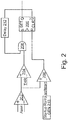
- Figure 2 illustrates an embodiment of timing circuitry included in or associated with the controller 110 for implementing capacitor pre-charging during startup.
- the output Q of a flip-flop 200 controls a logical gate function between the PWM signal for switch device Q1 and the gate driver of switch device Q1. If the output Q of the flip-flop 200 is low, the gate of switch device Q1 is always low. If the output Q of the flip-flop 200 is high, the gate of switch device Q1 follows the corresponding PWM signal issued by the controller 110.
- Sensed current or capacitor voltage signal Asen which can be generated e.g.
- inductor current sensing of inductor L1 is input to a current sense comparator 202 and compared to a maximum reference value THR at the positive input of a second comparator 204. This is for resetting a logic gate 206 which re-enables the output Q of the flip-flop 200.
- the current sense comparator output also is input to a reset comparator 208 that compares the sensed current value to an ever increasing startup current value (softstart) at the negative input of the reset comparator 208.
- the startup current value can be generated by a ramp generator 210. When the current value output by the current sense comparator 202 is higher than the output of the ramp generator 210, the flip-flop 200 switches off and the gate of switch device Q1 goes low. After a delay 212, the flip-flop 200 can be reset when the current level falls below the reference level of the reset comparator 208.
- FIG 3 illustrates another embodiment of a switched-capacitor converter 300 with capacitor pre-charging during startup.
- the switched-capacitor converter embodiment shown in Figure 3 is similar to the embodiment shown in Figure 1 .
- the switched-capacitor converter 300 shown in Figure 3 also includes a shunt resistor Rshunt between the input Vin and the legs of the switched-capacitor converter 300.
- the shunt resistor Rshunt controls the inrush current during startup.
- the shunt resistor Rshunt is bypassed by a switch device 302 after startup.
- the bypass switch device 302 can be turned on automatically, or by the controller 110. Any of the capacitor pre-charging embodiments described above in connection with Figures 1 and 2 can be implemented in the embodiment of Figure 3 , and are not repeated here.
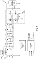
- FIG 4 illustrates yet another embodiment of a switched-capacitor converter 400 with capacitor pre-charging during startup.
- the switched-capacitor converter embodiment shown in Figure 4 is similar to the embodiment shown in Figure 1 .
- the switched-capacitor converter 400 shown in Figure 4 also includes a current limited source 402 coupled between the input Vin and the legs of the switched-capacitor converter 400.
- the current limited source 402 is a circuit having an element that limits the maximum (inrush) current during startup, while at least one of the capacitors is pre-charging. Any circuit that has an upper limit on the current which depends on the voltage across the circuit can be used as the current limited source 402, such as, but not limited to a resistor, a MOSFET in saturation, a BJT in linear mode operation, etc.
- the current limited source 402 pre-charges at least the capacitor C1 closest to the input Vin during startup and stops charging capacitor C1 when the voltage across capacitor C1 reaches a predetermined level. Any of the capacitor pre-charging embodiments described above in connection with Figures 1 through 3 can be implemented in conjunction with the current limited source embodiment of Figure 4 , and are not repeated here. Described next are other embodiments of the current limited source 402.
- Figures 5 and 6 illustrate the current limited source 402 implemented as a resistor divider R1/R2 ( Figure 5 ) or R1/R2/R3 ( Figure 6 ) and a diode D1 ( Figure 5 ) or D1/D2 ( Figure 6 ) connecting the input Vin to the capacitor C1 closest to the input.
- the resistor divider / diode arrangement can pre-charge resonant capacitor C1 by itself as shown in Figure 5 , or flying capacitors C2 and C4 at different voltages as shown in Figure 6 .
- Figures 7 and 8 illustrate additional resistor divider / diode implementations of the current limited source 402, wherein the resistor divider goes into Vout directly instead of ground (at the risk of direct connection from Vin to Vout).
- a buffer FET or NPN bipolar transistor 500 / 502 can be used with a current limiting resistor Rlimit to reduce the power loss in the resistor divider while limiting the inrush current during startup.
- Each current limiting resistor Rlimit can be in series with the source/emitter or drain/collector of the corresponding buffer FET / NPN bipolar transistor 500 / 502.
- Figure 9 illustrates the current limited source 402 implemented as a charge pump that pre-charges one or more of the capacitors to a certain level.
- the charge pump is connected to at least the capacitor C1 closest to the input, and includes e.g. a resistor divider R1/R2, transistor 600, diode D, and capacitor C.
- the charge pump can be autonomous in that the charge pump can be disabled responsive to the voltage reaching a certain level, or the controller 110 can disable the charge pump.
- the current limited source 402 can provide a single tap between the input Vin and the capacitor C1 closest to the input.
- the pre-charging sequence includes the controller 110 turning on switch devices Q8 and Q10 to prevent overcharging of the output Vout, which is not likely to happen since preferably Cout >> C1.
- the controller 110 turns on switch device Q2 through Q5 to charge capacitors C2 through C5, and then successively turns off switch devices Q5 through Q2 to limit the voltage on capacitors C5 through C2.
- the time constant is set mostly by flying capacitors C2 and C4, so the initial voltage on resonant capacitor C1 should not matter and the controller 110 can set the on-time for switch device Q1 to ensure proper pre-charging.
- the controller 110 can exit startup and enter normal (post startup) operation.
- the current limited source 402 has dual taps between the input Vin and the capacitor C1 closest to the input.
- the pre-charging sequence includes the controller 110 turning on switch devices Q8 and Q10 to prevent overcharging of the output Vout.
- Resonant capacitors C1 and C3 are pre-charged through body diodes of switch devices Q2 and Q4, to values slightly below the voltages across flying capacitors C2 and C4, respectively.
- the controller 110 turns off switch device Q10, and then turns on switch devices Q2 and Q4 to pre-charge resonant C1 and C3 to about the same level as flying capacitors C2 and C4, respectively.
- This pre-charging is damped by the current limited source 402, so the timing need not be precisely determined. If needed, the controller 110 can pulse switch devices Q2 and Q4 to limit the currents which pre-charge flying capacitors C2 and C4, respectively.
- FIG 10 illustrates still another embodiment of a switched-capacitor converter 700 with capacitor pre-charging during startup.
- the switched-capacitor converter embodiment shown in Figure 10 is similar to the embodiment shown in Figure 1 .
- the controller 110 of the switched-capacitor converter 700 shown in Figure 10 includes circuitry 702 for adjusting the gate-to-source voltage (Vgs) applied to at least the switch device Q1 closest to the input Vin, to adjust the on-state resistance (R DSon ) of the at least one switch device Q1 during startup.
- Vgs gate-to-source voltage
- R DSon on-state resistance
- the shunt value is a gate resistance value controlled by the on-state resistance (R DSon ) of at least the switch device Q1 closest to the input Vin.
- the gate-to-source voltage Vgs of switch device Q1 can be reduced to increase on-state resistance during startup.
- Figure 11 illustrates one embodiment of the gate-to-source voltage Vgs control technique, for adjusting the on-state resistance R DSon of at least the switch device Q1 closest to the input Vin.
- one or more n-channel MOSFETs 800 and a gate shunt resistor R are provided between the gate driver 802 for switch device Q1 and the gate input of switch device Q1.
- Other auxiliary devices such as p-Channel MOSFETs for example, can be used instead.
- a charge pump 804 and related diode and capacitor circuitry DBoot / CBoot power the gate driver 802 during startup.
- the gate-to-source voltage Vgs of switch device Q1 is controlled based on the desired amount of (gate) shunt resistance.
- the gate-to-source voltage Vgs can be controlled by adding more or less resistance at the gate of switch device Q1.
- the bypass switch 800 is on and a lower Vgs is applied to switch device Q1.
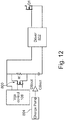
- Figure 12 illustrates another embodiment of the gate-to-source voltage Vgs control technique, for adjusting the on-state resistance R DSon of at least the switch device Q1 closest to the input Vin.
- the embodiment shown in Figure 12 is similar to the embodiment shown in Figure 11 .
- the gate shunt resistor R and corresponding switch device 800 is placed before the gate driver 802 for switch device Q1, so that the gate driver 802 is between switch device Q1 and the gate shunt resistor R.
- FIG 13 illustrates another embodiment of the capacitor pre-charging process implemented by the switched-capacitor converter controller 110.
- the controller 110 turns each switch device on and off in succession in a burst mode during startup.
- the controller 110 starts with the switch device Q1 closest to the input Vin and ends with the switch device Q6 furthest from the input Vin.
- the on-time of each switch device is labelled 'Tonx' in Figure 13 .
- inductor L1 and resonant capacitor C1 are energized through switch device Q1 for a certain period (Ton1) and then the energy is transferred downstream to the rest of the legs.
- the controller 110 can repeat the burst mode at least one time during startup, to ensure all leg capacitors are pre-charged to the desired respective levels.
Landscapes
- Engineering & Computer Science (AREA)
- Power Engineering (AREA)
- Dc-Dc Converters (AREA)
Abstract
Description
- The present application relates to switched-capacitor converters, in particular startup control for switched-capacitor converters.
- Switched-capacitor converters are a class of voltage converters which provide energy transfer and voltage conversion using capacitors. Each leg of a switched-capacitor converter includes a capacitor, and a switch device is connected to each leg for controlling charging of the capacitors. In some implementations, some of the legs also include inductors which makes those legs resonant. In either case, different groups of the converter legs are coupled to different branches of a rectifier at the output. The different groups of converter legs are switched alternately to transfer energy from the input to the output. The rectifier, such as a half-bridge rectifier, rectifies the energy transferred from the capacitors during each switching cycle. The rectified output can be applied directly to a load, or to another converter stage such as a buck converter, a POL (point-of-load) converter, etc.
- Initial capacitor voltages and inductor currents at startup may be either zero or different from the steady-state values, causing large spikes and inrush current which place very high stress on the switch devices, especially the switch device closest to the input, and other components. To optimize the size of the capacitors, inductors and switch devices of a switched-capacitor converter, the inrush current should be reduced or ideally prevented. Conventionally, a shunt resistor is placed in series with the switched-capacitor converter input. An external switch is connected in parallel with the shunt resistor to bypass the shunt resistor during post startup operation. The inrush current is reduced, but the approach Is not suitable for pre-charging the capacitors during startup. Hence, a relatively high shunt value is required which makes the startup process very slow. An improved technique is needed for pre-charging one or more capacitors of a switched-capacitor converter.
- According to an embodiment of a switched-capacitor converter, the converter comprises: an input; an output; a rectifier at the output; a plurality of legs coupled between the input and the rectifier, each leg comprising a capacitor, a first group of the legs being coupled to a first branch of the rectifier and a second group of the legs being coupled to a second branch of the rectifier; a switch device connected to each leg; and a controller. The controller is operable to alternate switching of the first and the second groups of legs after startup, to transfer energy from the input to the output during a first part of each switching cycle via the first group of legs and to ground during a second part of each switching cycle via the second group of legs. The controller is further operable control the switch devices during startup so that a combination of the switch devices which are normally switched in a complimentary manner after startup are on at the same time to pre-charge at least one of the capacitors.
- According to another embodiment of a switched-capacitor converter, the converter comprises: an input; an output; a rectifier at the output; a plurality of legs coupled between the input and the rectifier, each leg comprising a capacitor, a first group of the legs being coupled to a first branch of the rectifier and a second group of the legs being coupled to a second branch of the rectifier; a switch device connected to each leg; a controller; and a current limited source coupled between the input and the plurality of legs. The controller is operable to alternate switching of the first and the second groups of legs after startup, to transfer energy from the input to the output during a first part of each switching cycle via the first group of legs and to ground during a second part of each switching cycle via the second group of legs. The current limited source is operable to pre-charge at least one of the capacitors during startup.
- According to yet another embodiment of a switched-capacitor converter, the converter comprises: an input; an output; a rectifier at the output; a plurality of legs coupled between the input and the rectifier, each leg comprising a capacitor, a first group of the legs being coupled to a first branch of the rectifier and a second group of the legs being coupled to a second branch of the rectifier; a switch device connected to each leg; and a controller. The controller is operable to alternate switching of the first and the second groups of legs after startup, to transfer energy from the input to the output during a first part of each switching cycle via the first group of legs and to ground during a second part of each switching cycle via the second group of legs. The controller is further operable adjust a gate-to-source voltage applied to at least one of the switch devices during startup, to adjust an on-state resistance of the at least one switch device.
- According to still another embodiment of a switched-capacitor converter, the converter comprises: an input; an output; a rectifier at the output; a plurality of legs coupled between the input and the rectifier, each leg comprising a capacitor, a first group of the legs being coupled to a first branch of the rectifier and a second group of the legs being coupled to a second branch of the rectifier; a switch device connected to each leg; and a controller. The controller is operable to alternate switching of the first and the second groups of legs after startup, to transfer energy from the input to the output during a first part of each switching cycle via the first group of legs and to ground during a second part of each switching cycle via the second group of legs. The controller is further operable to turn each switch device on and off in succession in a burst mode during startup, starting with the switch device closest to the input and ending with the switch device furthest from the input.
- Those skilled in the art will recognize additional features and advantages upon reading the following detailed description, and upon viewing the accompanying drawings.
- The elements of the drawings are not necessarily to scale relative to each other. Like reference numerals designate corresponding similar parts. The features of the various illustrated embodiments can be combined unless they exclude each other. Embodiments are depicted in the drawings and are detailed in the description which follows.
-
Figure 1 illustrates a block diagram of an embodiment of a switched-capacitor converter with capacitor pre-charging. -
Figure 2 illustrates a block diagram of an embodiment of timing circuitry for implementing capacitor pre-charging during startup. -
Figure 3 illustrates a block diagram of another embodiment of a switched-capacitor converter with capacitor pre-charging. -
Figure 4 illustrates a block diagram of yet another embodiment of a switched-capacitor converter with capacitor pre-charging. -
Figures 5 through 9 illustrates respective circuit schematics of current limited sources for implementing capacitor pre-charging during startup. -
Figure 10 illustrates a block diagram of another embodiment of a switched-capacitor converter with capacitor pre-charging. -
Figures 11 and12 illustrates respective block diagrams of circuitry for adjusting the on-state resistance of at least one switch device included in a switched-capacitor converter, for implementing capacitor pre-charging during startup. -
Figure 13 illustrates PWM signals for implementing capacitor pre-charging in a switched-capacitor converter. - The embodiments described herein provide for pre-charging of one or more capacitors of a switched-capacitor converter during startup, such that the transition from startup to regular (post startup) operation occurs with lower stress on the switch devices and other components of the switched-capacitor converter in the shortest possible time.
-
Figure 1 illustrates an embodiment of a switched-capacitor converter 100 with capacitor pre-charging during startup. The switched-capacitor converter 100 has aninput 102 coupled to a voltage source Vin, anoutput 104 coupled to a load orother converter 106, arectifier 108 and output capacitor Cout at theoutput 104, and a plurality of legs coupled between theinput 102 and therectifier 108. The rectified output voltage Vout can be applied directly to a load or anotherconverter stage 106 such as a buck converter, a POL (point-of-load) converter, etc. For example, the input voltage Vin may range from 36 V to 54 V and the output voltage Vout may range from 6V to 9V in a multi-stage converter case. In each case, acontroller 110 for the switched-capacitor converter 100 maintains proper switching of the converter legs to transfer energy from theinput 102 to theoutput 104. - Each leg of the switched-
capacitor converter 100 includes a respective capacitor Cx (wherein Cx denotes an arbitrary one of the capacitors C1-C5 shown inFigure 1 ). Some of the legs, also referred to herein as resonant legs, include an inductor Ly (wherein Ly denotes an arbitrary one of the inductors L1-L3 shown inFigure 1 ) connected to the corresponding capacitor Cy (wherein Cy denotes an arbitrary one of the capacitors C1, C3, C5 shown inFigure 1 ). A switch device Qx (wherein Qx denotes an arbitrary one of the switch devices Q1-Q5 shown inFigure 1 ) is connected to each leg, for controlling charging of the capacitors Cx. In the example shown inFigure 1 ,resonant leg 1 includes resonant capacitor C1 and inductor L1, (flying) leg 2 includes flying capacitor C2, resonant leg 3 includes resonant capacitor C3 and inductor L2, (flying) leg 4 includes flying capacitor C4, and resonant leg 5 includes resonant capacitor C5. The switch devices Qx can be discrete power transistor dies (chips), integrated power stages which include at least the power transistors that form the individual switch device and the corresponding driver and control circuitry, etc. - The (first) group of resonant legs which includes resonant capacitors C1, C3 and C5 is coupled to a
first branch 112 of therectifier 108, and the (second) group of non-resonant (flying) legs which includes flying capacitors C2 and C4 is coupled to asecond branch 114 of therectifier 108. The rectifier is a switched capacitor rectifier in that for each group of legs, the AC currents are in opposite phase during normal (post startup) operation. While the first group is charging during normal operation, the other group is discharging. The rectifier switches alternatively connect each leg to the output when the current is being discharged, and to ground when the current is charging. In one embodiment, eachbranch rectifier 108 includes two switch devices Qm/Qn coupled as a half bridge, wherein thefirst branch 112 includes switches Q7, Q8 and thesecond branch 114 includes switches Q9, Q10. Other rectifier configurations are possible. - With the exemplary 6:1 topology shown in
Figure 1 and with n=5, the steady state voltages across the capacitors C1-C5 of the respective legs during normal operation are as follows:


output 104 via switch device Q6, VC4 is the voltage across capacitor C4, VC3 is the voltage across capacitor C3, VC2 is the voltage across capacitor C2, and VC1 is the voltage across capacitor C1. The conversion ratio for the exemplary system shown inFigure 1 is Vout/Vin=n+1=6. In general, the switched-capacitor converter 100 can include any number of legs. For example, the switched-capacitor converter 100 can include two legs and Vout/Vin=n+1=3, or the switched-capacitor converter 100 can include four legs and Vout/Vin=n+1=5, or the switched-capacitor converter 100 can include eight legs and Vout/Vin=n+1=9, etc. The number of legs depends on the application in which theconverter 100 is to be used. - The
controller 110 of the switched-capacitor converter 100 alternates switching of the first (resonant) and the second (non-resonant) groups of legs to transfer energy from theinput 102 to theoutput 104 during post startup operation. For example, switch devices Q1, Q3, Q5, Q7 and Q10 can be switched via a first PWM (pulse width modulation) signal with approximately 50% duty cycle and switch devices Q2, Q4, Q6, Q8 and Q9 can be switched via the complementary PWM signal with dead time between the PWM signals. Thecontroller 110 can implement other duty cycle combinations post startup. - During startup, the capacitor voltages VC1, VC2, etc. and the inductor currents iL1, iL2, etc. of the switched-
capacitor converter 100 are either zero or different from the respective steady-state values. Thecontroller 110 ensures one or more of the capacitors C1 through C5 is pre-charged during startup, by controlling the switch devices so that a combination of the switch devices which are normally switched in a complimentary manner after startup are on at the same time to pre-charge at least one of the capacitors during startup. The on-time of the switch devices during startup can be limited (reduced) to just enough time to charge the corresponding capacitors, thus limiting the inrush current during startup. - In the exemplary switched-capacitor converter topology illustrated in
Figure 1 , switch devices Q1, Q3, Q5, Q7 and Q10 are on for a first part of each switching cycle during post startup operation and switch devices Q2, Q4, Q6, Q8 and Q9 are on for a second part of each switching cycle. During startup, thecontroller 110 can pre-charge at least resonant capacitor C1 by adapting the PWM control so that switch devices Q1 and Q8 are on at the same time during startup.Figure 1 shows exemplary current paths through resonant capacitors C1 and C3 during startup as thick arrows, which can be realized by appropriate control of the corresponding PWM signals. In general, thecontroller 110 can modify the PWM control of the switch devices to limit voltage overshoot on the capacitors, e.g. based on threshold values or time criteria as described in more detail below. - In one embodiment, the switched-
capacitor converter 100 also includesmeasurement circuitry 116 such as DCR sense circuitry, on-state resistance (RDSon) measurement circuitry, comparator circuitry, etc. for sensing or estimating the voltage across each of the capacitors during startup. Thecontroller 110 turns off each switch device during startup when the voltage sensed across the capacitor connected to that switch device reaches a predetermined level for that capacitor, so that the switch devices connected to the capacitors with lower predetermined levels are turned off during startup before the switch devices connected to the capacitors with higher predetermined levels. In the exemplary switched-capacitor converter topology illustrated inFigure 1 , thecontroller 110 turns on switch devices Q1 through Q5, Q8 and Q10 to pre-charge capacitors C1 through C5, and then turns off switch devices Q5 through Q1 once capacitors C5 through C1 reach their desired respective levels. Themeasurement circuitry 116 can sense the voltage across resonant capacitor C1 or the switch node voltage between switch devices Q2 and Q3 for flying capacitor C2. Themeasurement circuitry 116 can sense the voltage across the other resonant capacitors in a similar manner. - In a second approach, the
controller 110 turns on switch devices Q1 through Q3, Q8 and Q10 to pre-charge capacitors C1, C2 and C3 which are charged at a higher level than the other capacitors. In a third approach, thecontroller 110 implements the PWM control of switch device Q1 at a higher frequency than the other switch devices to charge resonant capacitor C1 via inductor L1 and switch device Q8, and subsequently charge flying capacitor C2 by switch device Q10 via switch device Q8 and inductor L1. Thecontroller 110 can repeat the sequence for other downstream capacitor stages, and re-charge resonant capacitor C1 as needed. - Similar to the third approach, a fourth approach involves the
controller 110 setting switch devices Q2 through Q5 in the on-state to charge all capacitors simultaneously. With the fourth approach, thecontroller 110 can turn on switch devices Q1 and Q8 for some time and charge resonant capacitor C1 and then use other switch devices to transfer energy from capacitor C1 to the other capacitors. Similar to the third approach, a fifth approach involves thecontroller 110 setting switch devices Q2 through Q5 in the on-state and switch device Q10 in the off state to charge resonant capacitors C1, C3 and C5 simultaneously. Subsequent turning off of switch device Q1 and turning on of switch devices Q2, Q4 and Q10 charges flying capacitors C2 and C4 resonantly via the inductors. Thecontroller 110 can repeat the sequence until desired pre-charge capacitor voltage levels have been reached. - In another embodiment, the
controller 110 turns off each switch device during startup when a timer value assigned to that switch device expires. The timer values correspond to respective pre-charge voltages of the capacitors connected to the switch devices. -
Figure 2 illustrates an embodiment of timing circuitry included in or associated with thecontroller 110 for implementing capacitor pre-charging during startup. According to this embodiment, the output Q of a flip-flop 200 controls a logical gate function between the PWM signal for switch device Q1 and the gate driver of switch device Q1. If the output Q of the flip-flop 200 is low, the gate of switch device Q1 is always low. If the output Q of the flip-flop 200 is high, the gate of switch device Q1 follows the corresponding PWM signal issued by thecontroller 110. Sensed current or capacitor voltage signal Asen, which can be generated e.g. by inductor current sensing of inductor L1, is input to acurrent sense comparator 202 and compared to a maximum reference value THR at the positive input of asecond comparator 204. This is for resetting alogic gate 206 which re-enables the output Q of the flip-flop 200. The current sense comparator output also is input to a reset comparator 208 that compares the sensed current value to an ever increasing startup current value (softstart) at the negative input of the reset comparator 208. The startup current value can be generated by aramp generator 210. When the current value output by thecurrent sense comparator 202 is higher than the output of theramp generator 210, the flip-flop 200 switches off and the gate of switch device Q1 goes low. After adelay 212, the flip-flop 200 can be reset when the current level falls below the reference level of the reset comparator 208. -
Figure 3 illustrates another embodiment of a switched-capacitor converter 300 with capacitor pre-charging during startup. The switched-capacitor converter embodiment shown inFigure 3 is similar to the embodiment shown inFigure 1 . Different, however, the switched-capacitor converter 300 shown inFigure 3 also includes a shunt resistor Rshunt between the input Vin and the legs of the switched-capacitor converter 300. The shunt resistor Rshunt controls the inrush current during startup. The shunt resistor Rshunt is bypassed by aswitch device 302 after startup. Thebypass switch device 302 can be turned on automatically, or by thecontroller 110. Any of the capacitor pre-charging embodiments described above in connection withFigures 1 and2 can be implemented in the embodiment ofFigure 3 , and are not repeated here. -
Figure 4 illustrates yet another embodiment of a switched-capacitor converter 400 with capacitor pre-charging during startup. The switched-capacitor converter embodiment shown inFigure 4 is similar to the embodiment shown inFigure 1 . Different, however, the switched-capacitor converter 400 shown inFigure 4 also includes a currentlimited source 402 coupled between the input Vin and the legs of the switched-capacitor converter 400. The currentlimited source 402 is a circuit having an element that limits the maximum (inrush) current during startup, while at least one of the capacitors is pre-charging. Any circuit that has an upper limit on the current which depends on the voltage across the circuit can be used as the currentlimited source 402, such as, but not limited to a resistor, a MOSFET in saturation, a BJT in linear mode operation, etc. - In one embodiment, the current
limited source 402 pre-charges at least the capacitor C1 closest to the input Vin during startup and stops charging capacitor C1 when the voltage across capacitor C1 reaches a predetermined level. Any of the capacitor pre-charging embodiments described above in connection withFigures 1 through 3 can be implemented in conjunction with the current limited source embodiment ofFigure 4 , and are not repeated here. Described next are other embodiments of the currentlimited source 402. -
Figures 5 and 6 illustrate the currentlimited source 402 implemented as a resistor divider R1/R2 (Figure 5 ) or R1/R2/R3 (Figure 6 ) and a diode D1 (Figure 5 ) or D1/D2 (Figure 6 ) connecting the input Vin to the capacitor C1 closest to the input. The resistor divider / diode arrangement can pre-charge resonant capacitor C1 by itself as shown inFigure 5 , or flying capacitors C2 and C4 at different voltages as shown inFigure 6 . -
Figures 7 and 8 illustrate additional resistor divider / diode implementations of the currentlimited source 402, wherein the resistor divider goes into Vout directly instead of ground (at the risk of direct connection from Vin to Vout). Also, a buffer FET or NPNbipolar transistor 500 / 502 can be used with a current limiting resistor Rlimit to reduce the power loss in the resistor divider while limiting the inrush current during startup. Each current limiting resistor Rlimit can be in series with the source/emitter or drain/collector of the corresponding buffer FET / NPNbipolar transistor 500 / 502. -
Figure 9 illustrates the currentlimited source 402 implemented as a charge pump that pre-charges one or more of the capacitors to a certain level. The charge pump is connected to at least the capacitor C1 closest to the input, and includes e.g. a resistor divider R1/R2,transistor 600, diode D, and capacitor C. The charge pump can be autonomous in that the charge pump can be disabled responsive to the voltage reaching a certain level, or thecontroller 110 can disable the charge pump. - The current
limited source 402 can provide a single tap between the input Vin and the capacitor C1 closest to the input. In this configuration, the pre-charging sequence includes thecontroller 110 turning on switch devices Q8 and Q10 to prevent overcharging of the output Vout, which is not likely to happen since preferably Cout >> C1. Thecontroller 110 turns on switch device Q2 through Q5 to charge capacitors C2 through C5, and then successively turns off switch devices Q5 through Q2 to limit the voltage on capacitors C5 through C2. The time constant is set mostly by flying capacitors C2 and C4, so the initial voltage on resonant capacitor C1 should not matter and thecontroller 110 can set the on-time for switch device Q1 to ensure proper pre-charging. Once the capacitors have been pre-charged, thecontroller 110 can exit startup and enter normal (post startup) operation. - In another embodiment, the current
limited source 402 has dual taps between the input Vin and the capacitor C1 closest to the input. In this configuration, the pre-charging sequence includes thecontroller 110 turning on switch devices Q8 and Q10 to prevent overcharging of the output Vout. Resonant capacitors C1 and C3 are pre-charged through body diodes of switch devices Q2 and Q4, to values slightly below the voltages across flying capacitors C2 and C4, respectively. Thecontroller 110 turns off switch device Q10, and then turns on switch devices Q2 and Q4 to pre-charge resonant C1 and C3 to about the same level as flying capacitors C2 and C4, respectively. This pre-charging is damped by the currentlimited source 402, so the timing need not be precisely determined. If needed, thecontroller 110 can pulse switch devices Q2 and Q4 to limit the currents which pre-charge flying capacitors C2 and C4, respectively. -
Figure 10 illustrates still another embodiment of a switched-capacitor converter 700 with capacitor pre-charging during startup. The switched-capacitor converter embodiment shown inFigure 10 is similar to the embodiment shown inFigure 1 . Different, however, thecontroller 110 of the switched-capacitor converter 700 shown inFigure 10 includescircuitry 702 for adjusting the gate-to-source voltage (Vgs) applied to at least the switch device Q1 closest to the input Vin, to adjust the on-state resistance (RDSon) of the at least one switch device Q1 during startup. This approach is similar to the shunt resistor approach described in connection withFigure 3 , however there is no need for an external shunt circuit. Instead, the shunt value is a gate resistance value controlled by the on-state resistance (RDSon) of at least the switch device Q1 closest to the input Vin. For this purpose, the gate-to-source voltage Vgs of switch device Q1 can be reduced to increase on-state resistance during startup. -
Figure 11 illustrates one embodiment of the gate-to-source voltage Vgs control technique, for adjusting the on-state resistance RDSon of at least the switch device Q1 closest to the input Vin. According to this embodiment, one or more n-channel MOSFETs 800 and a gate shunt resistor R are provided between thegate driver 802 for switch device Q1 and the gate input of switch device Q1. Other auxiliary devices, such as p-Channel MOSFETs for example, can be used instead. Acharge pump 804 and related diode and capacitor circuitry DBoot / CBoot power thegate driver 802 during startup. The gate-to-source voltage Vgs of switch device Q1 is controlled based on the desired amount of (gate) shunt resistance. The gate-to-source voltage Vgs can be controlled by adding more or less resistance at the gate of switch device Q1. During normal (post startup) operation, thebypass switch 800 is on and a lower Vgs is applied to switch device Q1. -
Figure 12 illustrates another embodiment of the gate-to-source voltage Vgs control technique, for adjusting the on-state resistance RDSon of at least the switch device Q1 closest to the input Vin. The embodiment shown inFigure 12 is similar to the embodiment shown inFigure 11 . Different, however, the gate shunt resistor R andcorresponding switch device 800 is placed before thegate driver 802 for switch device Q1, so that thegate driver 802 is between switch device Q1 and the gate shunt resistor R. -
Figure 13 illustrates another embodiment of the capacitor pre-charging process implemented by the switched-capacitor converter controller 110. According to this embodiment, thecontroller 110 turns each switch device on and off in succession in a burst mode during startup. Thecontroller 110 starts with the switch device Q1 closest to the input Vin and ends with the switch device Q6 furthest from the input Vin. The on-time of each switch device is labelled 'Tonx' inFigure 13 . With this approach, inductor L1 and resonant capacitor C1 are energized through switch device Q1 for a certain period (Ton1) and then the energy is transferred downstream to the rest of the legs. Thecontroller 110 can repeat the burst mode at least one time during startup, to ensure all leg capacitors are pre-charged to the desired respective levels. - Terms such as "first", "second", and the like, are used to describe various elements, regions, sections, etc. and are also not intended to be limiting. Like terms refer to like elements throughout the description.
- As used herein, the terms "having", "containing", "including", "comprising" and the like are open ended terms that indicate the presence of stated elements or features, but do not preclude additional elements or features. The articles "a", "an" and "the" are intended to include the plural as well as the singular, unless the context clearly indicates otherwise.
- It is to be understood that the features of the various embodiments described herein may be combined with each other, unless specifically noted otherwise.
Claims (20)
- A switched-capacitor converter, comprising:an input (102);an output (104);a rectifier (108) at the output;a plurality of legs coupled between the input (102) and the rectifier (108), each leg comprising a capacitor (C1-C5), a first group of the legs being coupled to a first branch (112) of the rectifier (108) and a second group of the legs being coupled to a second branch (114) of the rectifier (108);a switch device (Q1-Q5) connected to each leg; anda controller (110) operable to alternate switching of the first and the second groups of legs after startup, to transfer energy from the input (102) to the output (104) during a first part of each switching cycle via the first group of legs and to ground during a second part of each switching cycle via the second group of legs,wherein the controller (110) is operable control the switch devices during startup so that a combination of the switch devices which are normally switched in a complimentary manner after startup are on at the same time to pre-charge at least one of the capacitors (C1-C5).
- The switched-capacitor converter of claim 1, further comprising measurement circuitry (116) configured to sense or estimate the voltage across each of the capacitors (C1-C5) during startup, wherein the controller (110) is operable to turn off each switch device (Q1-Q5) during startup when the voltage sensed across the capacitor (C1-C5) connected to that switch device (Q1-Q5) reaches a predetermined level for that capacitor (C1-C5), so that the switch devices (C1-C5) connected to the capacitors (Q1-Q5) with lower predetermined levels are turned off before the switch devices (Q1-Q5) connected to the capacitors (C1-C5) with higher predetermined levels during startup.
- The switched-capacitor converter of claim 1 or 2, wherein the controller (110) is operable to turn off each switch device (Q1-Q5) during startup when a timer value assigned to that switch device (Q1-Q5) expires, and wherein the timer values correspond to respective pre-charge voltages of the capacitors (C1-C5) connected to the switch devices (Q1-Q5).
- The switched-capacitor converter of any one of the preceding claims, further comprising a shunt resistor (Rshunt) between the input (102) and the plurality of legs, wherein the controller (110) is operable to bypass the shunt resistor (Rshunt) after startup.
- The switched-capacitor converter of any one of the preceding claims, wherein the controller (110) is operable to turn on one or more switch devices of the rectifier during startup to prevent overcharging of the output (104).
- The switched-capacitor converter of any one of the preceding claims, wherein the controller (110) is operable to successively turn on the switch devices (Q1-Q5) during startup, beginning with the switch device (Q1) closest to the input (102) and ending with the switch device (Q5) furthest from the input (102).
- A switched-capacitor converter, comprising:an input (102);an output (104);a rectifier (108) at the output (104);a plurality of legs coupled between the input (102) and the rectifier (108), each leg comprising a capacitor(C1-C5), a first group of the legs being coupled to a first branch (112) of the rectifier (108) and a second group of the legs being coupled to a second branch (114) of the rectifier (108);a switch device (Q1-Q5) connected to each leg;a controller (110) operable to alternate switching of the first and the second groups of legs after startup, to transfer energy from the input (102) to the output (104) during a first part of each switching cycle via the first group of legs and to ground during a second part of each switching cycle via the second group of legs; anda current limited source (402) coupled between the input (102) and the plurality of legs and operable to pre-charge at least one of the capacitors (C1-C5) during startup.
- The switched-capacitor converter of claim 7, wherein the current limited source (402) is operable to pre-charge the capacitor (C1) closest to the input (102) during startup and stop charging that capacitor (C1) when the voltage across the capacitor (C1) reaches a predetermined level.
- The switched-capacitor converter of claim 7, wherein the current limited source (402) comprises a resistor divider (R1, R2) and a diode (D1) connecting the input (102) to the capacitor (C1) closest to the input (102).
- The switched-capacitor converter of claim 7, wherein the current limited source (402) comprises a charge pump connected to the capacitor (C1) closest to the input (102).
- The switched-capacitor converter of claim 7, wherein the current limited source (402) provides a single tap between the input (102) and the capacitor (C1) closest to the input.
- The switched-capacitor converter of claim 7, wherein the current limited source (402) provides dual taps between the input (102) and the capacitor (C1) closest to the input (102).
- The switched-capacitor converter of any one of claims 7 to 12, wherein the controller (110) is operable control the switch devices (Q1-Q5) during startup so that a combination of the switch devices which are normally switched in a complimentary manner after startup are on at the same time to aid in pre-charging at least one of the capacitors (C1-C5).
- The switched-capacitor converter of any one of claims 7 to 13, wherein the controller (110) is operable disable the current limited source (402) after each capacitor being pre-charged during startup reaches a predetermined voltage level for that capacitor.
- The switched-capacitor converter of any one of claims 7 to 14, wherein the controller (110) is operable to turn on one or more switch devices (Q7-Q10) of the rectifier (108) during startup to prevent overcharging the output (104).
- The switched-capacitor converter of any one of claims 7 to 15, wherein the controller (110) is operable to successively turn on the switch devices (Q1-Q5) during startup, starting with the switch device (Q1) closest to the input (102) and ending with the switch device (Q5) furthest from the input (102).
- A switched-capacitor converter, comprising:an input (102);an output (104);a rectifier (108) at the output (104);a plurality of legs coupled between the input (102) and the rectifier (108), each leg comprising a capacitor (C1-C5), a first group of the legs being coupled to a first branch (112) of the rectifier (108) and a second group of the legs being coupled to a second branch (114) of the rectifier (108);a switch device (Q1-Q5) connected to each leg; anda controller (110) operable to alternate switching of the first and the second groups of legs after startup, to transfer energy from the input (102) to the output (104) during a first part of each switching cycle via the first group of legs and to ground during a second part of each switching cycle via the second group of legs,wherein the controller (110) is operable adjust a gate-to-source voltage applied to at least one of the switch devices (Q1-Q5) during startup, to adjust an on-state resistance of the at least one switch device.
- The switched-capacitor converter of claim 17, further comprising a shunt resistor (R) connected to a gate of the at least one switch device (Q1), wherein the controller (110) is operable to bypass the shunt resistor (R) after startup.
- A switched-capacitor converter, comprising:an input (102);an output (104);a rectifier (108) at the output (104);a plurality of legs coupled between the input (102) and the rectifier (108), each leg comprising a capacitor (C1-C5), a first group of the legs being coupled to a first branch (112) of the rectifier (108) and a second group of the legs being coupled to a second branch (114) of the rectifier (108);a switch device (Q1-Q5) connected to each leg; anda controller (110) operable to alternate switching of the first and the second groups of legs after startup, to transfer energy from the input (102) to the output (104) during a first part of each switching cycle via the first group of legs and to ground during a second part of each switching cycle via the second group of legs,wherein the controller (110) is operable to turn each switch device (Q1-Q5) on and off in succession in a burst mode during startup, starting with the switch device (Q1) closest to the input (102) and ending with the switch device (Q5) furthest from the input (102).
- The switched-capacitor converter of claim 19, wherein the controller (110) is operable to repeat the burst mode at least one time during startup.
Applications Claiming Priority (1)
| Application Number | Priority Date | Filing Date | Title |
|---|---|---|---|
| US15/654,237 US10680512B2 (en) | 2017-07-19 | 2017-07-19 | Switched-capacitor converters with capacitor pre-charging |
Publications (2)
| Publication Number | Publication Date |
|---|---|
| EP3432456A1 true EP3432456A1 (en) | 2019-01-23 |
| EP3432456B1 EP3432456B1 (en) | 2023-06-14 |
Family
ID=63012841
Family Applications (1)
| Application Number | Title | Priority Date | Filing Date |
|---|---|---|---|
| EP18184336.8A Active EP3432456B1 (en) | 2017-07-19 | 2018-07-19 | Switched-capacitor converters with capacitor pre-charging |
Country Status (3)
| Country | Link |
|---|---|
| US (1) | US10680512B2 (en) |
| EP (1) | EP3432456B1 (en) |
| CN (1) | CN109286312B (en) |
Cited By (2)
| Publication number | Priority date | Publication date | Assignee | Title |
|---|---|---|---|---|
| EP4344043A4 (en) * | 2021-05-17 | 2024-07-03 | Mitsubishi Electric Corporation | CURRENT TRANSFORMER DEVICE AND MAIN CIRCUIT POWER SUPPLY DEVICE |
| WO2025024077A1 (en) * | 2023-07-27 | 2025-01-30 | Apple Inc. | Inrush current suppression for ac-dc power supplies |
Families Citing this family (26)
| Publication number | Priority date | Publication date | Assignee | Title |
|---|---|---|---|---|
| US11943850B2 (en) * | 2019-06-25 | 2024-03-26 | Signify Holding B.V. | Current driver and driving method |
| WO2021024255A1 (en) | 2019-08-04 | 2021-02-11 | B.G. Negev Technologies And Applications Ltd., At Ben-Gurion University | DIGITAL ZERO-CURRENT SWITCHING LOCK-IN CONTROLLER IC FOR OPTIMIZED OPERATION OF RESONANT SWITCHED-CAPACITOR CONVERTERS (SCCs) |
| DE102019214978A1 (en) * | 2019-09-30 | 2021-04-01 | Dialog Semiconductor (Uk) Limited | Hybrid multi-level power converter with bypassing through an inductive component |
| US11671002B2 (en) * | 2020-05-20 | 2023-06-06 | Richtek Technology Corporation | Resonant switching power converter |
| US11515790B2 (en) * | 2020-07-13 | 2022-11-29 | Delta Electronics (Shanghai) Co., Ltd. | Conversion circuit topology |
| US11632042B2 (en) | 2020-07-13 | 2023-04-18 | Delta Electronics (Shanghai) Co., Ltd. | Conversion circuit topology |
| CN113938017B (en) * | 2020-07-13 | 2024-10-22 | 台达电子企业管理(上海)有限公司 | A conversion circuit topology |
| US11476754B2 (en) * | 2020-07-13 | 2022-10-18 | Delta Electronics (Shanghai) Co., Ltd. | Conversion circuit topology |
| US11146173B1 (en) | 2020-09-10 | 2021-10-12 | Psemi Corporation | Startup of power converter with switched-capacitor circuit |
| TWI801187B (en) * | 2021-05-13 | 2023-05-01 | 立錡科技股份有限公司 | Resonant switching power converter circuit |
| US11955884B2 (en) * | 2021-05-13 | 2024-04-09 | Richtek Technology Corporation | Resonant switching power converter circuit |
| US11942860B2 (en) | 2021-05-26 | 2024-03-26 | Murata Manufacturing Co., Ltd. | Dynamic division ratio charge pump switching |
| US11545895B2 (en) | 2021-06-04 | 2023-01-03 | Nxp B.V. | Precharge in a switched capacitor (SC) converter |
| CN113746326B (en) * | 2021-09-07 | 2024-05-28 | 上海伏达半导体有限公司 | Switched capacitor converter and method |
| US12136875B2 (en) * | 2021-12-08 | 2024-11-05 | Richtek Technology Corporation | Switched capacitor voltage converter circuit and switched capacitor voltage conversion method |
| US12136876B2 (en) * | 2022-01-11 | 2024-11-05 | Richtek Technology Corporation | Switched capacitor voltage converter circuit |
| TWI811035B (en) * | 2022-01-28 | 2023-08-01 | 立錡科技股份有限公司 | Switched capacitor voltage converter circuit and switched capacitor voltage conversion method |
| US12136877B2 (en) * | 2022-01-28 | 2024-11-05 | Richtek Technolpgy Corporation | Switched capacitor voltage converter circuit and switched capacitor voltage conversion method |
| US12176811B2 (en) * | 2022-05-04 | 2024-12-24 | Richtek Technology Corporation | Switched capacitor voltage converter circuit and switched capacitor converter control method |
| US12199506B2 (en) * | 2022-06-01 | 2025-01-14 | Richtek Technology Corporation | Switched capacitor voltage converter circuit and control method of switched capacitor converter |
| US11936371B1 (en) | 2022-10-04 | 2024-03-19 | Psemi Corporation | Accurate reduced gate-drive current limiter |
| US12184174B2 (en) | 2022-10-05 | 2024-12-31 | Murata Manufacturing Co., Ltd. | Reduced gate drive for power converter with dynamically switching ratio |
| US12445050B2 (en) * | 2022-12-14 | 2025-10-14 | Industrial Technology Research Institute | Voltage converter with reduced inductive energy conversion |
| US12199516B2 (en) * | 2023-01-11 | 2025-01-14 | Richtek Technology Corporation | Multi-phase switching converter and control method thereof |
| US12199507B2 (en) * | 2023-03-01 | 2025-01-14 | Richtek Technology Corporation | Multi-phase switching converter and control method thereof |
| US12676544B2 (en) | 2024-01-05 | 2026-07-07 | Murata Manufacturing Co., Ltd. | Constant power startup for power converter |
Citations (3)
| Publication number | Priority date | Publication date | Assignee | Title |
|---|---|---|---|---|
| US20100117719A1 (en) * | 2008-11-13 | 2010-05-13 | Elpida Memory, Inc. | Charge pump circuit |
| US8503203B1 (en) * | 2012-10-16 | 2013-08-06 | Arctic Sand Technologies, Inc. | Pre-charge of switched capacitor circuits with cascoded drivers |
| US8817501B1 (en) * | 2013-03-15 | 2014-08-26 | Arctic Sand Technologies, Inc. | Reconfigurable switched capacitor power converter techniques |
Family Cites Families (33)
| Publication number | Priority date | Publication date | Assignee | Title |
|---|---|---|---|---|
| US4178612A (en) * | 1978-07-21 | 1979-12-11 | Texas Instruments Incorporated | Delta frame circuit |
| DE2851789C2 (en) * | 1978-11-30 | 1981-10-01 | Licentia Patent-Verwaltungs-Gmbh, 6000 Frankfurt | Circuit for switching and transmitting alternating voltages |
| US5101334A (en) * | 1989-02-14 | 1992-03-31 | U.S. Philips Corporation | High speed power supply circuit with circuit with positive feedback |
| US5581454A (en) | 1994-11-22 | 1996-12-03 | Collins; Hansel | High power switched capacitor voltage conversion and regulation apparatus |
| US6429632B1 (en) | 2000-02-11 | 2002-08-06 | Micron Technology, Inc. | Efficient CMOS DC-DC converters based on switched capacitor power supplies with inductive current limiters |
| US8008901B2 (en) | 2006-02-28 | 2011-08-30 | Infineon Technologies Austria Ag | Regulated power supply with multiple regulators sharing the total current supplied to a load |
| US6853569B2 (en) | 2003-01-17 | 2005-02-08 | The Hong Kong Polytechnic University | DC to DC converter |
| JP5151266B2 (en) | 2007-06-20 | 2013-02-27 | 株式会社リコー | Switching regulator and switching regulator operation control method |
| US7821305B1 (en) * | 2008-04-03 | 2010-10-26 | Atheros Communications, Inc. | Dual voltage buffer with current reuse |
| US8674669B2 (en) | 2008-10-16 | 2014-03-18 | Silergy Semiconductor Technology (Hangzhou) Ltd | Switching regulator with a single inductor in a multiple output power supply configuration |
| US8423800B2 (en) | 2009-12-22 | 2013-04-16 | Intel Corporation | Switched capacitor voltage regulator with high efficiency over a wide voltage range |
| CA3025336A1 (en) | 2010-09-30 | 2012-03-30 | Philips Lighting Holding B.V. | Apparatus and methods for supplying power |
| US10389235B2 (en) | 2011-05-05 | 2019-08-20 | Psemi Corporation | Power converter |
| US9024478B2 (en) | 2011-03-03 | 2015-05-05 | Massachusetts Institute Of Technology | Photovoltaic energy extraction with multilevel output DC-DC switched capacitor converters |
| WO2013086445A1 (en) | 2011-12-09 | 2013-06-13 | The Regents Of The University Of California | Switched-capacitor isolated led driver |
| TWI482410B (en) | 2012-06-28 | 2015-04-21 | Niko Semiconductor Co Ltd | Multiphase dc-to-dc converter |
| WO2014024184A1 (en) | 2012-08-05 | 2014-02-13 | Ben-Gurion University Of The Negev Research & Development Authority | A high efficiency resonant switched capacitor converter with continuous conversion ratio |
| KR101315143B1 (en) | 2012-08-22 | 2013-10-14 | 전북대학교산학협력단 | High efficiency dc/dc power converter with high conversion ratio |
| US9847712B2 (en) * | 2013-03-15 | 2017-12-19 | Peregrine Semiconductor Corporation | Fault control for switched capacitor power converter |
| US9444333B2 (en) | 2013-03-15 | 2016-09-13 | Analog Devices, Inc. | Auto-tuning switching regulator |
| WO2014168911A1 (en) | 2013-04-09 | 2014-10-16 | Massachusetts Institute Of Technology | Power conservation with high power factor |
| US10132843B2 (en) | 2013-07-11 | 2018-11-20 | Infineon Technologies Austria Ag | Detector and a voltage converter |
| TWI495242B (en) | 2013-10-09 | 2015-08-01 | Nat Univ Tsing Hua | Bidirectional dc-dc converter |
| CN103501112B (en) | 2013-10-12 | 2016-08-17 | 矽力杰半导体技术(杭州)有限公司 | Synchronous rectification control method and control circuit and switching-type voltage regulator |
| US9768711B2 (en) | 2014-06-13 | 2017-09-19 | Zohaib Hameed | RF-DC power converter |
| CN106660497B (en) * | 2014-07-15 | 2019-03-29 | 矢崎总业株式会社 | Power Control System |
| US9742264B2 (en) | 2014-07-22 | 2017-08-22 | Murata Manufacturing Co., Ltd. | Boost inductor demagnetization detection for bridgeless boost PFC converter operating in boundary-conduction mode |
| JP6250866B2 (en) | 2014-08-18 | 2017-12-20 | フィリップス ライティング ホールディング ビー ヴィ | Switched capacitor converter |
| US9712045B2 (en) * | 2014-11-17 | 2017-07-18 | Infineon Technologies Austria Ag | System and method for a startup cell circuit |
| JP6410182B2 (en) * | 2015-03-03 | 2018-10-24 | パナソニックIpマネジメント株式会社 | LED driving device, lighting device and lighting fixture |
| CN108028600B (en) | 2015-07-08 | 2022-03-08 | 派更半导体公司 | Switched Capacitor Power Converters |
| US9831776B1 (en) | 2016-06-16 | 2017-11-28 | Google Inc. | DC-DC converter |
| US9917517B1 (en) | 2016-10-26 | 2018-03-13 | Google Inc. | Switched tank converter |
-
2017
- 2017-07-19 US US15/654,237 patent/US10680512B2/en active Active
-
2018
- 2018-07-18 CN CN201810807372.3A patent/CN109286312B/en active Active
- 2018-07-19 EP EP18184336.8A patent/EP3432456B1/en active Active
Patent Citations (3)
| Publication number | Priority date | Publication date | Assignee | Title |
|---|---|---|---|---|
| US20100117719A1 (en) * | 2008-11-13 | 2010-05-13 | Elpida Memory, Inc. | Charge pump circuit |
| US8503203B1 (en) * | 2012-10-16 | 2013-08-06 | Arctic Sand Technologies, Inc. | Pre-charge of switched capacitor circuits with cascoded drivers |
| US8817501B1 (en) * | 2013-03-15 | 2014-08-26 | Arctic Sand Technologies, Inc. | Reconfigurable switched capacitor power converter techniques |
Non-Patent Citations (5)
| Title |
|---|
| CAO DONG ET AL: "Multilevel modular converter with reduced device count for hybrid and electric vehicle", 2015 IEEE TRANSPORTATION ELECTRIFICATION CONFERENCE AND EXPO (ITEC), IEEE, 14 June 2015 (2015-06-14), pages 1 - 6, XP033181006, DOI: 10.1109/ITEC.2015.7165818 * |
| DONG CAO ET AL: "Optimal design of multilevel modular switched-capacitor dc-dc converter", ENERGY CONVERSION CONGRESS AND EXPOSITION (ECCE), 2011 IEEE, IEEE, 17 September 2011 (2011-09-17), pages 537 - 544, XP032067210, ISBN: 978-1-4577-0542-7, DOI: 10.1109/ECCE.2011.6063816 * |
| DONG CAO ET AL: "Zero voltage switching double-wing multilevel modular switched-capacitor DC-DC converter with voltage regulation", APPLIED POWER ELECTRONICS CONFERENCE AND EXPOSITION (APEC), 2013 TWENTY-EIGHTH ANNUAL IEEE, IEEE, 17 March 2013 (2013-03-17), pages 2029 - 2036, XP032410609, ISBN: 978-1-4673-4354-1, DOI: 10.1109/APEC.2013.6520574 * |
| DONG CAO ET AL: "Zero-Current-Switching Multilevel Modular Switched-Capacitor DC-DC Converter", IEEE TRANSACTIONS ON INDUSTRY APPLICATIONS, IEEE SERVICE CENTER, PISCATAWAY, NJ, US, vol. 46, no. 6, 1 November 2010 (2010-11-01), pages 2536 - 2544, XP011317804, ISSN: 0093-9994 * |
| LI YANCHAO ET AL: "Multilevel modular switched-capacitor resonant converter with voltage regulation", 2017 IEEE APPLIED POWER ELECTRONICS CONFERENCE AND EXPOSITION (APEC), IEEE, 26 March 2017 (2017-03-26), pages 88 - 93, XP033098224, DOI: 10.1109/APEC.2017.7930677 * |
Cited By (3)
| Publication number | Priority date | Publication date | Assignee | Title |
|---|---|---|---|---|
| EP4344043A4 (en) * | 2021-05-17 | 2024-07-03 | Mitsubishi Electric Corporation | CURRENT TRANSFORMER DEVICE AND MAIN CIRCUIT POWER SUPPLY DEVICE |
| US12633828B2 (en) | 2021-05-17 | 2026-05-19 | Mitsubishi Electric Corporation | Power converter apparatus and main circuit power feeder device |
| WO2025024077A1 (en) * | 2023-07-27 | 2025-01-30 | Apple Inc. | Inrush current suppression for ac-dc power supplies |
Also Published As
| Publication number | Publication date |
|---|---|
| US10680512B2 (en) | 2020-06-09 |
| US20190028025A1 (en) | 2019-01-24 |
| CN109286312B (en) | 2023-12-01 |
| EP3432456B1 (en) | 2023-06-14 |
| CN109286312A (en) | 2019-01-29 |
Similar Documents
| Publication | Publication Date | Title |
|---|---|---|
| EP3432456B1 (en) | Switched-capacitor converters with capacitor pre-charging | |
| CN109256953B (en) | Switched capacitor converter and method of operating the same | |
| US20220321010A1 (en) | Single Inductor Multiple Output (SIMO) Converter and Control Thereof | |
| CN106664020B (en) | Shared Bootstrap Capacitors and Methods for Multiphase Buck Converter Circuits | |
| US9917517B1 (en) | Switched tank converter | |
| US9998012B2 (en) | Voltage peak detection circuit and detection method | |
| CN109478843B (en) | System and method for driving a switched capacitor converter | |
| US9780661B2 (en) | High efficiency DC-DC converter with active shunt to accommodate high input voltage transients | |
| US7633780B2 (en) | Switching power supply apparatus with low loss synchronous rectification | |
| US9973098B2 (en) | Fixed frequency discontinuous conduction mode flyback power converters employing zero voltage switching | |
| US10116155B2 (en) | Battery charging circuit with high capacity, control circuit and associated control method | |
| CN102447394B (en) | Flyback converter with an adaptively controlled rectifier arrangement | |
| US9504105B2 (en) | On-time control for switched mode power supplies | |
| WO2011089593A2 (en) | Power conversion with zero voltage switching | |
| US9655175B2 (en) | Off-time control for switched mode power supplies | |
| US7719859B2 (en) | Switching power supply device and drive circuit thereof | |
| US9571091B2 (en) | Methods for overdriving a base current of an emitter switched bipolar junction transistor and corresponding circuits | |
| CN107834857B (en) | Power supply control device and insulated switching power supply device | |
| JPH1155944A (en) | Switching power supply equipment | |
| US6798269B2 (en) | Bootstrap circuit in DC/DC static converters | |
| US11611284B2 (en) | Isolated switching power converter with multiple outputs | |
| US10418909B1 (en) | Output switched switching converter |
Legal Events
| Date | Code | Title | Description |
|---|---|---|---|
| PUAI | Public reference made under article 153(3) epc to a published international application that has entered the european phase |
Free format text: ORIGINAL CODE: 0009012 |
|
| STAA | Information on the status of an ep patent application or granted ep patent |
Free format text: STATUS: THE APPLICATION HAS BEEN PUBLISHED |
|
| AK | Designated contracting states |
Kind code of ref document: A1 Designated state(s): AL AT BE BG CH CY CZ DE DK EE ES FI FR GB GR HR HU IE IS IT LI LT LU LV MC MK MT NL NO PL PT RO RS SE SI SK SM TR |
|
| AX | Request for extension of the european patent |
Extension state: BA ME |
|
| STAA | Information on the status of an ep patent application or granted ep patent |
Free format text: STATUS: REQUEST FOR EXAMINATION WAS MADE |
|
| 17P | Request for examination filed |
Effective date: 20190723 |
|
| RBV | Designated contracting states (corrected) |
Designated state(s): AL AT BE BG CH CY CZ DE DK EE ES FI FR GB GR HR HU IE IS IT LI LT LU LV MC MK MT NL NO PL PT RO RS SE SI SK SM TR |
|
| STAA | Information on the status of an ep patent application or granted ep patent |
Free format text: STATUS: EXAMINATION IS IN PROGRESS |
|
| 17Q | First examination report despatched |
Effective date: 20200120 |
|
| REG | Reference to a national code |
Ref country code: DE Ref legal event code: R079 Ref document number: 602018051768 Country of ref document: DE Free format text: PREVIOUS MAIN CLASS: H02M0001360000 Ipc: H02M0001320000 |
|
| GRAP | Despatch of communication of intention to grant a patent |
Free format text: ORIGINAL CODE: EPIDOSNIGR1 |
|
| STAA | Information on the status of an ep patent application or granted ep patent |
Free format text: STATUS: GRANT OF PATENT IS INTENDED |
|
| RIC1 | Information provided on ipc code assigned before grant |
Ipc: H05B 45/3725 20200101ALI20221209BHEP Ipc: H02M 3/07 20060101ALI20221209BHEP Ipc: H02M 1/36 20070101ALI20221209BHEP Ipc: H02M 1/32 20070101AFI20221209BHEP |
|
| INTG | Intention to grant announced |
Effective date: 20230105 |
|
| GRAS | Grant fee paid |
Free format text: ORIGINAL CODE: EPIDOSNIGR3 |
|
| GRAA | (expected) grant |
Free format text: ORIGINAL CODE: 0009210 |
|
| STAA | Information on the status of an ep patent application or granted ep patent |
Free format text: STATUS: THE PATENT HAS BEEN GRANTED |
|
| AK | Designated contracting states |
Kind code of ref document: B1 Designated state(s): AL AT BE BG CH CY CZ DE DK EE ES FI FR GB GR HR HU IE IS IT LI LT LU LV MC MK MT NL NO PL PT RO RS SE SI SK SM TR |
|
| REG | Reference to a national code |
Ref country code: CH Ref legal event code: EP |
|
| REG | Reference to a national code |
Ref country code: DE Ref legal event code: R096 Ref document number: 602018051768 Country of ref document: DE |
|
| REG | Reference to a national code |
Ref country code: AT Ref legal event code: REF Ref document number: 1579958 Country of ref document: AT Kind code of ref document: T Effective date: 20230715 |
|
| P01 | Opt-out of the competence of the unified patent court (upc) registered |
Effective date: 20230725 |
|
| REG | Reference to a national code |
Ref country code: LT Ref legal event code: MG9D |
|
| REG | Reference to a national code |
Ref country code: NL Ref legal event code: MP Effective date: 20230614 |
|
| PG25 | Lapsed in a contracting state [announced via postgrant information from national office to epo] |
Ref country code: SE Free format text: LAPSE BECAUSE OF FAILURE TO SUBMIT A TRANSLATION OF THE DESCRIPTION OR TO PAY THE FEE WITHIN THE PRESCRIBED TIME-LIMIT Effective date: 20230614 Ref country code: NO Free format text: LAPSE BECAUSE OF FAILURE TO SUBMIT A TRANSLATION OF THE DESCRIPTION OR TO PAY THE FEE WITHIN THE PRESCRIBED TIME-LIMIT Effective date: 20230914 Ref country code: ES Free format text: LAPSE BECAUSE OF FAILURE TO SUBMIT A TRANSLATION OF THE DESCRIPTION OR TO PAY THE FEE WITHIN THE PRESCRIBED TIME-LIMIT Effective date: 20230614 |
|
| REG | Reference to a national code |
Ref country code: AT Ref legal event code: MK05 Ref document number: 1579958 Country of ref document: AT Kind code of ref document: T Effective date: 20230614 |
|
| PG25 | Lapsed in a contracting state [announced via postgrant information from national office to epo] |
Ref country code: RS Free format text: LAPSE BECAUSE OF FAILURE TO SUBMIT A TRANSLATION OF THE DESCRIPTION OR TO PAY THE FEE WITHIN THE PRESCRIBED TIME-LIMIT Effective date: 20230614 Ref country code: NL Free format text: LAPSE BECAUSE OF FAILURE TO SUBMIT A TRANSLATION OF THE DESCRIPTION OR TO PAY THE FEE WITHIN THE PRESCRIBED TIME-LIMIT Effective date: 20230614 Ref country code: LV Free format text: LAPSE BECAUSE OF FAILURE TO SUBMIT A TRANSLATION OF THE DESCRIPTION OR TO PAY THE FEE WITHIN THE PRESCRIBED TIME-LIMIT Effective date: 20230614 Ref country code: LT Free format text: LAPSE BECAUSE OF FAILURE TO SUBMIT A TRANSLATION OF THE DESCRIPTION OR TO PAY THE FEE WITHIN THE PRESCRIBED TIME-LIMIT Effective date: 20230614 Ref country code: HR Free format text: LAPSE BECAUSE OF FAILURE TO SUBMIT A TRANSLATION OF THE DESCRIPTION OR TO PAY THE FEE WITHIN THE PRESCRIBED TIME-LIMIT Effective date: 20230614 Ref country code: GR Free format text: LAPSE BECAUSE OF FAILURE TO SUBMIT A TRANSLATION OF THE DESCRIPTION OR TO PAY THE FEE WITHIN THE PRESCRIBED TIME-LIMIT Effective date: 20230915 |
|
| PG25 | Lapsed in a contracting state [announced via postgrant information from national office to epo] |
Ref country code: FI Free format text: LAPSE BECAUSE OF FAILURE TO SUBMIT A TRANSLATION OF THE DESCRIPTION OR TO PAY THE FEE WITHIN THE PRESCRIBED TIME-LIMIT Effective date: 20230614 |
|
| PG25 | Lapsed in a contracting state [announced via postgrant information from national office to epo] |
Ref country code: SK Free format text: LAPSE BECAUSE OF FAILURE TO SUBMIT A TRANSLATION OF THE DESCRIPTION OR TO PAY THE FEE WITHIN THE PRESCRIBED TIME-LIMIT Effective date: 20230614 |
|
| PG25 | Lapsed in a contracting state [announced via postgrant information from national office to epo] |
Ref country code: IS Free format text: LAPSE BECAUSE OF FAILURE TO SUBMIT A TRANSLATION OF THE DESCRIPTION OR TO PAY THE FEE WITHIN THE PRESCRIBED TIME-LIMIT Effective date: 20231014 |
|
| PG25 | Lapsed in a contracting state [announced via postgrant information from national office to epo] |
Ref country code: SM Free format text: LAPSE BECAUSE OF FAILURE TO SUBMIT A TRANSLATION OF THE DESCRIPTION OR TO PAY THE FEE WITHIN THE PRESCRIBED TIME-LIMIT Effective date: 20230614 Ref country code: SK Free format text: LAPSE BECAUSE OF FAILURE TO SUBMIT A TRANSLATION OF THE DESCRIPTION OR TO PAY THE FEE WITHIN THE PRESCRIBED TIME-LIMIT Effective date: 20230614 Ref country code: RO Free format text: LAPSE BECAUSE OF FAILURE TO SUBMIT A TRANSLATION OF THE DESCRIPTION OR TO PAY THE FEE WITHIN THE PRESCRIBED TIME-LIMIT Effective date: 20230614 Ref country code: PT Free format text: LAPSE BECAUSE OF FAILURE TO SUBMIT A TRANSLATION OF THE DESCRIPTION OR TO PAY THE FEE WITHIN THE PRESCRIBED TIME-LIMIT Effective date: 20231016 Ref country code: IS Free format text: LAPSE BECAUSE OF FAILURE TO SUBMIT A TRANSLATION OF THE DESCRIPTION OR TO PAY THE FEE WITHIN THE PRESCRIBED TIME-LIMIT Effective date: 20231014 Ref country code: EE Free format text: LAPSE BECAUSE OF FAILURE TO SUBMIT A TRANSLATION OF THE DESCRIPTION OR TO PAY THE FEE WITHIN THE PRESCRIBED TIME-LIMIT Effective date: 20230614 Ref country code: CZ Free format text: LAPSE BECAUSE OF FAILURE TO SUBMIT A TRANSLATION OF THE DESCRIPTION OR TO PAY THE FEE WITHIN THE PRESCRIBED TIME-LIMIT Effective date: 20230614 Ref country code: AT Free format text: LAPSE BECAUSE OF FAILURE TO SUBMIT A TRANSLATION OF THE DESCRIPTION OR TO PAY THE FEE WITHIN THE PRESCRIBED TIME-LIMIT Effective date: 20230614 |
|
| PG25 | Lapsed in a contracting state [announced via postgrant information from national office to epo] |
Ref country code: PL Free format text: LAPSE BECAUSE OF FAILURE TO SUBMIT A TRANSLATION OF THE DESCRIPTION OR TO PAY THE FEE WITHIN THE PRESCRIBED TIME-LIMIT Effective date: 20230614 |
|
| REG | Reference to a national code |
Ref country code: CH Ref legal event code: PL |
|
| PG25 | Lapsed in a contracting state [announced via postgrant information from national office to epo] |
Ref country code: MC Free format text: LAPSE BECAUSE OF FAILURE TO SUBMIT A TRANSLATION OF THE DESCRIPTION OR TO PAY THE FEE WITHIN THE PRESCRIBED TIME-LIMIT Effective date: 20230614 |
|
| REG | Reference to a national code |
Ref country code: DE Ref legal event code: R097 Ref document number: 602018051768 Country of ref document: DE |
|
| REG | Reference to a national code |
Ref country code: BE Ref legal event code: MM Effective date: 20230731 |
|
| PG25 | Lapsed in a contracting state [announced via postgrant information from national office to epo] |
Ref country code: LU Free format text: LAPSE BECAUSE OF NON-PAYMENT OF DUE FEES Effective date: 20230719 |
|
| PG25 | Lapsed in a contracting state [announced via postgrant information from national office to epo] |
Ref country code: MC Free format text: LAPSE BECAUSE OF FAILURE TO SUBMIT A TRANSLATION OF THE DESCRIPTION OR TO PAY THE FEE WITHIN THE PRESCRIBED TIME-LIMIT Effective date: 20230614 Ref country code: LU Free format text: LAPSE BECAUSE OF NON-PAYMENT OF DUE FEES Effective date: 20230719 |
|
| PLBE | No opposition filed within time limit |
Free format text: ORIGINAL CODE: 0009261 |
|
| STAA | Information on the status of an ep patent application or granted ep patent |
Free format text: STATUS: NO OPPOSITION FILED WITHIN TIME LIMIT |
|
| REG | Reference to a national code |
Ref country code: IE Ref legal event code: MM4A |
|
| PG25 | Lapsed in a contracting state [announced via postgrant information from national office to epo] |
Ref country code: DK Free format text: LAPSE BECAUSE OF FAILURE TO SUBMIT A TRANSLATION OF THE DESCRIPTION OR TO PAY THE FEE WITHIN THE PRESCRIBED TIME-LIMIT Effective date: 20230614 Ref country code: CH Free format text: LAPSE BECAUSE OF NON-PAYMENT OF DUE FEES Effective date: 20230731 |
|
| PG25 | Lapsed in a contracting state [announced via postgrant information from national office to epo] |
Ref country code: SI Free format text: LAPSE BECAUSE OF FAILURE TO SUBMIT A TRANSLATION OF THE DESCRIPTION OR TO PAY THE FEE WITHIN THE PRESCRIBED TIME-LIMIT Effective date: 20230614 |
|
| 26N | No opposition filed |
Effective date: 20240315 |
|
| PG25 | Lapsed in a contracting state [announced via postgrant information from national office to epo] |
Ref country code: SI Free format text: LAPSE BECAUSE OF FAILURE TO SUBMIT A TRANSLATION OF THE DESCRIPTION OR TO PAY THE FEE WITHIN THE PRESCRIBED TIME-LIMIT Effective date: 20230614 Ref country code: IT Free format text: LAPSE BECAUSE OF FAILURE TO SUBMIT A TRANSLATION OF THE DESCRIPTION OR TO PAY THE FEE WITHIN THE PRESCRIBED TIME-LIMIT Effective date: 20230614 Ref country code: BE Free format text: LAPSE BECAUSE OF NON-PAYMENT OF DUE FEES Effective date: 20230731 |
|
| PG25 | Lapsed in a contracting state [announced via postgrant information from national office to epo] |
Ref country code: IE Free format text: LAPSE BECAUSE OF NON-PAYMENT OF DUE FEES Effective date: 20230719 |
|
| PG25 | Lapsed in a contracting state [announced via postgrant information from national office to epo] |
Ref country code: IE Free format text: LAPSE BECAUSE OF NON-PAYMENT OF DUE FEES Effective date: 20230719 |
|
| PG25 | Lapsed in a contracting state [announced via postgrant information from national office to epo] |
Ref country code: BG Free format text: LAPSE BECAUSE OF FAILURE TO SUBMIT A TRANSLATION OF THE DESCRIPTION OR TO PAY THE FEE WITHIN THE PRESCRIBED TIME-LIMIT Effective date: 20230614 |
|
| PG25 | Lapsed in a contracting state [announced via postgrant information from national office to epo] |
Ref country code: BG Free format text: LAPSE BECAUSE OF FAILURE TO SUBMIT A TRANSLATION OF THE DESCRIPTION OR TO PAY THE FEE WITHIN THE PRESCRIBED TIME-LIMIT Effective date: 20230614 |
|
| PG25 | Lapsed in a contracting state [announced via postgrant information from national office to epo] |
Ref country code: CY Free format text: LAPSE BECAUSE OF FAILURE TO SUBMIT A TRANSLATION OF THE DESCRIPTION OR TO PAY THE FEE WITHIN THE PRESCRIBED TIME-LIMIT; INVALID AB INITIO Effective date: 20180719 |
|
| PG25 | Lapsed in a contracting state [announced via postgrant information from national office to epo] |
Ref country code: HU Free format text: LAPSE BECAUSE OF FAILURE TO SUBMIT A TRANSLATION OF THE DESCRIPTION OR TO PAY THE FEE WITHIN THE PRESCRIBED TIME-LIMIT; INVALID AB INITIO Effective date: 20180719 |
|
| PGFP | Annual fee paid to national office [announced via postgrant information from national office to epo] |
Ref country code: DE Payment date: 20250915 Year of fee payment: 8 |
|
| PGFP | Annual fee paid to national office [announced via postgrant information from national office to epo] |
Ref country code: GB Payment date: 20250722 Year of fee payment: 8 |
|
| PGFP | Annual fee paid to national office [announced via postgrant information from national office to epo] |
Ref country code: FR Payment date: 20250725 Year of fee payment: 8 |
|
| PG25 | Lapsed in a contracting state [announced via postgrant information from national office to epo] |
Ref country code: TR Free format text: LAPSE BECAUSE OF FAILURE TO SUBMIT A TRANSLATION OF THE DESCRIPTION OR TO PAY THE FEE WITHIN THE PRESCRIBED TIME-LIMIT Effective date: 20230614 |