EP3432428A1 - Semiconductor laser device - Google Patents
Semiconductor laser device Download PDFInfo
- Publication number
- EP3432428A1 EP3432428A1 EP16894493.2A EP16894493A EP3432428A1 EP 3432428 A1 EP3432428 A1 EP 3432428A1 EP 16894493 A EP16894493 A EP 16894493A EP 3432428 A1 EP3432428 A1 EP 3432428A1
- Authority
- EP
- European Patent Office
- Prior art keywords
- layer
- laser device
- semiconductor laser
- lattice
- metal film
- Prior art date
- Legal status (The legal status is an assumption and is not a legal conclusion. Google has not performed a legal analysis and makes no representation as to the accuracy of the status listed.)
- Granted
Links
Images


Classifications
-
- H—ELECTRICITY
- H01—ELECTRIC ELEMENTS
- H01S—DEVICES USING THE PROCESS OF LIGHT AMPLIFICATION BY STIMULATED EMISSION OF RADIATION [LASER] TO AMPLIFY OR GENERATE LIGHT; DEVICES USING STIMULATED EMISSION OF ELECTROMAGNETIC RADIATION IN WAVE RANGES OTHER THAN OPTICAL
- H01S5/00—Semiconductor lasers
- H01S5/04—Processes or apparatus for excitation, e.g. pumping, e.g. by electron beams
- H01S5/042—Electrical excitation ; Circuits therefor
- H01S5/0425—Electrodes, e.g. characterised by the structure
- H01S5/04254—Electrodes, e.g. characterised by the structure characterised by the shape
-
- G—PHYSICS
- G01—MEASURING; TESTING
- G01N—INVESTIGATING OR ANALYSING MATERIALS BY DETERMINING THEIR CHEMICAL OR PHYSICAL PROPERTIES
- G01N21/00—Investigating or analysing materials by the use of optical means, i.e. using sub-millimetre waves, infrared, visible or ultraviolet light
- G01N21/17—Systems in which incident light is modified in accordance with the properties of the material investigated
- G01N21/59—Transmissivity
-
- H—ELECTRICITY
- H01—ELECTRIC ELEMENTS
- H01S—DEVICES USING THE PROCESS OF LIGHT AMPLIFICATION BY STIMULATED EMISSION OF RADIATION [LASER] TO AMPLIFY OR GENERATE LIGHT; DEVICES USING STIMULATED EMISSION OF ELECTROMAGNETIC RADIATION IN WAVE RANGES OTHER THAN OPTICAL
- H01S5/00—Semiconductor lasers
- H01S5/10—Construction or shape of the optical resonator, e.g. extended or external cavity, coupled cavities, bent-guide, varying width, thickness or composition of the active region
- H01S5/11—Comprising a photonic bandgap structure
-
- H—ELECTRICITY
- H01—ELECTRIC ELEMENTS
- H01S—DEVICES USING THE PROCESS OF LIGHT AMPLIFICATION BY STIMULATED EMISSION OF RADIATION [LASER] TO AMPLIFY OR GENERATE LIGHT; DEVICES USING STIMULATED EMISSION OF ELECTROMAGNETIC RADIATION IN WAVE RANGES OTHER THAN OPTICAL
- H01S5/00—Semiconductor lasers
- H01S5/10—Construction or shape of the optical resonator, e.g. extended or external cavity, coupled cavities, bent-guide, varying width, thickness or composition of the active region
- H01S5/18—Surface-emitting [SE] lasers, e.g. having both horizontal and vertical cavities
- H01S5/185—Surface-emitting [SE] lasers, e.g. having both horizontal and vertical cavities having only horizontal cavities, e.g. horizontal cavity surface-emitting lasers [HCSEL]
-
- H—ELECTRICITY
- H01—ELECTRIC ELEMENTS
- H01S—DEVICES USING THE PROCESS OF LIGHT AMPLIFICATION BY STIMULATED EMISSION OF RADIATION [LASER] TO AMPLIFY OR GENERATE LIGHT; DEVICES USING STIMULATED EMISSION OF ELECTROMAGNETIC RADIATION IN WAVE RANGES OTHER THAN OPTICAL
- H01S5/00—Semiconductor lasers
- H01S5/30—Structure or shape of the active region; Materials used for the active region
- H01S5/34—Structure or shape of the active region; Materials used for the active region comprising quantum well or superlattice structures, e.g. single quantum well [SQW] lasers, multiple quantum well [MQW] lasers or graded index separate confinement heterostructure [GRINSCH] lasers
- H01S5/3401—Structure or shape of the active region; Materials used for the active region comprising quantum well or superlattice structures, e.g. single quantum well [SQW] lasers, multiple quantum well [MQW] lasers or graded index separate confinement heterostructure [GRINSCH] lasers having no PN junction, e.g. unipolar lasers, intersubband lasers, quantum cascade lasers
- H01S5/3402—Structure or shape of the active region; Materials used for the active region comprising quantum well or superlattice structures, e.g. single quantum well [SQW] lasers, multiple quantum well [MQW] lasers or graded index separate confinement heterostructure [GRINSCH] lasers having no PN junction, e.g. unipolar lasers, intersubband lasers, quantum cascade lasers intersubband lasers, e.g. transitions within the conduction or valence bands
-
- G—PHYSICS
- G01—MEASURING; TESTING
- G01N—INVESTIGATING OR ANALYSING MATERIALS BY DETERMINING THEIR CHEMICAL OR PHYSICAL PROPERTIES
- G01N15/00—Investigating characteristics of particles; Investigating permeability, pore-volume or surface-area of porous materials
- G01N15/02—Investigating particle size or size distribution
- G01N15/0205—Investigating particle size or size distribution by optical means
-
- G—PHYSICS
- G01—MEASURING; TESTING
- G01N—INVESTIGATING OR ANALYSING MATERIALS BY DETERMINING THEIR CHEMICAL OR PHYSICAL PROPERTIES
- G01N15/00—Investigating characteristics of particles; Investigating permeability, pore-volume or surface-area of porous materials
- G01N2015/03—Electro-optical investigation of a plurality of particles, the analyser being characterised by the optical arrangement
- G01N2015/035—Electro-optical investigation of a plurality of particles, the analyser being characterised by the optical arrangement the optical arrangement forming an integrated apparatus with the sample container
-
- G—PHYSICS
- G01—MEASURING; TESTING
- G01N—INVESTIGATING OR ANALYSING MATERIALS BY DETERMINING THEIR CHEMICAL OR PHYSICAL PROPERTIES
- G01N21/00—Investigating or analysing materials by the use of optical means, i.e. using sub-millimetre waves, infrared, visible or ultraviolet light
- G01N21/01—Arrangements or apparatus for facilitating the optical investigation
- G01N2021/0106—General arrangement of respective parts
- G01N2021/0112—Apparatus in one mechanical, optical or electronic block
-
- G—PHYSICS
- G01—MEASURING; TESTING
- G01N—INVESTIGATING OR ANALYSING MATERIALS BY DETERMINING THEIR CHEMICAL OR PHYSICAL PROPERTIES
- G01N21/00—Investigating or analysing materials by the use of optical means, i.e. using sub-millimetre waves, infrared, visible or ultraviolet light
- G01N21/17—Systems in which incident light is modified in accordance with the properties of the material investigated
-
- G—PHYSICS
- G01—MEASURING; TESTING
- G01N—INVESTIGATING OR ANALYSING MATERIALS BY DETERMINING THEIR CHEMICAL OR PHYSICAL PROPERTIES
- G01N21/00—Investigating or analysing materials by the use of optical means, i.e. using sub-millimetre waves, infrared, visible or ultraviolet light
- G01N21/17—Systems in which incident light is modified in accordance with the properties of the material investigated
- G01N21/25—Colour; Spectral properties, i.e. comparison of effect of material on the light at two or more different wavelengths or wavelength bands
- G01N21/31—Investigating relative effect of material at wavelengths characteristic of specific elements or molecules, e.g. atomic absorption spectrometry
- G01N21/35—Investigating relative effect of material at wavelengths characteristic of specific elements or molecules, e.g. atomic absorption spectrometry using infrared light
- G01N21/3581—Investigating relative effect of material at wavelengths characteristic of specific elements or molecules, e.g. atomic absorption spectrometry using infrared light using far infrared light; using Terahertz radiation
-
- G—PHYSICS
- G01—MEASURING; TESTING
- G01N—INVESTIGATING OR ANALYSING MATERIALS BY DETERMINING THEIR CHEMICAL OR PHYSICAL PROPERTIES
- G01N21/00—Investigating or analysing materials by the use of optical means, i.e. using sub-millimetre waves, infrared, visible or ultraviolet light
- G01N21/17—Systems in which incident light is modified in accordance with the properties of the material investigated
- G01N21/41—Refractivity; Phase-affecting properties, e.g. optical path length
-
- H—ELECTRICITY
- H01—ELECTRIC ELEMENTS
- H01S—DEVICES USING THE PROCESS OF LIGHT AMPLIFICATION BY STIMULATED EMISSION OF RADIATION [LASER] TO AMPLIFY OR GENERATE LIGHT; DEVICES USING STIMULATED EMISSION OF ELECTROMAGNETIC RADIATION IN WAVE RANGES OTHER THAN OPTICAL
- H01S5/00—Semiconductor lasers
- H01S5/10—Construction or shape of the optical resonator, e.g. extended or external cavity, coupled cavities, bent-guide, varying width, thickness or composition of the active region
- H01S5/14—External cavity lasers
-
- H—ELECTRICITY
- H01—ELECTRIC ELEMENTS
- H01S—DEVICES USING THE PROCESS OF LIGHT AMPLIFICATION BY STIMULATED EMISSION OF RADIATION [LASER] TO AMPLIFY OR GENERATE LIGHT; DEVICES USING STIMULATED EMISSION OF ELECTROMAGNETIC RADIATION IN WAVE RANGES OTHER THAN OPTICAL
- H01S5/00—Semiconductor lasers
- H01S5/20—Structure or shape of the semiconductor body to guide the optical wave ; Confining structures perpendicular to the optical axis, e.g. index or gain guiding, stripe geometry, broad area lasers, gain tailoring, transverse or lateral reflectors, special cladding structures, MQW barrier reflection layers
- H01S5/2004—Confining in the direction perpendicular to the layer structure
- H01S5/2018—Optical confinement, e.g. absorbing-, reflecting- or waveguide-layers
- H01S5/2027—Reflecting region or layer, parallel to the active layer, e.g. to modify propagation of the mode in the laser or to influence transverse modes
-
- H—ELECTRICITY
- H01—ELECTRIC ELEMENTS
- H01S—DEVICES USING THE PROCESS OF LIGHT AMPLIFICATION BY STIMULATED EMISSION OF RADIATION [LASER] TO AMPLIFY OR GENERATE LIGHT; DEVICES USING STIMULATED EMISSION OF ELECTROMAGNETIC RADIATION IN WAVE RANGES OTHER THAN OPTICAL
- H01S5/00—Semiconductor lasers
- H01S5/20—Structure or shape of the semiconductor body to guide the optical wave ; Confining structures perpendicular to the optical axis, e.g. index or gain guiding, stripe geometry, broad area lasers, gain tailoring, transverse or lateral reflectors, special cladding structures, MQW barrier reflection layers
- H01S5/22—Structure or shape of the semiconductor body to guide the optical wave ; Confining structures perpendicular to the optical axis, e.g. index or gain guiding, stripe geometry, broad area lasers, gain tailoring, transverse or lateral reflectors, special cladding structures, MQW barrier reflection layers having a ridge or stripe structure
- H01S5/2205—Structure or shape of the semiconductor body to guide the optical wave ; Confining structures perpendicular to the optical axis, e.g. index or gain guiding, stripe geometry, broad area lasers, gain tailoring, transverse or lateral reflectors, special cladding structures, MQW barrier reflection layers having a ridge or stripe structure comprising special burying or current confinement layers
- H01S5/2222—Structure or shape of the semiconductor body to guide the optical wave ; Confining structures perpendicular to the optical axis, e.g. index or gain guiding, stripe geometry, broad area lasers, gain tailoring, transverse or lateral reflectors, special cladding structures, MQW barrier reflection layers having a ridge or stripe structure comprising special burying or current confinement layers having special electric properties
- H01S5/2227—Structure or shape of the semiconductor body to guide the optical wave ; Confining structures perpendicular to the optical axis, e.g. index or gain guiding, stripe geometry, broad area lasers, gain tailoring, transverse or lateral reflectors, special cladding structures, MQW barrier reflection layers having a ridge or stripe structure comprising special burying or current confinement layers having special electric properties special thin layer sequence
- H01S5/2228—Structure or shape of the semiconductor body to guide the optical wave ; Confining structures perpendicular to the optical axis, e.g. index or gain guiding, stripe geometry, broad area lasers, gain tailoring, transverse or lateral reflectors, special cladding structures, MQW barrier reflection layers having a ridge or stripe structure comprising special burying or current confinement layers having special electric properties special thin layer sequence quantum wells
Definitions
- This invention relates to a semiconductor laser device.
- a laser oscillation of 30 GHz to 30 THz is possible due to an intersubband transition of electrons.
- a collimator lens is necessary to cause the spreading laser light emitted from the end surface to be parallel light; and the exterior form of the laser device becomes large.
- a semiconductor laser device is provided that is capable of emitting a terahertz wave of a plane wave with high efficiency.
- a semiconductor laser device of an embodiment includes an active layer, a first layer, and a surface metal film. Multiple quantum well layers are stacked in the active layer; and the active layer is configured to emit laser light of a terahertz wave by an intersubband transition.
- the first layer is provided on the active layer and has a first surface in which multiple pits are provided to form a two-dimensional lattice.
- the surface metal film is provided on the first layer and has multiple openings. Each of the pits is asymmetric with respect to a line parallel to a side of the lattice. The laser light passes through the multiple openings and is emitted in a direction substantially perpendicular to the active layer.
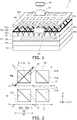
- FIG. 1 is a schematic perspective view of a semiconductor laser device according to a first embodiment.
- the semiconductor laser device 5 includes an active layer 25, a first layer 27, and a surface metal film 80. Multiple quantum well layers are stacked in the active layer 25; and the active layer 25 is configured to emit laser light of a terahertz wave by an intersubband transition.
- the terahertz wave is taken to be not less than 30 GHz and not more than 30 THz.
- the first layer 27 is provided on the active layer 25 and has a first surface 21a in which multiple pits 101 are provided to form a two-dimensional lattice.
- the surface metal film 80 is provided on the first layer 27; and multiple openings 80a are provided in the surface metal film 80.
- the openings 80a can be, for example, the gaps of a metal mesh, etc.
- each of the pits 101 is asymmetric with respect to a line parallel to a side of the lattice.
- laser light 60 passes through the multiple openings 80a and is emitted in a direction substantially perpendicular to the front surface of the active layer 25.
- the light intensity of laser light 61 emitted by passing through the openings 80a of the surface metal film 80 is measured by a detector 90 such as a bolometer, etc.
- the substantially perpendicular direction is not less than 81 degrees and not more than 99 degrees with respect to the front surface of the active layer 25.
- the semiconductor laser device 5 further includes a first electrode 50 provided between the first layer 27 and the surface metal film 80, electrically connected to the surface of the first layer 27, but insulated from the surface metal film 80.
- a first electrode 50 provided between the first layer 27 and the surface metal film 80, electrically connected to the surface of the first layer 27, but insulated from the surface metal film 80.
- the surface metal film 80 is illustrated as being separated from the surfaces of the first layer 27 and the first electrode 50 in FIG. 1 , actually, the surface metal film 80 is stacked with an insulating body or the like interposed.
- a stacked body 21 includes the first layer 27, the active layer 25, and a second layer.
- the multiple pits 101 that have opening ends at the first surface 21a of the stacked body 21 are provided in a two-dimensional lattice configuration and act as a periodic-structure PC (photonic crystal).
- the pits 101 have configurations in which triangular pyramid regions are cut out from the first surface 21a of the stacked body 21 toward the depth direction.
- the laser light 60 can have optical resonance along a QCL optical resonance direction 300 inside the active layer 25; and the mode is selected by the periodic-structure PC and further emitted from the first surface 21a along an optical axis substantially perpendicular to the first surface 21a due to a diffraction effect.
- the region lower than the first electrode 50 functions as a surface emitting portion.
- a voltage is supplied above and below the stacked body 21.
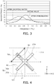
- FIG. 2 is a schematic plan view of the surface metal film of the semiconductor laser device according to the first embodiment.
- one opening 80a of the surface metal film 80 is provided for four pits 101.
- the laser light 60 is emitted from the surface emitting portion in an upward direction substantially perpendicular to the front surface of the active layer 25, passes through the openings 80a, and is emitted to the outside.
- the laser light 60 is a TM (Transverse Magnetic) wave polarized in the direction of the arrow.
- the crossing point of two orthogonal sides D and E in the XY plane is taken as a lattice point G; and the lattice spacing of the square lattice is taken as M.
- the lattice point G can be considered to be the centroid of the planar configuration of the pit 101, etc.
- Each of the pits 101 has non-line symmetry with respect to one side of the two sides D or E of the square lattice.
- the lattice may not be a square lattice and may be a lattice in which two sides are orthogonal.
- a portion of the terahertz wave can pass through the opening 80a.
- the transmittance of a terahertz wave of a wavelength of the width of the opening 80a or more can be set to 50% or more.
- the surface metal film 80 in which the openings 80a are provided acts as an external (LC) resonator for the terahertz wave.
- the resonant frequency of the external resonator changes. Therefore, the peak frequency of the transmission spectrum shifts.
- the first embodiment can emit a plane wave terahertz wave with high efficiency by using a metamaterial as the surface metal film 80.
- the transmission peak frequency can be shifted because the surface metal film 80 is used as an external resonator.
- the detection of fine particles, etc. can be performed by detecting the shift of the transmission peak frequency.
- the fine particle 90 including a microbe, bacteria such as coliform bacteria, or the like is adhered at the opening 80a vicinity of the surface metal film 80 of the opening 80a.
- the change of the transmittance due to the fine particles 90 is reduced by the amount of a region corresponding to the cross-sectional area of the fine particles 90 and is therefore small.
- the shift amount of the resonant frequency is large even if the amount of the fine particles 90 is low; therefore, the change of the transmittance is in a wide frequency range. Therefore, the existence or absence of the fine particles 90 can be detected with high accuracy.
- the fine particles 90 include PM 2.5, etc.
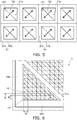
- FIG. 3 is a graph illustrating the transmittance for the frequency of the terahertz wave of the surface metal film of the semiconductor laser device according to the first embodiment.
- the vertical axis is the transmittance (%); and the horizontal axis is the frequency (THz) of the terahertz wave.
- the peak frequency decreased about 25 GHz with respect to the initial state.
- the peak frequency decreased about 300 GHz (the transmittance was about 33%).
- the absorption coefficient of water for the terahertz wave is high and is about 10 6 times the absorption coefficient for visible light or the like. Therefore, the shift amount of the resonant frequency after dropping the water onto the immobilized fine particle 90 becomes large; and the detection accuracy of the fine particle 90 increases.
- the shift amount of the resonant frequency is larger than the shift amount when the fine particle 90 exists.
- a single wavelength of the laser light 60 can be set within a range including the peak vicinity of the initial spectrum and the peak vicinity of the fine particle spectrum after dropping the water.
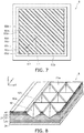
- FIG. 4 is a schematic plan view illustrating a modification of the surface metal film.
- the planar configuration of the opening 80a is a cross shape.
- the chip of the semiconductor laser device 5 should be replaced after the measurement. If the fine particle 90 is placed on a plate that is transparent to the terahertz wave, it is unnecessary to replace the chip.
- FIG. 5 is a schematic plan view illustrating another example of the arrangement of the openings of the surface metal film.
- the pitch of the openings may be equal to the pitch M of the two-dimensional diffraction grating. Or, it is unnecessary for the pitch of the openings to be an integer multiple of the pitch M of the two-dimensional diffraction grating. In other words, it is sufficient for the openings 80a to be arranged so that the resonant frequency is shifted.
- FIG. 6 is a schematic plan view of the surface emitting portion of the semiconductor laser device of the first embodiment.
- the pit 101 has a configuration in which a triangular pyramid, a truncated triangular pyramid, or the like is cut out downward from the first surface 21a of the stacked body 21.
- the configuration of the pit 101 is not limited thereto.
- the opening end of the pit 101 is illustrated by a right triangle.
- the two sides that sandwich the right angle are parallel respectively to the two sides of frame portions 50a and 50b; and the oblique side is parallel to a stripe portion 50c of the first electrode 50.
- the active layer 25 has a configuration in which a relaxation region is stacked alternately with an intersubband transition light emitting region made of a quantum well layer including a well layer and a barrier layer.
- the quantum well includes, for example, a well layer made of In 0.669 Ga 0.331 As doped with Si, and a barrier layer made of In 0.362 Al 0.638 As doped with Si. It is more favorable for the quantum well layer to have a multi-quantum well (MQW: Multi-Quantum Well) structure in which at least two well layers and multiple barrier layers are further stacked alternately.
- the relaxation region also can include a quantum well layer.
- a QCL has TM (Transverse Magnetic) polarized light of which the polarization direction is parallel to the front surface of the active layer 25; and for resonator mirrors sandwiching the active layer from the front surface and the back surface as in a p-n junction surface emitting laser, stimulated emission does not occur because the propagation directions of the light and the polarized light are aligned.
- TM Transverse Magnetic
- the QCL it is possible to resonate and amplify the stimulated emission light because the propagation direction of the stimulated emission light is a direction parallel to the front surface of the active layer 25. Further, in the case of a structure that is periodic and has anisotropy in the periodic structure, it is possible to extract the stimulated emission light in a direction substantially perpendicular to the front surface of the active layer 25. That is, a surface emitting laser is realizable in which the wavelength region is longer than the mid-infrared region which was previously realizable only by a QCL.
- the surface emitting laser it is unnecessary to form a resonator by cleaving as in an edge emitting laser; and the decrease of the yield due to the cleaving can be prevented. Further, in an edge emitting laser, the resonator is first formed by the cleaving; therefore, it is necessary to perform inspections after cleaving; and the cost of inspection is high compared to an LED or the like for which the inspections can be performed using an auto-prober or the like for the wafer as-is.
- the QCL according to the first embodiment can be evaluated by an auto-prober in the wafer state; a large effect of reducing the inspection cost and/or the cost from the perspective of yield can be expected; and mass production and price reduction are easy for QCLs which had previously been expensive.
- FIG. 7 is a schematic plan view of the first electrode of the surface emitting portion.
- the width is taken as L1; and the pitch in a direction orthogonal to the stripe portion 50c is taken as L2.
- the multiple pits 101 are disposed in the region sandwiched between the stripe portions 50c.
- FIG. 8 is a partial schematic perspective view of the pit portion.
- the stacked body 21 can further include a contact layer 28 on the first layer 27. Also, an insulator layer 40 of SiO 2 , etc., can be provided on the first surface 21a.
- the surface metal film 80 can be planarized by further providing an insulator layer of SiO 2 , etc., inside the pits.
- FIG. 9 is a graph illustrating the current injection uniformity dependence and the relative light extraction efficiency dependence with respect to the number of pits.
- the horizontal axis is the number of pits inside one period of the stripe portion 50c of the electrode; and the vertical axis is the uniformity of the current injection and the relative light extraction efficiency.
- the uniformity of the current injection is normalized to be 100 in the case where two pits are included inside one period along a direction orthogonal to the stripe portion 50c.
- the relative light extraction efficiency is normalized to be 100 in the case where fifty pits are included inside one period along the direction orthogonal to the stripe portion 50c.
- the optimal solution is determined from the relationship between the surface area of an opening 50d of the first electrode 50 and the efficiency of the current injection and the relationship of the effect of the periodic structure of the first electrode 50 on the diffraction effect of the light extraction.
- FIG. 10 is a schematic perspective view of a semiconductor laser device according to a second embodiment.
- the first electrode is not provided in the semiconductor laser device according to the second embodiment.
- the surface metal film 80 functions as the first electrode and supplies a voltage to the surface emitting portion.
- the first electrode is unnecessary in the second embodiment; therefore, the manufacturing processes can be simple; and a cost reduction is easy.
- the low cost is favorable in the case where the chip of the semiconductor laser device 5 is replaced.
- the surface metal film 80 and the surface of the surface emitting portion actually are closely adhered despite being illustrated as being separated in FIG. 10 .
- FIG. 11 is a configuration diagram of a laser device according to a comparative example.
- a semiconductor laser element 105 that is used as a light source is an edge emitting QCL emitting single-mode laser light.
- the edge emitting QCL emits the laser light from the ridge waveguide in a direction orthogonal to the end surface of the ridge waveguide. In such a case, the beam diverges; and the cross section of the beam has an elliptical configuration. Therefore, the diverging emitted light is caused to be parallel light by using a collimating lens 200, etc.
- the parallel light that is irradiated from the light source 105 is reflected by a reflection plate 180, subsequently is concentrated by a lens 202, and is incident on a detector 190 such as a bolometer, etc.; and the light intensity of the parallel light is detected.
- the reflection plate 180 can be a metal plate having openings. For a terahertz wave, such an optical configuration is large such that the planar configuration of the laser device is several tens of cmxseveral tens of cm or the like; and the adjustment of such an optical configuration is not easy.
- the terahertz wave is emitted from the surface emitting portion substantially perpendicular upward from the active layer 25. Therefore, a complex configuration and a large optical system are unnecessary; therefore, a small semiconductor laser device that can emit a plane terahertz wave with high efficiency is possible.
Landscapes
- Physics & Mathematics (AREA)
- General Physics & Mathematics (AREA)
- Condensed Matter Physics & Semiconductors (AREA)
- Electromagnetism (AREA)
- Optics & Photonics (AREA)
- Life Sciences & Earth Sciences (AREA)
- Health & Medical Sciences (AREA)
- Chemical & Material Sciences (AREA)
- Analytical Chemistry (AREA)
- Biochemistry (AREA)
- General Health & Medical Sciences (AREA)
- Immunology (AREA)
- Pathology (AREA)
- Semiconductor Lasers (AREA)
Abstract
Description
- This invention relates to a semiconductor laser device.
- When using a quantum cascade laser as a light source of a terahertz wave, a laser oscillation of 30 GHz to 30 THz is possible due to an intersubband transition of electrons.
- In the case where an edge emitting quantum cascade laser is used as the light source, a collimator lens is necessary to cause the spreading laser light emitted from the end surface to be parallel light; and the exterior form of the laser device becomes large.
- [Patent Document 1]
JP 2009-231773 - A semiconductor laser device is provided that is capable of emitting a terahertz wave of a plane wave with high efficiency.
- A semiconductor laser device of an embodiment includes an active layer, a first layer, and a surface metal film. Multiple quantum well layers are stacked in the active layer; and the active layer is configured to emit laser light of a terahertz wave by an intersubband transition. The first layer is provided on the active layer and has a first surface in which multiple pits are provided to form a two-dimensional lattice. The surface metal film is provided on the first layer and has multiple openings. Each of the pits is asymmetric with respect to a line parallel to a side of the lattice. The laser light passes through the multiple openings and is emitted in a direction substantially perpendicular to the active layer.
-
- [
FIG. 1 ]
FIG. 1 is a schematic perspective view of a semiconductor laser device according to a first embodiment. - [
FIG. 2 ]
FIG. 2 is a schematic plan view of the surface metal film of the semiconductor laser device according to the first embodiment. - [
FIG. 3 ]
FIG. 3 is a graph illustrating the transmittance for the frequency of the terahertz wave of the surface metal film of the semiconductor laser device according to the first embodiment. - [
FIG. 4 ]
FIG. 4 is a schematic plan view illustrating a modification of the surface metal film. - [
FIG. 5 ]
FIG. 5 is a schematic plan view illustrating another example of the arrangement of the openings of the surface metal film. - [
FIG. 6 ]
FIG. 6 is a schematic plan view of the surface emitting portion of the semiconductor laser device of the first embodiment. - [
FIG. 7 ]
FIG. 7 is a schematic plan view of the first electrode of the surface emitting portion. - [
FIG. 8 ]
FIG. 8 is a partial schematic perspective view of the pit portion. - [
FIG. 9 ]
FIG. 9 is a graph illustrating the current injection uniformity dependence and the relative light extraction efficiency dependence with respect to the number of pits. - [
FIG. 10 ]
FIG. 10 is a schematic perspective view of a semiconductor laser device according to a second embodiment. - [
FIG. 11 ]
FIG. 11 is a configuration diagram of a laser device according to a comparative example. - Embodiments of the invention will now be described with reference to the drawings.
-
FIG. 1 is a schematic perspective view of a semiconductor laser device according to a first embodiment. - The
semiconductor laser device 5 includes anactive layer 25, afirst layer 27, and asurface metal film 80. Multiple quantum well layers are stacked in theactive layer 25; and theactive layer 25 is configured to emit laser light of a terahertz wave by an intersubband transition. In the specification, the terahertz wave is taken to be not less than 30 GHz and not more than 30 THz. - The
first layer 27 is provided on theactive layer 25 and has afirst surface 21a in whichmultiple pits 101 are provided to form a two-dimensional lattice. Thesurface metal film 80 is provided on thefirst layer 27; andmultiple openings 80a are provided in thesurface metal film 80. Theopenings 80a can be, for example, the gaps of a metal mesh, etc. - The planar configuration of each of the
pits 101 is asymmetric with respect to a line parallel to a side of the lattice. Also,laser light 60 passes through themultiple openings 80a and is emitted in a direction substantially perpendicular to the front surface of theactive layer 25. The light intensity oflaser light 61 emitted by passing through theopenings 80a of thesurface metal film 80 is measured by adetector 90 such as a bolometer, etc. In the specification, the substantially perpendicular direction is not less than 81 degrees and not more than 99 degrees with respect to the front surface of theactive layer 25. - In the embodiment, the
semiconductor laser device 5 further includes afirst electrode 50 provided between thefirst layer 27 and thesurface metal film 80, electrically connected to the surface of thefirst layer 27, but insulated from thesurface metal film 80. Although thesurface metal film 80 is illustrated as being separated from the surfaces of thefirst layer 27 and thefirst electrode 50 inFIG. 1 , actually, thesurface metal film 80 is stacked with an insulating body or the like interposed. - A
stacked body 21 includes thefirst layer 27, theactive layer 25, and a second layer. Themultiple pits 101 that have opening ends at thefirst surface 21a of thestacked body 21 are provided in a two-dimensional lattice configuration and act as a periodic-structure PC (photonic crystal). For example, thepits 101 have configurations in which triangular pyramid regions are cut out from thefirst surface 21a of thestacked body 21 toward the depth direction. - The
laser light 60 can have optical resonance along a QCLoptical resonance direction 300 inside theactive layer 25; and the mode is selected by the periodic-structure PC and further emitted from thefirst surface 21a along an optical axis substantially perpendicular to thefirst surface 21a due to a diffraction effect. In other words, the region lower than thefirst electrode 50 functions as a surface emitting portion. A voltage is supplied above and below the stackedbody 21. -
FIG. 2 is a schematic plan view of the surface metal film of the semiconductor laser device according to the first embodiment. - In the drawing, one opening 80a of the
surface metal film 80 is provided for fourpits 101. Thelaser light 60 is emitted from the surface emitting portion in an upward direction substantially perpendicular to the front surface of theactive layer 25, passes through theopenings 80a, and is emitted to the outside. Thelaser light 60 is a TM (Transverse Magnetic) wave polarized in the direction of the arrow. - For the square lattice that forms the periodic-structure PC, the crossing point of two orthogonal sides D and E in the XY plane is taken as a lattice point G; and the lattice spacing of the square lattice is taken as M. For example, the lattice point G can be considered to be the centroid of the planar configuration of the
pit 101, etc. Each of thepits 101 has non-line symmetry with respect to one side of the two sides D or E of the square lattice. The lattice may not be a square lattice and may be a lattice in which two sides are orthogonal. - A portion of the terahertz wave can pass through the
opening 80a. For example, by changing the configuration and/or the size of theopening 80a, the transmittance of a terahertz wave of a wavelength of the width of theopening 80a or more can be set to 50% or more. Also, thesurface metal film 80 in which theopenings 80a are provided acts as an external (LC) resonator for the terahertz wave. In the case where afine particle 90 including a dielectric adheres at theopening 80a vicinity of thesurface metal film 80, the resonant frequency of the external resonator changes. Therefore, the peak frequency of the transmission spectrum shifts. In other words, the first embodiment can emit a plane wave terahertz wave with high efficiency by using a metamaterial as thesurface metal film 80. - Also, in the
semiconductor laser device 5 of the first embodiment, the transmission peak frequency can be shifted because thesurface metal film 80 is used as an external resonator. The detection of fine particles, etc., can be performed by detecting the shift of the transmission peak frequency. For example, it is taken that thefine particle 90 including a microbe, bacteria such as coliform bacteria, or the like is adhered at theopening 80a vicinity of thesurface metal film 80 of theopening 80a. - In the case where the wavelength of the laser light is near visible light, the change of the transmittance due to the
fine particles 90 is reduced by the amount of a region corresponding to the cross-sectional area of thefine particles 90 and is therefore small. Conversely, in the case where the wavelength of the laser light is near a terahertz wave, the shift amount of the resonant frequency is large even if the amount of thefine particles 90 is low; therefore, the change of the transmittance is in a wide frequency range. Therefore, the existence or absence of thefine particles 90 can be detected with high accuracy. Thefine particles 90 include PM 2.5, etc. -
FIG. 3 is a graph illustrating the transmittance for the frequency of the terahertz wave of the surface metal film of the semiconductor laser device according to the first embodiment. - The vertical axis is the transmittance (%); and the horizontal axis is the frequency (THz) of the terahertz wave. After immobilizing coliform bacteria, water was dropped; and the transmission spectrum was measured. The initial state is illustrated by the broken line; the state after the coliform bacteria immobilization is illustrated by the dotted line; and the state after the dropping of the water is illustrated by the solid line. The transmission spectrum intensity is measurable using a spectrometer, etc.
- By immobilizing the coliform bacteria, the peak frequency decreased about 25 GHz with respect to the initial state. By dropping the water, the peak frequency decreased about 300 GHz (the transmittance was about 33%). The absorption coefficient of water for the terahertz wave is high and is about 106 times the absorption coefficient for visible light or the like. Therefore, the shift amount of the resonant frequency after dropping the water onto the immobilized
fine particle 90 becomes large; and the detection accuracy of thefine particle 90 increases. - In the case of only water not including the
fine particle 90, the shift amount of the resonant frequency is larger than the shift amount when thefine particle 90 exists. For example, a single wavelength of thelaser light 60 can be set within a range including the peak vicinity of the initial spectrum and the peak vicinity of the fine particle spectrum after dropping the water. -
FIG. 4 is a schematic plan view illustrating a modification of the surface metal film. - In the modification of
FIG. 4 , the planar configuration of theopening 80a is a cross shape. In the case where thefine particle 90 is placed directly on thesurface metal film 80, the chip of thesemiconductor laser device 5 should be replaced after the measurement. If thefine particle 90 is placed on a plate that is transparent to the terahertz wave, it is unnecessary to replace the chip. -
FIG. 5 is a schematic plan view illustrating another example of the arrangement of the openings of the surface metal film. - The pitch of the openings may be equal to the pitch M of the two-dimensional diffraction grating. Or, it is unnecessary for the pitch of the openings to be an integer multiple of the pitch M of the two-dimensional diffraction grating. In other words, it is sufficient for the
openings 80a to be arranged so that the resonant frequency is shifted. -
FIG. 6 is a schematic plan view of the surface emitting portion of the semiconductor laser device of the first embodiment. - The
pit 101 has a configuration in which a triangular pyramid, a truncated triangular pyramid, or the like is cut out downward from thefirst surface 21a of the stackedbody 21. The configuration of thepit 101 is not limited thereto. In the drawing, the opening end of thepit 101 is illustrated by a right triangle. The two sides that sandwich the right angle are parallel respectively to the two sides offrame portions stripe portion 50c of thefirst electrode 50. - The
active layer 25 has a configuration in which a relaxation region is stacked alternately with an intersubband transition light emitting region made of a quantum well layer including a well layer and a barrier layer. The quantum well includes, for example, a well layer made of In0.669Ga0.331As doped with Si, and a barrier layer made of In0.362Al0.638As doped with Si. It is more favorable for the quantum well layer to have a multi-quantum well (MQW: Multi-Quantum Well) structure in which at least two well layers and multiple barrier layers are further stacked alternately. Also, the relaxation region also can include a quantum well layer. - A QCL has TM (Transverse Magnetic) polarized light of which the polarization direction is parallel to the front surface of the
active layer 25; and for resonator mirrors sandwiching the active layer from the front surface and the back surface as in a p-n junction surface emitting laser, stimulated emission does not occur because the propagation directions of the light and the polarized light are aligned. In other words, it was impossible to realize a VCSEL (Veryical Cavity Surface Emitting Laser: surface emitting laser). - Conversely, in the QCL according to the first embodiment, it is possible to resonate and amplify the stimulated emission light because the propagation direction of the stimulated emission light is a direction parallel to the front surface of the
active layer 25. Further, in the case of a structure that is periodic and has anisotropy in the periodic structure, it is possible to extract the stimulated emission light in a direction substantially perpendicular to the front surface of theactive layer 25. That is, a surface emitting laser is realizable in which the wavelength region is longer than the mid-infrared region which was previously realizable only by a QCL. - In the surface emitting laser, it is unnecessary to form a resonator by cleaving as in an edge emitting laser; and the decrease of the yield due to the cleaving can be prevented. Further, in an edge emitting laser, the resonator is first formed by the cleaving; therefore, it is necessary to perform inspections after cleaving; and the cost of inspection is high compared to an LED or the like for which the inspections can be performed using an auto-prober or the like for the wafer as-is.
- Conversely, the QCL according to the first embodiment can be evaluated by an auto-prober in the wafer state; a large effect of reducing the inspection cost and/or the cost from the perspective of yield can be expected; and mass production and price reduction are easy for QCLs which had previously been expensive.
-
FIG. 7 is a schematic plan view of the first electrode of the surface emitting portion. - For the
stripe portion 50c, the width is taken as L1; and the pitch in a direction orthogonal to thestripe portion 50c is taken as L2. Themultiple pits 101 are disposed in the region sandwiched between thestripe portions 50c. -
FIG. 8 is a partial schematic perspective view of the pit portion. - The
stacked body 21 can further include acontact layer 28 on thefirst layer 27. Also, aninsulator layer 40 of SiO2, etc., can be provided on thefirst surface 21a. Thesurface metal film 80 can be planarized by further providing an insulator layer of SiO2, etc., inside the pits. -
FIG. 9 is a graph illustrating the current injection uniformity dependence and the relative light extraction efficiency dependence with respect to the number of pits. - The horizontal axis is the number of pits inside one period of the
stripe portion 50c of the electrode; and the vertical axis is the uniformity of the current injection and the relative light extraction efficiency. In the case where thestripe portion 50c of thefirst electrode 50 has a one-dimensional periodic structure, the uniformity of the current injection is normalized to be 100 in the case where two pits are included inside one period along a direction orthogonal to thestripe portion 50c. - Also, in the case where the
stripe portion 50c of thefirst electrode 50 has a one-dimensional periodic structure, the relative light extraction efficiency is normalized to be 100 in the case where fifty pits are included inside one period along the direction orthogonal to thestripe portion 50c. - As the number of the
pits 101 inside one period along the direction orthogonal to thestripe portion 50c increases, the uniformity of the current injection decreases; but the relative light extraction efficiency increases. In other words, by setting the number of thepits 101 inside one period to be not less than 5 and not more than 20, both the uniformity of the current injection and the laser light extraction efficiency can be realized. Thus, the optimal solution is determined from the relationship between the surface area of anopening 50d of thefirst electrode 50 and the efficiency of the current injection and the relationship of the effect of the periodic structure of thefirst electrode 50 on the diffraction effect of the light extraction. -
FIG. 10 is a schematic perspective view of a semiconductor laser device according to a second embodiment. - The first electrode is not provided in the semiconductor laser device according to the second embodiment. In other words, the
surface metal film 80 functions as the first electrode and supplies a voltage to the surface emitting portion. The first electrode is unnecessary in the second embodiment; therefore, the manufacturing processes can be simple; and a cost reduction is easy. The low cost is favorable in the case where the chip of thesemiconductor laser device 5 is replaced. Thesurface metal film 80 and the surface of the surface emitting portion (the surface of the first layer 27) actually are closely adhered despite being illustrated as being separated inFIG. 10 . -
FIG. 11 is a configuration diagram of a laser device according to a comparative example. - A
semiconductor laser element 105 that is used as a light source is an edge emitting QCL emitting single-mode laser light. The edge emitting QCL emits the laser light from the ridge waveguide in a direction orthogonal to the end surface of the ridge waveguide. In such a case, the beam diverges; and the cross section of the beam has an elliptical configuration. Therefore, the diverging emitted light is caused to be parallel light by using acollimating lens 200, etc. - The parallel light that is irradiated from the
light source 105 is reflected by areflection plate 180, subsequently is concentrated by alens 202, and is incident on adetector 190 such as a bolometer, etc.; and the light intensity of the parallel light is detected. Thereflection plate 180 can be a metal plate having openings. For a terahertz wave, such an optical configuration is large such that the planar configuration of the laser device is several tens of cmxseveral tens of cm or the like; and the adjustment of such an optical configuration is not easy. - Conversely, according to the semiconductor laser device of the embodiment, the terahertz wave is emitted from the surface emitting portion substantially perpendicular upward from the
active layer 25. Therefore, a complex configuration and a large optical system are unnecessary; therefore, a small semiconductor laser device that can emit a plane terahertz wave with high efficiency is possible. - While certain embodiments have been described, these embodiments have been presented by way of example only, and are not intended to limit the scope of the inventions. Indeed, the novel embodiments described herein may be embodied in a variety of other forms; furthermore, various omissions, substitutions and changes in the form of the embodiments described herein may be made without departing from the spirit of the inventions. The accompanying claims and their equivalents are intended to cover such forms or modifications as would fall within the scope and spirit of the invention.
Claims (9)
- A semiconductor laser device, comprising:an active layer configured to emit laser light of a terahertz wave by an intersubband transition, a plurality of quantum well layers being stacked in the active layer;a first layer having a first surface and being provided on the active layer, a plurality of pits being provided in the first surface to form a two-dimensional lattice; anda surface metal film provided on the first layer, a plurality of openings being provided in the surface metal film,each of the pits being asymmetric with respect to a line parallel to a side of the lattice, andthe laser light passing through the plurality of openings and being emitted in a direction substantially perpendicular to the active layer.
- The semiconductor laser device according to claim 1, wherein the lattice of the first layer includes the pits having configurations of prescribed regions of the first layer cut out from the first surface toward a depth direction.
- The semiconductor laser device according to claim 1, wherein the openings form a two-dimensional lattice.
- The semiconductor laser device according to claim 2, wherein the openings form a two-dimensional lattice.
- The semiconductor laser device according to claim 3, wherein a pitch of the lattice of the openings is different from a pitch of the lattice of the first layer.
- The semiconductor laser device according to claim 4, wherein a pitch of the lattice of the openings is different from a pitch of the lattice of the first layer.
- The semiconductor laser device according to any one of claims 1 to 6, further comprising a first electrode provided between the first layer and the surface metal film, electrically connected to a surface of the first layer, but insulated from the surface metal film.
- The semiconductor laser device according to claim 7, wherein
the first electrode includes a frame portion and a plurality of stripe portions, two end portions of each stripe portion being linked to the frame portion, and
the plurality of stripe portions obliquely crosses the frame portion and is arranged to be mutually parallel at a prescribed pitch. - The semiconductor laser device according to claim 8, wherein an opening of the first electrode is asymmetric with respect to a line parallel to a side of the lattice of the first layer.
Applications Claiming Priority (2)
| Application Number | Priority Date | Filing Date | Title |
|---|---|---|---|
| JP2016051671A JP6808336B2 (en) | 2016-03-15 | 2016-03-15 | Semiconductor laser device |
| PCT/JP2016/075859 WO2017158876A1 (en) | 2016-03-15 | 2016-09-02 | Semiconductor laser device |
Publications (3)
| Publication Number | Publication Date |
|---|---|
| EP3432428A1 true EP3432428A1 (en) | 2019-01-23 |
| EP3432428A4 EP3432428A4 (en) | 2019-12-04 |
| EP3432428B1 EP3432428B1 (en) | 2021-10-20 |
Family
ID=59851381
Family Applications (1)
| Application Number | Title | Priority Date | Filing Date |
|---|---|---|---|
| EP16894493.2A Active EP3432428B1 (en) | 2016-03-15 | 2016-09-02 | Semiconductor laser device |
Country Status (5)
| Country | Link |
|---|---|
| US (1) | US20190081456A1 (en) |
| EP (1) | EP3432428B1 (en) |
| JP (1) | JP6808336B2 (en) |
| CN (1) | CN108701964B (en) |
| WO (1) | WO2017158876A1 (en) |
Families Citing this family (2)
| Publication number | Priority date | Publication date | Assignee | Title |
|---|---|---|---|---|
| CN110718763B (en) * | 2019-09-17 | 2020-08-04 | 北京航空航天大学 | A tunable metamaterial device based on CMOS technology |
| TWI844803B (en) * | 2021-10-28 | 2024-06-11 | 鴻海精密工業股份有限公司 | Photonic crystal surface-emitting laser device and optical system |
Family Cites Families (27)
| Publication number | Priority date | Publication date | Assignee | Title |
|---|---|---|---|---|
| US6400744B1 (en) * | 2000-02-25 | 2002-06-04 | Lucent Technologies, Inc. | Apparatus comprising a quantum cascade laser having improved distributed feedback for single-mode operation |
| US6826223B1 (en) * | 2003-05-28 | 2004-11-30 | The United States Of America As Represented By The Secretary Of The Navy | Surface-emitting photonic crystal distributed feedback laser systems and methods |
| US7535946B2 (en) * | 2006-11-16 | 2009-05-19 | Canon Kabushiki Kaisha | Structure using photonic crystal and surface emitting laser |
| JP4906704B2 (en) * | 2007-02-08 | 2012-03-28 | キヤノン株式会社 | Surface emitting laser and light emitting device provided with surface emitting laser |
| US20080197369A1 (en) * | 2007-02-20 | 2008-08-21 | Cree, Inc. | Double flip semiconductor device and method for fabrication |
| US7545841B2 (en) * | 2007-04-24 | 2009-06-09 | Hewlett-Packard Development Company, L.P. | Composite material with proximal gain medium |
| JP4719198B2 (en) * | 2007-09-12 | 2011-07-06 | 日本電信電話株式会社 | Semiconductor laser module and laser light source |
| JP5216384B2 (en) * | 2008-03-19 | 2013-06-19 | 株式会社東芝 | Light emitting device |
| WO2010044193A1 (en) * | 2008-10-14 | 2010-04-22 | 国立大学法人東北大学 | Sample analysis method |
| US8285091B2 (en) * | 2009-07-10 | 2012-10-09 | Massachusetts Institute Of Technology | Efficient terahertz sources based on difference-frequency generation in triply-resonant photonic resonators |
| JP5709178B2 (en) * | 2010-03-01 | 2015-04-30 | 国立大学法人京都大学 | Photonic crystal laser |
| CN101895057A (en) * | 2010-05-24 | 2010-11-24 | 中国科学院长春光学精密机械与物理研究所 | An inter-injection-locked two-dimensional surface-emitting laser array |
| US8805147B2 (en) * | 2011-05-17 | 2014-08-12 | Canon Kabushiki Kaisha | Waveguide, apparatus including the waveguide, and method of manufacturing the waveguide |
| JP5771818B2 (en) * | 2011-06-13 | 2015-09-02 | 国立研究開発法人理化学研究所 | Unit resonator for metamaterial, resonator array, and method for manufacturing metamaterial |
| GB201117480D0 (en) * | 2011-10-10 | 2011-11-23 | Palikaras George | Filter |
| CN202394003U (en) * | 2011-12-19 | 2012-08-22 | 东南大学 | TeraHertz high-speed modulator |
| CN102570307A (en) * | 2012-02-02 | 2012-07-11 | 中国科学院上海微系统与信息技术研究所 | Single-mode large-power THz quantum cascade laser (QCL) and manufacturing technology thereof |
| JP2013165152A (en) * | 2012-02-10 | 2013-08-22 | Nippon Telegr & Teleph Corp <Ntt> | Plasmon thin film laser |
| US9088133B2 (en) * | 2012-02-28 | 2015-07-21 | Kyoto University | Two-dimensional photonic crystal surface emitting laser |
| JP2013222810A (en) * | 2012-04-16 | 2013-10-28 | Hamamatsu Photonics Kk | Semiconductor laser device |
| JP2014027264A (en) * | 2012-06-22 | 2014-02-06 | Canon Inc | Surface emitting laser |
| US8831058B2 (en) * | 2012-09-06 | 2014-09-09 | Bae Systems Information And Electronic Systems Integration Inc. | Hyperbolic metamaterials as distributed bragg mirrors for high power VCSEL devices |
| JP6213915B2 (en) * | 2013-03-04 | 2017-10-18 | 国立大学法人京都大学 | Semiconductor laser element |
| JP6080941B2 (en) * | 2013-03-08 | 2017-02-15 | 国立研究開発法人科学技術振興機構 | Two-dimensional photonic crystal surface emitting laser |
| WO2015104555A2 (en) * | 2014-01-10 | 2015-07-16 | King's College London | Device and method |
| JP6182230B1 (en) * | 2016-03-15 | 2017-08-16 | 株式会社東芝 | Surface emitting quantum cascade laser |
| JP2017168591A (en) * | 2016-03-15 | 2017-09-21 | 株式会社東芝 | Semiconductor laser device |
-
2016
- 2016-03-15 JP JP2016051671A patent/JP6808336B2/en active Active
- 2016-09-02 EP EP16894493.2A patent/EP3432428B1/en active Active
- 2016-09-02 WO PCT/JP2016/075859 patent/WO2017158876A1/en not_active Ceased
- 2016-09-02 US US16/084,490 patent/US20190081456A1/en not_active Abandoned
- 2016-09-02 CN CN201680083246.7A patent/CN108701964B/en active Active
Also Published As
| Publication number | Publication date |
|---|---|
| JP2017168595A (en) | 2017-09-21 |
| WO2017158876A1 (en) | 2017-09-21 |
| US20190081456A1 (en) | 2019-03-14 |
| EP3432428B1 (en) | 2021-10-20 |
| CN108701964A (en) | 2018-10-23 |
| CN108701964B (en) | 2020-10-27 |
| EP3432428A4 (en) | 2019-12-04 |
| JP6808336B2 (en) | 2021-01-06 |
Similar Documents
| Publication | Publication Date | Title |
|---|---|---|
| EP3220495B1 (en) | Surface emitting quantum cascade laser | |
| US10069036B2 (en) | Resonant optical cavity light emitting device | |
| US8328396B2 (en) | Methods and apparatus for improving collimation of radiation beams | |
| EP3457506A1 (en) | Surface emitting quantum cascade laser | |
| US20060044212A1 (en) | Composite material with powered resonant cells | |
| US20130266034A1 (en) | Methods and apparatuses for engineering electromagnetic radiation | |
| US20090074026A1 (en) | Structure having photonic crystal and surface-emitting laser | |
| CN101258652B (en) | Two-dimensional photonic crystal surface emitting laser light source | |
| EP1610427A1 (en) | Two-dimensional photonic crystal surface-emitting laser | |
| US20190013435A1 (en) | Resonant optical cavity light emitting device | |
| US20070075318A1 (en) | Two-dimensional photonic crystal surface-emitting laser | |
| CN101421889A (en) | Vcsel with photonic crystal mirror for waveguiding by diffraction | |
| WO2005086302A1 (en) | Two-dimensional photonic crystal surface-emitting laser light source | |
| JP5138898B2 (en) | Two-dimensional photonic crystal surface emitting laser light source | |
| KR102100931B1 (en) | Photoconductive antenna | |
| US20130003768A1 (en) | Photonic crystal laser | |
| EP3432428B1 (en) | Semiconductor laser device | |
| JP2015135414A (en) | Terahertz band wavelength plate and terahertz wave measurement device | |
| JP2014053346A (en) | Short optical pulse generator, terahertz wave generator, camera, imaging device, and measuring device | |
| JP2017188700A (en) | Surface emitting quantum cascade laser | |
| Yu et al. | Wavefront engineering for mid-infrared and terahertz quantum cascade lasers | |
| JP6774400B2 (en) | Surface emission quantum cascade laser | |
| WO2020100611A1 (en) | Nanowire optical device | |
| US20230163566A1 (en) | Two-dimensional photonic-crystal laser | |
| WO2015080666A1 (en) | Light source including a nanoparticle |
Legal Events
| Date | Code | Title | Description |
|---|---|---|---|
| STAA | Information on the status of an ep patent application or granted ep patent |
Free format text: STATUS: THE INTERNATIONAL PUBLICATION HAS BEEN MADE |
|
| PUAI | Public reference made under article 153(3) epc to a published international application that has entered the european phase |
Free format text: ORIGINAL CODE: 0009012 |
|
| STAA | Information on the status of an ep patent application or granted ep patent |
Free format text: STATUS: REQUEST FOR EXAMINATION WAS MADE |
|
| 17P | Request for examination filed |
Effective date: 20180913 |
|
| AK | Designated contracting states |
Kind code of ref document: A1 Designated state(s): AL AT BE BG CH CY CZ DE DK EE ES FI FR GB GR HR HU IE IS IT LI LT LU LV MC MK MT NL NO PL PT RO RS SE SI SK SM TR |
|
| AX | Request for extension of the european patent |
Extension state: BA ME |
|
| DAV | Request for validation of the european patent (deleted) | ||
| DAX | Request for extension of the european patent (deleted) | ||
| A4 | Supplementary search report drawn up and despatched |
Effective date: 20191104 |
|
| RIC1 | Information provided on ipc code assigned before grant |
Ipc: H01S 5/22 20060101ALN20191028BHEP Ipc: H01S 5/14 20060101ALN20191028BHEP Ipc: H01S 5/20 20060101ALN20191028BHEP Ipc: H01S 5/34 20060101ALI20191028BHEP Ipc: H01S 5/18 20060101ALI20191028BHEP Ipc: H01S 5/042 20060101AFI20191028BHEP Ipc: H01S 5/10 20060101ALI20191028BHEP |
|
| STAA | Information on the status of an ep patent application or granted ep patent |
Free format text: STATUS: EXAMINATION IS IN PROGRESS |
|
| 17Q | First examination report despatched |
Effective date: 20200525 |
|
| RIC1 | Information provided on ipc code assigned before grant |
Ipc: H01S 5/14 20060101ALN20200515BHEP Ipc: H01S 5/20 20060101ALN20200515BHEP Ipc: H01S 5/34 20060101ALI20200515BHEP Ipc: H01S 5/042 20060101AFI20200515BHEP Ipc: H01S 5/10 20060101ALI20200515BHEP Ipc: H01S 5/18 20060101ALI20200515BHEP Ipc: H01S 5/22 20060101ALN20200515BHEP |
|
| REG | Reference to a national code |
Ref country code: DE Ref legal event code: R079 Ref document number: 602016065288 Country of ref document: DE Free format text: PREVIOUS MAIN CLASS: H01S0005180000 Ipc: H01S0005042000 |
|
| RIC1 | Information provided on ipc code assigned before grant |
Ipc: H01S 5/14 20060101ALN20210629BHEP Ipc: H01S 5/22 20060101ALN20210629BHEP Ipc: H01S 5/20 20060101ALN20210629BHEP Ipc: H01S 5/11 20210101ALI20210629BHEP Ipc: H01S 5/34 20060101ALI20210629BHEP Ipc: H01S 5/18 20210101ALI20210629BHEP Ipc: H01S 5/10 20210101ALI20210629BHEP Ipc: H01S 5/042 20060101AFI20210629BHEP |
|
| GRAP | Despatch of communication of intention to grant a patent |
Free format text: ORIGINAL CODE: EPIDOSNIGR1 |
|
| STAA | Information on the status of an ep patent application or granted ep patent |
Free format text: STATUS: GRANT OF PATENT IS INTENDED |
|
| RIC1 | Information provided on ipc code assigned before grant |
Ipc: H01S 5/14 20060101ALN20210716BHEP Ipc: H01S 5/22 20060101ALN20210716BHEP Ipc: H01S 5/20 20060101ALN20210716BHEP Ipc: H01S 5/11 20210101ALI20210716BHEP Ipc: H01S 5/34 20060101ALI20210716BHEP Ipc: H01S 5/18 20210101ALI20210716BHEP Ipc: H01S 5/10 20210101ALI20210716BHEP Ipc: H01S 5/042 20060101AFI20210716BHEP |
|
| RIC1 | Information provided on ipc code assigned before grant |
Ipc: H01S 5/14 20060101ALN20210726BHEP Ipc: H01S 5/22 20060101ALN20210726BHEP Ipc: H01S 5/20 20060101ALN20210726BHEP Ipc: H01S 5/11 20210101ALI20210726BHEP Ipc: H01S 5/34 20060101ALI20210726BHEP Ipc: H01S 5/18 20210101ALI20210726BHEP Ipc: H01S 5/10 20210101ALI20210726BHEP Ipc: H01S 5/042 20060101AFI20210726BHEP |
|
| GRAS | Grant fee paid |
Free format text: ORIGINAL CODE: EPIDOSNIGR3 |
|
| INTG | Intention to grant announced |
Effective date: 20210818 |
|
| GRAA | (expected) grant |
Free format text: ORIGINAL CODE: 0009210 |
|
| STAA | Information on the status of an ep patent application or granted ep patent |
Free format text: STATUS: THE PATENT HAS BEEN GRANTED |
|
| AK | Designated contracting states |
Kind code of ref document: B1 Designated state(s): AL AT BE BG CH CY CZ DE DK EE ES FI FR GB GR HR HU IE IS IT LI LT LU LV MC MK MT NL NO PL PT RO RS SE SI SK SM TR |
|
| REG | Reference to a national code |
Ref country code: GB Ref legal event code: FG4D |
|
| REG | Reference to a national code |
Ref country code: CH Ref legal event code: EP |
|
| REG | Reference to a national code |
Ref country code: IE Ref legal event code: FG4D |
|
| REG | Reference to a national code |
Ref country code: DE Ref legal event code: R096 Ref document number: 602016065288 Country of ref document: DE |
|
| REG | Reference to a national code |
Ref country code: AT Ref legal event code: REF Ref document number: 1440704 Country of ref document: AT Kind code of ref document: T Effective date: 20211115 |
|
| REG | Reference to a national code |
Ref country code: LT Ref legal event code: MG9D |
|
| REG | Reference to a national code |
Ref country code: NL Ref legal event code: MP Effective date: 20211020 |
|
| REG | Reference to a national code |
Ref country code: AT Ref legal event code: MK05 Ref document number: 1440704 Country of ref document: AT Kind code of ref document: T Effective date: 20211020 |
|
| PG25 | Lapsed in a contracting state [announced via postgrant information from national office to epo] |
Ref country code: RS Free format text: LAPSE BECAUSE OF FAILURE TO SUBMIT A TRANSLATION OF THE DESCRIPTION OR TO PAY THE FEE WITHIN THE PRESCRIBED TIME-LIMIT Effective date: 20211020 Ref country code: LT Free format text: LAPSE BECAUSE OF FAILURE TO SUBMIT A TRANSLATION OF THE DESCRIPTION OR TO PAY THE FEE WITHIN THE PRESCRIBED TIME-LIMIT Effective date: 20211020 Ref country code: FI Free format text: LAPSE BECAUSE OF FAILURE TO SUBMIT A TRANSLATION OF THE DESCRIPTION OR TO PAY THE FEE WITHIN THE PRESCRIBED TIME-LIMIT Effective date: 20211020 Ref country code: BG Free format text: LAPSE BECAUSE OF FAILURE TO SUBMIT A TRANSLATION OF THE DESCRIPTION OR TO PAY THE FEE WITHIN THE PRESCRIBED TIME-LIMIT Effective date: 20220120 Ref country code: AT Free format text: LAPSE BECAUSE OF FAILURE TO SUBMIT A TRANSLATION OF THE DESCRIPTION OR TO PAY THE FEE WITHIN THE PRESCRIBED TIME-LIMIT Effective date: 20211020 |
|
| PG25 | Lapsed in a contracting state [announced via postgrant information from national office to epo] |
Ref country code: IS Free format text: LAPSE BECAUSE OF FAILURE TO SUBMIT A TRANSLATION OF THE DESCRIPTION OR TO PAY THE FEE WITHIN THE PRESCRIBED TIME-LIMIT Effective date: 20220220 Ref country code: SE Free format text: LAPSE BECAUSE OF FAILURE TO SUBMIT A TRANSLATION OF THE DESCRIPTION OR TO PAY THE FEE WITHIN THE PRESCRIBED TIME-LIMIT Effective date: 20211020 Ref country code: PT Free format text: LAPSE BECAUSE OF FAILURE TO SUBMIT A TRANSLATION OF THE DESCRIPTION OR TO PAY THE FEE WITHIN THE PRESCRIBED TIME-LIMIT Effective date: 20220221 Ref country code: PL Free format text: LAPSE BECAUSE OF FAILURE TO SUBMIT A TRANSLATION OF THE DESCRIPTION OR TO PAY THE FEE WITHIN THE PRESCRIBED TIME-LIMIT Effective date: 20211020 Ref country code: NO Free format text: LAPSE BECAUSE OF FAILURE TO SUBMIT A TRANSLATION OF THE DESCRIPTION OR TO PAY THE FEE WITHIN THE PRESCRIBED TIME-LIMIT Effective date: 20220120 Ref country code: NL Free format text: LAPSE BECAUSE OF FAILURE TO SUBMIT A TRANSLATION OF THE DESCRIPTION OR TO PAY THE FEE WITHIN THE PRESCRIBED TIME-LIMIT Effective date: 20211020 Ref country code: LV Free format text: LAPSE BECAUSE OF FAILURE TO SUBMIT A TRANSLATION OF THE DESCRIPTION OR TO PAY THE FEE WITHIN THE PRESCRIBED TIME-LIMIT Effective date: 20211020 Ref country code: HR Free format text: LAPSE BECAUSE OF FAILURE TO SUBMIT A TRANSLATION OF THE DESCRIPTION OR TO PAY THE FEE WITHIN THE PRESCRIBED TIME-LIMIT Effective date: 20211020 Ref country code: GR Free format text: LAPSE BECAUSE OF FAILURE TO SUBMIT A TRANSLATION OF THE DESCRIPTION OR TO PAY THE FEE WITHIN THE PRESCRIBED TIME-LIMIT Effective date: 20220121 Ref country code: ES Free format text: LAPSE BECAUSE OF FAILURE TO SUBMIT A TRANSLATION OF THE DESCRIPTION OR TO PAY THE FEE WITHIN THE PRESCRIBED TIME-LIMIT Effective date: 20211020 |
|
| REG | Reference to a national code |
Ref country code: DE Ref legal event code: R097 Ref document number: 602016065288 Country of ref document: DE |
|
| PG25 | Lapsed in a contracting state [announced via postgrant information from national office to epo] |
Ref country code: SM Free format text: LAPSE BECAUSE OF FAILURE TO SUBMIT A TRANSLATION OF THE DESCRIPTION OR TO PAY THE FEE WITHIN THE PRESCRIBED TIME-LIMIT Effective date: 20211020 Ref country code: SK Free format text: LAPSE BECAUSE OF FAILURE TO SUBMIT A TRANSLATION OF THE DESCRIPTION OR TO PAY THE FEE WITHIN THE PRESCRIBED TIME-LIMIT Effective date: 20211020 Ref country code: RO Free format text: LAPSE BECAUSE OF FAILURE TO SUBMIT A TRANSLATION OF THE DESCRIPTION OR TO PAY THE FEE WITHIN THE PRESCRIBED TIME-LIMIT Effective date: 20211020 Ref country code: EE Free format text: LAPSE BECAUSE OF FAILURE TO SUBMIT A TRANSLATION OF THE DESCRIPTION OR TO PAY THE FEE WITHIN THE PRESCRIBED TIME-LIMIT Effective date: 20211020 Ref country code: DK Free format text: LAPSE BECAUSE OF FAILURE TO SUBMIT A TRANSLATION OF THE DESCRIPTION OR TO PAY THE FEE WITHIN THE PRESCRIBED TIME-LIMIT Effective date: 20211020 Ref country code: CZ Free format text: LAPSE BECAUSE OF FAILURE TO SUBMIT A TRANSLATION OF THE DESCRIPTION OR TO PAY THE FEE WITHIN THE PRESCRIBED TIME-LIMIT Effective date: 20211020 |
|
| PLBE | No opposition filed within time limit |
Free format text: ORIGINAL CODE: 0009261 |
|
| STAA | Information on the status of an ep patent application or granted ep patent |
Free format text: STATUS: NO OPPOSITION FILED WITHIN TIME LIMIT |
|
| 26N | No opposition filed |
Effective date: 20220721 |
|
| PG25 | Lapsed in a contracting state [announced via postgrant information from national office to epo] |
Ref country code: AL Free format text: LAPSE BECAUSE OF FAILURE TO SUBMIT A TRANSLATION OF THE DESCRIPTION OR TO PAY THE FEE WITHIN THE PRESCRIBED TIME-LIMIT Effective date: 20211020 |
|
| PG25 | Lapsed in a contracting state [announced via postgrant information from national office to epo] |
Ref country code: SI Free format text: LAPSE BECAUSE OF FAILURE TO SUBMIT A TRANSLATION OF THE DESCRIPTION OR TO PAY THE FEE WITHIN THE PRESCRIBED TIME-LIMIT Effective date: 20211020 |
|
| PG25 | Lapsed in a contracting state [announced via postgrant information from national office to epo] |
Ref country code: MC Free format text: LAPSE BECAUSE OF FAILURE TO SUBMIT A TRANSLATION OF THE DESCRIPTION OR TO PAY THE FEE WITHIN THE PRESCRIBED TIME-LIMIT Effective date: 20211020 |
|
| REG | Reference to a national code |
Ref country code: BE Ref legal event code: MM Effective date: 20220930 |
|
| PG25 | Lapsed in a contracting state [announced via postgrant information from national office to epo] |
Ref country code: IT Free format text: LAPSE BECAUSE OF FAILURE TO SUBMIT A TRANSLATION OF THE DESCRIPTION OR TO PAY THE FEE WITHIN THE PRESCRIBED TIME-LIMIT Effective date: 20211020 |
|
| PG25 | Lapsed in a contracting state [announced via postgrant information from national office to epo] |
Ref country code: LU Free format text: LAPSE BECAUSE OF NON-PAYMENT OF DUE FEES Effective date: 20220902 |
|
| PG25 | Lapsed in a contracting state [announced via postgrant information from national office to epo] |
Ref country code: IE Free format text: LAPSE BECAUSE OF NON-PAYMENT OF DUE FEES Effective date: 20220902 |
|
| PG25 | Lapsed in a contracting state [announced via postgrant information from national office to epo] |
Ref country code: BE Free format text: LAPSE BECAUSE OF NON-PAYMENT OF DUE FEES Effective date: 20220930 |
|
| PG25 | Lapsed in a contracting state [announced via postgrant information from national office to epo] |
Ref country code: HU Free format text: LAPSE BECAUSE OF FAILURE TO SUBMIT A TRANSLATION OF THE DESCRIPTION OR TO PAY THE FEE WITHIN THE PRESCRIBED TIME-LIMIT; INVALID AB INITIO Effective date: 20160902 |
|
| PG25 | Lapsed in a contracting state [announced via postgrant information from national office to epo] |
Ref country code: CY Free format text: LAPSE BECAUSE OF FAILURE TO SUBMIT A TRANSLATION OF THE DESCRIPTION OR TO PAY THE FEE WITHIN THE PRESCRIBED TIME-LIMIT Effective date: 20211020 |
|
| PG25 | Lapsed in a contracting state [announced via postgrant information from national office to epo] |
Ref country code: MK Free format text: LAPSE BECAUSE OF FAILURE TO SUBMIT A TRANSLATION OF THE DESCRIPTION OR TO PAY THE FEE WITHIN THE PRESCRIBED TIME-LIMIT Effective date: 20211020 |
|
| PG25 | Lapsed in a contracting state [announced via postgrant information from national office to epo] |
Ref country code: TR Free format text: LAPSE BECAUSE OF FAILURE TO SUBMIT A TRANSLATION OF THE DESCRIPTION OR TO PAY THE FEE WITHIN THE PRESCRIBED TIME-LIMIT Effective date: 20211020 |
|
| PG25 | Lapsed in a contracting state [announced via postgrant information from national office to epo] |
Ref country code: MT Free format text: LAPSE BECAUSE OF FAILURE TO SUBMIT A TRANSLATION OF THE DESCRIPTION OR TO PAY THE FEE WITHIN THE PRESCRIBED TIME-LIMIT Effective date: 20211020 |
|
| REG | Reference to a national code |
Ref country code: CH Ref legal event code: U11 Free format text: ST27 STATUS EVENT CODE: U-0-0-U10-U11 (AS PROVIDED BY THE NATIONAL OFFICE) Effective date: 20251001 |
|
| PGFP | Annual fee paid to national office [announced via postgrant information from national office to epo] |
Ref country code: DE Payment date: 20250702 Year of fee payment: 10 |
|
| PGFP | Annual fee paid to national office [announced via postgrant information from national office to epo] |
Ref country code: GB Payment date: 20250703 Year of fee payment: 10 |
|
| PGFP | Annual fee paid to national office [announced via postgrant information from national office to epo] |
Ref country code: FR Payment date: 20250703 Year of fee payment: 10 |
|
| PGFP | Annual fee paid to national office [announced via postgrant information from national office to epo] |
Ref country code: CH Payment date: 20251001 Year of fee payment: 10 |