EP3432200A1 - Display module and electronic device - Google Patents
Display module and electronic device Download PDFInfo
- Publication number
- EP3432200A1 EP3432200A1 EP18175739.4A EP18175739A EP3432200A1 EP 3432200 A1 EP3432200 A1 EP 3432200A1 EP 18175739 A EP18175739 A EP 18175739A EP 3432200 A1 EP3432200 A1 EP 3432200A1
- Authority
- EP
- European Patent Office
- Prior art keywords
- assembly
- display
- region
- fingerprint
- display module
- Prior art date
- Legal status (The legal status is an assumption and is not a legal conclusion. Google has not performed a legal analysis and makes no representation as to the accuracy of the status listed.)
- Granted
Links
Images



Classifications
-
- H—ELECTRICITY
- H04—ELECTRIC COMMUNICATION TECHNIQUE
- H04M—TELEPHONIC COMMUNICATION
- H04M1/00—Substation equipment, e.g. for use by subscribers
- H04M1/02—Constructional features of telephone sets
- H04M1/0202—Portable telephone sets, e.g. cordless phones, mobile phones or bar type handsets
- H04M1/026—Details of the structure or mounting of specific components
- H04M1/0266—Details of the structure or mounting of specific components for a display module assembly
-
- G—PHYSICS
- G06—COMPUTING OR CALCULATING; COUNTING
- G06F—ELECTRIC DIGITAL DATA PROCESSING
- G06F1/00—Details not covered by groups G06F3/00 - G06F13/00 and G06F21/00
- G06F1/16—Constructional details or arrangements
- G06F1/1613—Constructional details or arrangements for portable computers
- G06F1/1633—Constructional details or arrangements of portable computers not specific to the type of enclosures covered by groups G06F1/1615 - G06F1/1626
- G06F1/1637—Details related to the display arrangement, including those related to the mounting of the display in the housing
-
- G—PHYSICS
- G06—COMPUTING OR CALCULATING; COUNTING
- G06F—ELECTRIC DIGITAL DATA PROCESSING
- G06F1/00—Details not covered by groups G06F3/00 - G06F13/00 and G06F21/00
- G06F1/16—Constructional details or arrangements
- G06F1/1613—Constructional details or arrangements for portable computers
- G06F1/1633—Constructional details or arrangements of portable computers not specific to the type of enclosures covered by groups G06F1/1615 - G06F1/1626
- G06F1/1656—Details related to functional adaptations of the enclosure, e.g. to provide protection against EMI, shock, water, or to host detachable peripherals like a mouse or removable expansions units like PCMCIA cards, or to provide access to internal components for maintenance or to removable storage supports like CDs or DVDs, or to mechanically mount accessories
-
- G—PHYSICS
- G06—COMPUTING OR CALCULATING; COUNTING
- G06F—ELECTRIC DIGITAL DATA PROCESSING
- G06F21/00—Security arrangements for protecting computers, components thereof, programs or data against unauthorised activity
- G06F21/30—Authentication, i.e. establishing the identity or authorisation of security principals
- G06F21/31—User authentication
- G06F21/32—User authentication using biometric data, e.g. fingerprints, iris scans or voiceprints
-
- G—PHYSICS
- G06—COMPUTING OR CALCULATING; COUNTING
- G06V—IMAGE OR VIDEO RECOGNITION OR UNDERSTANDING
- G06V40/00—Recognition of biometric, human-related or animal-related patterns in image or video data
- G06V40/10—Human or animal bodies, e.g. vehicle occupants or pedestrians; Body parts, e.g. hands
- G06V40/12—Fingerprints or palmprints
-
- G—PHYSICS
- G06—COMPUTING OR CALCULATING; COUNTING
- G06V—IMAGE OR VIDEO RECOGNITION OR UNDERSTANDING
- G06V40/00—Recognition of biometric, human-related or animal-related patterns in image or video data
- G06V40/10—Human or animal bodies, e.g. vehicle occupants or pedestrians; Body parts, e.g. hands
- G06V40/12—Fingerprints or palmprints
- G06V40/13—Sensors therefor
Definitions
- the present disclosure generally relates to a communication device, and in particular relates to a display module and an electronic device.
- a fingerprint recognition module is typically disposed at the non-display area of the device. In this way, placing the fingerprint recognition module at the non-display area of the device reduces the screen-to-body ratio which goes against the trend towards a narrower bezel of the device.
- the present disclosure aims to solve one of technical problems existed in the known art.
- the present disclosure proposes a display module and an electronic device which have advantages of a compact structure and a high screen-to-body ratio.
- the display module in accordance with an embodiment of the present disclosure includes a display assembly and a fingerprint assembly.
- the display assembly has a display face.
- the fingerprint assembly is connected to the display assembly.
- An orthographic projection area of the fingerprint assembly on the display assembly in a projection direction perpendicular to a finger contact plane of the fingerprint assembly is defined as a second region, and at least part of the second region is overlapped with the display face.
- the electronic device in accordance with an embodiment of the present disclosure includes a shell assembly and the display module described above.
- the display assembly is connected to the shell assembly.
- first and second are used herein for purposes of description and are not intended to indicate or imply relative importance or significance or to imply the number of indicated technical features.
- the feature defined with “first” and “second” may include one or more of such a feature.
- "a plurality of' means two or more than two, unless specified otherwise.
- the electronic device 100 may include mobile phones, computers or tablet computers, etc. It should be understood that "electronic device 100" in this disclosure can include, but is not limited to, a device that is configured to receive/transmit communication signals via a wireline connection, such as via a public-switched telephone network (PSTN), digital subscriber line (DSL), digital cable, a direct cable connection, and/or another data connection/network, and/or via a wireless interface with, for example, a cellular network, a wireless local area network (WLAN)1 a digital television network such as a DVB-H network, a satellite network, an AM/FM broadcast transmitter, and/or another communication terminal.
- PSTN public-switched telephone network
- DSL digital subscriber line
- WLAN wireless local area network
- a digital television network such as a DVB-H network
- satellite network such as a satellite network
- AM/FM broadcast transmitter and/or another communication terminal.
- Examples of the electronic device 100 include, but are not limited to, a satellite or cellular radiotelephone; a Personal Communications System (PCS) terminal that may combine a cellular radiotelephone with data processing, facsimile and data communications capabilities; a PDA that can include a radiotelephone, pager, Internet/intranet access, Web browser, organizer, calendar and/or a global positioning system (GPS) receiver; and a conventional laptop and/or palmtop receiver or other appliance that includes a radiotelephone transceiver.
- PCS Personal Communications System
- GPS global positioning system
- the electronic device 100 may include a shell assembly 10, a display assembly 20 connected to the shell assembly 10 and a fingerprint assembly 30 connected to the shell assembly 10.
- the shell assembly 10 may define a receiving room (not labeled) to receive the display assembly 20 and the fingerprint assembly 30 therein.
- the display assembly 20 and the fingerprint assembly 30 may be assembled a whole to be embedded in the receiving room.
- a chamber (not labeled) may be defined in the shell assembly 10, to receive some other components such as a battery, a main circuit plate, a camera assembly etc.
- the shell assembly 10 may be made in one piece.
- the shell assembly 10 can also be integrated with different sections.
- the shell assembly 10 may be integrated with a first shell and a second shell connected to the first shell.
- the assembled assembly of the display assembly 20 and the fingerprint assembly 30 may be embedded in the first shell.
- the other components of the electronic device 100 may be received in the chamber defined between the first and second shells.
- various holes may be defined in the shell assembly 10, such as a key hole, an earphone hole, a USB connection hole, a sound hole, a camera mounting hole, a microphone and the like, in order to make the electronic device 100 be connected with other components.
- the shell assembly 10 may be made of metal. Patterns, such as a logo, may be provided on the outside surface of the shell assembly 10, which can improve identification and appearance of the electronic device 100.
- an antenna slot (not shown) may be defined in the shell assembly 10, and it may be communicated with an antenna component inside the shell assembly 10.
- the display assembly 20 may include a display screen 220 (shown in FIG. 2 ).
- the display screen 220 may define a first region A1.
- the first region A1 may be regarded as a display face.
- the form or shape of the first region A1 may be determined based on the form or shape of the display screen 220, e.g., when the display screen 220 is circular, the first region A1 may be circular and when part of the display screen 220 is curved, the first region A1 corresponding to the part may be a curve.
- the first region A1 may be configured to display input information from a user, and output information of the electronic device 100, or various items of the electronic device 100 for facilitating the user to read related information.
- the display assembly 20 may include a substrate 210, the display screen 220 attached on the substrate 210 and a protecting plate 230 attached on the display screen 220 such that the display screen 220 may be sandwiched between the substrate 210 and the protecting plate 230.
- the substrate 210 may be named as cover plate. It can be made of, for example, glass.
- the display screen 220 may be attached on the substrate 210 to show the input information from the user, and output information of the electronic device 100, or various items of the electronic device 100.
- the display screen 220 may include a Liquid Crystal Display (LCD), an Organic Light-Emitting Diode (OLED) and the like.
- the protecting plate 230 may be attached on a side of the display screen 220 away from the substrate 210. In this way, the protecting plate 230 can protect the display screen 220 from being damaged, resulting in high lifetime of the display assembly 20.
- the protecting plate 230 may include glass, which makes manufacturing cost of the protecting plate 230 low.
- the protecting plate 230 may include sapphire or tempered (TP) glass, which can improve structural strength of the protecting plate 230.
- the plating plate 230 may define a slot 231.
- the fingerprint assembly 30 may be engaged in the slot 231.
- the slot 231 may extend through the protecting plate 230 and have a depth h.
- the depth h may be greater than or equal to 0.5 mm and less than or equal to 0.6 mm.
- a maximum penetration distance between the user's finger and the fingerprint assembly 30 may be provided.
- the “maximum penetration distance” can be understood as the maximum thickness that the protecting plate 230 may achieve when the fingerprint assembly 30 is induced with the user's finger passing through the protecting plate 230.
- the thickness of the protecting plate 230 may be in a range of 0.8 mm ⁇ 0.9 mm.
- the thickness of a bottom wall of the protecting plate 230 corresponding to the slot 231 may be about 0.3 mm.
- the structural strengthen of the protecting plate 230 can be ensured, preventing the protecting plate 230 from being broken due to over pressure.
- the thickness of bottom wall of the protecting plate 230 may be 0.28 mm to further improve the sensitivity of the fingerprint assembly 30.
- the protecting plate 230 may include a step 2311 at the slot 231 to engage with the fingerprint assembly 30.
- the fingerprint assembly 30 may be connected to the shell assembly 10 and located at a side of the display screen 220 away from the substrate 210.
- the connection between the fingerprint assembly 30 and the shell assembly 10 may be direct connections or indirect connections.
- the fingerprint assembly 30 may be assembled with the display assembly 20 to be integral, then the integral assembly may be assembled with the shell assembly 10.
- the fingerprint assembly 30 may be supported and fixed by the shell assembly 10.
- the fingerprint assembly 30 may recognize the user's fingerprint information and transmit the information to a control assembly (for example, a processor) of the electronic device 100 when the user's fingerprint approaches the fingerprint assembly 30.
- the control assembly may send a corresponding instruction based on the fingerprint information.
- the fingerprint is unique and cannot change for the lifetime, thereby improving the privacy of the electronic device 100 due to the provision of the fingerprint assembly 30.
- the fingerprint assembly 30 may be embedded into the protecting plate 230 to facilitate the assembly of the fingerprint assembly 30.
- the fingerprint assembly 30 may include a cover 310, the fingerprint chip 320 and fingerprint flexible printed circuit (FPC) 330 which are connected in series.
- the cover 310 may be located at a side of the fingerprint chip 320 far away from the substrate 210 of the display assembly 20.
- the cover 310 may have a circumferential edge engaging (or adhering) with the step 2311 of the display assembly 20 to cover and protect the fingerprint chip 320 and further improve the stability for the fingerprint assembly 30.
- the fingerprint FPC 330 may be connected to the main circuit board of the electronic device 100.
- the user's finger and the fingerprint chip 320 may generate induction when the user's fingerprint approaches the fingerprint assembly 30.
- the induction signal may be transmitted to the control assembly of the electronic device 100.
- the cover 310 may include glass or sapphire. That is, the cover 310 may be made of glass or sapphire. Alternatively, the cover 310 may be a tempered glass plate.
- the fingerprint assembly 30 may have an orthographic projection area on the display screen 220 of the display assembly 20 in a projection direction from the outside to the inside of the electronic device 100 (shown in FIG. 2 and FIG. 4 ).
- the projection direction is perpendicular to a direction of a contact plane of the fingerprint assembly 30 for contacting with the user's finger; i.e., the projection direction is perpendicular to the finger contact plane of the fingerprint assembly 30.
- the orthographic projection area may be defined as a second region A2. At least part of the second region A2 may be overlapped with the first region A1. Alternatively, the total second region A2 may be fully located in the first region A1.
- a part of the second region A2 may be located in the first region A1 and the other part of the second region A2 may be located outside the first region A1.
- the second region A2 may be overlapped with the first region A1, which means that at least part of the first region A1 may be sheltered by the fingerprint assembly 30.
- the first region A1 may have a region covered by an orthographic projection of the fingerprint assembly 30 on the display assembly 20 when the fingerprint assembly 30 is orthographically projected to the display assembly 20. Therefore, the user cannot view what is displayed where the first region A1 is sheltered or covered by the fingerprint assembly 30. For example, there is some information displayed where the first region A1 is overlapped with the second region A2, but the information may be sheltered by the fingerprint assembly 30. Alternatively, there may be not any information displayed where the first region A1 is overlapped with the second region A2.
- the second region A2 may overlap with the first region A1, and the second region A2 may have a runway shape.
- the runway shape generally includes a rectangle and two semicircles, and the two semicircles are arranged at two ends of the rectangle respectively and opposite to each other.
- the second region A2 may have a circle configuration, as shown in FIG. 8 .
- the second region A2 may have other configurations, such as, oval, polygon, etc.
- the second region A2 may be fully located in the first region A1.
- an edge of the second region A2 may be in contact with an edge of the first region A1, as shown in FIG. 3 and FIG. 7 .
- the edge of the second region A2 may not be in contact with the edge of the first region A1, as shown in FIG. 5 and FIG. 6 .
- the second region A2 is fully located in the first region A1 and includes one straight line edge. As shown in FIG. 3 , the straight line edge may coincide/contact/be level with the lower edge of the first region A1. That is, the first region A1 and the second region A2 may have a line to line contact. Since the fingerprint assembly 30 is embedded in the slot 231 of the display assembly 20, the fingerprint assembly 30 is provided with a corresponding straight line edge flush with the lower edge of the first region A1. In this way, when the shell assembly 10 has a fixed size, a vertical distance d (labeled in FIGS. 1 and 3 ) between the display screen 220 of the display assembly 20 and an edge of the shell assembly 10 will be reduced.
- the second region A2 under this instance may have a runway shape, as shown in FIG. 3 .
- the second region A2 may have a triangle configuration or other configurations having a straight line edge. It is only made sure that the second region A2 totally falls in the first region A1, and the first region A1 and the second region A2 have the line to line contact.
- the second region A2 is fully located in the first region A1, and the first region A1 and the second region A2 have a point to line contact.
- the second region A2 contacts with the lower edge of the first region A1.
- the second region A2 is tangential to the lower edge of the first region A1.
- the second region A2 may have a circle configuration, as shown in FIG. 7 or other configurations tangential to the lower edge of the first region A1.
- the second region A2 is fully located in the first region A1, the second region A2 has none contact with the first region A1, as shown in FIG. 5 and FIG. 6 .
- the second region A2 may have a straight line edge substantially parallel with a lower edge with the first region A1, as shown FIG. 5 .
- the second region A2 may have a runway shape (shown in FIG. 5 ) or circle configuration (shown in FIG. 6 ). In some embodiments, the second region A2 may also have other configurations, such as oval, polygon, etc.
- the display module may include the display assembly 20 and the fingerprint assembly 30 as described previously, which will not be described in detail.
- a display apparatus which may include the display assembly 20 and the fingerprint assembly 30 mentioned previously.
- the mobile phone may include the shell assembly 10, the display assembly 20 and the fingerprint assembly 30.
- the mobile phone may further include a RF circuit, a memory, an input unit, a Wi-Fi module, sensors, audio circuits, a processor and a power supply, which are not illustrated with numbers in drawings.
- the RF circuit may be configured to receive and transmit information.
- the RF circuit sends downlink information to the processor after receiving the downlink information from a base station, and transmits uplink data to the base station.
- the RF circuit includes, but is not limited to, an antenna, at least one amplifier, a transceiver, a coupler, a Low Noise Amplifier (LNA), a duplexer and so on.
- the RF circuit may further communicate with other devices via wireless communication and a network.
- the wireless communication may use any one communication standard or protocol, including, but not limited to, Global System of Mobile communication (GSM), General Packet Radio Service (GPRS), Code Division Multiple Access (CDMA), Wideband Code Division Multiple Access (WCDMA), Long Term Evolution (LTE), E-mail, Short Messaging Service (SMS) and so on.
- GSM Global System of Mobile communication
- GPRS General Packet Radio Service
- CDMA Code Division Multiple Access
- WCDMA Wideband Code Division Multiple Access
- LTE Long Term Evolution
- E-mail Short Messaging Service
- the memory may be configured to store software programs and modules, and the processor executes various function applications and data processing of the mobile phone by running the software programs and the modules stored in the memory.
- the memory may mainly include a program storage region and a data storage region, the storage program region may store an operation system, application programs for at least one function (for example, an audio playing function, an image playing function, etc.) and so on; and the data storage region may store data (for example, audio data, telephone directory, etc.) created according to use of the mobile phone.
- the memory may include a high-speed RAM, and may further include a non-volatile memory such as one of at least a disk storage device, a flash device, or other non-volatile solid storage devices.
- the input unit may be configured to receive input digital or character information and generate key signal input associated with user setting and functional control of the mobile phone.
- the input unit may include a touch panel and other input devices.
- the touch panel is also named as touch screen, which is configured to collect touch operations thereon or there-near (such as operations by users' fingers, a touch pen and the like), and drive corresponding connection devices according to preset programs.
- the touch panel may include two parts: a touch detection apparatus and a touch controller.
- the touch detection apparatus detects a touch operation by a user, converts the detected touch operation into an electrical signal, and transmits the electrical signal to the touch controller.
- the touch controller receives the electrical signal from the touch detection apparatus, converts the electrical signal into coordinates of a touch point, and then sends the coordinates to the processor.
- the touch controller may also receive and execute a command sent by the processor.
- the touch panel may be a resistive, capacitive, infrared (Infrared), or surface acoustic wave touch panel.
- the other input devices may include, but are not limited to, one or more of a physical keyboard, a functional key (such as a volume control key and a switch key), a track ball, a mouse, and an operating rod.
- the touch panel can cover the display screen 220, when the touch operation on or near the touch panel is detected, the touch panel will transmit the touch operation to the processor to determine the type of touch event; thereafter, the processor can provide a corresponding visual output on the display screen according to the type of the touch event.
- Audio circuits, speakers, and microphones can provide an audio interface between the user and the phone.
- the audio circuit can convert the audio data received into electronic signals, and transmit the electronic signals to the speaker, whereby the speaker can convert the electronic signals to sound signals for output.
- a microphone can convert the sound signal received to electronic signals which will be converted into audio data after reception by the audio circuit.
- the audio circuit output the audio data to the processor, after processing, the processor can transmit the audio data to another mobile phone via the RF circuit, or, the processor can output the audio data to the memory for further process.
- Wi-Fi belongs to a short-range wireless transmission technology
- the mobile phone may assist the user in E-mail receiving and sending, webpage browsing, access to streaming media and the like by means of the Wi-Fi module, and it provides a wireless wideband internet access for the user.
- the Wi-Fi module can be optional components of the mobile phone and can totally be omitted without changing the essence of the present disclosure as required.
- the processor is a control center of the mobile phone, and it is configured to connect all parts of the mobile phone by utilizing various interfaces and lines, to run or execute the software program and/or the module stored in the memory and call data stored in the memory to execute various functions and processing data of the mobile phone, so as to wholly monitor the mobile phone.
- the processor may include one or more processing units.
- the processor may be integrated with an application processor and a modulation-demodulation processor, the application processor mainly processes an operation system, a user interface, an application program and the like, and the modulation-demodulation processor mainly processes wireless communication. It should be understood that the modulation-demodulation processor may not be integrated into the processor.
- the power supply may be connected with the processor logically via a power supply management system, so as to implement functions of charging, discharging, power consumption management, etc. by means of the power supply management system.
- the mobile phone may further include a Bluetooth module, a sensor (such as an attitude sensor, a light sensor, an air pressure gage, a humidometer, a temperature gauge or an infrared sensor) and the like, which are not illustrated, and will not be elaborated herein.
Landscapes
- Engineering & Computer Science (AREA)
- Theoretical Computer Science (AREA)
- Computer Hardware Design (AREA)
- General Physics & Mathematics (AREA)
- Physics & Mathematics (AREA)
- Human Computer Interaction (AREA)
- General Engineering & Computer Science (AREA)
- Multimedia (AREA)
- Computer Security & Cryptography (AREA)
- Signal Processing (AREA)
- Software Systems (AREA)
- Telephone Set Structure (AREA)
- Devices For Indicating Variable Information By Combining Individual Elements (AREA)
Abstract
Description
- The present disclosure generally relates to a communication device, and in particular relates to a display module and an electronic device.
- In an existing display device having a fingerprint recognition function, a fingerprint recognition module is typically disposed at the non-display area of the device. In this way, placing the fingerprint recognition module at the non-display area of the device reduces the screen-to-body ratio which goes against the trend towards a narrower bezel of the device.
- The present disclosure aims to solve one of technical problems existed in the known art. For this purpose, the present disclosure proposes a display module and an electronic device which have advantages of a compact structure and a high screen-to-body ratio.
- The display module in accordance with an embodiment of the present disclosure includes a display assembly and a fingerprint assembly. The display assembly has a display face. The fingerprint assembly is connected to the display assembly. An orthographic projection area of the fingerprint assembly on the display assembly in a projection direction perpendicular to a finger contact plane of the fingerprint assembly is defined as a second region, and at least part of the second region is overlapped with the display face.
- The electronic device in accordance with an embodiment of the present disclosure includes a shell assembly and the display module described above. The display assembly is connected to the shell assembly.
- In order to make the technical solution described in the embodiments of the present disclosure more clearly, the drawings used for the description of the embodiments will be briefly described. Apparently, the drawings described below are only for illustration but not for limitation. It should be understood that, one skilled in the art may acquire other drawings based on these drawings, without making any inventive work.
-
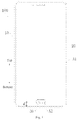
FIG. 1 is a schematic view of an exemplary electronic device according to one embodiment of the present disclosure. -
FIG. 2 is a partial cross-sectional view of the electronic device inFIG. 1 . -
FIG. 3 is a schematic view of an exemplary electronic device according to another embodiment of the present disclosure. -
FIG. 4 is a partial cross-sectional view of the electronic device inFIG. 3 . -
FIG. 5 is a schematic view of an exemplary electronic device according to one embodiment of the present disclosure. -
FIG. 6 is a schematic view of an exemplary electronic device according to another embodiment of the present disclosure. -
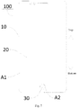
FIG. 7 is a schematic view of an exemplary electronic device according to yet another embodiment of the present disclosure. -
FIG. 8 is a schematic view of an exemplary electronic device according to still another embodiment of the present disclosure. - Below embodiments of the disclosure will be described in detail, examples of which are shown in the accompanying drawings, in which the same or similar reference numerals have been used throughout to denote the same or similar elements or elements serving the same or similar functions. The embodiments described below with reference to the accompanying drawings are exemplary only, meaning they are intended to be illustrative of rather than limiting the disclosure.
- In the specification of the present disclosure, it is to be understood that terms such as "central", "longitudinal", "lateral", "length", "width", "thickness", "upper", "lower", "front", "rear", "left", "right", "vertical", "horizontal", "top", "bottom", "inner", "outer", "clockwise", "counterclockwise", "axial", "radial", and "circumference" refer to the orientations and locational relations illustrated in the drawings, and for describing the present disclosure and for describing in a simple manner, and which are not intended to indicate or imply that the device or the elements are disposed to locate at the specific directions or are structured and performed in the specific directions, which could not to be understood as limiting the present disclosure.
- In addition, terms such as "first" and "second" are used herein for purposes of description and are not intended to indicate or imply relative importance or significance or to imply the number of indicated technical features. Thus, the feature defined with "first" and "second" may include one or more of such a feature. In the description of the present disclosure, "a plurality of' means two or more than two, unless specified otherwise.
- In the present disclosure, unless specified or limited otherwise, terms "mounted", "connected", "coupled", "fixed", and the like are used in a broad sense, and may include, for example, fixed connections, detachable connections, or integral connections; may also be mechanical or electrical connections; may also be direct connections or indirect connections via intervening structures; may also be inner communications of two elements, as can be understood by those skilled in the art depending on specific contexts.
- In the following, an
electronic device 100 provided in embodiments of the present disclosure will be described with reference to drawings. - The
electronic device 100 may include mobile phones, computers or tablet computers, etc. It should be understood that "electronic device 100" in this disclosure can include, but is not limited to, a device that is configured to receive/transmit communication signals via a wireline connection, such as via a public-switched telephone network (PSTN), digital subscriber line (DSL), digital cable, a direct cable connection, and/or another data connection/network, and/or via a wireless interface with, for example, a cellular network, a wireless local area network (WLAN)1 a digital television network such as a DVB-H network, a satellite network, an AM/FM broadcast transmitter, and/or another communication terminal. Examples of theelectronic device 100 include, but are not limited to, a satellite or cellular radiotelephone; a Personal Communications System (PCS) terminal that may combine a cellular radiotelephone with data processing, facsimile and data communications capabilities; a PDA that can include a radiotelephone, pager, Internet/intranet access, Web browser, organizer, calendar and/or a global positioning system (GPS) receiver; and a conventional laptop and/or palmtop receiver or other appliance that includes a radiotelephone transceiver. - Now referring to
FIG. 1 , theelectronic device 100 may include ashell assembly 10, adisplay assembly 20 connected to theshell assembly 10 and afingerprint assembly 30 connected to theshell assembly 10. - The
shell assembly 10 may define a receiving room (not labeled) to receive thedisplay assembly 20 and thefingerprint assembly 30 therein. Thedisplay assembly 20 and thefingerprint assembly 30 may be assembled a whole to be embedded in the receiving room. In addition, a chamber (not labeled) may be defined in theshell assembly 10, to receive some other components such as a battery, a main circuit plate, a camera assembly etc. It should be noted that theshell assembly 10 may be made in one piece. However, theshell assembly 10 can also be integrated with different sections. For example, theshell assembly 10 may be integrated with a first shell and a second shell connected to the first shell. The assembled assembly of thedisplay assembly 20 and thefingerprint assembly 30 may be embedded in the first shell. The other components of theelectronic device 100 may be received in the chamber defined between the first and second shells. Further, various holes may be defined in theshell assembly 10, such as a key hole, an earphone hole, a USB connection hole, a sound hole, a camera mounting hole, a microphone and the like, in order to make theelectronic device 100 be connected with other components. In some embodiments, theshell assembly 10 may be made of metal. Patterns, such as a logo, may be provided on the outside surface of theshell assembly 10, which can improve identification and appearance of theelectronic device 100. In some embodiments, an antenna slot (not shown) may be defined in theshell assembly 10, and it may be communicated with an antenna component inside theshell assembly 10. - The
display assembly 20 may include a display screen 220 (shown inFIG. 2 ). Thedisplay screen 220 may define a first region A1. The first region A1 may be regarded as a display face. The form or shape of the first region A1 may be determined based on the form or shape of thedisplay screen 220, e.g., when thedisplay screen 220 is circular, the first region A1 may be circular and when part of thedisplay screen 220 is curved, the first region A1 corresponding to the part may be a curve. The first region A1 may be configured to display input information from a user, and output information of theelectronic device 100, or various items of theelectronic device 100 for facilitating the user to read related information. - Referring to
FIG. 2 andFIG. 4 , in some embodiments, thedisplay assembly 20 may include asubstrate 210, thedisplay screen 220 attached on thesubstrate 210 and a protectingplate 230 attached on thedisplay screen 220 such that thedisplay screen 220 may be sandwiched between thesubstrate 210 and the protectingplate 230. - The
substrate 210 may be named as cover plate. It can be made of, for example, glass. Thedisplay screen 220 may be attached on thesubstrate 210 to show the input information from the user, and output information of theelectronic device 100, or various items of theelectronic device 100. Thedisplay screen 220 may include a Liquid Crystal Display (LCD), an Organic Light-Emitting Diode (OLED) and the like. - The protecting
plate 230 may be attached on a side of thedisplay screen 220 away from thesubstrate 210. In this way, the protectingplate 230 can protect thedisplay screen 220 from being damaged, resulting in high lifetime of thedisplay assembly 20. In some embodiments, the protectingplate 230 may include glass, which makes manufacturing cost of the protectingplate 230 low. In some embodiments, the protectingplate 230 may include sapphire or tempered (TP) glass, which can improve structural strength of the protectingplate 230. - The
plating plate 230 may define aslot 231. Thefingerprint assembly 30 may be engaged in theslot 231. In some embodiments, theslot 231 may extend through the protectingplate 230 and have a depth h. The depth h may be greater than or equal to 0.5 mm and less than or equal to 0.6 mm. It should be noted that a maximum penetration distance between the user's finger and thefingerprint assembly 30 may be provided. The "maximum penetration distance" can be understood as the maximum thickness that the protectingplate 230 may achieve when thefingerprint assembly 30 is induced with the user's finger passing through the protectingplate 230. The thickness of the protectingplate 230 may be in a range of 0.8 mm ∼ 0.9 mm. When the depth h meets 0.5 mm ≤ h ≤ 0.6 mm, the thickness of a bottom wall of the protectingplate 230 corresponding to theslot 231 may be about 0.3 mm. As is tested, when the user's finger closes to the protectingplate 230 and the distance between the user's finger and thefingerprint assembly 30 is about 0.3 mm, there is a sensitive induction between the user's finger and thefingerprint assembly 30, whereby the reliability and sensitivity of thefingerprint assembly 30 may be improved. Further, the structural strengthen of the protectingplate 230 can be ensured, preventing the protectingplate 230 from being broken due to over pressure. In some embodiments, the thickness of bottom wall of the protectingplate 230 may be 0.28 mm to further improve the sensitivity of thefingerprint assembly 30. The protectingplate 230 may include astep 2311 at theslot 231 to engage with thefingerprint assembly 30. - The
fingerprint assembly 30 may be connected to theshell assembly 10 and located at a side of thedisplay screen 220 away from thesubstrate 210. The connection between thefingerprint assembly 30 and theshell assembly 10 may be direct connections or indirect connections. For example, thefingerprint assembly 30 may be assembled with thedisplay assembly 20 to be integral, then the integral assembly may be assembled with theshell assembly 10. Thus, thefingerprint assembly 30 may be supported and fixed by theshell assembly 10. Thefingerprint assembly 30 may recognize the user's fingerprint information and transmit the information to a control assembly (for example, a processor) of theelectronic device 100 when the user's fingerprint approaches thefingerprint assembly 30. The control assembly may send a corresponding instruction based on the fingerprint information. The fingerprint is unique and cannot change for the lifetime, thereby improving the privacy of theelectronic device 100 due to the provision of thefingerprint assembly 30. - The
fingerprint assembly 30 may be embedded into the protectingplate 230 to facilitate the assembly of thefingerprint assembly 30. As shown inFIG. 2 andFIG. 4 , thefingerprint assembly 30 may include acover 310, thefingerprint chip 320 and fingerprint flexible printed circuit (FPC) 330 which are connected in series. Thecover 310 may be located at a side of thefingerprint chip 320 far away from thesubstrate 210 of thedisplay assembly 20. Thecover 310 may have a circumferential edge engaging (or adhering) with thestep 2311 of thedisplay assembly 20 to cover and protect thefingerprint chip 320 and further improve the stability for thefingerprint assembly 30. Thefingerprint FPC 330 may be connected to the main circuit board of theelectronic device 100. The user's finger and thefingerprint chip 320 may generate induction when the user's fingerprint approaches thefingerprint assembly 30. The induction signal may be transmitted to the control assembly of theelectronic device 100. In some embodiments, thecover 310 may include glass or sapphire. That is, thecover 310 may be made of glass or sapphire. Alternatively, thecover 310 may be a tempered glass plate. - The
fingerprint assembly 30 may have an orthographic projection area on thedisplay screen 220 of thedisplay assembly 20 in a projection direction from the outside to the inside of the electronic device 100 (shown inFIG. 2 andFIG. 4 ). The projection direction is perpendicular to a direction of a contact plane of thefingerprint assembly 30 for contacting with the user's finger; i.e., the projection direction is perpendicular to the finger contact plane of thefingerprint assembly 30. The orthographic projection area may be defined as a second region A2. At least part of the second region A2 may be overlapped with the first region A1. Alternatively, the total second region A2 may be fully located in the first region A1. - Referring to
FIG. 1 andFIG. 8 , a part of the second region A2 may be located in the first region A1 and the other part of the second region A2 may be located outside the first region A1. - It should be noted that at least part of the second region A2 may be overlapped with the first region A1, which means that at least part of the first region A1 may be sheltered by the
fingerprint assembly 30. In other words, the first region A1 may have a region covered by an orthographic projection of thefingerprint assembly 30 on thedisplay assembly 20 when thefingerprint assembly 30 is orthographically projected to thedisplay assembly 20. Therefore, the user cannot view what is displayed where the first region A1 is sheltered or covered by thefingerprint assembly 30. For example, there is some information displayed where the first region A1 is overlapped with the second region A2, but the information may be sheltered by thefingerprint assembly 30. Alternatively, there may be not any information displayed where the first region A1 is overlapped with the second region A2. - In some embodiments, at least part of the second region A2 may overlap with the first region A1, and the second region A2 may have a runway shape. As shown in
FIG. 1 , the runway shape generally includes a rectangle and two semicircles, and the two semicircles are arranged at two ends of the rectangle respectively and opposite to each other. The second region A2 may have a circle configuration, as shown inFIG. 8 . Alternatively, the second region A2 may have other configurations, such as, oval, polygon, etc. - In some embodiments, referring to
FIG. 3 ,FIG. 5 ,FIG. 6 andFIG. 7 , the second region A2 may be fully located in the first region A1. In this instance, an edge of the second region A2 may be in contact with an edge of the first region A1, as shown inFIG. 3 andFIG. 7 . Alternatively, the edge of the second region A2 may not be in contact with the edge of the first region A1, as shown inFIG. 5 andFIG. 6 . - In one embodiment, the second region A2 is fully located in the first region A1 and includes one straight line edge. As shown in
FIG. 3 , the straight line edge may coincide/contact/be level with the lower edge of the first region A1. That is, the first region A1 and the second region A2 may have a line to line contact. Since thefingerprint assembly 30 is embedded in theslot 231 of thedisplay assembly 20, thefingerprint assembly 30 is provided with a corresponding straight line edge flush with the lower edge of the first region A1. In this way, when theshell assembly 10 has a fixed size, a vertical distance d (labeled inFIGS. 1 and3 ) between thedisplay screen 220 of thedisplay assembly 20 and an edge of theshell assembly 10 will be reduced. Thus, the screen-to-body ratio for theelectronic device 100 is increased, improving users' experience. The second region A2 under this instance may have a runway shape, as shown inFIG. 3 . Alternatively, the second region A2 may have a triangle configuration or other configurations having a straight line edge. It is only made sure that the second region A2 totally falls in the first region A1, and the first region A1 and the second region A2 have the line to line contact. - In one embodiment, the second region A2 is fully located in the first region A1, and the first region A1 and the second region A2 have a point to line contact. In detail, the second region A2 contacts with the lower edge of the first region A1. In other words, the second region A2 is tangential to the lower edge of the first region A1. The second region A2 may have a circle configuration, as shown in
FIG. 7 or other configurations tangential to the lower edge of the first region A1. - In other embodiments, the second region A2 is fully located in the first region A1, the second region A2 has none contact with the first region A1, as shown in
FIG. 5 andFIG. 6 . The second region A2 may have a straight line edge substantially parallel with a lower edge with the first region A1, as shownFIG. 5 . The second region A2 may have a runway shape (shown inFIG. 5 ) or circle configuration (shown inFIG. 6 ). In some embodiments, the second region A2 may also have other configurations, such as oval, polygon, etc. - In this disclosure, a display module is further provided. The display module may include the
display assembly 20 and thefingerprint assembly 30 as described previously, which will not be described in detail. - In this disclosure, a display apparatus is further provided, which may include the
display assembly 20 and thefingerprint assembly 30 mentioned previously. - Taking the
electronic device 100 as a mobile phone for an example, in one embodiment, the mobile phone may include theshell assembly 10, thedisplay assembly 20 and thefingerprint assembly 30. The mobile phone may further include a RF circuit, a memory, an input unit, a Wi-Fi module, sensors, audio circuits, a processor and a power supply, which are not illustrated with numbers in drawings. - The RF circuit may be configured to receive and transmit information. In special, the RF circuit sends downlink information to the processor after receiving the downlink information from a base station, and transmits uplink data to the base station. Usually, the RF circuit includes, but is not limited to, an antenna, at least one amplifier, a transceiver, a coupler, a Low Noise Amplifier (LNA), a duplexer and so on. In addition, the RF circuit may further communicate with other devices via wireless communication and a network. The wireless communication may use any one communication standard or protocol, including, but not limited to, Global System of Mobile communication (GSM), General Packet Radio Service (GPRS), Code Division Multiple Access (CDMA), Wideband Code Division Multiple Access (WCDMA), Long Term Evolution (LTE), E-mail, Short Messaging Service (SMS) and so on.
- The memory may be configured to store software programs and modules, and the processor executes various function applications and data processing of the mobile phone by running the software programs and the modules stored in the memory. The memory may mainly include a program storage region and a data storage region, the storage program region may store an operation system, application programs for at least one function (for example, an audio playing function, an image playing function, etc.) and so on; and the data storage region may store data (for example, audio data, telephone directory, etc.) created according to use of the mobile phone. In addition, the memory may include a high-speed RAM, and may further include a non-volatile memory such as one of at least a disk storage device, a flash device, or other non-volatile solid storage devices.
- The input unit may be configured to receive input digital or character information and generate key signal input associated with user setting and functional control of the mobile phone. Specifically, the input unit may include a touch panel and other input devices. The touch panel is also named as touch screen, which is configured to collect touch operations thereon or there-near (such as operations by users' fingers, a touch pen and the like), and drive corresponding connection devices according to preset programs. Optionally, the touch panel may include two parts: a touch detection apparatus and a touch controller. The touch detection apparatus detects a touch operation by a user, converts the detected touch operation into an electrical signal, and transmits the electrical signal to the touch controller. The touch controller receives the electrical signal from the touch detection apparatus, converts the electrical signal into coordinates of a touch point, and then sends the coordinates to the processor. The touch controller may also receive and execute a command sent by the processor. In addition, the touch panel may be a resistive, capacitive, infrared (Infrared), or surface acoustic wave touch panel. The other input devices may include, but are not limited to, one or more of a physical keyboard, a functional key (such as a volume control key and a switch key), a track ball, a mouse, and an operating rod.
- The touch panel can cover the
display screen 220, when the touch operation on or near the touch panel is detected, the touch panel will transmit the touch operation to the processor to determine the type of touch event; thereafter, the processor can provide a corresponding visual output on the display screen according to the type of the touch event. - Audio circuits, speakers, and microphones can provide an audio interface between the user and the phone. The audio circuit can convert the audio data received into electronic signals, and transmit the electronic signals to the speaker, whereby the speaker can convert the electronic signals to sound signals for output. Moreover, a microphone can convert the sound signal received to electronic signals which will be converted into audio data after reception by the audio circuit. The audio circuit output the audio data to the processor, after processing, the processor can transmit the audio data to another mobile phone via the RF circuit, or, the processor can output the audio data to the memory for further process.
- Wi-Fi belongs to a short-range wireless transmission technology, the mobile phone may assist the user in E-mail receiving and sending, webpage browsing, access to streaming media and the like by means of the Wi-Fi module, and it provides a wireless wideband internet access for the user. However, it may be understood that the Wi-Fi module can be optional components of the mobile phone and can totally be omitted without changing the essence of the present disclosure as required.
- The processor is a control center of the mobile phone, and it is configured to connect all parts of the mobile phone by utilizing various interfaces and lines, to run or execute the software program and/or the module stored in the memory and call data stored in the memory to execute various functions and processing data of the mobile phone, so as to wholly monitor the mobile phone. Alternatively, the processor may include one or more processing units. The processor may be integrated with an application processor and a modulation-demodulation processor, the application processor mainly processes an operation system, a user interface, an application program and the like, and the modulation-demodulation processor mainly processes wireless communication. It should be understood that the modulation-demodulation processor may not be integrated into the processor.
- The power supply may be connected with the processor logically via a power supply management system, so as to implement functions of charging, discharging, power consumption management, etc. by means of the power supply management system. The mobile phone may further include a Bluetooth module, a sensor (such as an attitude sensor, a light sensor, an air pressure gage, a humidometer, a temperature gauge or an infrared sensor) and the like, which are not illustrated, and will not be elaborated herein.
- The foregoing disclosed is merely exemplary implementations and it is not intended to limit the scope of the present disclosure; equivalents changes made on the basis of the claims of the present disclosure shall fall into the scope of the present disclosure.
Claims (15)
- A display module, comprising:a display assembly (20), having a display face (A1); anda fingerprint assembly (30), connected to the display assembly (20), characterized in that an orthographic projection area of the fingerprint assembly (30) on the display assembly (20) in a projection direction perpendicular to a finger contact plane of the fingerprint assembly (30) is defined as a second region (A2), and at least part of the second region (A2) is overlapped with the display face (A1).
- The display module of claim 1, wherein the display assembly (20) comprises:a substrate (210); anda display screen (220), attached on the substrate (210) and having the display face (A1);wherein the fingerprint assembly (30) is located at a side of the display screen (220) away from the substrate (210).
- The display module of claim 2, wherein the display assembly (20) further comprises a protecting plate (230) located at the side of the display screen (220) away from the substrate (210), and attached on the display screen (220), wherein the fingerprint assembly (30) is embedded into the protecting plate (230).
- The display module of claim 3, wherein a slot (231) extends through the protecting plate (230), and the fingerprint assembly (30) is engaged in the slot (231).
- The display module of claim 4, wherein the protecting plate (230) comprises a step (2311) at the slot (231) to engage with the fingerprint assembly (30); the fingerprint assembly (30) comprises a cover (310), wherein an edge of the cover (310) is adhered to the step (2311).
- The display module of claim 4 or 5, wherein the slot (231) has a depth greater than or equal to 0.5 mm and less than or equal to 0.6 mm.
- The display module of any one of claims 1-6, wherein an area of a region where the second region (A2) is overlapped with the display face (A1) is defined as S1, and an area of the second region (A2) is defined as S2; a value of S1/S2 is greater than 0, and less than or equal to 1.
- The display module of any one of claims 1-7, wherein the display face (A1) has an upper edge and a lower edge, and a part of an edge of the fingerprint assembly (30) is flush with the lower edge of the display face (A1).
- The display module of claim 8, wherein the second region (A2) has a circle configuration, and the second region (A2) is tangential to the lower edge of the display face (A1).
- The display module of claim 8, wherein the second region (A2) at least comprises one straight edge extending along a line, and the straight edge is flush with the lower edge of the display face (A1).
- The display module of any one of claims 1-8, wherein a shape of the second region (A2) is selected from one of a circle, an oval, a runway shape and a polygon.
- The display module of any one of claims 1-11, wherein the fingerprint assembly (30) shelters at least part of the display screen (220).
- The display module of any one of claims 1-12, wherein the display screen (220) is configured to show information needing to be displayed, the fingerprint assembly (30) is totally located above the display screen (220).
- The display module of any one of claims 1-13, wherein the fingerprint assembly (30) comprises a cover (310), a fingerprint chip (320) and a fingerprint FPC (330) which are connected in series.
- An electronic device (100), characterized by comprising a shell assembly (10) and the display module as claimed in any one of claims 1-14, wherein the display assembly (20) is connected to the shell assembly (10).
Applications Claiming Priority (2)
| Application Number | Priority Date | Filing Date | Title |
|---|---|---|---|
| CN201720898888.4U CN207184551U (en) | 2017-07-21 | 2017-07-21 | Electronic equipment and display modules |
| CN201710598947.0A CN107332949A (en) | 2017-07-21 | 2017-07-21 | Electronic equipment and display module |
Publications (2)
| Publication Number | Publication Date |
|---|---|
| EP3432200A1 true EP3432200A1 (en) | 2019-01-23 |
| EP3432200B1 EP3432200B1 (en) | 2023-10-25 |
Family
ID=62528324
Family Applications (1)
| Application Number | Title | Priority Date | Filing Date |
|---|---|---|---|
| EP18175739.4A Active EP3432200B1 (en) | 2017-07-21 | 2018-06-04 | Display module and electronic device |
Country Status (3)
| Country | Link |
|---|---|
| US (1) | US10409329B2 (en) |
| EP (1) | EP3432200B1 (en) |
| WO (1) | WO2019015401A1 (en) |
Families Citing this family (3)
| Publication number | Priority date | Publication date | Assignee | Title |
|---|---|---|---|---|
| CN209964141U (en) * | 2019-04-19 | 2020-01-17 | Oppo广东移动通信有限公司 | Mobile terminal and shell assembly thereof |
| KR102872890B1 (en) * | 2019-12-04 | 2025-10-16 | 엘지디스플레이 주식회사 | Flexible display device |
| CN114244940A (en) * | 2022-01-11 | 2022-03-25 | Oppo广东移动通信有限公司 | Under-screen identification components and electronic equipment |
Citations (5)
| Publication number | Priority date | Publication date | Assignee | Title |
|---|---|---|---|---|
| CN203838722U (en) * | 2014-04-04 | 2014-09-17 | 深圳印象认知技术有限公司 | Liquid crystal terminal equipment and fingerprint acquisition device |
| US20150036065A1 (en) * | 2013-08-05 | 2015-02-05 | Apple Inc. | Fingerprint Sensor in an Electronic Device |
| US20150177884A1 (en) * | 2013-12-23 | 2015-06-25 | Samsung Electronics Co., Ltd. | Apparatus for sensing touch input in electronic device |
| US20150254491A1 (en) * | 2014-03-07 | 2015-09-10 | Focaltech Systems, Ltd. | Display device, driving circuit, method for driving display device, and electronic apparatus |
| US9710689B2 (en) * | 2015-10-30 | 2017-07-18 | Essential Products, Inc. | Fingerprint sensors for mobile devices |
Family Cites Families (18)
| Publication number | Priority date | Publication date | Assignee | Title |
|---|---|---|---|---|
| US6876056B2 (en) * | 2001-04-19 | 2005-04-05 | Interuniversitair Microelektronica Centrum (Imec) | Method and system for fabrication of integrated tunable/switchable passive microwave and millimeter wave modules |
| JP2002366056A (en) * | 2001-06-07 | 2002-12-20 | Casio Comput Co Ltd | Display device |
| JP4196888B2 (en) * | 2004-06-25 | 2008-12-17 | セイコーエプソン株式会社 | Electro-optical device and electronic apparatus |
| JP4581726B2 (en) * | 2004-12-28 | 2010-11-17 | ソニー株式会社 | Display device and portable device |
| KR20090077755A (en) * | 2006-09-09 | 2009-07-15 | 에프-오리진, 인크. | Integrated Pressure Sensing Lens Assembly |
| KR101372815B1 (en) * | 2007-04-02 | 2014-03-14 | 삼성디스플레이 주식회사 | Liquid crystal display module |
| US9336428B2 (en) * | 2009-10-30 | 2016-05-10 | Synaptics Incorporated | Integrated fingerprint sensor and display |
| US20130265256A1 (en) * | 2012-04-07 | 2013-10-10 | Cambridge Touch Technologies, Ltd. | Pressure sensing display device |
| US9886613B2 (en) * | 2014-07-07 | 2018-02-06 | Shenzhen GOODIX Technology Co., Ltd. | Integration of touch screen and fingerprint sensor assembly |
| CN208044621U (en) * | 2014-12-11 | 2018-11-02 | 韩国科泰高科株式会社 | Electronic device cover window integrated fingerprint sensor module assembly |
| WO2016144108A1 (en) * | 2015-03-10 | 2016-09-15 | 크루셜텍 (주) | Display device capable of scanning images |
| KR102415651B1 (en) * | 2015-07-01 | 2022-07-01 | 엘지전자 주식회사 | Mobile terminal |
| CN105225872B (en) * | 2015-09-25 | 2017-11-10 | 维沃移动通信有限公司 | A kind of press-key structure and electronic equipment |
| CN107741759A (en) * | 2016-07-26 | 2018-02-27 | 广东欧珀移动通信有限公司 | Mobile terminal, housing assembly, display assembly and assembly method thereof |
| KR102013053B1 (en) * | 2016-09-29 | 2019-08-21 | 선전 구딕스 테크놀로지 컴퍼니, 리미티드 | Screen assembly with a fingerprint module and electronic device |
| CN206313842U (en) * | 2017-01-10 | 2017-07-07 | 广东欧珀移动通信有限公司 | Display screen component and mobile terminal |
| CN107332949A (en) * | 2017-07-21 | 2017-11-07 | 广东欧珀移动通信有限公司 | Electronic equipment and display module |
| CN207184551U (en) * | 2017-07-21 | 2018-04-03 | 广东欧珀移动通信有限公司 | Electronic equipment and display modules |
-
2018
- 2018-05-28 WO PCT/CN2018/088731 patent/WO2019015401A1/en not_active Ceased
- 2018-06-04 EP EP18175739.4A patent/EP3432200B1/en active Active
- 2018-06-27 US US16/020,439 patent/US10409329B2/en active Active
Patent Citations (5)
| Publication number | Priority date | Publication date | Assignee | Title |
|---|---|---|---|---|
| US20150036065A1 (en) * | 2013-08-05 | 2015-02-05 | Apple Inc. | Fingerprint Sensor in an Electronic Device |
| US20150177884A1 (en) * | 2013-12-23 | 2015-06-25 | Samsung Electronics Co., Ltd. | Apparatus for sensing touch input in electronic device |
| US20150254491A1 (en) * | 2014-03-07 | 2015-09-10 | Focaltech Systems, Ltd. | Display device, driving circuit, method for driving display device, and electronic apparatus |
| CN203838722U (en) * | 2014-04-04 | 2014-09-17 | 深圳印象认知技术有限公司 | Liquid crystal terminal equipment and fingerprint acquisition device |
| US9710689B2 (en) * | 2015-10-30 | 2017-07-18 | Essential Products, Inc. | Fingerprint sensors for mobile devices |
Also Published As
| Publication number | Publication date |
|---|---|
| US10409329B2 (en) | 2019-09-10 |
| US20190025884A1 (en) | 2019-01-24 |
| EP3432200B1 (en) | 2023-10-25 |
| WO2019015401A1 (en) | 2019-01-24 |
Similar Documents
| Publication | Publication Date | Title |
|---|---|---|
| US10623542B2 (en) | Display assembly and mobile terminal | |
| WO2019091380A1 (en) | Camera device, bracket and mobile terminal using same | |
| EP3343886B1 (en) | Bracket for mounting fingerprint identification assembly, cover plate assembly and terminal | |
| EP3432200B1 (en) | Display module and electronic device | |
| CN111989906B (en) | Electronic device | |
| CN207039679U (en) | Electronic equipment | |
| CN107332949A (en) | Electronic equipment and display module | |
| CN108229374B (en) | Fingerprint module, manufacturing method of fingerprint module, and electronic device | |
| CN208386611U (en) | Electronic equipment | |
| CN111447352B (en) | Brackets, camera components and terminal equipment | |
| WO2019201217A1 (en) | Electronic device | |
| US10368450B2 (en) | Housing assembly for electronic device and electronic device | |
| EP3518510B1 (en) | Frame assembly, housing and electronic device having the same | |
| CN207184551U (en) | Electronic equipment and display modules | |
| US10880418B2 (en) | Housing assembly for terminal and terminal with housing assembly | |
| EP3370398B1 (en) | Shell assembly, electronic device and mobile phone having same | |
| CN214754106U (en) | Antenna Shrapnel and Electronic Equipment | |
| CN212209297U (en) | Terminal equipment and its housing components | |
| CN121864901A (en) | Side key support and intelligent terminal | |
| CN113261264A (en) | Shell assembly and mobile terminal | |
| HK1246537A1 (en) | Electronic equipment and display module | |
| HK1246537A (en) | Electronic equipment and display module | |
| WO2018205808A1 (en) | Housing component of electronic device, and electronic device having same | |
| HK40009396A (en) | Mobile terminal and shell and middle frame structure thereof | |
| CN111029730A (en) | Antenna structure and mobile terminal |
Legal Events
| Date | Code | Title | Description |
|---|---|---|---|
| PUAI | Public reference made under article 153(3) epc to a published international application that has entered the european phase |
Free format text: ORIGINAL CODE: 0009012 |
|
| STAA | Information on the status of an ep patent application or granted ep patent |
Free format text: STATUS: THE APPLICATION HAS BEEN PUBLISHED |
|
| AK | Designated contracting states |
Kind code of ref document: A1 Designated state(s): AL AT BE BG CH CY CZ DE DK EE ES FI FR GB GR HR HU IE IS IT LI LT LU LV MC MK MT NL NO PL PT RO RS SE SI SK SM TR |
|
| AX | Request for extension of the european patent |
Extension state: BA ME |
|
| STAA | Information on the status of an ep patent application or granted ep patent |
Free format text: STATUS: REQUEST FOR EXAMINATION WAS MADE |
|
| 17P | Request for examination filed |
Effective date: 20190515 |
|
| RBV | Designated contracting states (corrected) |
Designated state(s): AL AT BE BG CH CY CZ DE DK EE ES FI FR GB GR HR HU IE IS IT LI LT LU LV MC MK MT NL NO PL PT RO RS SE SI SK SM TR |
|
| RAP1 | Party data changed (applicant data changed or rights of an application transferred) |
Owner name: GUANGDONG OPPO MOBILE TELECOMMUNICATIONS CORP., LT |
|
| STAA | Information on the status of an ep patent application or granted ep patent |
Free format text: STATUS: EXAMINATION IS IN PROGRESS |
|
| 17Q | First examination report despatched |
Effective date: 20200929 |
|
| REG | Reference to a national code |
Ref country code: DE Ref legal event code: R079 Free format text: PREVIOUS MAIN CLASS: G06K0009000000 Ipc: G06V0040130000 Ref country code: DE Ref legal event code: R079 Ref document number: 602018059837 Country of ref document: DE Free format text: PREVIOUS MAIN CLASS: G06K0009000000 Ipc: G06V0040130000 |
|
| GRAP | Despatch of communication of intention to grant a patent |
Free format text: ORIGINAL CODE: EPIDOSNIGR1 |
|
| STAA | Information on the status of an ep patent application or granted ep patent |
Free format text: STATUS: GRANT OF PATENT IS INTENDED |
|
| RIC1 | Information provided on ipc code assigned before grant |
Ipc: G06V 40/13 20220101AFI20230705BHEP |
|
| INTG | Intention to grant announced |
Effective date: 20230721 |
|
| GRAS | Grant fee paid |
Free format text: ORIGINAL CODE: EPIDOSNIGR3 |
|
| GRAA | (expected) grant |
Free format text: ORIGINAL CODE: 0009210 |
|
| STAA | Information on the status of an ep patent application or granted ep patent |
Free format text: STATUS: THE PATENT HAS BEEN GRANTED |
|
| AK | Designated contracting states |
Kind code of ref document: B1 Designated state(s): AL AT BE BG CH CY CZ DE DK EE ES FI FR GB GR HR HU IE IS IT LI LT LU LV MC MK MT NL NO PL PT RO RS SE SI SK SM TR |
|
| REG | Reference to a national code |
Ref country code: GB Ref legal event code: FG4D |
|
| REG | Reference to a national code |
Ref country code: CH Ref legal event code: EP |
|
| REG | Reference to a national code |
Ref country code: DE Ref legal event code: R096 Ref document number: 602018059837 Country of ref document: DE |
|
| REG | Reference to a national code |
Ref country code: IE Ref legal event code: FG4D |
|
| REG | Reference to a national code |
Ref country code: LT Ref legal event code: MG9D |
|
| P01 | Opt-out of the competence of the unified patent court (upc) registered |
Effective date: 20240110 |
|
| REG | Reference to a national code |
Ref country code: NL Ref legal event code: MP Effective date: 20231025 |
|
| REG | Reference to a national code |
Ref country code: AT Ref legal event code: MK05 Ref document number: 1625478 Country of ref document: AT Kind code of ref document: T Effective date: 20231025 |
|
| PG25 | Lapsed in a contracting state [announced via postgrant information from national office to epo] |
Ref country code: NL Free format text: LAPSE BECAUSE OF FAILURE TO SUBMIT A TRANSLATION OF THE DESCRIPTION OR TO PAY THE FEE WITHIN THE PRESCRIBED TIME-LIMIT Effective date: 20231025 |
|
| PG25 | Lapsed in a contracting state [announced via postgrant information from national office to epo] |
Ref country code: GR Free format text: LAPSE BECAUSE OF FAILURE TO SUBMIT A TRANSLATION OF THE DESCRIPTION OR TO PAY THE FEE WITHIN THE PRESCRIBED TIME-LIMIT Effective date: 20240126 |
|
| PG25 | Lapsed in a contracting state [announced via postgrant information from national office to epo] |
Ref country code: IS Free format text: LAPSE BECAUSE OF FAILURE TO SUBMIT A TRANSLATION OF THE DESCRIPTION OR TO PAY THE FEE WITHIN THE PRESCRIBED TIME-LIMIT Effective date: 20240225 |
|
| PG25 | Lapsed in a contracting state [announced via postgrant information from national office to epo] |
Ref country code: LT Free format text: LAPSE BECAUSE OF FAILURE TO SUBMIT A TRANSLATION OF THE DESCRIPTION OR TO PAY THE FEE WITHIN THE PRESCRIBED TIME-LIMIT Effective date: 20231025 |
|
| PG25 | Lapsed in a contracting state [announced via postgrant information from national office to epo] |
Ref country code: AT Free format text: LAPSE BECAUSE OF FAILURE TO SUBMIT A TRANSLATION OF THE DESCRIPTION OR TO PAY THE FEE WITHIN THE PRESCRIBED TIME-LIMIT Effective date: 20231025 |
|
| PG25 | Lapsed in a contracting state [announced via postgrant information from national office to epo] |
Ref country code: ES Free format text: LAPSE BECAUSE OF FAILURE TO SUBMIT A TRANSLATION OF THE DESCRIPTION OR TO PAY THE FEE WITHIN THE PRESCRIBED TIME-LIMIT Effective date: 20231025 |
|
| PG25 | Lapsed in a contracting state [announced via postgrant information from national office to epo] |
Ref country code: LT Free format text: LAPSE BECAUSE OF FAILURE TO SUBMIT A TRANSLATION OF THE DESCRIPTION OR TO PAY THE FEE WITHIN THE PRESCRIBED TIME-LIMIT Effective date: 20231025 Ref country code: IS Free format text: LAPSE BECAUSE OF FAILURE TO SUBMIT A TRANSLATION OF THE DESCRIPTION OR TO PAY THE FEE WITHIN THE PRESCRIBED TIME-LIMIT Effective date: 20240225 Ref country code: GR Free format text: LAPSE BECAUSE OF FAILURE TO SUBMIT A TRANSLATION OF THE DESCRIPTION OR TO PAY THE FEE WITHIN THE PRESCRIBED TIME-LIMIT Effective date: 20240126 Ref country code: ES Free format text: LAPSE BECAUSE OF FAILURE TO SUBMIT A TRANSLATION OF THE DESCRIPTION OR TO PAY THE FEE WITHIN THE PRESCRIBED TIME-LIMIT Effective date: 20231025 Ref country code: BG Free format text: LAPSE BECAUSE OF FAILURE TO SUBMIT A TRANSLATION OF THE DESCRIPTION OR TO PAY THE FEE WITHIN THE PRESCRIBED TIME-LIMIT Effective date: 20240125 Ref country code: AT Free format text: LAPSE BECAUSE OF FAILURE TO SUBMIT A TRANSLATION OF THE DESCRIPTION OR TO PAY THE FEE WITHIN THE PRESCRIBED TIME-LIMIT Effective date: 20231025 Ref country code: PT Free format text: LAPSE BECAUSE OF FAILURE TO SUBMIT A TRANSLATION OF THE DESCRIPTION OR TO PAY THE FEE WITHIN THE PRESCRIBED TIME-LIMIT Effective date: 20240226 |
|
| PG25 | Lapsed in a contracting state [announced via postgrant information from national office to epo] |
Ref country code: SE Free format text: LAPSE BECAUSE OF FAILURE TO SUBMIT A TRANSLATION OF THE DESCRIPTION OR TO PAY THE FEE WITHIN THE PRESCRIBED TIME-LIMIT Effective date: 20231025 Ref country code: RS Free format text: LAPSE BECAUSE OF FAILURE TO SUBMIT A TRANSLATION OF THE DESCRIPTION OR TO PAY THE FEE WITHIN THE PRESCRIBED TIME-LIMIT Effective date: 20231025 Ref country code: PL Free format text: LAPSE BECAUSE OF FAILURE TO SUBMIT A TRANSLATION OF THE DESCRIPTION OR TO PAY THE FEE WITHIN THE PRESCRIBED TIME-LIMIT Effective date: 20231025 Ref country code: NO Free format text: LAPSE BECAUSE OF FAILURE TO SUBMIT A TRANSLATION OF THE DESCRIPTION OR TO PAY THE FEE WITHIN THE PRESCRIBED TIME-LIMIT Effective date: 20240125 Ref country code: LV Free format text: LAPSE BECAUSE OF FAILURE TO SUBMIT A TRANSLATION OF THE DESCRIPTION OR TO PAY THE FEE WITHIN THE PRESCRIBED TIME-LIMIT Effective date: 20231025 Ref country code: HR Free format text: LAPSE BECAUSE OF FAILURE TO SUBMIT A TRANSLATION OF THE DESCRIPTION OR TO PAY THE FEE WITHIN THE PRESCRIBED TIME-LIMIT Effective date: 20231025 |
|
| PG25 | Lapsed in a contracting state [announced via postgrant information from national office to epo] |
Ref country code: DK Free format text: LAPSE BECAUSE OF FAILURE TO SUBMIT A TRANSLATION OF THE DESCRIPTION OR TO PAY THE FEE WITHIN THE PRESCRIBED TIME-LIMIT Effective date: 20231025 |
|
| PG25 | Lapsed in a contracting state [announced via postgrant information from national office to epo] |
Ref country code: CZ Free format text: LAPSE BECAUSE OF FAILURE TO SUBMIT A TRANSLATION OF THE DESCRIPTION OR TO PAY THE FEE WITHIN THE PRESCRIBED TIME-LIMIT Effective date: 20231025 |
|
| REG | Reference to a national code |
Ref country code: DE Ref legal event code: R097 Ref document number: 602018059837 Country of ref document: DE |
|
| PG25 | Lapsed in a contracting state [announced via postgrant information from national office to epo] |
Ref country code: SK Free format text: LAPSE BECAUSE OF FAILURE TO SUBMIT A TRANSLATION OF THE DESCRIPTION OR TO PAY THE FEE WITHIN THE PRESCRIBED TIME-LIMIT Effective date: 20231025 |
|
| PG25 | Lapsed in a contracting state [announced via postgrant information from national office to epo] |
Ref country code: SM Free format text: LAPSE BECAUSE OF FAILURE TO SUBMIT A TRANSLATION OF THE DESCRIPTION OR TO PAY THE FEE WITHIN THE PRESCRIBED TIME-LIMIT Effective date: 20231025 Ref country code: SK Free format text: LAPSE BECAUSE OF FAILURE TO SUBMIT A TRANSLATION OF THE DESCRIPTION OR TO PAY THE FEE WITHIN THE PRESCRIBED TIME-LIMIT Effective date: 20231025 Ref country code: RO Free format text: LAPSE BECAUSE OF FAILURE TO SUBMIT A TRANSLATION OF THE DESCRIPTION OR TO PAY THE FEE WITHIN THE PRESCRIBED TIME-LIMIT Effective date: 20231025 Ref country code: IT Free format text: LAPSE BECAUSE OF FAILURE TO SUBMIT A TRANSLATION OF THE DESCRIPTION OR TO PAY THE FEE WITHIN THE PRESCRIBED TIME-LIMIT Effective date: 20231025 Ref country code: EE Free format text: LAPSE BECAUSE OF FAILURE TO SUBMIT A TRANSLATION OF THE DESCRIPTION OR TO PAY THE FEE WITHIN THE PRESCRIBED TIME-LIMIT Effective date: 20231025 Ref country code: DK Free format text: LAPSE BECAUSE OF FAILURE TO SUBMIT A TRANSLATION OF THE DESCRIPTION OR TO PAY THE FEE WITHIN THE PRESCRIBED TIME-LIMIT Effective date: 20231025 Ref country code: CZ Free format text: LAPSE BECAUSE OF FAILURE TO SUBMIT A TRANSLATION OF THE DESCRIPTION OR TO PAY THE FEE WITHIN THE PRESCRIBED TIME-LIMIT Effective date: 20231025 |
|
| PLBE | No opposition filed within time limit |
Free format text: ORIGINAL CODE: 0009261 |
|
| STAA | Information on the status of an ep patent application or granted ep patent |
Free format text: STATUS: NO OPPOSITION FILED WITHIN TIME LIMIT |
|
| 26N | No opposition filed |
Effective date: 20240726 |
|
| PG25 | Lapsed in a contracting state [announced via postgrant information from national office to epo] |
Ref country code: SI Free format text: LAPSE BECAUSE OF FAILURE TO SUBMIT A TRANSLATION OF THE DESCRIPTION OR TO PAY THE FEE WITHIN THE PRESCRIBED TIME-LIMIT Effective date: 20231025 |
|
| PG25 | Lapsed in a contracting state [announced via postgrant information from national office to epo] |
Ref country code: SI Free format text: LAPSE BECAUSE OF FAILURE TO SUBMIT A TRANSLATION OF THE DESCRIPTION OR TO PAY THE FEE WITHIN THE PRESCRIBED TIME-LIMIT Effective date: 20231025 |
|
| REG | Reference to a national code |
Ref country code: DE Ref legal event code: R119 Ref document number: 602018059837 Country of ref document: DE |
|
| PG25 | Lapsed in a contracting state [announced via postgrant information from national office to epo] |
Ref country code: MC Free format text: LAPSE BECAUSE OF FAILURE TO SUBMIT A TRANSLATION OF THE DESCRIPTION OR TO PAY THE FEE WITHIN THE PRESCRIBED TIME-LIMIT Effective date: 20231025 |
|
| REG | Reference to a national code |
Ref country code: CH Ref legal event code: PL |
|
| PG25 | Lapsed in a contracting state [announced via postgrant information from national office to epo] |
Ref country code: LU Free format text: LAPSE BECAUSE OF NON-PAYMENT OF DUE FEES Effective date: 20240604 |
|
| GBPC | Gb: european patent ceased through non-payment of renewal fee |
Effective date: 20240604 |
|
| PG25 | Lapsed in a contracting state [announced via postgrant information from national office to epo] |
Ref country code: DE Free format text: LAPSE BECAUSE OF NON-PAYMENT OF DUE FEES Effective date: 20250101 |
|
| PG25 | Lapsed in a contracting state [announced via postgrant information from national office to epo] |
Ref country code: IE Free format text: LAPSE BECAUSE OF NON-PAYMENT OF DUE FEES Effective date: 20240604 |
|
| PG25 | Lapsed in a contracting state [announced via postgrant information from national office to epo] |
Ref country code: CH Free format text: LAPSE BECAUSE OF NON-PAYMENT OF DUE FEES Effective date: 20240630 Ref country code: BE Free format text: LAPSE BECAUSE OF NON-PAYMENT OF DUE FEES Effective date: 20240630 |
|
| PG25 | Lapsed in a contracting state [announced via postgrant information from national office to epo] |
Ref country code: FR Free format text: LAPSE BECAUSE OF NON-PAYMENT OF DUE FEES Effective date: 20240630 |
|
| PG25 | Lapsed in a contracting state [announced via postgrant information from national office to epo] |
Ref country code: GB Free format text: LAPSE BECAUSE OF NON-PAYMENT OF DUE FEES Effective date: 20240604 |
|
| REG | Reference to a national code |
Ref country code: BE Ref legal event code: MM Effective date: 20240630 |
|
| PG25 | Lapsed in a contracting state [announced via postgrant information from national office to epo] |
Ref country code: FI Free format text: LAPSE BECAUSE OF FAILURE TO SUBMIT A TRANSLATION OF THE DESCRIPTION OR TO PAY THE FEE WITHIN THE PRESCRIBED TIME-LIMIT Effective date: 20231025 |
|
| PG25 | Lapsed in a contracting state [announced via postgrant information from national office to epo] |
Ref country code: CY Free format text: LAPSE BECAUSE OF FAILURE TO SUBMIT A TRANSLATION OF THE DESCRIPTION OR TO PAY THE FEE WITHIN THE PRESCRIBED TIME-LIMIT; INVALID AB INITIO Effective date: 20180604 |
|
| PG25 | Lapsed in a contracting state [announced via postgrant information from national office to epo] |
Ref country code: HU Free format text: LAPSE BECAUSE OF FAILURE TO SUBMIT A TRANSLATION OF THE DESCRIPTION OR TO PAY THE FEE WITHIN THE PRESCRIBED TIME-LIMIT; INVALID AB INITIO Effective date: 20180604 |