EP3432118A1 - Add-on processing unit with i/o connectors - Google Patents
Add-on processing unit with i/o connectors Download PDFInfo
- Publication number
- EP3432118A1 EP3432118A1 EP18175327.8A EP18175327A EP3432118A1 EP 3432118 A1 EP3432118 A1 EP 3432118A1 EP 18175327 A EP18175327 A EP 18175327A EP 3432118 A1 EP3432118 A1 EP 3432118A1
- Authority
- EP
- European Patent Office
- Prior art keywords
- circuit card
- connector
- assembly
- bracket
- card assembly
- Prior art date
- Legal status (The legal status is an assumption and is not a legal conclusion. Google has not performed a legal analysis and makes no representation as to the accuracy of the status listed.)
- Granted
Links
Images




Classifications
-
- G—PHYSICS
- G06—COMPUTING OR CALCULATING; COUNTING
- G06F—ELECTRIC DIGITAL DATA PROCESSING
- G06F1/00—Details not covered by groups G06F3/00 - G06F13/00 and G06F21/00
- G06F1/16—Constructional details or arrangements
- G06F1/18—Packaging or power distribution
- G06F1/183—Internal mounting support structures, e.g. for supporting printed circuit boards
- G06F1/185—Mounting of expansion boards
-
- H—ELECTRICITY
- H01—ELECTRIC ELEMENTS
- H01R—ELECTRICALLY-CONDUCTIVE CONNECTIONS; STRUCTURAL ASSOCIATIONS OF A PLURALITY OF MUTUALLY-INSULATED ELECTRICAL CONNECTING ELEMENTS; COUPLING DEVICES; CURRENT COLLECTORS
- H01R12/00—Structural associations of a plurality of mutually-insulated electrical connecting elements, specially adapted for printed circuits, e.g. printed circuit boards [PCB], flat or ribbon cables, or like generally planar structures, e.g. terminal strips, terminal blocks; Coupling devices specially adapted for printed circuits, flat or ribbon cables, or like generally planar structures; Terminals specially adapted for contact with, or insertion into, printed circuits, flat or ribbon cables, or like generally planar structures
- H01R12/70—Coupling devices
- H01R12/71—Coupling devices for rigid printing circuits or like structures
- H01R12/72—Coupling devices for rigid printing circuits or like structures coupling with the edge of the rigid printed circuits or like structures
- H01R12/721—Coupling devices for rigid printing circuits or like structures coupling with the edge of the rigid printed circuits or like structures cooperating directly with the edge of the rigid printed circuits
-
- G—PHYSICS
- G06—COMPUTING OR CALCULATING; COUNTING
- G06F—ELECTRIC DIGITAL DATA PROCESSING
- G06F1/00—Details not covered by groups G06F3/00 - G06F13/00 and G06F21/00
- G06F1/16—Constructional details or arrangements
- G06F1/18—Packaging or power distribution
- G06F1/183—Internal mounting support structures, e.g. for supporting printed circuit boards
- G06F1/185—Mounting of expansion boards
- G06F1/186—Securing of expansion boards in correspondence to slots provided at the computer enclosure
-
- G—PHYSICS
- G06—COMPUTING OR CALCULATING; COUNTING
- G06F—ELECTRIC DIGITAL DATA PROCESSING
- G06F1/00—Details not covered by groups G06F3/00 - G06F13/00 and G06F21/00
- G06F1/16—Constructional details or arrangements
- G06F1/20—Cooling means
-
- G—PHYSICS
- G06—COMPUTING OR CALCULATING; COUNTING
- G06F—ELECTRIC DIGITAL DATA PROCESSING
- G06F13/00—Interconnection of, or transfer of information or other signals between, memories, input/output devices or central processing units
- G06F13/38—Information transfer, e.g. on bus
- G06F13/40—Bus structure
- G06F13/4063—Device-to-bus coupling
- G06F13/409—Mechanical coupling
-
- G—PHYSICS
- G06—COMPUTING OR CALCULATING; COUNTING
- G06T—IMAGE DATA PROCESSING OR GENERATION, IN GENERAL
- G06T1/00—General purpose image data processing
- G06T1/20—Processor architectures; Processor configuration, e.g. pipelining
-
- H—ELECTRICITY
- H01—ELECTRIC ELEMENTS
- H01R—ELECTRICALLY-CONDUCTIVE CONNECTIONS; STRUCTURAL ASSOCIATIONS OF A PLURALITY OF MUTUALLY-INSULATED ELECTRICAL CONNECTING ELEMENTS; COUPLING DEVICES; CURRENT COLLECTORS
- H01R12/00—Structural associations of a plurality of mutually-insulated electrical connecting elements, specially adapted for printed circuits, e.g. printed circuit boards [PCB], flat or ribbon cables, or like generally planar structures, e.g. terminal strips, terminal blocks; Coupling devices specially adapted for printed circuits, flat or ribbon cables, or like generally planar structures; Terminals specially adapted for contact with, or insertion into, printed circuits, flat or ribbon cables, or like generally planar structures
- H01R12/50—Fixed connections
- H01R12/59—Fixed connections for flexible printed circuits, flat or ribbon cables or like structures
- H01R12/65—Fixed connections for flexible printed circuits, flat or ribbon cables or like structures characterised by the terminal
- H01R12/67—Fixed connections for flexible printed circuits, flat or ribbon cables or like structures characterised by the terminal insulation penetrating terminals
- H01R12/675—Fixed connections for flexible printed circuits, flat or ribbon cables or like structures characterised by the terminal insulation penetrating terminals with contacts having at least a slotted plate for penetration of cable insulation, e.g. insulation displacement contacts for round conductor flat cables
-
- H—ELECTRICITY
- H01—ELECTRIC ELEMENTS
- H01R—ELECTRICALLY-CONDUCTIVE CONNECTIONS; STRUCTURAL ASSOCIATIONS OF A PLURALITY OF MUTUALLY-INSULATED ELECTRICAL CONNECTING ELEMENTS; COUPLING DEVICES; CURRENT COLLECTORS
- H01R12/00—Structural associations of a plurality of mutually-insulated electrical connecting elements, specially adapted for printed circuits, e.g. printed circuit boards [PCB], flat or ribbon cables, or like generally planar structures, e.g. terminal strips, terminal blocks; Coupling devices specially adapted for printed circuits, flat or ribbon cables, or like generally planar structures; Terminals specially adapted for contact with, or insertion into, printed circuits, flat or ribbon cables, or like generally planar structures
- H01R12/70—Coupling devices
- H01R12/7082—Coupling device supported only by cooperation with PCB
-
- H—ELECTRICITY
- H05—ELECTRIC TECHNIQUES NOT OTHERWISE PROVIDED FOR
- H05K—PRINTED CIRCUITS; CASINGS OR CONSTRUCTIONAL DETAILS OF ELECTRIC APPARATUS; MANUFACTURE OF ASSEMBLAGES OF ELECTRICAL COMPONENTS
- H05K7/00—Constructional details common to different types of electric apparatus
- H05K7/14—Mounting supporting structure in casing or on frame or rack
- H05K7/1485—Servers; Data center rooms, e.g. 19-inch computer racks
- H05K7/1487—Blade assemblies, e.g. blade cases or inner arrangements within a blade
-
- H—ELECTRICITY
- H01—ELECTRIC ELEMENTS
- H01R—ELECTRICALLY-CONDUCTIVE CONNECTIONS; STRUCTURAL ASSOCIATIONS OF A PLURALITY OF MUTUALLY-INSULATED ELECTRICAL CONNECTING ELEMENTS; COUPLING DEVICES; CURRENT COLLECTORS
- H01R2201/00—Connectors or connections adapted for particular applications
- H01R2201/06—Connectors or connections adapted for particular applications for computer periphery
Definitions
- the present invention relates to add-on processing units, and more specifically to apparatus and methods for assembling add-on units with input/output connectors.
- a graphics processing unit which typically handles computation only for computer graphics, is configured to perform computation in applications traditionally handled by the central processing unit (CPU).
- CPU central processing unit
- a GPGPU unit analyzes data from the CPU as if it were in image or other graphic form.
- GPUs operate at lower frequencies than CPUs, they typically have many times the number of cores.
- GPUs can operate on pictures and graphical data at far faster rates than traditional CPUs. Consequently, migrating data into graphical form, and then using the GPU to scan and analyze it, can result in significant improvements in computation time.
- GPGPU units have been investigated for improve throughput in communications applications.
- a GPGPU unit can be configured to perform communications and signal processing functions at a much higher throughput or data rate that a traditional CPU.
- a GPGPU unit can significantly improve throughput in many types of transceiver systems.
- GPGPU unit may offer computational advantages, implementing a communications GPGPU unit is far from trivial.
- traditional GPGPU unit design does not typically include input/output (I/O) ports that would be necessary for a communications-based GPGPU unit to operate efficiently.
- I/O input/output
- the high performance of GPGPU unit comes at a high thermal cost, resulting in most GPGPU units running at relatively high temperatures (typically 80°C-85°C). As a result, these high temperatures do not provide an adequate environment for communication of certain types of signals (e.g., optical signals).
- GPGPU unit designs incorporating I/O ports typically require specialized connection and mounting schemes, thereby providing limited backward compatibility with older chassis support traditional form factor designs for add-on cards.
- Embodiments concern a circuit card assembly defining an add-on processing unit with I/O connectors.
- a circuit card assembly according to a first embodiment is configured for removable attachment to a computer system having a plurality of bracket slots arranged with a fixed pitch.
- the circuit card assembly includes a circuit card having a front end, a back end, and substantially parallel longitudinal edges between the front end and the back end.
- the circuit card includes at least one bus connector extending from one of the longitudinal edges.
- the circuit card assembly also includes a bracket structure that provides a mounting surface at the front end of said circuit card.
- the mounting surface extends perpendicularly to a first surface of said circuit card and extends perpendicularly to said longitudinal edges.
- the mounting surface comprises a bracket for engaging with a plurality of adjacent ones of the plurality of bracket slots.
- the circuit card assembly also includes a connector assembly disposed on the first surface of said circuit card at said front end.
- the connector assembly includes a first input/output (I/O) connector and a second I/O connector in a stacked arrangement with respect to the first surface of said circuit card.
- a width of the connector assembly is less than a width of the circuit card between the longitudinal edges.
- the first I/O connector is positioned between the second I/O connector and the circuit card. Further, the first I/O connector and the second I/O connector extend through the bracket and are separated by the fixed pitch.
- the connector assembly comprises a unitary body mechanically coupling the first I/O connector and the second I/O connector. Further, the connector assembly can further include one or more heat sink structures disposed on the outer surface of the unitary body. The unitary body can also include one or more spaces between the first I/O connector and the second I/O connector. The connector assembly can include one or more additional heat sink structures disposed in at least one of the spaces. The additional heat sink structures can be a plurality of fins extending parallel to the longitudinal edges.
- the connector assembly includes a first connector structure, extending from the first surface of the circuit card and containing the first I/O connector.
- the connector assembly also includes a second connector structure, extending from the first surface of the circuit card independently from the first connector structure, and containing the second I/O connector.
- the second connector structure can include a circuit sub-board, having the second I/O connector disposed thereon, and a board connector structure coupling the circuit sub-board to the circuit card.
- the circuit card assembly can include a U-shaped cover disposed over the first surface of the circuit card.
- the U-shaped cover can have a cut-out for a portion of the first surface of the circuit card having the connector assembly disposed thereon.
- the circuit card assembly can also include a plurality of heat generating components disposed on the first surface of the circuit card. These heat generating components can be one or more graphics processing units.
- the U-shaped cover has a first open end coincident with the front end of the circuit card and a second open end coincident with the back end of the circuit card.
- the U-shaped cover can also include and a wall extending from an inner surface of the U-shaped cover towards the first surface of the circuit card.
- the wall can define at least a first zone and a second zone in the circuit card assembly.
- the first zone defines a path from the first open end to the second open end and includes the connector assembly, but excludes the plurality of heat generating components.
- the second zone defines a path from the first open end to the second open end and includes the plurality of heat generating components, but excludes the connector assembly.
- the bus connector is a Peripheral Component Interconnect Express (PCIe) connector.
- PCIe Peripheral Component Interconnect Express
- each of the first I/O connector and the second I/O connector can be Quad Small Form-factor Pluggable (QSFP) connectors.
- QSFP Quad Small Form-factor Pluggable
- the plurality of bracket slots can be ISA bracket slots.
- the connector assembly can further include a third I/O connector and a fourth I/O connector, in a stacked arrangement with respect to the first surface of the circuit card.
- I/O ports in an add-on processing unit, such as a GPGPU unit, is not a trivial modification.
- backward compatibility and operating temperatures are discussed in more detail below with respect to FIGs. 1A and 1B .
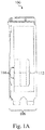
- FIG. 1A is a front side view of a circuit card assembly 100 defining the GPGPU unit.
- FIG. 1B is a side view of the circuit card assembly 100.
- a conventional design for a circuit card assembly 100 includes a substantially planar circuit card 102 with a front end 102A, a back end 102B, a first longitudinal edge 102C and a second longitudinal edge 102D.
- the longitudinal edges 102C and 102D are substantially parallel to each other.
- the circuit card 102 can also include at least one bus connector 104 extending from one of longitudinal edges 102C and 102D.
- a bus connector 104 extends from longitudinal edge 102D and substantially parallel to the plane of circuit card 102.
- the bus connector 104 in FIGs. 1A and 1B is illustrated as a Peripheral Component Interconnect Express (PCIe) bus, but the various embodiments are not limited in this regard. Rather, any other computer bus type can be used in the various embodiments without limitation.
- PCIe Peripheral Component Interconnect Express
- the circuit card 102 can be, for example, a printed circuit board (PCB) manufactured according to any known processes.
- PCB printed circuit board
- the various embodiments are not limited in this regard. Rather, any other technologies for forming a substrate or other substantially planar structure for mechanically supporting and electrically connecting various electronic components can be used in place of a PCB.
- the circuit card assembly 100 can also include a bracket structure 106 attached to the circuit card 102.
- the bracket structure 106 can include a bracket 108 configured for attachment to one or more bracket slots of a computer system to provide proper mechanical and electrical connection. The interplay between circuit cards and bracket slots is illustrated in FIG. 11 .
- FIG. 11 An exemplary computer system is illustrated in FIG. 11 .
- a computer system 1100 can include multiple bracket slots 1104 and bus connectors 1106.
- An add-on unit 1102, with a bus connector 1108 and a bracket 1110, is installed in the computer system 1100 by inserting the add-on unit 1102 into the computer system so that a bus connector 1108 engages with a corresponding bus connector 1106 of the computer system 1100.
- the bus connector 1106 may be on a motherboard or daughterboard of the computer system 1100.
- the bus connectors 1106 and 1108, the bracket 1110, and the bracket slots 1104 are all arranged so that proper insertion of the add-on unit 1102 into computer system 1100 results in: (1) the bus connectors 1106 and 1108 being aligned and connecting properly to each other; and (2) the bracket 1110 being aligned and engaging properly with the bracket slot 1104.
- the circuit card assembly 100 is configured to support I/O and GPGPU features by incorporating certain components.
- the circuit card 102 is configured to support two or more GPUs 110 and a connector assembly 112.
- the connector assembly 112 can include a number of I/O connectors 114.
- the circuit card assembly 100 can include additional components, such as switch elements 116, memory elements 118, and other controller elements 120.
- controller elements 120 can include a management controller or other controller types for managing various operations of the other components of the circuit card 102.
- a GPGPU unit is not limited to the components listed above, and may include more or less components than shown in FIGs. 1A and 1B .
- circuit card assembly 100 would provide a functional GPGPU-based I/O unit, there are various problems with the configuration shown in FIGs. 1A and 1B .
- bracket slots in the computer system consist of a series of openings at a fixed pitch. As such, if the arrangement of I/O connectors associated with the circuit card assembly is wider than the width of the slots, insertion is impossible.
- ISA Industry Standard Architecture
- circuit card assembly 100 is configured to have a bracket assembly 106 that is the width of two ISA bracket slots.
- the I/O connectors 114 do not line up with the ISA bracket slot arrangement.
- the circuit card assembly 100 would be incompatible with such a computer system.
- I/O connectors 114 could be configured to be compatible with a traditional ISA bracket slot arrangement, there are still concerns with such an arrangement.
- the introduction of I/O connectors can potentially introduce an additional heat source.
- the additional I/O connectors can ventilation through the add-on processing unit. In either case, this can lead to elevated temperatures in the add-on unit.
- some types of I/O components may be incompatible with the resulting high temperature environment.
- optical I/O components such as optical transceivers, tend to be more sensitive to temperature changes than other components. As a result, the performance of some types of I/O components may be adversely affected when incorporated into the add-on processing unit.
- the various embodiments are directed to new architectures for add-on processing units, such as GPGPU-based I/O units, that provide compatibility with computer systems having bracket slots with single or multiple openings and that address thermal issues associated with such add-on processing units.
- FIG. 2 shows a front view of a circuit card assembly 200 configured in accordance with an embodiment.
- the circuit card assembly 200 can be configured in a similar fashion as circuit card assembly 100 in FIGs. 1A and 1B .
- the circuit card assembly 200 can be configured so that any I/O connectors 214 extending through the bracket 208 of bracket structure 206 are aligned with bracket opening areas 204.
- the bracket opening areas 204 are designed according the desired bracket slot design, such as an ISA bracket slot design. In this manner, when circuit card assembly is inserted into a computer system, the I/O connectors 214 will align with the openings in the bracket slots of the computer system.
- FIG. 2 shows an arrangement of four connectors, but the various embodiments are not limited in this regard. That is, any number of connectors can be provided. However, in the various embodiments, the number of connectors should be limited so as not to extend across the entire length of a corresponding bracket structure. This configuration is needed so that ventilation openings 250 can be provided in a portion of the of the bracket structure 206, at least along bracket opening areas 204.
- FIG. 2 can be accomplished in a variety of ways. In particular, by providing a new connector assembly configuration. Exemplary configurations for connector assemblies in accordance with the various embodiments are illustrated in FIGs. 3, 4 , 5A, and 5B .
- FIG. 3 shows a cross-section view of a circuit card assembly 300 configured in accordance with an embodiment.
- FIG. 3 shows a cross-section view of the portion of the circuit card assembly 300 near a front end 302A of the circuit card 302.
- the circuit card assembly 300 can include components similar to the circuit card assembly 100 in FIGs. 1A and 1B .
- the circuit card assembly 300 can include a circuit card 302, a bracket structure 306 (including ventilation openings which are not shown for ease of illustration), GPU's 310, and a connector assembly 312 with a stacked arrangement of I/O connectors 314.
- circuit card assembly 300 can also include other components of the circuit card assembly 100, even if not explicitly described herein.
- the circuit card assembly 300 in FIG. 3 is configured to provide an arrangement of I/O connectors 314 corresponding to that illustrated in FIG. 2 . That is, the I/O connectors 314 extending through the bracket structure 306 are arranged so as to be aligned with bracket opening areas. As noted above with respect to FIG. 2 , this configuration is provided in FIG. 3 so that the I/O connectors 314 will align with the openings in the bracket slots of the computer system.
- FIG. 3 The configuration of FIG. 3 is accomplished by configuring the proper arrangement of I/O connectors 314 in a connector assembly 312 that is a unitary body. That is, a single component is mounted on circuit card 302 and houses supporting hardware and electronics for I/O connectors 314.
- FIG. 4 One exemplary configuration is shown in FIG. 4 .
- FIG. 4 there is shown a cross-section view of a circuit card assembly 400 configured in accordance with an embodiment, in particular, a cross-section view of the portion of the circuit card assembly 400 near a front end 402A of the circuit card 402.
- the circuit card assembly 400 can include components similar to the circuit card assembly 100 in FIGs. 1A and 1B .
- the circuit card assembly 400 can include a circuit card 402, a bracket structure 406 (including ventilation openings which are not shown for ease of illustration), GPU's 410, and a connector assembly 412 with I/O connectors 414.
- the operation of components 402, 406, 410, 412, and 414 is substantially similar to that of components 102, 106, 110, 112, and 114 in FIGs. 1A and 1B .
- the description components 102, 106, 110, 112, and 114 is sufficient for describing components 402, 406, 410, 412, and 414.
- circuit card assembly 400 can also include other components of the circuit card assembly 100, even if not explicitly described herein.
- the circuit card assembly 400 in FIG. 4 is also configured to provide an arrangement of I/O connectors 414 corresponding to that illustrated in FIG. 2 . That is, the I/O connectors 414 extending through bracket structure 406 are arranged so as to be aligned with bracket opening areas. As noted above with respect to FIG. 2 , this configuration is provided in FIG. 4 so that the I/O connectors 414 will align with the openings in the bracket slots of the computer system.
- a first body 413A is disposed directly on the circuit card 402.
- a second body 413B is attached to the circuit card 402, but is configured to extend over the first body 413A without contacting the first body 413A.
- the second body 413B can be mechanically supported via its connection to the circuit card 402 and the contact between a corresponding I/O connector 414 and the bracket structure 406.
- additional support structures can be provided to mechanically support the second body 413B.
- FIG. 5A Another alternative to a unitary body configuration is shown in FIGs. 5A and 5B .
- FIG. 5A there is shown a cross-section view of a circuit card assembly 500 configured in accordance with an embodiment.
- FIG. 5A shows a cross-section view of the portion of the circuit card assembly 500 near a front end 502A of the circuit card 502.
- FIG. 5B shows a side view of the circuit card assembly 500.
- the circuit card assembly 500 can include components similar to the circuit card assembly 100 in FIGs. 1A and 1B .
- the circuit card assembly 500 can include a circuit card 502, a bracket structure 506 (including ventilation openings which are not shown for ease of illustration), GPU's 510, and a connector assembly 512 with I/O connectors 514.
- the operation of components 502, 506, 510, 512, and 514 is substantially similar to that of components 102, 106, 110, 112, and 114 in FIGs. 1A and 1B .
- the description for components 102, 106, 110, 112, and 114 is sufficient for describing components 502, 506, 510, 512, and 514.
- circuit card assembly 500 can also include other components of the circuit card assembly 100, even if not explicitly described herein.
- the circuit card assembly 500 in FIGs. 5A and 5B is configured to provide an arrangement of I/O connectors 514 corresponding to that illustrated in FIG. 2 . That is, the I/O connectors 514 extending through bracket structure 506 are aligned with bracket opening areas. As noted above with respect to FIG. 2 , this configuration is provided in FIGs. 5A and 5B so that the I/O connectors 514 will align with the openings in the bracket slots of the computer system.
- FIGs. 5A and 5B this is accomplished by configuring the connector assembly 512 as two or more bodies, but using additional circuit cards.
- a first body 513A is disposed directly on the circuit card 502.
- a second body 513B is disposed directly on a circuit sub-board 550, which is shown in FIG. 5A as being attached to the circuit card 502 via a complementary pair of connectors 552 and 554.
- the circuit sub-board 550 is configured to extend over the first body 513A without contacting the first body 513A.
- the circuit sub-board 550 can be mechanically supported via the connectors 552 and 554 and the contact between a corresponding I/O connector 514 and the bracket structure 506.
- additional support structures can be provided to mechanically support the circuit sub-board 550.
- the connectors provide both the mechanical and electrical connections in circuit card assembly 500
- the various embodiments are not limited in this regard. Rather, the mechanical and electrical connections can be separate.
- mechanical support structure can be provided to position the circuit sub-board 550 in circuit card assembly 500.
- cable, connectors, and the like can be used to couple the circuit sub-board 550 to the circuit card 502 while providing little or no mechanical support.
- the various embodiments can incorporate any number of I/O connectors.
- the I/O connectors can be provided in various combinations.
- the unitary body connector assembly 312 can provide 2, 3, 4, or any number of I/O connectors.
- two or more side-by-side unitary bodies can be disposed on the circuit card to define the connector assembly.
- each unitary body can be a 2 x 1 (tall x wide) arrangement of connectors.
- a similar configuration can be utilized for the configurations shown in FIGs. 4 , 5A, and 5B . That is, referring now to FIG.
- the first body 413A and the second body 413B can be configured to provide 1, 2, or more connectors.
- the first body 413A and the second body 413B can be 1 x 2 arrangement of connectors.
- the first body 513A and the second body 513B can also be configured to provide 1, 2, or more connectors.
- FIGs. 3, 4 , 5A, and 5B illustrate exemplary configurations for implementing an arrangement of I/O connector compatible with an arrangement of bracket slots at a fixed pitch, there are still thermal challenges that need to be addressed.
- a typical add-on processing unit such as a GPGPU unit
- some types of add-on processing units typically do not include a fan or other cooling device.
- a fan or other cooling device typically included in the case of a GPGPU unit.
- such units are typically cooled by airflow generated by a fan in the computer system the GPGPU unit is installed in.
- fans are typically configured to supply air at the back end 102B and exit out the front end 102A.
- a first problem in such a configuration including additional components in the airflow path, such as I/O connectors, tend to block airflow. This results in even higher temperatures in the GPGPU unit.
- a second problem may then be exacerbated -- temperature sensitivity of the I/O connectors.
- the performance of certain optical transceivers used in many applications such as Quad Small Form-factor Pluggable (QSFP) transceivers, is susceptible to increased temperature.
- QSFP Quad Small Form-factor Pluggable
- the various embodiments are also directed to methods for providing improved cooling in an add-on processing unit incorporating these types of I/O connectors. Specifically, the various embodiments are directed to methods for improving cooling at least in the region of the connector assembly for the configurations discussed above.
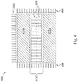
- FIG. 6 illustrates a cross-section view of a connector assembly 600 in accordance with an embodiment.
- the connector assembly 600 consists of a first body 613A, which would be disposed on a circuit card, and a second body 613B, which is disposed above the first body 613A, and a space 613C in between bodies 613A and 613B.
- Such bodies can be substantially similar to those illustrated in FIGs. 4 and 5A .
- the first body 613A and the second body 613B can be part of a unitary body, as shown in FIG. 3 . That is, the unitary body of FIG. 3 can be configured to include a space between connector portions.
- a first potential cooling method is to utilize a series of heat sinks.
- a number of heat sinks 602, 604, 606 can be attached to the outer surfaces of the connector assembly 600.
- heat sinks 608 can also be positioned in any spaces 613C defined in the connector assembly.
- conventional ventilation via computer system fans may be sufficient to keep the connector assembly 600 at an acceptable temperature.
- FIG. 6 appears to show fin-type heat sinks, this is solely for purposes of illustration. In the various embodiments, any other type of heat sink can be used without limitation.
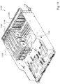
- FIG. 7 shows an isometric view of a circuit card assembly 700.
- the circuit card assembly 700 can be configured as described above with respect to any of FIGs. 2 , 3 , 4 , 5A, or 5B . That is, the circuit card assembly 700 in FIG. 7 can include a connector assembly 712 disposed on a circuit card 702. Additionally, the circuit card assembly 700 can include any of the components described above with respect to any of FIGs. 2 , 3 , 4 , 5A, or 5B .
- the connector assembly is illustrated as including a heat sink arrangement, as discussed above with respect to FIG. 6 . However, in other embodiments, the connector assembly 712 can be provided without the heat sink arrangement of FIG. 6 .
- the circuit card assembly 700 includes a cover 750 extending over the circuit card 702 from a first end 702A of the circuit card 702 to a second end 702B of the circuit card 702.
- the cover 750 is positioned to cover the components disposed on the circuit card 702.
- the cover 750 is configured to direct airflow through the circuit card assembly 700 from the back end 702B to the front end 702A.
- the cover 750 can be generally U-shaped so that the cover 750 extends from a first longitudinal edge 702C of the circuit card 702 to a second longitudinal edge 702D of the circuit card 702.
- the cover 750 surrounds any components disposed on circuit card 702 and channels air through these components.
- the cover 750 is configured to provide extra ventilation for the connector assembly 712.
- the cover 750 is configured to include an opening or cutout 752 that exposes all or some of the connector assembly 712.
- the connector assembly 712 can be exposed to cooler air outside of the cover 750, i.e., outside of the circuit card assembly 700. In this manner, the cooling of the connector assembly is not dependent on solely the airflow though the cover 750.
- FIG. 8 shows that
- FIG. 8 shows airflow with respect to circuit card assembly 700.
- the cover 750 results in a first airflow 802 through the circuit card assembly 700 under cover 750.
- a second external (and cooler) airflow 804 is provided for the connector assembly 712.
- the size of the cutout can vary. For example, even with the cutout 752, some heated air may still reach the connector assembly 712. Accordingly, in some embodiments, the distance between the edges of the cutout 752 and the connector assembly 712 can be increased so that at least some heated air escapes prior to reaching the connector assembly 712. Moreover, in other cases, the edges of the cutout 752 can be configured to reduce the amount of heated air inside the cover 750 reaching the connector assembly 712. For example, the edges of the cutout 752 can be rolled, angled, or otherwise shaped to re-direct some or all of the airflow within the cover 750 away from the connector assembly 712.
- FIG. 9 shows airflow (represented by arrows) over a circuit card assembly 900 under a cover, similar to the configuration described in FIGs. 7 and 8 , but with no cutout.
- substantial heating of the connector assembly 912 may occur.
- the airflow cools the GPUs 910 first, air reaching the area containing the connector assembly 912 will be heated.
- the connector assembly 912 may not be appropriately cooled. This problem can be addressed by the configuration in FIG. 10 .
- FIG. 10 shows airflow (represented by arrows) over a circuit card assembly 1000 under a cover, but with diverting features in accordance with an embodiment.
- the circuit card assembly 1000 can be divided into two airflow zones 1050 and 1052.
- a first zone 1050 can be established so that a connector assembly 1012 is at least partially isolated from airflow across the circuit card assembly 1000 associated with the GPUs 1010.
- a second zone 1052 can be establish so that the GPUs 1010 are at least partially isolated from airflow across the circuit card assembly 1000 associated with the connector assembly 1012. In this manner, each of the connector assembly 1012 and the GPUs 1010 receive fresh air independently.
- the cover can include walls extending downward.
- the cover can include a wall following the edge 1054 between the first zone 1050 and the second zone 1052.
- a circuit card 1002 can have an upward extending wall following edge 1054.
- a combination of upward extending wall features from the circuit card 1002 and downward extending wall features from the cover can define a wall following edge 1054.
Landscapes
- Engineering & Computer Science (AREA)
- Theoretical Computer Science (AREA)
- General Engineering & Computer Science (AREA)
- Computer Hardware Design (AREA)
- Physics & Mathematics (AREA)
- General Physics & Mathematics (AREA)
- Human Computer Interaction (AREA)
- Power Engineering (AREA)
- Microelectronics & Electronic Packaging (AREA)
- Cooling Or The Like Of Electrical Apparatus (AREA)
- Mounting Of Printed Circuit Boards And The Like (AREA)
Abstract
Description
- The present invention relates to add-on processing units, and more specifically to apparatus and methods for assembling add-on units with input/output connectors.
- In recent years, add-on processing units, such as general-purpose computing on graphics processing units (GPGPU or GP2U), have become popular. In a GPGPU unit, a graphics processing unit (GPU), which typically handles computation only for computer graphics, is configured to perform computation in applications traditionally handled by the central processing unit (CPU). In operation, a GPGPU unit analyzes data from the CPU as if it were in image or other graphic form. Further, although GPUs operate at lower frequencies than CPUs, they typically have many times the number of cores. Thus, GPUs can operate on pictures and graphical data at far faster rates than traditional CPUs. Consequently, migrating data into graphical form, and then using the GPU to scan and analyze it, can result in significant improvements in computation time.
- More recently, GPGPU units have been investigated for improve throughput in communications applications. For example, a GPGPU unit can be configured to perform communications and signal processing functions at a much higher throughput or data rate that a traditional CPU. Thus, a GPGPU unit can significantly improve throughput in many types of transceiver systems.
- However, while a GPGPU unit may offer computational advantages, implementing a communications GPGPU unit is far from trivial. For one, traditional GPGPU unit design does not typically include input/output (I/O) ports that would be necessary for a communications-based GPGPU unit to operate efficiently. Second, the high performance of GPGPU unit comes at a high thermal cost, resulting in most GPGPU units running at relatively high temperatures (typically 80°C-85°C). As a result, these high temperatures do not provide an adequate environment for communication of certain types of signals (e.g., optical signals). Finally, GPGPU unit designs incorporating I/O ports typically require specialized connection and mounting schemes, thereby providing limited backward compatibility with older chassis support traditional form factor designs for add-on cards.
- Therefore, there is a need for add-on processing unit designs, including I/O connectors that consider thermal issues and backward compatibility issues.
- Particular and preferred aspects of the present invention are set out in the accompanying independent and dependent claims. Features of the dependent claims may be combined with features of the independent claims as appropriate, and in combinations other than those explicitly set out in the claims.
- Embodiments concern a circuit card assembly defining an add-on processing unit with I/O connectors. A circuit card assembly according to a first embodiment is configured for removable attachment to a computer system having a plurality of bracket slots arranged with a fixed pitch. The circuit card assembly includes a circuit card having a front end, a back end, and substantially parallel longitudinal edges between the front end and the back end. The circuit card includes at least one bus connector extending from one of the longitudinal edges. The circuit card assembly also includes a bracket structure that provides a mounting surface at the front end of said circuit card. The mounting surface extends perpendicularly to a first surface of said circuit card and extends perpendicularly to said longitudinal edges. The mounting surface comprises a bracket for engaging with a plurality of adjacent ones of the plurality of bracket slots. The circuit card assembly also includes a connector assembly disposed on the first surface of said circuit card at said front end.
- The connector assembly includes a first input/output (I/O) connector and a second I/O connector in a stacked arrangement with respect to the first surface of said circuit card. A width of the connector assembly is less than a width of the circuit card between the longitudinal edges. The first I/O connector is positioned between the second I/O connector and the circuit card. Further, the first I/O connector and the second I/O connector extend through the bracket and are separated by the fixed pitch.
- In some implementations, the connector assembly comprises a unitary body mechanically coupling the first I/O connector and the second I/O connector. Further, the connector assembly can further include one or more heat sink structures disposed on the outer surface of the unitary body. The unitary body can also include one or more spaces between the first I/O connector and the second I/O connector. The connector assembly can include one or more additional heat sink structures disposed in at least one of the spaces. The additional heat sink structures can be a plurality of fins extending parallel to the longitudinal edges.
- In some implementations, the connector assembly includes a first connector structure, extending from the first surface of the circuit card and containing the first I/O connector. The connector assembly also includes a second connector structure, extending from the first surface of the circuit card independently from the first connector structure, and containing the second I/O connector. The second connector structure can include a circuit sub-board, having the second I/O connector disposed thereon, and a board connector structure coupling the circuit sub-board to the circuit card.
- In some implementations, the circuit card assembly can include a U-shaped cover disposed over the first surface of the circuit card. The U-shaped cover can have a cut-out for a portion of the first surface of the circuit card having the connector assembly disposed thereon.
- In some implementations, the circuit card assembly can also include a plurality of heat generating components disposed on the first surface of the circuit card. These heat generating components can be one or more graphics processing units.
- In some implementations, the U-shaped cover has a first open end coincident with the front end of the circuit card and a second open end coincident with the back end of the circuit card. The U-shaped cover can also include and a wall extending from an inner surface of the U-shaped cover towards the first surface of the circuit card. The wall can define at least a first zone and a second zone in the circuit card assembly. The first zone defines a path from the first open end to the second open end and includes the connector assembly, but excludes the plurality of heat generating components. The second zone defines a path from the first open end to the second open end and includes the plurality of heat generating components, but excludes the connector assembly.
- In some implementations, the bus connector is a Peripheral Component Interconnect Express (PCIe) connector. Further, each of the first I/O connector and the second I/O connector can be Quad Small Form-factor Pluggable (QSFP) connectors. Additionally, the plurality of bracket slots can be ISA bracket slots.
- In some implementations, the connector assembly can further include a third I/O connector and a fourth I/O connector, in a stacked arrangement with respect to the first surface of the circuit card.
- The present invention will be described further, by way of example only, with reference to preferred embodiments thereof as illustrated in the accompanying drawings, in which:
-
FIG. 1A is a front side view of a conventional circuit card assembly that is useful for describing the various embodiments. -
FIG. 1B is a side view of the circuit card assembly ofFIG. 1A . -
FIG. 2 shows a front view of a circuit card assembly configured in accordance with an embodiment. -
FIG. 3 shows a cross-section view of a portion of circuit card assembly configured in accordance with an embodiment. -
FIG. 4 shows a cross-section view of a portion of circuit card assembly configured in accordance with an embodiment. -
FIG. 5A shows a cross-section view of a portion of circuit card assembly configured in accordance with an embodiment. -
FIG. 5B shows a side view of the circuit card assembly ofFIG. 5A . -
FIG. 6 illustrates a cross-section view of a connector assembly in accordance with an embodiment. -
FIG. 7 shows an isometric view of a circuit card assembly configured in accordance with an embodiment. -
FIG. 8 shows airflow with respect to the circuit card assembly ofFIG. 7 . -
FIG. 9 shows airflow over a circuit card assembly under a cover that is useful for describing the various embodiments. -
FIG. 10 shows airflow over a circuit card assembly under a cover and including diverting features in accordance with an embodiment. -
FIG. 11 shows an exemplary computer system that is useful for describing the various embodiments. - The present invention is described with reference to the attached figures, wherein like reference numerals are used throughout the figures to designate similar or equivalent elements. The figures are not drawn to scale, and they are provided merely to illustrate the instant invention. Several aspects of the invention are described below with reference to example applications for illustration. It should be understood that numerous specific details, relationships, and methods are set forth to provide a full understanding of the invention. One having ordinary skill in the relevant art, however, will readily recognize that the invention can be practiced without one or more of the specific details or with other methods. In other instances, well-known structures or operations are not shown in detail to avoid obscuring the invention. The present invention is not limited by the illustrated ordering of acts or events, as some acts may occur in different orders and/or concurrently with other acts or events. Furthermore, not all illustrated acts or events are required to implement a methodology in accordance with the present invention.
- As discussed above, inclusion of I/O ports in an add-on processing unit, such as a GPGPU unit, is not a trivial modification. As further noted above, there concerns regarding backward compatibility and operating temperatures. These are discussed in more detail below with respect to
FIGs. 1A and1B . - Although the various embodiments will be discussed primarily with respect to a GPGPU unit, this is solely for ease of illustration. The methods discussed herein can be applied to any other type of add-on processing unit. For example, an FPGA HPC card or an Ethernet switch card.
- A conventional design for adding I/O ports to a
circuit card assembly 100 of an add-on processing unit, specifically a GPGPU unit, is illustrated inFIGs. 1A and1B .FIG. 1A is a front side view of acircuit card assembly 100 defining the GPGPU unit.FIG. 1B is a side view of thecircuit card assembly 100. - As shown in
FIGs. 1A and1B , a conventional design for acircuit card assembly 100 includes a substantiallyplanar circuit card 102 with afront end 102A, aback end 102B, a firstlongitudinal edge 102C and a secondlongitudinal edge 102D. In thecircuit card assembly 100, thelongitudinal edges circuit card 102 can also include at least onebus connector 104 extending from one oflongitudinal edges FIG. 1A and1B , abus connector 104 extends fromlongitudinal edge 102D and substantially parallel to the plane ofcircuit card 102. Thebus connector 104 inFIGs. 1A and1B is illustrated as a Peripheral Component Interconnect Express (PCIe) bus, but the various embodiments are not limited in this regard. Rather, any other computer bus type can be used in the various embodiments without limitation. - The
circuit card 102 can be, for example, a printed circuit board (PCB) manufactured according to any known processes. However, the various embodiments are not limited in this regard. Rather, any other technologies for forming a substrate or other substantially planar structure for mechanically supporting and electrically connecting various electronic components can be used in place of a PCB. - The
circuit card assembly 100 can also include abracket structure 106 attached to thecircuit card 102. Thebracket structure 106 can include abracket 108 configured for attachment to one or more bracket slots of a computer system to provide proper mechanical and electrical connection. The interplay between circuit cards and bracket slots is illustrated inFIG. 11 . - An exemplary computer system is illustrated in
FIG. 11 . As shown inFIG. 11 , acomputer system 1100 can includemultiple bracket slots 1104 andbus connectors 1106. An add-onunit 1102, with abus connector 1108 and abracket 1110, is installed in thecomputer system 1100 by inserting the add-onunit 1102 into the computer system so that abus connector 1108 engages with a correspondingbus connector 1106 of thecomputer system 1100. Thebus connector 1106 may be on a motherboard or daughterboard of thecomputer system 1100. Thebus connectors bracket 1110, and thebracket slots 1104 are all arranged so that proper insertion of the add-onunit 1102 intocomputer system 1100 results in: (1) thebus connectors bracket 1110 being aligned and engaging properly with thebracket slot 1104. - Referring back to
FIGs. 1A and1B , thecircuit card assembly 100 is configured to support I/O and GPGPU features by incorporating certain components. For example, as shown inFIG. 1A , thecircuit card 102 is configured to support two ormore GPUs 110 and aconnector assembly 112. Theconnector assembly 112 can include a number of I/O connectors 114. In addition, thecircuit card assembly 100 can include additional components, such asswitch elements 116,memory elements 118, andother controller elements 120. For example,controller elements 120 can include a management controller or other controller types for managing various operations of the other components of thecircuit card 102. However, a GPGPU unit is not limited to the components listed above, and may include more or less components than shown inFIGs. 1A and1B . - Although the
circuit card assembly 100 would provide a functional GPGPU-based I/O unit, there are various problems with the configuration shown inFIGs. 1A and1B . - First, conventional connector assemblies are typically incompatible with conventional bracket slot arrangements in conventional computer systems. For example, many computer systems typically utilize an Industry Standard Architecture (ISA) slot configuration for mechanically coupling add-on units to a computer system, even to support PCIe components. In this type of configuration, the bracket slots in the computer system consist of a series of openings at a fixed pitch. As such, if the arrangement of I/O connectors associated with the circuit card assembly is wider than the width of the slots, insertion is impossible.
- This is the case with
circuit card assembly 100. As shown inFIG. 1A ,circuit card assembly 100 is configured to have abracket assembly 106 that is the width of two ISA bracket slots. However, the I/O connectors 114 do not line up with the ISA bracket slot arrangement. As a result, if the ISA bracket slots of the computer system consist of a series of openings as opposed to a completely open space, thecircuit card assembly 100 would be incompatible with such a computer system. - Second, even if the arrangement of the I/
O connectors 114 could be configured to be compatible with a traditional ISA bracket slot arrangement, there are still concerns with such an arrangement. In particular, the introduction of I/O connectors can potentially introduce an additional heat source. At the very least, the additional I/O connectors can ventilation through the add-on processing unit. In either case, this can lead to elevated temperatures in the add-on unit. Further, some types of I/O components may be incompatible with the resulting high temperature environment. For example, optical I/O components, such as optical transceivers, tend to be more sensitive to temperature changes than other components. As a result, the performance of some types of I/O components may be adversely affected when incorporated into the add-on processing unit. - In view of the foregoing issues, the various embodiments are directed to new architectures for add-on processing units, such as GPGPU-based I/O units, that provide compatibility with computer systems having bracket slots with single or multiple openings and that address thermal issues associated with such add-on processing units.
- First, as to providing compatibility, an add-on processing unit can be configured as shown in
FIG. 2. FIG. 2 shows a front view of acircuit card assembly 200 configured in accordance with an embodiment. Thecircuit card assembly 200 can be configured in a similar fashion ascircuit card assembly 100 inFIGs. 1A and1B . However, as shown inFIG. 2 , thecircuit card assembly 200 can be configured so that any I/O connectors 214 extending through thebracket 208 ofbracket structure 206 are aligned withbracket opening areas 204. Thebracket opening areas 204 are designed according the desired bracket slot design, such as an ISA bracket slot design. In this manner, when circuit card assembly is inserted into a computer system, the I/O connectors 214 will align with the openings in the bracket slots of the computer system. - The exemplary configuration shown in
FIG. 2 shows an arrangement of four connectors, but the various embodiments are not limited in this regard. That is, any number of connectors can be provided. However, in the various embodiments, the number of connectors should be limited so as not to extend across the entire length of a corresponding bracket structure. This configuration is needed so thatventilation openings 250 can be provided in a portion of the of thebracket structure 206, at least alongbracket opening areas 204. - The configuration shown in
FIG. 2 can be accomplished in a variety of ways. In particular, by providing a new connector assembly configuration. Exemplary configurations for connector assemblies in accordance with the various embodiments are illustrated inFIGs. 3, 4 ,5A, and 5B . -
FIG. 3 shows a cross-section view of acircuit card assembly 300 configured in accordance with an embodiment. In particular,FIG. 3 shows a cross-section view of the portion of thecircuit card assembly 300 near afront end 302A of thecircuit card 302. As shown inFIG. 3 , thecircuit card assembly 300 can include components similar to thecircuit card assembly 100 inFIGs. 1A and1B . For example, thecircuit card assembly 300 can include acircuit card 302, a bracket structure 306 (including ventilation openings which are not shown for ease of illustration), GPU's 310, and aconnector assembly 312 with a stacked arrangement of I/O connectors 314. The operation ofcomponents components FIGs. 1A and1B . Thus, the description forcomponents components circuit card assembly 300 can also include other components of thecircuit card assembly 100, even if not explicitly described herein. - However, unlike the
circuit card assembly 100 inFIGs. 1A and1B , thecircuit card assembly 300 inFIG. 3 is configured to provide an arrangement of I/O connectors 314 corresponding to that illustrated inFIG. 2 . That is, the I/O connectors 314 extending through thebracket structure 306 are arranged so as to be aligned with bracket opening areas. As noted above with respect toFIG. 2 , this configuration is provided inFIG. 3 so that the I/O connectors 314 will align with the openings in the bracket slots of the computer system. - The configuration of
FIG. 3 is accomplished by configuring the proper arrangement of I/O connectors 314 in aconnector assembly 312 that is a unitary body. That is, a single component is mounted oncircuit card 302 and houses supporting hardware and electronics for I/O connectors 314. - However, the various embodiments are not limited to unitary body configurations. Rather, connectors can be supporting while using multiple bodies mounted with a circuit card assembly. One exemplary configuration is shown in
FIG. 4 . InFIG. 4 , there is shown a cross-section view of a circuit card assembly 400 configured in accordance with an embodiment, in particular, a cross-section view of the portion of the circuit card assembly 400 near afront end 402A of thecircuit card 402. As shown inFIG. 4 , the circuit card assembly 400 can include components similar to thecircuit card assembly 100 inFIGs. 1A and1B . For example, the circuit card assembly 400 can include acircuit card 402, a bracket structure 406 (including ventilation openings which are not shown for ease of illustration), GPU's 410, and aconnector assembly 412 with I/O connectors 414. The operation ofcomponents components FIGs. 1A and1B . Thus, thedescription components components circuit card assembly 100, even if not explicitly described herein. - However, unlike the
circuit card assembly 100 inFIGs. 1A and1B , the circuit card assembly 400 inFIG. 4 is also configured to provide an arrangement of I/O connectors 414 corresponding to that illustrated inFIG. 2 . That is, the I/O connectors 414 extending throughbracket structure 406 are arranged so as to be aligned with bracket opening areas. As noted above with respect toFIG. 2 , this configuration is provided inFIG. 4 so that the I/O connectors 414 will align with the openings in the bracket slots of the computer system. - In the configuration of
FIG. 4 , this is accomplished by configuring theconnector assembly 412 as two or more bodies, each separately coupled to thecircuit card 402. For example, as shown inFIG. 4 , afirst body 413A is disposed directly on thecircuit card 402. Asecond body 413B is attached to thecircuit card 402, but is configured to extend over thefirst body 413A without contacting thefirst body 413A. - The
second body 413B can be mechanically supported via its connection to thecircuit card 402 and the contact between a corresponding I/O connector 414 and thebracket structure 406. However, in some configurations, additional support structures can be provided to mechanically support thesecond body 413B. - Another alternative to a unitary body configuration is shown in
FIGs. 5A and 5B . InFIG. 5A , there is shown a cross-section view of acircuit card assembly 500 configured in accordance with an embodiment. In particular,FIG. 5A shows a cross-section view of the portion of thecircuit card assembly 500 near afront end 502A of thecircuit card 502.FIG. 5B shows a side view of thecircuit card assembly 500. As shown inFIGs. 5A and 5B , thecircuit card assembly 500 can include components similar to thecircuit card assembly 100 inFIGs. 1A and1B . For example, thecircuit card assembly 500 can include acircuit card 502, a bracket structure 506 (including ventilation openings which are not shown for ease of illustration), GPU's 510, and aconnector assembly 512 with I/O connectors 514. The operation ofcomponents components FIGs. 1A and1B . Thus, the description forcomponents components circuit card assembly 500 can also include other components of thecircuit card assembly 100, even if not explicitly described herein. - However, unlike the
circuit card assembly 100 inFIGs. 1A and1B , thecircuit card assembly 500 inFIGs. 5A and 5B is configured to provide an arrangement of I/O connectors 514 corresponding to that illustrated inFIG. 2 . That is, the I/O connectors 514 extending throughbracket structure 506 are aligned with bracket opening areas. As noted above with respect toFIG. 2 , this configuration is provided inFIGs. 5A and 5B so that the I/O connectors 514 will align with the openings in the bracket slots of the computer system. - In the configuration of
FIGs. 5A and 5B , this is accomplished by configuring theconnector assembly 512 as two or more bodies, but using additional circuit cards. For example, as shown inFIGs. 5A and 5B , afirst body 513A is disposed directly on thecircuit card 502. Asecond body 513B is disposed directly on acircuit sub-board 550, which is shown inFIG. 5A as being attached to thecircuit card 502 via a complementary pair ofconnectors - The
circuit sub-board 550 is configured to extend over thefirst body 513A without contacting thefirst body 513A. The circuit sub-board 550 can be mechanically supported via theconnectors O connector 514 and thebracket structure 506. However, in some configurations, additional support structures can be provided to mechanically support thecircuit sub-board 550. - Moreover, although the connectors provide both the mechanical and electrical connections in
circuit card assembly 500, the various embodiments are not limited in this regard. Rather, the mechanical and electrical connections can be separate. For example, mechanical support structure can be provided to position thecircuit sub-board 550 incircuit card assembly 500. Separately, cable, connectors, and the like can be used to couple thecircuit sub-board 550 to thecircuit card 502 while providing little or no mechanical support. - As noted above, the various embodiments can incorporate any number of I/O connectors. Furthermore, the I/O connectors can be provided in various combinations. For example, referring back to
FIG. 3 , the unitarybody connector assembly 312 can provide 2, 3, 4, or any number of I/O connectors. In some cases, instead of a single unitary body connector assembly, two or more side-by-side unitary bodies can be disposed on the circuit card to define the connector assembly. In such a configuration, each unitary body can be a 2 x 1 (tall x wide) arrangement of connectors. A similar configuration can be utilized for the configurations shown inFIGs. 4 ,5A, and 5B . That is, referring now toFIG. 4 , thefirst body 413A and thesecond body 413B can be configured to provide 1, 2, or more connectors. For example, thefirst body 413A and thesecond body 413B can be 1 x 2 arrangement of connectors. Similarly, referring toFIG. 5A , thefirst body 513A and thesecond body 513B can also be configured to provide 1, 2, or more connectors. - While
FIGs. 3, 4 ,5A, and 5B illustrate exemplary configurations for implementing an arrangement of I/O connector compatible with an arrangement of bracket slots at a fixed pitch, there are still thermal challenges that need to be addressed. - As noted above, the processing components of a typical add-on processing unit, such as a GPGPU unit, generate a substantial amount of heat. Further, for cooling purposes, some types of add-on processing units, such as a GPGPU unit, typically do not include a fan or other cooling device. For example, in the case of a GPGPU unit, such units are typically cooled by airflow generated by a fan in the computer system the GPGPU unit is installed in. Referring to
FIG. 1B , fans are typically configured to supply air at theback end 102B and exit out thefront end 102A. - As expected, a first problem in such a configuration, including additional components in the airflow path, such as I/O connectors, tend to block airflow. This results in even higher temperatures in the GPGPU unit. A second problem may then be exacerbated -- temperature sensitivity of the I/O connectors. For example, the performance of certain optical transceivers used in many applications, such as Quad Small Form-factor Pluggable (QSFP) transceivers, is susceptible to increased temperature. As such, the various embodiments are also directed to methods for providing improved cooling in an add-on processing unit incorporating these types of I/O connectors. Specifically, the various embodiments are directed to methods for improving cooling at least in the region of the connector assembly for the configurations discussed above.
- A first cooling option is shown in
FIG. 6. FIG. 6 illustrates a cross-section view of aconnector assembly 600 in accordance with an embodiment. In the configuration ofFIG. 6 , theconnector assembly 600 consists of afirst body 613A, which would be disposed on a circuit card, and asecond body 613B, which is disposed above thefirst body 613A, and aspace 613C in betweenbodies FIGs. 4 and5A . Alternatively, thefirst body 613A and thesecond body 613B can be part of a unitary body, as shown inFIG. 3 . That is, the unitary body ofFIG. 3 can be configured to include a space between connector portions. - Regardless of the configuration, a first potential cooling method is to utilize a series of heat sinks. In particular, as shown in
FIG. 6 , a number ofheat sinks connector assembly 600. Additionally, as also shown inFIG. 6 ,heat sinks 608 can also be positioned in anyspaces 613C defined in the connector assembly. Thus, even in the elevated temperature environment of a GPGPU unit, an efficient means for drawing heat from theconnector assembly 600 is provided. Thus, conventional ventilation (via computer system fans) may be sufficient to keep theconnector assembly 600 at an acceptable temperature. - Although
FIG. 6 appears to show fin-type heat sinks, this is solely for purposes of illustration. In the various embodiments, any other type of heat sink can be used without limitation. - A second cooling option is shown in
FIG. 7. FIG. 7 shows an isometric view of acircuit card assembly 700. Thecircuit card assembly 700 can be configured as described above with respect to any ofFIGs. 2 ,3 ,4 ,5A, or 5B . That is, thecircuit card assembly 700 inFIG. 7 can include aconnector assembly 712 disposed on acircuit card 702. Additionally, thecircuit card assembly 700 can include any of the components described above with respect to any ofFIGs. 2 ,3 ,4 ,5A, or 5B . In the configuration illustrated inFIG. 7 , the connector assembly is illustrated as including a heat sink arrangement, as discussed above with respect toFIG. 6 . However, in other embodiments, theconnector assembly 712 can be provided without the heat sink arrangement ofFIG. 6 . - As shown in
FIG. 7 , thecircuit card assembly 700 includes acover 750 extending over thecircuit card 702 from afirst end 702A of thecircuit card 702 to asecond end 702B of thecircuit card 702. Thecover 750 is positioned to cover the components disposed on thecircuit card 702. Additionally, thecover 750 is configured to direct airflow through thecircuit card assembly 700 from theback end 702B to thefront end 702A. Thus, thecover 750 can be generally U-shaped so that thecover 750 extends from a firstlongitudinal edge 702C of thecircuit card 702 to a secondlongitudinal edge 702D of thecircuit card 702. Thus, thecover 750 surrounds any components disposed oncircuit card 702 and channels air through these components. - However, a potential issue with a cover in an add-on unit, such as GPGPU unit, is that the cover may trap heated air and thus direct that heated air to more sensitive components, such as I/O connectors in the connector assembly. Accordingly, as shown in
FIG. 7 , thecover 750 is configured to provide extra ventilation for theconnector assembly 712. In particular, thecover 750 is configured to include an opening orcutout 752 that exposes all or some of theconnector assembly 712. In this way, theconnector assembly 712 can be exposed to cooler air outside of thecover 750, i.e., outside of thecircuit card assembly 700. In this manner, the cooling of the connector assembly is not dependent on solely the airflow though thecover 750. For example, as shown inFIG. 8 . -
FIG. 8 shows airflow with respect tocircuit card assembly 700. As shown inFIG. 8 , thecover 750 results in afirst airflow 802 through thecircuit card assembly 700 undercover 750. However, by adding thecutout 752, a second external (and cooler)airflow 804 is provided for theconnector assembly 712. - In some cases, the size of the cutout can vary. For example, even with the
cutout 752, some heated air may still reach theconnector assembly 712. Accordingly, in some embodiments, the distance between the edges of thecutout 752 and theconnector assembly 712 can be increased so that at least some heated air escapes prior to reaching theconnector assembly 712. Moreover, in other cases, the edges of thecutout 752 can be configured to reduce the amount of heated air inside thecover 750 reaching theconnector assembly 712. For example, the edges of thecutout 752 can be rolled, angled, or otherwise shaped to re-direct some or all of the airflow within thecover 750 away from theconnector assembly 712. - A third cooling option is described with respect to
FIGs. 9 and 10. FIG. 9 shows airflow (represented by arrows) over acircuit card assembly 900 under a cover, similar to the configuration described inFIGs. 7 and 8 , but with no cutout. In such a configuration, substantial heating of theconnector assembly 912 may occur. In particular, since the airflow cools theGPUs 910 first, air reaching the area containing theconnector assembly 912 will be heated. Thus, theconnector assembly 912 may not be appropriately cooled. This problem can be addressed by the configuration inFIG. 10 . -
FIG. 10 shows airflow (represented by arrows) over acircuit card assembly 1000 under a cover, but with diverting features in accordance with an embodiment. As shown inFIG. 10 , thecircuit card assembly 1000 can be divided into twoairflow zones first zone 1050 can be established so that aconnector assembly 1012 is at least partially isolated from airflow across thecircuit card assembly 1000 associated with theGPUs 1010. Asecond zone 1052 can be establish so that theGPUs 1010 are at least partially isolated from airflow across thecircuit card assembly 1000 associated with theconnector assembly 1012. In this manner, each of theconnector assembly 1012 and theGPUs 1010 receive fresh air independently. - This configuration can be accomplished in a variety of ways. In one configuration, the cover can include walls extending downward. For example, the cover can include a wall following the
edge 1054 between thefirst zone 1050 and thesecond zone 1052. In another configuration, acircuit card 1002 can have an upward extendingwall following edge 1054. In still another configuration, a combination of upward extending wall features from thecircuit card 1002 and downward extending wall features from the cover can define awall following edge 1054. - The terminology used herein is for the purpose of describing particular embodiments only and is not intended to be limiting. As used herein, the singular forms "a", "an", and "the" are intended to include the plural forms as well, unless the context clearly indicates otherwise. Furthermore, to the extent that the terms "including", "includes", "having", "has", "with", or variants thereof are used in either the detailed description and/or the claims, such terms are intended to be inclusive in a manner similar to the term "comprising."
- Unless otherwise defined, all terms (including technical and scientific terms) used herein have the same meaning as commonly understood by one of ordinary skill in the art to which this invention belongs. It will be further understood that terms, such as those defined in commonly used dictionaries, should be interpreted as having a meaning that is consistent with their meaning in the context of the relevant art, and will not be interpreted in an idealized or overly formal sense unless expressly so defined herein.
- Although particular embodiments have been described herein, it will be appreciated that the invention is not limited thereto and that many modifications and additions thereto may be made within the scope of the invention. For example, various combinations of the features of the following dependent claims can be made with the features of the independent claims without departing from the scope of the present invention.
Claims (14)
- A circuit card assembly for removable attachment to a computer system (1100) having a plurality of bracket slots (1104) arranged with a fixed pitch, the circuit card assembly characterized by comprising:a circuit card (102) having a front end (102A), a back end (102B), and substantially parallel longitudinal edges (102C, 102D) between the front end (102A) and the back end (102B), the circuit card (102) including at least one bus connector (104) extending from one of the longitudinal edges (102C, 102D);a bracket structure (206) providing a mounting surface at the front end (102A) of the circuit card (102) extending perpendicularly to a first surface of the circuit card and extending perpendicularly to the longitudinal edges (102C, 102D), the mounting surface comprising a bracket (208) for engaging with a plurality of adjacent ones of the plurality of bracket slots (1104); anda connector assembly disposed on the first surface of the circuit card (102) at the front end (102A), the connector assembly comprising a first input/output (I/O) connector (214) and a second I/O connector (214) in a stacked arrangement with respect to the first surface of the circuit card (102), wherein a width of the connector assembly is less than a width of the circuit card (102) between the longitudinal edges (102C, 102D),wherein the first I/O connector (214) is positioned between the second I/O connector (214) and the circuit card (102), and wherein the first I/O connector (214) and the second I/O connector (214) extend through the bracket (208) and are separated by the fixed pitch.
- The circuit card assembly of claim 1, characterized in that the connector assembly (312) comprises a unitary body mechanically coupling the first I/O connector (314) and the second I/O connector (314).
- The circuit card assembly of claim 2, characterized in that the connector assembly (600) further comprises one or more heat sink structures (602, 604, 606) disposed on an outer surface of the unitary body.
- The circuit card assembly of claim 2 or claim 3, characterized in that the unitary body comprises one or more spaces (613C) between the first I/O connector and the second I/O connector, and wherein the connector assembly further comprises one or more additional heat sink structures (608) disposed in at least one of the spaces (613C).
- The circuit card assembly of claim 4, characterized in that the one or more additional heat sink structures (608) comprise a plurality of fins extending parallel to the longitudinal edges.
- The circuit card assembly of claim 1, characterized in that the connector assembly (412) comprises a first connector structure (413A) extending from the first surface of the circuit card (402) and containing the first I/O connector (414), and a second connector structure (413B) extending from the first surface of the circuit card (402) independently from the first connector structure (413A) and containing the second I/O connector (414).
- The circuit card assembly of claim 6, characterized in that the second connector structure comprises:a circuit sub-board (550) having the second I/O connector (514) disposed thereon; anda board connector structure (552, 554) coupling the circuit sub-board (550) to the circuit card (502).
- The circuit card assembly of any preceding claim, characterized by further comprising a U-shaped cover (750) disposed over the first surface of the circuit card (702), the U-shaped cover (750) having a cut-out (752) for a portion of the first surface of the circuit card (702) having the connector assembly (712) disposed thereon.
- The circuit card assembly of any of claims 1-7, characterized by further comprising:a plurality of heat generating components (1010) disposed on the first surface of the circuit card (1002); anda U-shaped cover (750) disposed over the first surface of the circuit card (1002), the U-shaped cover (750) having a first open end coincident with the front end (702A) of the circuit card (1002), a second open end coincident with the back end (702B) of the circuit card (1002), and a wall extending from an inner surface of the U-shaped cover (750) towards the first surface of the circuit card (1002), the wall defining at least a first zone (1050) and a second zone (1052),wherein the first zone (1050) defines a path from the first open end to the second open end including the connector assembly (1012) and excluding the plurality of heat generating components (1010), wherein the second zone (1052) defines a path from the first open end to the second open end excluding the connector assembly (1012) and including the plurality of heat generating components (1010).
- The circuit card assembly of claim 9, characterized in that the plurality of heat generating components (1010) comprise at least one graphics processing unit.
- The circuit card assembly of any preceding claim, characterized in that the bus connector (104) is a Peripheral Component Interconnect Express (PCIe) connector.
- The circuit card assembly of any preceding claim, characterized in that each of the first I/O connector (214) and the second I/O connector (214) are Quad Small Form-factor Pluggable (QSFP) connectors.
- The circuit card assembly of any preceding claim, characterized in that the plurality of bracket slots (1104) are ISA bracket slots.
- The circuit card assembly of any preceding claim, characterized in that the connector assembly further comprises a third I/O connector (214) and a fourth I/O connector (214) in a stacked arrangement with respect to the first surface of the circuit card (102).
Applications Claiming Priority (2)
| Application Number | Priority Date | Filing Date | Title |
|---|---|---|---|
| US201762535488P | 2017-07-21 | 2017-07-21 | |
| US15/886,409 US10381761B2 (en) | 2017-07-21 | 2018-02-01 | Add-on processing unit with I/O connectors |
Publications (2)
| Publication Number | Publication Date |
|---|---|
| EP3432118A1 true EP3432118A1 (en) | 2019-01-23 |
| EP3432118B1 EP3432118B1 (en) | 2020-11-25 |
Family
ID=62495610
Family Applications (1)
| Application Number | Title | Priority Date | Filing Date |
|---|---|---|---|
| EP18175327.8A Active EP3432118B1 (en) | 2017-07-21 | 2018-05-31 | Add-on processing unit with i/o connectors |
Country Status (5)
| Country | Link |
|---|---|
| US (1) | US10381761B2 (en) |
| EP (1) | EP3432118B1 (en) |
| JP (1) | JP6630784B2 (en) |
| CN (1) | CN109283974B (en) |
| TW (1) | TWI665546B (en) |
Families Citing this family (4)
| Publication number | Priority date | Publication date | Assignee | Title |
|---|---|---|---|---|
| US11442498B2 (en) * | 2019-08-02 | 2022-09-13 | Smart Embedded Computing, Inc. | Universal bracket for multiple form factors of PCIe cards in OCP sled environments |
| US11406036B2 (en) * | 2019-11-13 | 2022-08-02 | Hewlett Packard Enterprise Development Lp | Flexible I/O server interface card orientation |
| US11737232B2 (en) * | 2021-09-20 | 2023-08-22 | Dell Products L.P. | Universal bracket for peripheral devices |
| US12167577B2 (en) * | 2022-06-06 | 2024-12-10 | Arista Networks, Inc. | Pluggable module and cage for improving airflow in network switch system |
Citations (3)
| Publication number | Priority date | Publication date | Assignee | Title |
|---|---|---|---|---|
| US20040145879A1 (en) * | 2003-01-23 | 2004-07-29 | Hensley James D. | Multi-slot CompactPCI blade assembly |
| US20060044774A1 (en) * | 2004-08-30 | 2006-03-02 | Cisco Technology, Inc. (A California Corporation) | Dual-stacked 10 Gigabit X2 uplinks in a single rack unit switch |
| US20170005446A1 (en) * | 2014-03-27 | 2017-01-05 | Molex, Llc | Thermally efficient connector system |
Family Cites Families (15)
| Publication number | Priority date | Publication date | Assignee | Title |
|---|---|---|---|---|
| US6058025A (en) * | 1998-04-21 | 2000-05-02 | International Business Machines Corporation | Computer tailgate having expansion slot alignment pins |
| US6256208B1 (en) * | 1998-10-07 | 2001-07-03 | Ati Technologies, Inc. | Adaptable expansion card with a multi-position daughter card and method therefore |
| JP2003151726A (en) * | 2001-11-19 | 2003-05-23 | Nec Corp | Heating device, heating device mounting structure, and optical waveguide device |
| US7414854B1 (en) * | 2004-10-14 | 2008-08-19 | Sun Microsystems, Inc. | Battery-backed computer system with externally replaceable battery module |
| US7561439B2 (en) * | 2005-10-28 | 2009-07-14 | Hewlett-Packard Development Company, L.P. | Mounting slot connector on mezzanine board in electronic system |
| US7672141B2 (en) * | 2006-10-30 | 2010-03-02 | Dell Products L.P. | Alignment and support apparatus for component and card coupling |
| TWI376587B (en) | 2008-06-12 | 2012-11-11 | Asus Technology Pte Ltd | Board card module and electronic device having the same |
| CN201550386U (en) * | 2009-04-22 | 2010-08-11 | 技嘉科技股份有限公司 | Heat radiator with rotary air duct |
| CN201528502U (en) * | 2009-11-13 | 2010-07-14 | 纬创资通股份有限公司 | Cooling module and fixing seat of the cooling module |
| CN102298430A (en) * | 2010-06-24 | 2011-12-28 | 鸿富锦精密工业(深圳)有限公司 | Wind scooper for radiating heat for memory card and electronic device with application of same |
| TWM428648U (en) | 2011-09-26 | 2012-05-01 | Cooler Master Co Ltd | Heat dissipation structure and electronic device with heat dissipation structure |
| US9298227B2 (en) * | 2013-05-14 | 2016-03-29 | Dell Products, L.P. | Full height I/O bracket for low profile expansion card |
| CN104460839A (en) | 2013-09-17 | 2015-03-25 | 天津智树电子科技有限公司 | Special configurable 3U CPCIE CPU board |
| TWM496150U (en) | 2014-09-10 | 2015-02-21 | Evga Corp | Board module |
| CN106440613A (en) * | 2016-11-14 | 2017-02-22 | 湖北远帆科技有限公司 | Partial temperature-controlled vertical refrigerated cabinet |
-
2018
- 2018-02-01 US US15/886,409 patent/US10381761B2/en active Active
- 2018-04-02 TW TW107111676A patent/TWI665546B/en active
- 2018-05-24 CN CN201810506474.1A patent/CN109283974B/en active Active
- 2018-05-31 EP EP18175327.8A patent/EP3432118B1/en active Active
- 2018-07-04 JP JP2018127437A patent/JP6630784B2/en active Active
Patent Citations (3)
| Publication number | Priority date | Publication date | Assignee | Title |
|---|---|---|---|---|
| US20040145879A1 (en) * | 2003-01-23 | 2004-07-29 | Hensley James D. | Multi-slot CompactPCI blade assembly |
| US20060044774A1 (en) * | 2004-08-30 | 2006-03-02 | Cisco Technology, Inc. (A California Corporation) | Dual-stacked 10 Gigabit X2 uplinks in a single rack unit switch |
| US20170005446A1 (en) * | 2014-03-27 | 2017-01-05 | Molex, Llc | Thermally efficient connector system |
Also Published As
| Publication number | Publication date |
|---|---|
| EP3432118B1 (en) | 2020-11-25 |
| CN109283974B (en) | 2021-02-02 |
| JP2019024086A (en) | 2019-02-14 |
| TW201908913A (en) | 2019-03-01 |
| US10381761B2 (en) | 2019-08-13 |
| JP6630784B2 (en) | 2020-01-15 |
| US20190027850A1 (en) | 2019-01-24 |
| CN109283974A (en) | 2019-01-29 |
| TWI665546B (en) | 2019-07-11 |
Similar Documents
| Publication | Publication Date | Title |
|---|---|---|
| EP3432118B1 (en) | Add-on processing unit with i/o connectors | |
| US11088715B2 (en) | Communication system having a receptacle cage with an airflow channel | |
| JP5313380B2 (en) | Server chassis | |
| US7764511B2 (en) | Multidirectional configurable architecture for multi-processor system | |
| US5991163A (en) | Electronic circuit board assembly and method of closely stacking boards and cooling the same | |
| US7042734B2 (en) | Multi-slot CompactPCI blade assembly | |
| CN110896176A (en) | High-performance stacked connector | |
| US7561428B2 (en) | Information processing apparatus | |
| US20080043405A1 (en) | Chassis partition architecture for multi-processor system | |
| US10581210B2 (en) | Receptacle assembly having cabled receptacle connectors | |
| EP2941107B1 (en) | Heat dissipation system for communication device | |
| JP3720732B2 (en) | Vent port and EMI waveguide for electronic devices | |
| JP2002032153A (en) | Cartridge type server unit and housing for mounting the server unit | |
| CN104871656A (en) | Axially aligned electronic chassis | |
| CN220671899U (en) | Server device | |
| US20210209718A1 (en) | Graphic processing unit and host casing hardware configuration | |
| US7061760B2 (en) | Memory cooler | |
| WO2009076437A1 (en) | Electronic devices using divided multi connector element differential bus connector | |
| JP2711601B2 (en) | Multi-stage IC card connector | |
| US5555158A (en) | Motherboard for personal computer standard desktop chassis | |
| CN102523720A (en) | Guide system for a card module | |
| US10762025B1 (en) | Swappable add-on card module | |
| US9681572B2 (en) | System with stepped three dimensional profile and venting | |
| US6198629B1 (en) | Circuit board and computer system for enhanced cooling | |
| KR20120014521A (en) | Image processing board and display device with same |
Legal Events
| Date | Code | Title | Description |
|---|---|---|---|
| PUAI | Public reference made under article 153(3) epc to a published international application that has entered the european phase |
Free format text: ORIGINAL CODE: 0009012 |
|
| STAA | Information on the status of an ep patent application or granted ep patent |
Free format text: STATUS: THE APPLICATION HAS BEEN PUBLISHED |
|
| AK | Designated contracting states |
Kind code of ref document: A1 Designated state(s): AL AT BE BG CH CY CZ DE DK EE ES FI FR GB GR HR HU IE IS IT LI LT LU LV MC MK MT NL NO PL PT RO RS SE SI SK SM TR |
|
| AX | Request for extension of the european patent |
Extension state: BA ME |
|
| STAA | Information on the status of an ep patent application or granted ep patent |
Free format text: STATUS: REQUEST FOR EXAMINATION WAS MADE |
|
| 17P | Request for examination filed |
Effective date: 20190528 |
|
| RBV | Designated contracting states (corrected) |
Designated state(s): AL AT BE BG CH CY CZ DE DK EE ES FI FR GB GR HR HU IE IS IT LI LT LU LV MC MK MT NL NO PL PT RO RS SE SI SK SM TR |
|
| STAA | Information on the status of an ep patent application or granted ep patent |
Free format text: STATUS: EXAMINATION IS IN PROGRESS |
|
| 17Q | First examination report despatched |
Effective date: 20191119 |
|
| GRAP | Despatch of communication of intention to grant a patent |
Free format text: ORIGINAL CODE: EPIDOSNIGR1 |
|
| STAA | Information on the status of an ep patent application or granted ep patent |
Free format text: STATUS: GRANT OF PATENT IS INTENDED |
|
| INTG | Intention to grant announced |
Effective date: 20200630 |
|
| RIN1 | Information on inventor provided before grant (corrected) |
Inventor name: CHEN, JEN-MAO Inventor name: JAU, MAW-ZAN Inventor name: CHANG, CHUN |
|
| GRAS | Grant fee paid |
Free format text: ORIGINAL CODE: EPIDOSNIGR3 |
|
| GRAA | (expected) grant |
Free format text: ORIGINAL CODE: 0009210 |
|
| STAA | Information on the status of an ep patent application or granted ep patent |
Free format text: STATUS: THE PATENT HAS BEEN GRANTED |
|
| AK | Designated contracting states |
Kind code of ref document: B1 Designated state(s): AL AT BE BG CH CY CZ DE DK EE ES FI FR GB GR HR HU IE IS IT LI LT LU LV MC MK MT NL NO PL PT RO RS SE SI SK SM TR |
|
| REG | Reference to a national code |
Ref country code: GB Ref legal event code: FG4D |
|
| REG | Reference to a national code |
Ref country code: CH Ref legal event code: EP |
|
| REG | Reference to a national code |
Ref country code: AT Ref legal event code: REF Ref document number: 1339041 Country of ref document: AT Kind code of ref document: T Effective date: 20201215 |
|
| REG | Reference to a national code |
Ref country code: DE Ref legal event code: R096 Ref document number: 602018010021 Country of ref document: DE |
|
| REG | Reference to a national code |
Ref country code: IE Ref legal event code: FG4D |
|
| REG | Reference to a national code |
Ref country code: AT Ref legal event code: MK05 Ref document number: 1339041 Country of ref document: AT Kind code of ref document: T Effective date: 20201125 |
|
| REG | Reference to a national code |
Ref country code: NL Ref legal event code: MP Effective date: 20201125 |
|
| PG25 | Lapsed in a contracting state [announced via postgrant information from national office to epo] |
Ref country code: GR Free format text: LAPSE BECAUSE OF FAILURE TO SUBMIT A TRANSLATION OF THE DESCRIPTION OR TO PAY THE FEE WITHIN THE PRESCRIBED TIME-LIMIT Effective date: 20210226 Ref country code: NO Free format text: LAPSE BECAUSE OF FAILURE TO SUBMIT A TRANSLATION OF THE DESCRIPTION OR TO PAY THE FEE WITHIN THE PRESCRIBED TIME-LIMIT Effective date: 20210225 Ref country code: FI Free format text: LAPSE BECAUSE OF FAILURE TO SUBMIT A TRANSLATION OF THE DESCRIPTION OR TO PAY THE FEE WITHIN THE PRESCRIBED TIME-LIMIT Effective date: 20201125 Ref country code: PT Free format text: LAPSE BECAUSE OF FAILURE TO SUBMIT A TRANSLATION OF THE DESCRIPTION OR TO PAY THE FEE WITHIN THE PRESCRIBED TIME-LIMIT Effective date: 20210325 Ref country code: RS Free format text: LAPSE BECAUSE OF FAILURE TO SUBMIT A TRANSLATION OF THE DESCRIPTION OR TO PAY THE FEE WITHIN THE PRESCRIBED TIME-LIMIT Effective date: 20201125 |
|
| PG25 | Lapsed in a contracting state [announced via postgrant information from national office to epo] |
Ref country code: AT Free format text: LAPSE BECAUSE OF FAILURE TO SUBMIT A TRANSLATION OF THE DESCRIPTION OR TO PAY THE FEE WITHIN THE PRESCRIBED TIME-LIMIT Effective date: 20201125 Ref country code: SE Free format text: LAPSE BECAUSE OF FAILURE TO SUBMIT A TRANSLATION OF THE DESCRIPTION OR TO PAY THE FEE WITHIN THE PRESCRIBED TIME-LIMIT Effective date: 20201125 Ref country code: PL Free format text: LAPSE BECAUSE OF FAILURE TO SUBMIT A TRANSLATION OF THE DESCRIPTION OR TO PAY THE FEE WITHIN THE PRESCRIBED TIME-LIMIT Effective date: 20201125 Ref country code: IS Free format text: LAPSE BECAUSE OF FAILURE TO SUBMIT A TRANSLATION OF THE DESCRIPTION OR TO PAY THE FEE WITHIN THE PRESCRIBED TIME-LIMIT Effective date: 20210325 Ref country code: LV Free format text: LAPSE BECAUSE OF FAILURE TO SUBMIT A TRANSLATION OF THE DESCRIPTION OR TO PAY THE FEE WITHIN THE PRESCRIBED TIME-LIMIT Effective date: 20201125 Ref country code: BG Free format text: LAPSE BECAUSE OF FAILURE TO SUBMIT A TRANSLATION OF THE DESCRIPTION OR TO PAY THE FEE WITHIN THE PRESCRIBED TIME-LIMIT Effective date: 20210225 |
|
| REG | Reference to a national code |
Ref country code: LT Ref legal event code: MG9D |
|
| PG25 | Lapsed in a contracting state [announced via postgrant information from national office to epo] |
Ref country code: HR Free format text: LAPSE BECAUSE OF FAILURE TO SUBMIT A TRANSLATION OF THE DESCRIPTION OR TO PAY THE FEE WITHIN THE PRESCRIBED TIME-LIMIT Effective date: 20201125 |
|
| PG25 | Lapsed in a contracting state [announced via postgrant information from national office to epo] |
Ref country code: LT Free format text: LAPSE BECAUSE OF FAILURE TO SUBMIT A TRANSLATION OF THE DESCRIPTION OR TO PAY THE FEE WITHIN THE PRESCRIBED TIME-LIMIT Effective date: 20201125 Ref country code: RO Free format text: LAPSE BECAUSE OF FAILURE TO SUBMIT A TRANSLATION OF THE DESCRIPTION OR TO PAY THE FEE WITHIN THE PRESCRIBED TIME-LIMIT Effective date: 20201125 Ref country code: SK Free format text: LAPSE BECAUSE OF FAILURE TO SUBMIT A TRANSLATION OF THE DESCRIPTION OR TO PAY THE FEE WITHIN THE PRESCRIBED TIME-LIMIT Effective date: 20201125 Ref country code: EE Free format text: LAPSE BECAUSE OF FAILURE TO SUBMIT A TRANSLATION OF THE DESCRIPTION OR TO PAY THE FEE WITHIN THE PRESCRIBED TIME-LIMIT Effective date: 20201125 Ref country code: CZ Free format text: LAPSE BECAUSE OF FAILURE TO SUBMIT A TRANSLATION OF THE DESCRIPTION OR TO PAY THE FEE WITHIN THE PRESCRIBED TIME-LIMIT Effective date: 20201125 Ref country code: SM Free format text: LAPSE BECAUSE OF FAILURE TO SUBMIT A TRANSLATION OF THE DESCRIPTION OR TO PAY THE FEE WITHIN THE PRESCRIBED TIME-LIMIT Effective date: 20201125 |
|
| REG | Reference to a national code |
Ref country code: DE Ref legal event code: R097 Ref document number: 602018010021 Country of ref document: DE |
|
| PG25 | Lapsed in a contracting state [announced via postgrant information from national office to epo] |
Ref country code: DK Free format text: LAPSE BECAUSE OF FAILURE TO SUBMIT A TRANSLATION OF THE DESCRIPTION OR TO PAY THE FEE WITHIN THE PRESCRIBED TIME-LIMIT Effective date: 20201125 |
|
| PLBE | No opposition filed within time limit |
Free format text: ORIGINAL CODE: 0009261 |
|
| STAA | Information on the status of an ep patent application or granted ep patent |
Free format text: STATUS: NO OPPOSITION FILED WITHIN TIME LIMIT |
|
| PG25 | Lapsed in a contracting state [announced via postgrant information from national office to epo] |
Ref country code: NL Free format text: LAPSE BECAUSE OF FAILURE TO SUBMIT A TRANSLATION OF THE DESCRIPTION OR TO PAY THE FEE WITHIN THE PRESCRIBED TIME-LIMIT Effective date: 20201125 Ref country code: AL Free format text: LAPSE BECAUSE OF FAILURE TO SUBMIT A TRANSLATION OF THE DESCRIPTION OR TO PAY THE FEE WITHIN THE PRESCRIBED TIME-LIMIT Effective date: 20201125 Ref country code: IT Free format text: LAPSE BECAUSE OF FAILURE TO SUBMIT A TRANSLATION OF THE DESCRIPTION OR TO PAY THE FEE WITHIN THE PRESCRIBED TIME-LIMIT Effective date: 20201125 |
|
| 26N | No opposition filed |
Effective date: 20210826 |
|
| PG25 | Lapsed in a contracting state [announced via postgrant information from national office to epo] |
Ref country code: SI Free format text: LAPSE BECAUSE OF FAILURE TO SUBMIT A TRANSLATION OF THE DESCRIPTION OR TO PAY THE FEE WITHIN THE PRESCRIBED TIME-LIMIT Effective date: 20201125 |
|
| REG | Reference to a national code |
Ref country code: CH Ref legal event code: PL |
|
| PG25 | Lapsed in a contracting state [announced via postgrant information from national office to epo] |
Ref country code: LU Free format text: LAPSE BECAUSE OF NON-PAYMENT OF DUE FEES Effective date: 20210531 Ref country code: MC Free format text: LAPSE BECAUSE OF FAILURE TO SUBMIT A TRANSLATION OF THE DESCRIPTION OR TO PAY THE FEE WITHIN THE PRESCRIBED TIME-LIMIT Effective date: 20201125 Ref country code: LI Free format text: LAPSE BECAUSE OF NON-PAYMENT OF DUE FEES Effective date: 20210531 Ref country code: CH Free format text: LAPSE BECAUSE OF NON-PAYMENT OF DUE FEES Effective date: 20210531 Ref country code: ES Free format text: LAPSE BECAUSE OF FAILURE TO SUBMIT A TRANSLATION OF THE DESCRIPTION OR TO PAY THE FEE WITHIN THE PRESCRIBED TIME-LIMIT Effective date: 20201125 |
|
| REG | Reference to a national code |
Ref country code: BE Ref legal event code: MM Effective date: 20210531 |
|
| PG25 | Lapsed in a contracting state [announced via postgrant information from national office to epo] |
Ref country code: IE Free format text: LAPSE BECAUSE OF NON-PAYMENT OF DUE FEES Effective date: 20210531 |
|
| PG25 | Lapsed in a contracting state [announced via postgrant information from national office to epo] |
Ref country code: IS Free format text: LAPSE BECAUSE OF FAILURE TO SUBMIT A TRANSLATION OF THE DESCRIPTION OR TO PAY THE FEE WITHIN THE PRESCRIBED TIME-LIMIT Effective date: 20210325 |
|
| PG25 | Lapsed in a contracting state [announced via postgrant information from national office to epo] |
Ref country code: BE Free format text: LAPSE BECAUSE OF NON-PAYMENT OF DUE FEES Effective date: 20210531 |
|
| PG25 | Lapsed in a contracting state [announced via postgrant information from national office to epo] |
Ref country code: CY Free format text: LAPSE BECAUSE OF FAILURE TO SUBMIT A TRANSLATION OF THE DESCRIPTION OR TO PAY THE FEE WITHIN THE PRESCRIBED TIME-LIMIT Effective date: 20201125 |
|
| PG25 | Lapsed in a contracting state [announced via postgrant information from national office to epo] |
Ref country code: HU Free format text: LAPSE BECAUSE OF FAILURE TO SUBMIT A TRANSLATION OF THE DESCRIPTION OR TO PAY THE FEE WITHIN THE PRESCRIBED TIME-LIMIT; INVALID AB INITIO Effective date: 20180531 |
|
| PG25 | Lapsed in a contracting state [announced via postgrant information from national office to epo] |
Ref country code: MK Free format text: LAPSE BECAUSE OF FAILURE TO SUBMIT A TRANSLATION OF THE DESCRIPTION OR TO PAY THE FEE WITHIN THE PRESCRIBED TIME-LIMIT Effective date: 20201125 |
|
| PG25 | Lapsed in a contracting state [announced via postgrant information from national office to epo] |
Ref country code: MT Free format text: LAPSE BECAUSE OF FAILURE TO SUBMIT A TRANSLATION OF THE DESCRIPTION OR TO PAY THE FEE WITHIN THE PRESCRIBED TIME-LIMIT Effective date: 20201125 |
|
| PGFP | Annual fee paid to national office [announced via postgrant information from national office to epo] |
Ref country code: DE Payment date: 20250402 Year of fee payment: 8 |
|
| PGFP | Annual fee paid to national office [announced via postgrant information from national office to epo] |
Ref country code: FR Payment date: 20250401 Year of fee payment: 8 |
|
| PG25 | Lapsed in a contracting state [announced via postgrant information from national office to epo] |
Ref country code: TR Free format text: LAPSE BECAUSE OF FAILURE TO SUBMIT A TRANSLATION OF THE DESCRIPTION OR TO PAY THE FEE WITHIN THE PRESCRIBED TIME-LIMIT Effective date: 20201125 |
|
| PGFP | Annual fee paid to national office [announced via postgrant information from national office to epo] |
Ref country code: GB Payment date: 20260325 Year of fee payment: 9 |