EP3430746B1 - Interference-immunized multiplexer - Google Patents
Interference-immunized multiplexer Download PDFInfo
- Publication number
- EP3430746B1 EP3430746B1 EP17773229.4A EP17773229A EP3430746B1 EP 3430746 B1 EP3430746 B1 EP 3430746B1 EP 17773229 A EP17773229 A EP 17773229A EP 3430746 B1 EP3430746 B1 EP 3430746B1
- Authority
- EP
- European Patent Office
- Prior art keywords
- logical
- signal
- multiplexer
- buffer
- input
- Prior art date
- Legal status (The legal status is an assumption and is not a legal conclusion. Google has not performed a legal analysis and makes no representation as to the accuracy of the status listed.)
- Active
Links
Images


Classifications
-
- H—ELECTRICITY
- H03—ELECTRONIC CIRCUITRY
- H03K—PULSE TECHNIQUE
- H03K3/00—Circuits for generating electric pulses; Monostable, bistable or multistable circuits
- H03K3/02—Generators characterised by the type of circuit or by the means used for producing pulses
- H03K3/353—Generators characterised by the type of circuit or by the means used for producing pulses by the use, as active elements, of field-effect transistors with internal or external positive feedback
- H03K3/356—Bistable circuits
- H03K3/356104—Bistable circuits using complementary field-effect transistors
-
- H—ELECTRICITY
- H03—ELECTRONIC CIRCUITRY
- H03K—PULSE TECHNIQUE
- H03K17/00—Electronic switching or gating, i.e. not by contact-making and –breaking
- H03K17/16—Modifications for eliminating interference voltages or currents
- H03K17/161—Modifications for eliminating interference voltages or currents in field-effect transistor switches
- H03K17/162—Modifications for eliminating interference voltages or currents in field-effect transistor switches without feedback from the output circuit to the control circuit
-
- H—ELECTRICITY
- H03—ELECTRONIC CIRCUITRY
- H03K—PULSE TECHNIQUE
- H03K17/00—Electronic switching or gating, i.e. not by contact-making and –breaking
- H03K17/51—Electronic switching or gating, i.e. not by contact-making and –breaking characterised by the components used
- H03K17/56—Electronic switching or gating, i.e. not by contact-making and –breaking characterised by the components used by the use, as active elements, of semiconductor devices
- H03K17/687—Electronic switching or gating, i.e. not by contact-making and –breaking characterised by the components used by the use, as active elements, of semiconductor devices the devices being field-effect transistors
- H03K17/6871—Electronic switching or gating, i.e. not by contact-making and –breaking characterised by the components used by the use, as active elements, of semiconductor devices the devices being field-effect transistors the output circuit comprising more than one controlled field-effect transistor
- H03K17/6874—Electronic switching or gating, i.e. not by contact-making and –breaking characterised by the components used by the use, as active elements, of semiconductor devices the devices being field-effect transistors the output circuit comprising more than one controlled field-effect transistor in a symmetrical configuration
-
- H—ELECTRICITY
- H03—ELECTRONIC CIRCUITRY
- H03K—PULSE TECHNIQUE
- H03K17/00—Electronic switching or gating, i.e. not by contact-making and –breaking
- H03K17/51—Electronic switching or gating, i.e. not by contact-making and –breaking characterised by the components used
- H03K17/56—Electronic switching or gating, i.e. not by contact-making and –breaking characterised by the components used by the use, as active elements, of semiconductor devices
- H03K17/687—Electronic switching or gating, i.e. not by contact-making and –breaking characterised by the components used by the use, as active elements, of semiconductor devices the devices being field-effect transistors
- H03K17/693—Switching arrangements with several input- or output-terminals, e.g. multiplexers, distributors
-
- H—ELECTRICITY
- H03—ELECTRONIC CIRCUITRY
- H03K—PULSE TECHNIQUE
- H03K3/00—Circuits for generating electric pulses; Monostable, bistable or multistable circuits
- H03K3/02—Generators characterised by the type of circuit or by the means used for producing pulses
- H03K3/027—Generators characterised by the type of circuit or by the means used for producing pulses by the use of logic circuits, with internal or external positive feedback
- H03K3/037—Bistable circuits
-
- H—ELECTRICITY
- H04—ELECTRIC COMMUNICATION TECHNIQUE
- H04J—MULTIPLEX COMMUNICATION
- H04J3/00—Time-division multiplex systems
- H04J3/02—Details
- H04J3/04—Distributors combined with modulators or demodulators
- H04J3/047—Distributors with transistors or integrated circuits
-
- H—ELECTRICITY
- H04—ELECTRIC COMMUNICATION TECHNIQUE
- H04L—TRANSMISSION OF DIGITAL INFORMATION, e.g. TELEGRAPHIC COMMUNICATION
- H04L7/00—Arrangements for synchronising receiver with transmitter
- H04L7/0008—Synchronisation information channels, e.g. clock distribution lines
- H04L7/0012—Synchronisation information channels, e.g. clock distribution lines by comparing receiver clock with transmitter clock
-
- H—ELECTRICITY
- H04—ELECTRIC COMMUNICATION TECHNIQUE
- H04L—TRANSMISSION OF DIGITAL INFORMATION, e.g. TELEGRAPHIC COMMUNICATION
- H04L7/00—Arrangements for synchronising receiver with transmitter
- H04L7/0079—Receiver details
-
- H—ELECTRICITY
- H04—ELECTRIC COMMUNICATION TECHNIQUE
- H04L—TRANSMISSION OF DIGITAL INFORMATION, e.g. TELEGRAPHIC COMMUNICATION
- H04L7/00—Arrangements for synchronising receiver with transmitter
- H04L7/02—Speed or phase control by the received code signals, the signals containing no special synchronisation information
- H04L7/027—Speed or phase control by the received code signals, the signals containing no special synchronisation information extracting the synchronising or clock signal from the received signal spectrum, e.g. by using a resonant or bandpass circuit
-
- H—ELECTRICITY
- H03—ELECTRONIC CIRCUITRY
- H03K—PULSE TECHNIQUE
- H03K17/00—Electronic switching or gating, i.e. not by contact-making and –breaking
- H03K17/51—Electronic switching or gating, i.e. not by contact-making and –breaking characterised by the components used
- H03K17/56—Electronic switching or gating, i.e. not by contact-making and –breaking characterised by the components used by the use, as active elements, of semiconductor devices
- H03K17/60—Electronic switching or gating, i.e. not by contact-making and –breaking characterised by the components used by the use, as active elements, of semiconductor devices the devices being bipolar transistors
- H03K17/62—Switching arrangements with several input- output-terminals, e.g. multiplexers, distributors
- H03K17/6257—Switching arrangements with several input- output-terminals, e.g. multiplexers, distributors with several inputs only combined with selecting means
Definitions
- This application relates to switching systems and, more particularly, multiplexers.
- a multiplexer is a device that receives multiple input signals, selects one of the input signals, and provides that input signal as an output signal.
- the multiplexer selects the input signal based on a selection signal, which the multiplexer receives from a controller. For example, if the multiplexer receives a low voltage signal, or a logical 0, as a selection signal, then the multiplexer selects and provides a first input signal. If the multiplexer receives a high voltage signal, or a logical 1, as a selection signal, then the multiplexer selects and provides a second input signal.
- US 5 334 881 A refers to a high isolation electronic switch for selectively switching an output line between first and second input lines.
- US 6 720 818 B1 refers to a differential multiplexer for maximizing an amplitude of a differential output signal.
- WO 2005 / 0 914 98 A1 refers to an analog signal switch circuit for selecting a first or second analog output state.
- EP 1 278 320 A2 refers to a synchronous data serialization circuit.
- US 2005 / 169 585 A1 refers to a XFP transceiver that includes CDR bypass functionality.
- the disclosure includes a multiplexer comprising: an output circuit comprising a multiplexer output; and a first buffer coupled to the output circuit and comprising: a first selection input configured to receive a first selection signal; a first logical input configured to receive a first logical input signal; and a first ground; wherein the multiplexer is configured to: couple the first logical input to the multiplexer output when the first selection signal is a first value; and couple the first logical input to the first ground when the first selection signal is a second value.
- the first buffer further comprises a first logical output coupled to the output circuit;
- the first selection input comprises a second selection input and a third selection input, wherein the first logical input is a differential first logical input comprising a second logical input and a third logical input, and wherein the first logical output is a differential first logical output comprising a second logical output and a third logical output;
- the first buffer further comprises: a voltage source; a first transistor coupled to the voltage source and the second selection input; a second transistor coupled to the second selection input and the first ground; a third transistor coupled to the second selection input, the first ground, and the third logical output; and a fourth transistor coupled to the second selection input, the first ground, and the second logical output;
- the first transistor is a p-type metal-oxide-semiconductor (PMOS) transistor, and wherein the second transistor, the third transistor, and the fourth transistor are n-type metal-oxide-semiconductors (NMOSs);
- the disclosure includes an apparatus comprising: a bypass mode path configured to provide a first signal; a re-timer mode path comprising a clock and data recovery (CDR) component configured to provide a re-timed signal based on the first signal; and a multiplexer coupled to the bypass mode path and the re-timer mode path and configured to: receive a selection signal; select the first signal and couple the re-timed signal to a ground when the selection signal is a first value; and select the re-timed signal and couple the first signal to the ground when the selection signal is a second value.
- CDR clock and data recovery
- the multiplexer comprises a first buffer configured to: pass the first signal when the selection signal is the first value; and couple the first signal to a ground when the selection signal is the second value; the multiplexer further comprises a second buffer configured to: couple the re-timed signal to the ground when selection signal is the first value; and pass the re-timed signal when the selection signal is the second value.
- the disclosure includes a method comprising: receiving a selection signal and a first logical input signal; coupling a first logical input to a multiplexer output when the selection signal is a first value; and coupling the first logical input to a ground when the selection signal is a second value.
- the method further comprises: passing the first logical input signal through a first buffer and an output circuit when the selection signal is the first value; and coupling the first logical input signal to the ground through the first buffer when the selection signal is the second value; the method further comprises: receiving a second logical input signal; coupling a second logical input to the ground when the selection signal is the first value; and coupling the second logical input to the multiplexer output when the selection signal is the second value; the method further comprises: coupling the second logical input signal to the ground through a second buffer when the selection signal is the first value; and passing the second logical input signal through the second buffer and the output circuit when the selection signal is the second value.
- a multiplexer for instance a multiplexer operating at a bit rate at or above 15 gigabits per second (Gb/s), may experience performance degradation. Specifically, even though the multiplexer has an unselected input signal and a selected input signal, the unselected input signal may interference with the selected input signal and cause the multiplexer to experience jitter at its output. Jitter is defined as a deviation from periodicity, typically in relation to a reference clock. It is therefore desirable to reduce or eliminate, and therefore immunize multiplexers from, such interference.
- the disclosed multiplexers comprise a first buffer circuit, a second buffer circuit, and an output circuit coupled to the first buffer circuit and the second buffer circuit.
- the first buffer circuit and the second buffer circuit replace single transistors that exist in other multiplexers. Those single transistors receive selection signals and are coupled in series to corresponding differential inputs and a corresponding output. Instead, the first buffer circuit and the second buffer circuit either provide differential output signals when they are selected by a selection signal or do not provide the differential output signals when they are not selected by the selection signal. In the latter case, outputs of the first buffer circuit and the second buffer circuit are tied to ground.
- the disclosed multiplexers are substantially or completely immunized from unselected input signal interference. In addition, such immunization enables the disclosed multiplexers to operate at relatively lower supply voltages.
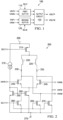
- FIG. 1 is an abstracted schematic diagram of a multiplexer 100 according to an embodiment of the disclosure.
- the multiplexer 100 comprises a first buffer 110, a second buffer 120, and an output circuit 130 coupled to the first buffer 110 and the second buffer 120.
- the first buffer 110 comprises logical inputs VINPO and VINMO
- the second buffer 120 comprises logical inputs VINP1 and VINM1.
- the multiplexer 100 and its components are described more fully below.
- FIG. 2 is a schematic diagram of a buffer 200 according to an embodiment of the disclosure.
- the buffer 200 may implement the first buffer 110.
- the buffer 200 comprises a source voltage 205; transistors 210, 240, 245, 250, 255, 260, 265, 270 (210-270); a current source 215; inductors 220, 225; resistors 230, 235; and a ground 275, all connected as shown in FIG. 2 .
- the buffer 200 comprises two selection inputs SELP; logical inputs VINPO, VINMO; and logical outputs VINP0', VINMO'.
- the source voltage 205 provides any suitable voltage. For instance, the source voltage 205 provides a voltage of about 5 volts (V) or less.
- the buffer 200 may not have its own power source on its chip. In that case, the source voltage 205 is a connection to an actual source voltage.
- the current source 215 provides any suitable constant current. For instance, the current source 215 provides a current of about 3 milliamps (mA) or less.
- the inductors 220, 225 compensate for or reduce parasitic capacitance in the buffer 200, thereby extending an operational bandwidth of the buffer 200.
- the inductors 220, 225 provide any suitable inductance values. For instance, the inductors 220, 225 provide inductance values between about 400 picohenries (pH) and about 600 pH.
- the resistors 230, 235 provide a load for the buffer 200.
- the resistors 230, 235 provide any suitable resistance values.
- the resistors 230, 235 provide resistive values between about 100 ohms ( ⁇ ) and about 200 ⁇ .
- the transistors 210, 240, 245, 250, 255, 260, 265, 270 comprise both a p-type enhancement mode transistor 210 and n-type enhancement mode transistors 240, 245, 250, 255, 260, 265, 270 (240-270).
- FIG. 3 is a schematic diagram of the p-type enhancement mode transistor 210 in FIG. 2 .
- the transistor 210 is a p-type metal-oxide-semiconductor field-effect transistor (MOSFET), or PMOS.
- the transistor 210 comprises a gate 310, a source 320, and a drain 330.
- the gate 310 receives a logical 0
- the transistor 210 is "turned on,” meaning that the source 320 and the drain 330 electrically couple to each other to allow a current to flow between them.
- the transistor 210 receives a logical 1
- the transistor 210 is "turned off,” meaning that the source 320 and the drain 330 do not electrically couple to each other to allow a current to flow between them.
- the transistor 210 acts as an open circuit between the source 320 and the drain 330.
- FIG. 4 is a schematic diagram of the n-type enhancement mode transistors 240-270 in FIG. 2 .
- the transistors 240-270 are n-type MOSFETs, or NMOSs.
- the transistors 240-270 comprise a gate 410, a drain 420, and a source 430.
- the gate 410 receives a logical 0, the transistors 240-270 are turned off, meaning that the drain 420 and the source 430 do not electrically couple to each other to allow a current to flow between them.
- the transistors 240-270 act as an open circuit between the drain 420 and the source 430.
- the transistors 240-270 When the gate 410 receives a logical 1, the transistors 240-270 are turned on, meaning that the drain 420 and the source 430 electrically couple to each other to allow a current to flow between them.
- the transistor 210 in operation when the selection inputs SELP receive a selection signal that is a logical 0, the transistor 210 is turned on and couples the source voltage 205 to the transistors 240, 245. In addition, the transistors 260, 265, 270 (260-270) are turned off and uncouple from the ground 275.
- the buffer 200 receives a differential logical input signal, specifically a logical high input signal at the logical input VINPO and a logical low input signal at the logical input VINMO.
- the transistor 240 is turned on, so the logical output VINMO', which is connected to the drain of the transistor 240, receives a voltage that is about equivalent to the voltage from the source voltage 205 minus a voltage drop across the resistor 230. The total voltage approximates a logical low signal.
- the logical output VINMO' provides a logical low output signal.
- the transistor 245 is turned off, so the logical output VINP0', which is connected to the drain of the transistor 245, receives a voltage of about the source voltage 205. That voltage approximates a logical high signal.
- the logical output VINP0' provides a logical high output signal.
- the logical low output signal at VINMO' and the logical high output signal at VINP0' form a differential logical output signal.
- the transistor 210 When the selection inputs SELP receive a selection signal that is a logical 1, the transistor 210 is turned off and uncouples the source voltage 205 from the transistors 240, 245, the drains of which are connected to the logical outputs VINMO', VINP0', respectively. At the same time, the transistors 260-270 are turned on and couple the logical outputs VINP0', VINMO' to the ground 275. Thus, the logical outputs VINP0', VINMO' provide logical low output signals. As can be seen, based on the selection inputs SELP, the buffer 200 either provides a differential logical output signal or provides no signal at all.
- Table 1 is a simplified logic table for the buffer 200. Table 1. Simplified logic table for the buffer 200 SELP VINP0' VINM0' 0 VINM0 VINP0 1 0 0 Table 1 is simplified in that logical values are not listed in every cell. For instance, when the selection signal at the selection inputs SELP is 0, the logical output VINP0' provides whatever logical input signal the logical input VINMO receives, and the logical output VINMO' provides whatever logical input signal the logical input VINPO receives. When the selection signal at the selection inputs SELP is 1, the logical outputs VINP0', VINMO' provide logical low output signals.
- the buffer 200 may implement the first buffer 110.
- a mirror image of the buffer 200 may implement the second buffer 120.
- the mirror image comprises two selection inputs SELM; logical inputs VINP1, VINM1; and logical outputs VINP1 ', VINM1'.
- the selection inputs SELP drive the first buffer 110
- the selection inputs SELM drive the second buffer 120.
- the selection inputs SELP drive the second buffer 120.
- FIG. 5 is a detailed schematic diagram of the output circuit 130 in FIG. 1 .
- the output circuit 130 comprises a source voltage 505 similar to the source voltage 205; inductors 510, 555 similar to the inductors 220, 225; resistors 515, 550 similar to the resistors 230, 235; transistors 520, 525, 540, 545 (520-545) similar to the transistors 210-270; a current source 530 similar to the current source 215; and a ground 535 similar to the ground 275.
- the output circuit 130 comprises logical inputs VINPO", VINMO", VINP1", VINM1” and multiplexer outputs VOUTP, VOUTM.
- the logical inputs VINPO", VINMO", VINP1", VINM1” correspond to the logical outputs VINP0', VINMO', VINP1', VINM1', respectively, from the first buffer 110 and the second buffer 120.
- the transistors 520-545 are directly coupled to the current source.
- the transistors 520, 525 are directly coupled to each other; the logical inputs VINPO", VINMO", respectively; and the multiplexer outputs VOUTM, VOUTP, respectively.
- the transistors 540, 545 are directly coupled to each other; the logical inputs VINP1", VINM1", respectively; and the multiplexer outputs VOUTM, VOUTP, respectively.
- the output circuit 130 receives no differential logical output signal from the second buffer 120, but does receive a differential logical output signal from the first buffer 110. Specifically, the output circuit 130 receives a logical low input signal at the logical input VINP0" and a logical high input signal at the logical input VINMO". In that case, the transistor 520 is turned off, so the multiplexer output VOUTM, which is connected to the drain of the transistor 520, receives a voltage of about the source voltage 505. That voltage approximates a logical high signal. Thus, the multiplexer output VOUTM provides a logical high output signal.
- the transistor 525 is turned on, so the multiplexer output VOUTP, which is connected to the drain of the transistor 525, receives a voltage that is equivalent to the voltage from the source voltage 505 minus a voltage drop across the resistor 550. The total voltage approximates a logical low signal. Thus, the multiplexer output VOUTP provides a logical low output signal.
- the output circuit 130 receives no differential logical output signal from the first buffer 110, but does receive a differential logical output signal from the second buffer 120. Specifically, the output circuit 130 receives a logical low input signal at the logical input VINM1" and a logical high input signal at the logical input VINP1". In that case, the transistor 545 is turned off, so the multiplexer output VOUTP, which is connected to the drain of the transistor 545, receives a voltage of about the source voltage 505. That voltage approximates a logical high signal. Thus, the multiplexer output VOUTP provides a logical high output signal.
- the transistor 540 is turned on, so the multiplexer output VOUTM, which is connected to the drain of the transistor 540, receives a voltage that is equivalent to the voltage from the source voltage 505 minus a voltage drop across the resistor 515. The total voltage approximates a logical low signal. Thus, the multiplexer output VOUTM provides a logical low output signal.
- Table 2 is a simplified logic table for the output circuit 130. Table 2. Simplified logic table for the output circuit 130 VINP0" VINM0" VINP1" VINM1" VOUTP VOUTM VINM0 VINP0 0 0 VINP0 VINM0 0 0 VINM1 VINP1 VINP1 VINM1 Table 2 is simplified in that logical values are not listed in every cell.
- the multiplexer output VOUTP provides whatever logical input signal the logical input VINPO receives and the multiplexer output VOUTM provides whatever logical input signal the logical input VINM0 receives.
- the multiplexer output VOUTP provides whatever logical input signal the logical input VINP1 receives and the multiplexer output VOUTM provides whatever logical input signal the logical input VINM1 receives.
- the output circuit 130 receives a differential logical output signal either from the first buffer 110 or the second buffer 120. However, the output circuit 130 does not receive a first differential logical output signal from the first buffer 110 and a second differential logical output signal from the second buffer 120 at the same time. As a result, the output circuit 130 is immunized from the first differential logical output signal interfering with the second differential logical output signal. In addition, such immunization enables the source voltages 205, 505 in the multiplexer 100 to operate at relatively lower voltages.
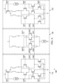
- FIG. 6 is a detailed schematic diagram of the multiplexer 100 in FIG. 1 .
- FIG. 6 shows the first buffer 110, the second buffer 120, and the output circuit 130.
- the buffers 110 and 120 are similar to or the same as the buffer 200 of FIG. 2
- the circuit 130 is the same as the output circuit 130 of FIG. 5 . Accordingly, the operation described therefore applies here in FIG. 6 .
- FIG. 6 also shows each component of the first buffer 110, the second buffer 120, and the output circuit 130. For instance, FIG.
- FIG. 6 shows that the logical output VINP0' of the first buffer 110 couples to the logical input VINP0" of the output circuit 130, the logical output VINM0' of the first buffer 110 couples to the logical input VINMO" of the output circuit 130, the logical output VINP1' of the second buffer 120 couples to the logical input VINP1" of the output circuit 130, and the logical output VINM1' of the second buffer 120 couples to the logical input VINM1 " of the output circuit 130.
- Table 3 is a simplified logic table for the multiplexer 100. Table 3 combines the logic of both Table 1 and Table 2. Table 3. Simplified logic table for the output multiplexer 100 SELP SELM VOUTP VOUTM 0 1 VINP0 VINM0 1 0 VINP1 VINM1 Table 3 is simplified in that logical values are not listed in every cell. For instance, when the selection signal at the selection inputs SELP is 0 and the selection signal at the selection inputs SELM is 1, the multiplexer output VOUTP provides whatever logical input signal the logical input VINP0 receives and the multiplexer output VOUTM provides whatever logical input signal the logical input VINM0 receives.
- the multiplexer output VOUTP provides whatever logical input signal the logical input VINP1 receives and the multiplexer output VOUTM provides whatever logical input signal the logical input VINM1 receives.
- the multiplexer 100 receives a logical high input signal from another component, then the multiplexer 100 uses inverter logic to provide a logical low input signal in order to form a differential input signal, meaning a signal having two voltage levels with respect to ground. The multiplexer 100 may do so for both logical input signals and selection signals. In a second embodiment, the multiplexer 100 receives differential logical input signals and differential selection signals form another component. In a third embodiment, the multiplexer 100 receives and provides single-ended signals, meaning signals having one voltage level with respect to ground.
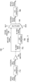
- FIG. 7 is a schematic diagram of an optical transceiver 700 according to an embodiment of the disclosure.
- the transceiver 700 comprises an optical-to-electrical (O-E) converter 710, an amplifier 720, a bypass mode path 730, a re-timer mode path 740, a clock and data recovery (CDR) component 750, the multiplexer 100, and an electrical-to-optical (E-O) converter 760.
- the components of the transceiver 700 may be arranged as shown or in any other suitable manner.
- the O-E converter 710 receives an optical input signal and converts the optical input signal to an electrical input signal.
- the amplifier 720 receives and amplifies the electrical input signal to produce an amplified signal.
- the amplified signal then follows both the bypass mode path 730 to the multiplexer 100 and the re-timer mode path 740 to the CDR component 750.
- the CDR component 750 receives the amplified signal and recovers data from the amplified signal. For instance, if the amplified signal comprises clock data, then the CDR component 750 recovers the clock data from the amplified signal with or without a local clock signal. The CDR component 750 then re-times the amplified signal with the recovered clock data to produce and re-timed signal to the multiplexer 100.
- the multiplexer 100 is referred to as a two-to-one (2:1) multiplexer because it receives two input signals, namely the amplified signal and the re-timed signal, and it provides one output signal, namely the electrical output signal.
- the multiplexer 100 functions as described above. Specifically, when the selection input SELP receives a selection signal that is a 0 and the selection input SELM receives a selection signal that is a 1, the multiplexer 100 provides the amplified signal to the E-O converter 760 and couples the re-timed signal to ground. In other words, only the bypass mode path 730 provides a signal to the E-O converter 760 through the multiplexer 100.
- the multiplexer 100 When the selection input SELP receives a selection signal that is a 1 and the selection input SELM receives a selection signal that is a 0, the multiplexer 100 provides the re-timed signal and couples the amplified signal to ground. In other words, only the re-timer mode path 740 provides a signal to the E-O converter 760 through the multiplexer 100. Finally, the E-O converter 760 converts, depending on what the multiplexer 100 provides, either the amplified signal or the re-timed signal to an optical output signal.
- the multiplexer 100 may switch back and forth between the bypass mode path 730 and the re-timer mode path 740 at a high data rate. Typically, this would introduce jitter. However, the multiplexer 100 either provides a signal from the bypass mode path 730 while coupling the re-timer mode path 740 to ground or provides a signal from the re-timer mode path 740 while coupling the bypass mode path 730 to ground. Thus, the multiplexer 100 eliminates or substantially eliminates such jitter.
- FIG. 7 shows the multiplexer 100 in the context of a function that selects either an amplified signal or a re-timed signal.
- the multiplexer 100 may perform a function that selects between more than two input signals. If there are more than two input signals, then the multiplexer may provide a corresponding number of buffers 200. For instance, to implement a 4:1 multiplexer, the multiplexer 100 may provide four of the buffers 200.
- FIG. 7 shows the multiplexer 100 in the context of optical signals. However, the multiplexer 100 may be a part of purely electrical components or systems.
- FIG. 8 is a flowchart illustrating a method 800 of signal selection according to an embodiment of the disclosure.
- the multiplexer 100 may implement the method 800.
- a selection signal and a logical input signal are received.
- the selection inputs SELP receive a selection signal and the logical inputs VINPO, VINMO receive a logical input signal.
- the logical inputs are coupled to multiplexer outputs when the selection signal is a first value.
- the logical inputs VINP0, VINM0 are coupled to the multiplexer outputs VOUTP, VOUTM when the selection signal is 0.
- the logical inputs are coupled to a ground when the selection signal is a second value.
- the logical inputs VINP0, VINM0 are coupled to the ground 275 when the selection signal is 1.
- the multiplexer 100 may implement the method 800 in the transceiver 700 as described above. In that case, the multiplexer 100 may switch back and forth between the bypass mode path 730 and the re-timer mode path 740 at a high data rate. Furthermore, the multiplexer 100 may eliminate or substantially eliminate jitter while doing so as also described above.
- FIG. 9 is a schematic diagram of a device 900 according to an embodiment of the disclosure.
- the device 900 is suitable for implementing the disclosed embodiments as described below.
- the device 900 comprises ingress ports 910 and receiver units (Rx) 920 for receiving data; a processor, logic unit, or central processing unit (CPU) 930 to process the data; transmitter units (Tx) 940 and egress ports 950 for transmitting the data; and a memory 960 for storing the data.
- the device 900 may also comprise O-E components and E-O components coupled to the ingress ports 910, the receiver units 920, the transmitter units 940, and the egress ports 950 for egress or ingress of optical or electrical signals.
- the processor 930 is implemented by hardware and software.
- the processor 930 may be implemented as one or more CPU chips, cores (e.g., as a multi-core processor), field-programmable gate arrays (FPGAs), application specific integrated circuits (ASICs), and digital signal processors (DSPs).
- the processor 930 is in communication with the ingress ports 910, receiver units 920, transmitter units 940, egress ports 950, and memory 960.
- the processor 930 is coupled to a multiplexer 970.
- the multiplexer 970 implements the disclosed embodiments described above. For instance, the multiplexer 970 implements the multiplexer 100 and receiving selection signals from the processor 930. The inclusion of the multiplexer 970 therefore provides a substantial improvement to the functionality of the device 900 and effects a transformation of the device 900 to a different state.
- the memory 960 comprises one or more disks, tape drives, and solid-state drives and may be used as an over-flow data storage device, to store programs when such programs are selected for execution, and to store instructions and data that are read during program execution.
- the memory 960 may be volatile and non-volatile and may be read-only memory (ROM), random-access memory (RAM), ternary content-addressable memory (TCAM), and static random-access memory (SRAM).
- One embodiment of the invention comprises an apparatus that includes bypass means to for creating a bypass mode path configured to provide a first signal.
- the apparatus further includes re-timer means for creating a a re-timer mode path comprising a clock and data recovery (CDR) component means configured to provide a re-timed signal based on the first signal.
- CDR clock and data recovery
- the apparatus includes a multiplexer means coupled to the bypass mode path and the re-timer mode path and configured to:
- a first component is directly coupled to a second component when there are no intervening components, except for a line, a trace, or other media, between the first component and the second component.
- the first component is indirectly coupled to the second component when there are intervening components between the first component and the second component.
- the termed "coupled” and its derivatives includes both directly coupled and indirectly coupled.
- the use of the term “about” means a range including ⁇ 10% of the subsequent number, unless otherwise stated.
Landscapes
- Engineering & Computer Science (AREA)
- Computer Networks & Wireless Communication (AREA)
- Signal Processing (AREA)
- Microelectronics & Electronic Packaging (AREA)
- Electronic Switches (AREA)
Description
- This application relates to switching systems and, more particularly, multiplexers.
- A multiplexer is a device that receives multiple input signals, selects one of the input signals, and provides that input signal as an output signal. The multiplexer selects the input signal based on a selection signal, which the multiplexer receives from a controller. For example, if the multiplexer receives a low voltage signal, or a logical 0, as a selection signal, then the multiplexer selects and provides a first input signal. If the multiplexer receives a high voltage signal, or a logical 1, as a selection signal, then the multiplexer selects and provides a second input signal.
US 5 334 881 A refers to a high isolation electronic switch for selectively switching an output line between first and second input lines.
US 6 720 818 B1 refers to a differential multiplexer for maximizing an amplitude of a differential output signal.
WO 2005 / 0 914 98 A1 refers to an analog signal switch circuit for selecting a first or second analog output state.
EP 1 278 320 A2 refers to a synchronous data serialization circuit.
US 2005 / 169 585 A1 refers to a XFP transceiver that includes CDR bypass functionality. - The invention is set out in the appended independent claims. Further embodiments are set out in the appended dependent claims.
- In a non-claimed example, the disclosure includes a multiplexer comprising: an output circuit comprising a multiplexer output; and a first buffer coupled to the output circuit and comprising: a first selection input configured to receive a first selection signal; a first logical input configured to receive a first logical input signal; and a first ground; wherein the multiplexer is configured to: couple the first logical input to the multiplexer output when the first selection signal is a first value; and couple the first logical input to the first ground when the first selection signal is a second value. In some embodiments, the first buffer further comprises a first logical output coupled to the output circuit; the first selection input comprises a second selection input and a third selection input, wherein the first logical input is a differential first logical input comprising a second logical input and a third logical input, and wherein the first logical output is a differential first logical output comprising a second logical output and a third logical output; the first buffer further comprises: a voltage source; a first transistor coupled to the voltage source and the second selection input; a second transistor coupled to the second selection input and the first ground; a third transistor coupled to the second selection input, the first ground, and the third logical output; and a fourth transistor coupled to the second selection input, the first ground, and the second logical output; the first transistor is a p-type metal-oxide-semiconductor (PMOS) transistor, and wherein the second transistor, the third transistor, and the fourth transistor are n-type metal-oxide-semiconductors (NMOSs); the multiplexer further comprises: a second buffer that is a mirror image of the first buffer and is coupled to the output circuit; the multiplexer further comprises: a second buffer coupled to the output circuit and comprising: a second selection input configured to receive a second selection signal; a second logical input configured to receive a second logical input signal; and a second ground; the multiplexer is further configured to: couple the second logical input to the multiplexer output when the second selection signal is the first value; couple the second logical input to the second ground when the second selection signal is the second value; the first ground and the second ground are the same; the multiplexer output is a differential multiplexer output comprising a first multiplexer output and a second multiplexer output; the output circuit further comprises: a first logical input coupled to the first buffer; a second logical input coupled to the first buffer; a third logical input; a fourth logical input; a current source; and a second ground coupled to the current source; the output circuit further comprises: a first transistor directly coupled to the first multiplexer output and the current source; a second transistor directly coupled to the second multiplexer output and the current source; a third transistor directly coupled to the first multiplexer output and the current source; and a fourth transistor directly coupled to the second multiplexer output and the current source; the first transistor, the second transistor, the third transistor, and the fourth transistor are n-type metal-oxide-semiconductor (NMOS) transistors.
- In another non-claimed example, the disclosure includes an apparatus comprising: a bypass mode path configured to provide a first signal; a re-timer mode path comprising a clock and data recovery (CDR) component configured to provide a re-timed signal based on the first signal; and a multiplexer coupled to the bypass mode path and the re-timer mode path and configured to: receive a selection signal; select the first signal and couple the re-timed signal to a ground when the selection signal is a first value; and select the re-timed signal and couple the first signal to the ground when the selection signal is a second value. In some embodiments, the multiplexer comprises a first buffer configured to: pass the first signal when the selection signal is the first value; and couple the first signal to a ground when the selection signal is the second value; the multiplexer further comprises a second buffer configured to: couple the re-timed signal to the ground when selection signal is the first value; and pass the re-timed signal when the selection signal is the second value.
- In yet another non-claimed example, the disclosure includes a method comprising: receiving a selection signal and a first logical input signal; coupling a first logical input to a multiplexer output when the selection signal is a first value; and coupling the first logical input to a ground when the selection signal is a second value. In some embodiments, the method further comprises: passing the first logical input signal through a first buffer and an output circuit when the selection signal is the first value; and coupling the first logical input signal to the ground through the first buffer when the selection signal is the second value; the method further comprises: receiving a second logical input signal; coupling a second logical input to the ground when the selection signal is the first value; and coupling the second logical input to the multiplexer output when the selection signal is the second value; the method further comprises: coupling the second logical input signal to the ground through a second buffer when the selection signal is the first value; and passing the second logical input signal through the second buffer and the output circuit when the selection signal is the second value.
- For a more complete understanding of this disclosure, reference is now made to the following brief description, taken in connection with the accompanying drawings and detailed description, wherein like reference numerals represent like parts.
-
FIG. 1 is an abstracted schematic diagram of a multiplexer according to an embodiment of the disclosure. -
FIG. 2 is a schematic diagram of a buffer according to an embodiment of the disclosure. -
FIG. 3 is a schematic diagram of the p-type enhancement mode transistor inFIG. 2 . -
FIG. 4 is a schematic diagram of the n-type enhancement mode transistors inFIG. 2 . -
FIG. 5 is a detailed schematic diagram of the output circuit inFIG. 1 . -
FIG. 6 is a detailed schematic diagram of the multiplexer inFIG. 1 . -
FIG. 7 is a schematic diagram of an optical transceiver according to an embodiment of the disclosure. -
FIG. 8 is a flowchart illustrating a method of signal selection according to an embodiment of the disclosure. -
FIG. 9 is a schematic diagram of a device according to an embodiment of the disclosure. - It should be understood at the outset that, although an illustrative implementation of one or more embodiments are provided below, the disclosed systems and/or methods may be implemented using any number of techniques, whether currently known or in existence. The disclosure should in no way be limited to the illustrative implementations, drawings, and techniques illustrated below, including the exemplary designs and implementations illustrated and described herein, but may be modified within the scope of the appended claims along with their full scope of equivalents.
- A multiplexer, for instance a multiplexer operating at a bit rate at or above 15 gigabits per second (Gb/s), may experience performance degradation. Specifically, even though the multiplexer has an unselected input signal and a selected input signal, the unselected input signal may interference with the selected input signal and cause the multiplexer to experience jitter at its output. Jitter is defined as a deviation from periodicity, typically in relation to a reference clock. It is therefore desirable to reduce or eliminate, and therefore immunize multiplexers from, such interference.
- Disclosed herein are embodiments for interference-immunized multiplexers. The disclosed multiplexers comprise a first buffer circuit, a second buffer circuit, and an output circuit coupled to the first buffer circuit and the second buffer circuit. The first buffer circuit and the second buffer circuit replace single transistors that exist in other multiplexers. Those single transistors receive selection signals and are coupled in series to corresponding differential inputs and a corresponding output. Instead, the first buffer circuit and the second buffer circuit either provide differential output signals when they are selected by a selection signal or do not provide the differential output signals when they are not selected by the selection signal. In the latter case, outputs of the first buffer circuit and the second buffer circuit are tied to ground. As a result, the disclosed multiplexers are substantially or completely immunized from unselected input signal interference. In addition, such immunization enables the disclosed multiplexers to operate at relatively lower supply voltages.
-
FIG. 1 is an abstracted schematic diagram of amultiplexer 100 according to an embodiment of the disclosure. Themultiplexer 100 comprises afirst buffer 110, asecond buffer 120, and anoutput circuit 130 coupled to thefirst buffer 110 and thesecond buffer 120. Thefirst buffer 110 comprises logical inputs VINPO and VINMO, and thesecond buffer 120 comprises logical inputs VINP1 and VINM1. Themultiplexer 100 and its components are described more fully below. -
FIG. 2 is a schematic diagram of abuffer 200 according to an embodiment of the disclosure. Thebuffer 200 may implement thefirst buffer 110. Thebuffer 200 comprises asource voltage 205;transistors current source 215;inductors resistors ground 275, all connected as shown inFIG. 2 . In addition, thebuffer 200 comprises two selection inputs SELP; logical inputs VINPO, VINMO; and logical outputs VINP0', VINMO'. - The
source voltage 205 provides any suitable voltage. For instance, thesource voltage 205 provides a voltage of about 5 volts (V) or less. Thebuffer 200 may not have its own power source on its chip. In that case, thesource voltage 205 is a connection to an actual source voltage. Thecurrent source 215 provides any suitable constant current. For instance, thecurrent source 215 provides a current of about 3 milliamps (mA) or less. - The
inductors buffer 200, thereby extending an operational bandwidth of thebuffer 200. Theinductors inductors - The
resistors buffer 200. Theresistors resistors transistors enhancement mode transistor 210 and n-typeenhancement mode transistors -
FIG. 3 is a schematic diagram of the p-typeenhancement mode transistor 210 inFIG. 2 . Thetransistor 210 is a p-type metal-oxide-semiconductor field-effect transistor (MOSFET), or PMOS. Thetransistor 210 comprises agate 310, asource 320, and adrain 330. When thegate 310 receives a logical 0, thetransistor 210 is "turned on," meaning that thesource 320 and thedrain 330 electrically couple to each other to allow a current to flow between them. When thegate 310 receives a logical 1, thetransistor 210 is "turned off," meaning that thesource 320 and thedrain 330 do not electrically couple to each other to allow a current to flow between them. Thus, thetransistor 210 acts as an open circuit between thesource 320 and thedrain 330. -
FIG. 4 is a schematic diagram of the n-type enhancement mode transistors 240-270 inFIG. 2 . The transistors 240-270 are n-type MOSFETs, or NMOSs. The transistors 240-270 comprise agate 410, adrain 420, and asource 430. When thegate 410 receives a logical 0, the transistors 240-270 are turned off, meaning that thedrain 420 and thesource 430 do not electrically couple to each other to allow a current to flow between them. Thus, the transistors 240-270 act as an open circuit between thedrain 420 and thesource 430. When thegate 410 receives a logical 1, the transistors 240-270 are turned on, meaning that thedrain 420 and thesource 430 electrically couple to each other to allow a current to flow between them. - Returning to
FIG. 2 , in operation when the selection inputs SELP receive a selection signal that is a logical 0, thetransistor 210 is turned on and couples thesource voltage 205 to thetransistors transistors ground 275. As an example, thebuffer 200 receives a differential logical input signal, specifically a logical high input signal at the logical input VINPO and a logical low input signal at the logical input VINMO. In that case, thetransistor 240 is turned on, so the logical output VINMO', which is connected to the drain of thetransistor 240, receives a voltage that is about equivalent to the voltage from thesource voltage 205 minus a voltage drop across theresistor 230. The total voltage approximates a logical low signal. Thus, the logical output VINMO' provides a logical low output signal. At the same time, thetransistor 245 is turned off, so the logical output VINP0', which is connected to the drain of thetransistor 245, receives a voltage of about thesource voltage 205. That voltage approximates a logical high signal. Thus, the logical output VINP0' provides a logical high output signal. Together, the logical low output signal at VINMO' and the logical high output signal at VINP0' form a differential logical output signal. - When the selection inputs SELP receive a selection signal that is a logical 1, the
transistor 210 is turned off and uncouples thesource voltage 205 from thetransistors ground 275. Thus, the logical outputs VINP0', VINMO' provide logical low output signals. As can be seen, based on the selection inputs SELP, thebuffer 200 either provides a differential logical output signal or provides no signal at all. - Table 1 is a simplified logic table for the
buffer 200.Table 1. Simplified logic table for the buffer 200SELP VINP0' VINM0' 0 VINM0 VINP0 1 0 0 - As mentioned above, the
buffer 200 may implement thefirst buffer 110. In addition, a mirror image of thebuffer 200 may implement thesecond buffer 120. However, the mirror image comprises two selection inputs SELM; logical inputs VINP1, VINM1; and logical outputs VINP1 ', VINM1'. Thus, if the selection inputs SELP drive thefirst buffer 110, then the selection inputs SELM drive thesecond buffer 120. Likewise, if the selection inputs SELM drive thefirst buffer 110, then the selection inputs SELP drive thesecond buffer 120. -
FIG. 5 is a detailed schematic diagram of theoutput circuit 130 inFIG. 1 . Theoutput circuit 130 comprises asource voltage 505 similar to thesource voltage 205;inductors inductors resistors resistors transistors current source 530 similar to thecurrent source 215; and aground 535 similar to theground 275. In addition, theoutput circuit 130 comprises logical inputs VINPO", VINMO", VINP1", VINM1" and multiplexer outputs VOUTP, VOUTM. The logical inputs VINPO", VINMO", VINP1", VINM1" correspond to the logical outputs VINP0', VINMO', VINP1', VINM1', respectively, from thefirst buffer 110 and thesecond buffer 120. - The transistors 520-545 are directly coupled to the current source. The
transistors transistors - In operation, in a first example, the
output circuit 130 receives no differential logical output signal from thesecond buffer 120, but does receive a differential logical output signal from thefirst buffer 110. Specifically, theoutput circuit 130 receives a logical low input signal at the logical input VINP0" and a logical high input signal at the logical input VINMO". In that case, thetransistor 520 is turned off, so the multiplexer output VOUTM, which is connected to the drain of thetransistor 520, receives a voltage of about thesource voltage 505. That voltage approximates a logical high signal. Thus, the multiplexer output VOUTM provides a logical high output signal. At the same time, thetransistor 525 is turned on, so the multiplexer output VOUTP, which is connected to the drain of thetransistor 525, receives a voltage that is equivalent to the voltage from thesource voltage 505 minus a voltage drop across theresistor 550. The total voltage approximates a logical low signal. Thus, the multiplexer output VOUTP provides a logical low output signal. - In a second example, the
output circuit 130 receives no differential logical output signal from thefirst buffer 110, but does receive a differential logical output signal from thesecond buffer 120. Specifically, theoutput circuit 130 receives a logical low input signal at the logical input VINM1" and a logical high input signal at the logical input VINP1". In that case, thetransistor 545 is turned off, so the multiplexer output VOUTP, which is connected to the drain of thetransistor 545, receives a voltage of about thesource voltage 505. That voltage approximates a logical high signal. Thus, the multiplexer output VOUTP provides a logical high output signal. At the same time, thetransistor 540 is turned on, so the multiplexer output VOUTM, which is connected to the drain of thetransistor 540, receives a voltage that is equivalent to the voltage from thesource voltage 505 minus a voltage drop across theresistor 515. The total voltage approximates a logical low signal. Thus, the multiplexer output VOUTM provides a logical low output signal. - Table 2 is a simplified logic table for the
output circuit 130.Table 2. Simplified logic table for the output circuit 130VINP0" VINM0" VINP1" VINM1" VOUTP VOUTM VINM0 VINP0 0 0 VINP0 VINM0 0 0 VINM1 VINP1 VINP1 VINM1 first buffer 110 and the logical inputs VINP 1", VINM1" do not receive a differential logical output signal from thesecond buffer 120, the multiplexer output VOUTP provides whatever logical input signal the logical input VINPO receives and the multiplexer output VOUTM provides whatever logical input signal the logical input VINM0 receives. When the logical inputs VINP1", VINM1" receive a differential logical output signal from thesecond buffer 120 and the logical inputs VINP0", VINM0" do not receive a differential logical output signal from thefirst buffer 110, the multiplexer output VOUTP provides whatever logical input signal the logical input VINP1 receives and the multiplexer output VOUTM provides whatever logical input signal the logical input VINM1 receives. - As can be seen, at any given time, the
output circuit 130 receives a differential logical output signal either from thefirst buffer 110 or thesecond buffer 120. However, theoutput circuit 130 does not receive a first differential logical output signal from thefirst buffer 110 and a second differential logical output signal from thesecond buffer 120 at the same time. As a result, theoutput circuit 130 is immunized from the first differential logical output signal interfering with the second differential logical output signal. In addition, such immunization enables the source voltages 205, 505 in themultiplexer 100 to operate at relatively lower voltages. -
FIG. 6 is a detailed schematic diagram of themultiplexer 100 inFIG. 1 . LikeFIG. 1 ,FIG. 6 shows thefirst buffer 110, thesecond buffer 120, and theoutput circuit 130. Thebuffers buffer 200 ofFIG. 2 , and thecircuit 130 is the same as theoutput circuit 130 ofFIG. 5 . Accordingly, the operation described therefore applies here inFIG. 6 . In addition, unlikeFIG. 1 ,FIG. 6 also shows each component of thefirst buffer 110, thesecond buffer 120, and theoutput circuit 130. For instance,FIG. 6 shows that the logical output VINP0' of thefirst buffer 110 couples to the logical input VINP0" of theoutput circuit 130, the logical output VINM0' of thefirst buffer 110 couples to the logical input VINMO" of theoutput circuit 130, the logical output VINP1' of thesecond buffer 120 couples to the logical input VINP1" of theoutput circuit 130, and the logical output VINM1' of thesecond buffer 120 couples to the logical input VINM1 " of theoutput circuit 130. - Table 3 is a simplified logic table for the
multiplexer 100. Table 3 combines the logic of both Table 1 and Table 2.Table 3. Simplified logic table for the output multiplexer 100SELP SELM VOUTP VOUTM 0 1 VINP0 VINM0 1 0 VINP1 VINM1 - In a first embodiment, the
multiplexer 100 receives a logical high input signal from another component, then themultiplexer 100 uses inverter logic to provide a logical low input signal in order to form a differential input signal, meaning a signal having two voltage levels with respect to ground. Themultiplexer 100 may do so for both logical input signals and selection signals. In a second embodiment, themultiplexer 100 receives differential logical input signals and differential selection signals form another component. In a third embodiment, themultiplexer 100 receives and provides single-ended signals, meaning signals having one voltage level with respect to ground. -
FIG. 7 is a schematic diagram of anoptical transceiver 700 according to an embodiment of the disclosure. Thetransceiver 700 comprises an optical-to-electrical (O-E)converter 710, anamplifier 720, abypass mode path 730, are-timer mode path 740, a clock and data recovery (CDR)component 750, themultiplexer 100, and an electrical-to-optical (E-O)converter 760. The components of thetransceiver 700 may be arranged as shown or in any other suitable manner. - The
O-E converter 710 receives an optical input signal and converts the optical input signal to an electrical input signal. Theamplifier 720 receives and amplifies the electrical input signal to produce an amplified signal. The amplified signal then follows both thebypass mode path 730 to themultiplexer 100 and there-timer mode path 740 to theCDR component 750. - The
CDR component 750 receives the amplified signal and recovers data from the amplified signal. For instance, if the amplified signal comprises clock data, then theCDR component 750 recovers the clock data from the amplified signal with or without a local clock signal. TheCDR component 750 then re-times the amplified signal with the recovered clock data to produce and re-timed signal to themultiplexer 100. - The
multiplexer 100 is referred to as a two-to-one (2:1) multiplexer because it receives two input signals, namely the amplified signal and the re-timed signal, and it provides one output signal, namely the electrical output signal. Themultiplexer 100 functions as described above. Specifically, when the selection input SELP receives a selection signal that is a 0 and the selection input SELM receives a selection signal that is a 1, themultiplexer 100 provides the amplified signal to theE-O converter 760 and couples the re-timed signal to ground. In other words, only thebypass mode path 730 provides a signal to theE-O converter 760 through themultiplexer 100. When the selection input SELP receives a selection signal that is a 1 and the selection input SELM receives a selection signal that is a 0, themultiplexer 100 provides the re-timed signal and couples the amplified signal to ground. In other words, only there-timer mode path 740 provides a signal to theE-O converter 760 through themultiplexer 100. Finally, theE-O converter 760 converts, depending on what themultiplexer 100 provides, either the amplified signal or the re-timed signal to an optical output signal. - The
multiplexer 100 may switch back and forth between thebypass mode path 730 and there-timer mode path 740 at a high data rate. Typically, this would introduce jitter. However, themultiplexer 100 either provides a signal from thebypass mode path 730 while coupling there-timer mode path 740 to ground or provides a signal from there-timer mode path 740 while coupling thebypass mode path 730 to ground. Thus, themultiplexer 100 eliminates or substantially eliminates such jitter. -
FIG. 7 shows themultiplexer 100 in the context of a function that selects either an amplified signal or a re-timed signal. However, themultiplexer 100 may perform a function that selects between more than two input signals. If there are more than two input signals, then the multiplexer may provide a corresponding number ofbuffers 200. For instance, to implement a 4:1 multiplexer, themultiplexer 100 may provide four of thebuffers 200. In addition,FIG. 7 shows themultiplexer 100 in the context of optical signals. However, themultiplexer 100 may be a part of purely electrical components or systems. -
FIG. 8 is a flowchart illustrating amethod 800 of signal selection according to an embodiment of the disclosure. Themultiplexer 100 may implement themethod 800. Atstep 810, a selection signal and a logical input signal are received. For instance, the selection inputs SELP receive a selection signal and the logical inputs VINPO, VINMO receive a logical input signal. Atstep 820, the logical inputs are coupled to multiplexer outputs when the selection signal is a first value. For instance, the logical inputs VINP0, VINM0 are coupled to the multiplexer outputs VOUTP, VOUTM when the selection signal is 0. Atstep 830, the logical inputs are coupled to a ground when the selection signal is a second value. For instance, the logical inputs VINP0, VINM0 are coupled to theground 275 when the selection signal is 1. - The
multiplexer 100 may implement themethod 800 in thetransceiver 700 as described above. In that case, themultiplexer 100 may switch back and forth between thebypass mode path 730 and there-timer mode path 740 at a high data rate. Furthermore, themultiplexer 100 may eliminate or substantially eliminate jitter while doing so as also described above. -
FIG. 9 is a schematic diagram of adevice 900 according to an embodiment of the disclosure. Thedevice 900 is suitable for implementing the disclosed embodiments as described below. Thedevice 900 comprisesingress ports 910 and receiver units (Rx) 920 for receiving data; a processor, logic unit, or central processing unit (CPU) 930 to process the data; transmitter units (Tx) 940 andegress ports 950 for transmitting the data; and amemory 960 for storing the data. Thedevice 900 may also comprise O-E components and E-O components coupled to theingress ports 910, thereceiver units 920, thetransmitter units 940, and theegress ports 950 for egress or ingress of optical or electrical signals. - The
processor 930 is implemented by hardware and software. Theprocessor 930 may be implemented as one or more CPU chips, cores (e.g., as a multi-core processor), field-programmable gate arrays (FPGAs), application specific integrated circuits (ASICs), and digital signal processors (DSPs). Theprocessor 930 is in communication with theingress ports 910,receiver units 920,transmitter units 940,egress ports 950, andmemory 960. Theprocessor 930 is coupled to amultiplexer 970. Themultiplexer 970 implements the disclosed embodiments described above. For instance, themultiplexer 970 implements themultiplexer 100 and receiving selection signals from theprocessor 930. The inclusion of themultiplexer 970 therefore provides a substantial improvement to the functionality of thedevice 900 and effects a transformation of thedevice 900 to a different state. - The
memory 960 comprises one or more disks, tape drives, and solid-state drives and may be used as an over-flow data storage device, to store programs when such programs are selected for execution, and to store instructions and data that are read during program execution. Thememory 960 may be volatile and non-volatile and may be read-only memory (ROM), random-access memory (RAM), ternary content-addressable memory (TCAM), and static random-access memory (SRAM). - One embodiment of the invention comprises an apparatus that includes bypass means to for creating a bypass mode path configured to provide a first signal. The apparatus further includes re-timer means for creating a a re-timer mode path comprising a clock and data recovery (CDR) component means configured to provide a re-timed signal based on the first signal. Finally the apparatus includes a multiplexer means coupled to the bypass mode path and the re-timer mode path and configured to:
- receive a selection signal;
- select the first signal and couple the re-timed signal to a ground when the selection signal is a first value; and
- select the re-timed signal and couple the first signal to the ground when the selection signal is a second value.
- A first component is directly coupled to a second component when there are no intervening components, except for a line, a trace, or other media, between the first component and the second component. The first component is indirectly coupled to the second component when there are intervening components between the first component and the second component. The termed "coupled" and its derivatives includes both directly coupled and indirectly coupled. The use of the term "about" means a range including ±10% of the subsequent number, unless otherwise stated. While several embodiments have been provided in the present disclosure, it may be understood that the disclosed systems and methods might be embodied in many other specific forms without departing from the scope of the present disclosure. The present examples are to be considered as illustrative and not restrictive, and the intention is not to be limited to the details given herein. For example, the various elements or components may be combined or integrated in another system or certain features may be omitted, or not implemented.
- In addition, techniques, systems, subsystems, and methods described and illustrated in the various embodiments as discrete or separate may be combined or integrated with other systems, components, techniques, or methods without departing from the scope of the present disclosure. Other items shown or discussed as coupled or directly coupled or communicating with each other may be indirectly coupled or communicating through some interface, device, or intermediate component whether electrically, mechanically, or otherwise.
Claims (12)
- A multiplexer (100) comprising:an output circuit (130) comprising multiplexer outputs (VOUTM, VOUTP) configured as a differential output;a first buffer (110, 200) coupled to the output circuit (130) and comprising:a first selection input (SELP) configured to receive a first logical selection signal; two first logical inputs (VINP0, VINM0) configured as a differential input and to receive a first logical input signal; anda first ground,wherein the first buffer (110) comprises two first logical outputs (VINP0', VINMO') configured as a differential output and coupled to the output circuit (130),a second buffer (120) that is a mirror image of the first buffer and is coupled to the output circuit (130), and comprises:a second selection input (SELM) configured to receive a second logical selection signal;two second logical inputs (VINP1, VINM1) configured as a differential input and to receive a second logical input signal;two second logical outputs (VINP1', VINM1') configured as a differential output and coupled to the output circuit (130); anda second ground,wherein the multiplexer (100) is configured to:couple the first logical inputs (VINP0, VINM0) to the multiplexer outputs (VOUTM, VOUTP) when the first logical selection signal is a first value,couple the first logical inputs (VINP0, VINM0) to the first ground when the first logical selection signal is a second value,couple the second logical inputs (VINP1, VINM1) to the multiplexer outputs (VOUTM, VOUTP) when the second logical selection signal is a first value; andcouple the second logical inputs (VINP1, VINM1) to the second ground when the second logical selection signal is a second value.
- The multiplexer (100) of claim 1, wherein the first buffer (110, 200) further comprises:a voltage source (205);a first transistor coupled to the voltage source (205) and the first selection input;a second transistor coupled to the first selection input and the first ground;a third transistor coupled to the first selection input, the first ground, and the one of the first logical outputs; anda fourth transistor coupled to the first selection input, the first ground, and the other one of the first logical outputs.
- The multiplexer (100) of claim 2, wherein the first transistor is a p-type metal-oxide-semiconductor (PMOS) transistor, and wherein the second transistor, the third transistor, and the fourth transistor are n-type metal-oxide-semiconductors (NMOSs).
- The multiplexer (100) of any one of claims 1-3, wherein the first ground and the second ground are the same.
- The multiplexer (100) of any one of claims 1-4, wherein the multiplexer output is a differential multiplexer output comprising a first multiplexer output and a second multiplexer output.
- The multiplexer (100) of any one of claims 1-5, wherein the output circuit (130) further comprises:a first logical input coupled to the first buffer (110);a second logical input coupled to the first buffer (110);a third logical input;a fourth logical input;a current source (215); anda second ground coupled to the current source. (215)
- The multiplexer (100) of any one of claims 1-6, wherein the output circuit (130) further comprises:a first transistor directly coupled to the first multiplexer output and the current source (215);a second transistor directly coupled to the second multiplexer output and the current source (215);a third transistor directly coupled to the first multiplexer output and the current source (215); anda fourth transistor directly coupled to the second multiplexer output and the current source (215).
- The multiplexer (100) of claim 7, wherein the first transistor, the second transistor, the third transistor, and the fourth transistor are n-type metal-oxide-semiconductor (NMOS) transistors.
- An apparatus (700) comprising:a bypass mode path (730) configured to provide a first signal;a re-timer mode path (740) comprising a clock and data recovery (CDR) component (750) configured to provide a re-timed signal based on the first signal; anda multiplexer (100) according to claims 1 to 8 coupled to the bypass mode path (730) and the re-timer mode path (740) and configured to:receive a selection signal;select the first signal and couple the re-timed signal to a ground when the selection signal is a first value; andselect the re-timed signal and couple the first signal to the ground when the selection signal is a second value.
- The apparatus (700) of claim 9, wherein the first buffer (110) of the multiplexer (100) is configured to:pass the first signal when the selection signal is the first value; andcouple the first signal to a ground when the selection signal is the second value.
- The apparatus (700) of any one of claims 9-10, wherein the second buffer (120) of the multiplexer (100) is configured to:couple the re-timed signal to the ground when selection signal is the first value; andpass the re-timed signal when the selection signal is the second value.
- A method (800) comprising:receiving (810) a first logical selection signal, and differentially receiving a first logical input signal via first logical inputs;differentially coupling (820) the first logical inputs to multiplexer outputs when the first logical selection signal is a first value,differentially coupling (830) the first logical inputs to a ground (275) when the first logical selection signal is a second value,differentially passing the first logical input signal through a first buffer (110) and an output circuit (130) when the first logical selection signal is the first value, wherein the first buffer (110) comprises first logical outputs differentially coupled to the output circuit (130),differentially coupling the first logical input signal to the ground through the first buffer (110) when the first logical selection signal is the second value,receiving a second logical selection signal, and differentially receiving a second logical input signal via second logical inputs;differentially coupling the second logical inputs to the ground (275) when the second logical selection signal is the first value,differentially coupling the second logical inputs to the multiplexer outputs when the second logical selection signal is the second value,differentially coupling the second logical input signal to the ground (275) through a second buffer (120), the second buffer (120) being a mirror image of the first buffer (110) and coupled to the output circuit (130), when the second logical selection signal is the first value,differentially passing the second logical input signal through the second buffer (120) and the output circuit (130) when the second logical selection signal is the second value.
Applications Claiming Priority (2)
| Application Number | Priority Date | Filing Date | Title |
|---|---|---|---|
| US15/084,918 US10122348B2 (en) | 2016-03-30 | 2016-03-30 | Interference-immunized multiplexer |
| PCT/CN2017/078590 WO2017167199A1 (en) | 2016-03-30 | 2017-03-29 | Interference-immunized multiplexer |
Publications (3)
| Publication Number | Publication Date |
|---|---|
| EP3430746A1 EP3430746A1 (en) | 2019-01-23 |
| EP3430746A4 EP3430746A4 (en) | 2019-07-31 |
| EP3430746B1 true EP3430746B1 (en) | 2024-11-27 |
Family
ID=59959837
Family Applications (1)
| Application Number | Title | Priority Date | Filing Date |
|---|---|---|---|
| EP17773229.4A Active EP3430746B1 (en) | 2016-03-30 | 2017-03-29 | Interference-immunized multiplexer |
Country Status (4)
| Country | Link |
|---|---|
| US (1) | US10122348B2 (en) |
| EP (1) | EP3430746B1 (en) |
| CN (1) | CN109075886B (en) |
| WO (1) | WO2017167199A1 (en) |
Families Citing this family (1)
| Publication number | Priority date | Publication date | Assignee | Title |
|---|---|---|---|---|
| US10951391B2 (en) * | 2015-09-06 | 2021-03-16 | Bar-Ilan University | Randomized logic against side channel attacks |
Family Cites Families (13)
| Publication number | Priority date | Publication date | Assignee | Title |
|---|---|---|---|---|
| US5334881A (en) * | 1992-03-19 | 1994-08-02 | The United States Of America As Represented By The Secretary Of The Navy | High isolation electronic switch |
| US6340899B1 (en) * | 2000-02-24 | 2002-01-22 | Broadcom Corporation | Current-controlled CMOS circuits with inductive broadbanding |
| US6614371B2 (en) * | 2001-07-19 | 2003-09-02 | Broadcom Corporation | Synchronous data serialization circuit |
| US7809275B2 (en) | 2002-06-25 | 2010-10-05 | Finisar Corporation | XFP transceiver with 8.5G CDR bypass |
| US6720818B1 (en) * | 2002-11-08 | 2004-04-13 | Applied Micro Circuits Corporation | Method and apparatus for maximizing an amplitude of an output signal of a differential multiplexer |
| US7233176B2 (en) | 2003-12-26 | 2007-06-19 | Stmicroelectronics Pvt. Ltd. | CMOS input buffer and a method for supporting multiple I/O standards |
| WO2005091498A1 (en) * | 2004-03-17 | 2005-09-29 | Asahi Kasei Microsystems Co., Ltd. | Signal switch circuit |
| US7463061B1 (en) * | 2005-07-19 | 2008-12-09 | Actel Corporation | Apparatus and method for reducing leakage of unused buffers in an integrated circuit |
| CN102300120B (en) | 2010-06-23 | 2015-06-10 | 中兴通讯股份有限公司 | Switch and method for selectively outputting multiple signals |
| US20120057606A1 (en) * | 2010-09-07 | 2012-03-08 | Broadcom Corporation | Multiplexer circuit |
| US8804437B2 (en) * | 2012-09-25 | 2014-08-12 | Nvidia Corporation | Column select multiplexer and method for static random-access memory and computer memory subsystem employing the same |
| US9658971B2 (en) * | 2013-09-11 | 2017-05-23 | Nxp Usa, Inc. | Universal SPI (serial peripheral interface) |
| US9832048B2 (en) * | 2015-08-24 | 2017-11-28 | Xilinx, Inc. | Transmitter circuit for and methods of generating a modulated signal in a transmitter |
-
2016
- 2016-03-30 US US15/084,918 patent/US10122348B2/en active Active
-
2017
- 2017-03-29 EP EP17773229.4A patent/EP3430746B1/en active Active
- 2017-03-29 WO PCT/CN2017/078590 patent/WO2017167199A1/en not_active Ceased
- 2017-03-29 CN CN201780019998.1A patent/CN109075886B/en active Active
Also Published As
| Publication number | Publication date |
|---|---|
| CN109075886A (en) | 2018-12-21 |
| EP3430746A1 (en) | 2019-01-23 |
| US10122348B2 (en) | 2018-11-06 |
| EP3430746A4 (en) | 2019-07-31 |
| US20170288652A1 (en) | 2017-10-05 |
| CN109075886B (en) | 2020-02-14 |
| WO2017167199A1 (en) | 2017-10-05 |
Similar Documents
| Publication | Publication Date | Title |
|---|---|---|
| US8520348B2 (en) | High-swing differential driver using low-voltage transistors | |
| US7495477B2 (en) | Apparatus and methods for self-biasing differential signaling circuitry having multimode output configurations for low voltage applications | |
| EP2798802B1 (en) | Tri-state control for a line driver | |
| US9484891B2 (en) | Multi-modal communication interface | |
| US9035677B2 (en) | High-speed low power stacked transceiver | |
| US7924055B2 (en) | Data transmitting system | |
| US8519771B1 (en) | Methods and apparatus for receiving high and low voltage signals using a low supply voltage technology | |
| US7629817B2 (en) | System and apparatus for aperture time improvement | |
| EP2111709A2 (en) | Differential receiver with common-gate input stage | |
| EP1269630A2 (en) | Current-controlled cmos circuits with inductive broadbanding | |
| US20120049897A1 (en) | Output buffer circuit and semiconductor device | |
| US11139843B1 (en) | SerDes driver with common-gate-based buffer to use core devices in relatively high power supply domain | |
| US10447269B1 (en) | Level shifter | |
| US10122348B2 (en) | Interference-immunized multiplexer | |
| US8253442B2 (en) | Apparatus and method for signal transmission over a channel | |
| EP2156559B1 (en) | Adjustable input receiver for low power high speed interface | |
| US7755684B2 (en) | Row driver circuitry for imaging devices and related method of operation | |
| KR102252820B1 (en) | Transmitter performing equalizing operation | |
| US10171711B1 (en) | De-emphasized image signal transmission | |
| US9515643B2 (en) | Hot-socket circuitry | |
| JP2008147940A (en) | Semiconductor integrated circuit | |
| US20040113659A1 (en) | High-resolution single-ended source-synchronous receiver | |
| HK1138951B (en) | Adjustable input receiver for low power high speed interface |
Legal Events
| Date | Code | Title | Description |
|---|---|---|---|
| STAA | Information on the status of an ep patent application or granted ep patent |
Free format text: STATUS: THE INTERNATIONAL PUBLICATION HAS BEEN MADE |
|
| PUAI | Public reference made under article 153(3) epc to a published international application that has entered the european phase |
Free format text: ORIGINAL CODE: 0009012 |
|
| STAA | Information on the status of an ep patent application or granted ep patent |
Free format text: STATUS: REQUEST FOR EXAMINATION WAS MADE |
|
| 17P | Request for examination filed |
Effective date: 20181017 |
|
| AK | Designated contracting states |
Kind code of ref document: A1 Designated state(s): AL AT BE BG CH CY CZ DE DK EE ES FI FR GB GR HR HU IE IS IT LI LT LU LV MC MK MT NL NO PL PT RO RS SE SI SK SM TR |
|
| AX | Request for extension of the european patent |
Extension state: BA ME |
|
| RIN1 | Information on inventor provided before grant (corrected) |
Inventor name: DESHPANDE, MAMATHA Inventor name: GU, LIANG Inventor name: SHIH, SHOU-PO Inventor name: LEI, GONG Inventor name: CAO, YUMING Inventor name: GU, YIFAN Inventor name: DANG, YEN Inventor name: DUAN, YAN Inventor name: LEE, HUNGYI |
|
| RIC1 | Information provided on ipc code assigned before grant |
Ipc: H03K 17/16 20060101ALI20190219BHEP Ipc: H04J 14/02 20060101AFI20190219BHEP |
|
| DAV | Request for validation of the european patent (deleted) | ||
| DAX | Request for extension of the european patent (deleted) | ||
| A4 | Supplementary search report drawn up and despatched |
Effective date: 20190702 |
|
| RIC1 | Information provided on ipc code assigned before grant |
Ipc: H03K 17/16 20060101ALI20190626BHEP Ipc: H04J 14/02 20060101AFI20190626BHEP |
|
| STAA | Information on the status of an ep patent application or granted ep patent |
Free format text: STATUS: EXAMINATION IS IN PROGRESS |
|
| 17Q | First examination report despatched |
Effective date: 20201214 |
|
| GRAP | Despatch of communication of intention to grant a patent |
Free format text: ORIGINAL CODE: EPIDOSNIGR1 |
|
| STAA | Information on the status of an ep patent application or granted ep patent |
Free format text: STATUS: GRANT OF PATENT IS INTENDED |
|
| INTG | Intention to grant announced |
Effective date: 20240719 |
|
| P01 | Opt-out of the competence of the unified patent court (upc) registered |
Free format text: CASE NUMBER: APP_48756/2024 Effective date: 20240827 |
|
| GRAS | Grant fee paid |
Free format text: ORIGINAL CODE: EPIDOSNIGR3 |
|
| GRAA | (expected) grant |
Free format text: ORIGINAL CODE: 0009210 |
|
| STAA | Information on the status of an ep patent application or granted ep patent |
Free format text: STATUS: THE PATENT HAS BEEN GRANTED |
|
| AK | Designated contracting states |
Kind code of ref document: B1 Designated state(s): AL AT BE BG CH CY CZ DE DK EE ES FI FR GB GR HR HU IE IS IT LI LT LU LV MC MK MT NL NO PL PT RO RS SE SI SK SM TR |
|
| REG | Reference to a national code |
Ref country code: GB Ref legal event code: FG4D |
|
| REG | Reference to a national code |
Ref country code: CH Ref legal event code: EP |
|
| REG | Reference to a national code |
Ref country code: IE Ref legal event code: FG4D |
|
| REG | Reference to a national code |
Ref country code: DE Ref legal event code: R096 Ref document number: 602017086389 Country of ref document: DE |
|
| REG | Reference to a national code |
Ref country code: LT Ref legal event code: MG9D |
|
| REG | Reference to a national code |
Ref country code: NL Ref legal event code: MP Effective date: 20241127 |
|
| PG25 | Lapsed in a contracting state [announced via postgrant information from national office to epo] |
Ref country code: PT Free format text: LAPSE BECAUSE OF FAILURE TO SUBMIT A TRANSLATION OF THE DESCRIPTION OR TO PAY THE FEE WITHIN THE PRESCRIBED TIME-LIMIT Effective date: 20250327 Ref country code: HR Free format text: LAPSE BECAUSE OF FAILURE TO SUBMIT A TRANSLATION OF THE DESCRIPTION OR TO PAY THE FEE WITHIN THE PRESCRIBED TIME-LIMIT Effective date: 20241127 Ref country code: IS Free format text: LAPSE BECAUSE OF FAILURE TO SUBMIT A TRANSLATION OF THE DESCRIPTION OR TO PAY THE FEE WITHIN THE PRESCRIBED TIME-LIMIT Effective date: 20250327 |
|
| PG25 | Lapsed in a contracting state [announced via postgrant information from national office to epo] |
Ref country code: NL Free format text: LAPSE BECAUSE OF FAILURE TO SUBMIT A TRANSLATION OF THE DESCRIPTION OR TO PAY THE FEE WITHIN THE PRESCRIBED TIME-LIMIT Effective date: 20241127 Ref country code: FI Free format text: LAPSE BECAUSE OF FAILURE TO SUBMIT A TRANSLATION OF THE DESCRIPTION OR TO PAY THE FEE WITHIN THE PRESCRIBED TIME-LIMIT Effective date: 20241127 |
|
| REG | Reference to a national code |
Ref country code: AT Ref legal event code: MK05 Ref document number: 1746740 Country of ref document: AT Kind code of ref document: T Effective date: 20241127 |
|
| PG25 | Lapsed in a contracting state [announced via postgrant information from national office to epo] |
Ref country code: BG Free format text: LAPSE BECAUSE OF FAILURE TO SUBMIT A TRANSLATION OF THE DESCRIPTION OR TO PAY THE FEE WITHIN THE PRESCRIBED TIME-LIMIT Effective date: 20241127 |
|
| PG25 | Lapsed in a contracting state [announced via postgrant information from national office to epo] |
Ref country code: ES Free format text: LAPSE BECAUSE OF FAILURE TO SUBMIT A TRANSLATION OF THE DESCRIPTION OR TO PAY THE FEE WITHIN THE PRESCRIBED TIME-LIMIT Effective date: 20241127 |
|
| PG25 | Lapsed in a contracting state [announced via postgrant information from national office to epo] |
Ref country code: NO Free format text: LAPSE BECAUSE OF FAILURE TO SUBMIT A TRANSLATION OF THE DESCRIPTION OR TO PAY THE FEE WITHIN THE PRESCRIBED TIME-LIMIT Effective date: 20250227 |
|
| PG25 | Lapsed in a contracting state [announced via postgrant information from national office to epo] |
Ref country code: LV Free format text: LAPSE BECAUSE OF FAILURE TO SUBMIT A TRANSLATION OF THE DESCRIPTION OR TO PAY THE FEE WITHIN THE PRESCRIBED TIME-LIMIT Effective date: 20241127 Ref country code: AT Free format text: LAPSE BECAUSE OF FAILURE TO SUBMIT A TRANSLATION OF THE DESCRIPTION OR TO PAY THE FEE WITHIN THE PRESCRIBED TIME-LIMIT Effective date: 20241127 Ref country code: GR Free format text: LAPSE BECAUSE OF FAILURE TO SUBMIT A TRANSLATION OF THE DESCRIPTION OR TO PAY THE FEE WITHIN THE PRESCRIBED TIME-LIMIT Effective date: 20250228 |
|
| PG25 | Lapsed in a contracting state [announced via postgrant information from national office to epo] |
Ref country code: PL Free format text: LAPSE BECAUSE OF FAILURE TO SUBMIT A TRANSLATION OF THE DESCRIPTION OR TO PAY THE FEE WITHIN THE PRESCRIBED TIME-LIMIT Effective date: 20241127 |
|
| PG25 | Lapsed in a contracting state [announced via postgrant information from national office to epo] |
Ref country code: RS Free format text: LAPSE BECAUSE OF FAILURE TO SUBMIT A TRANSLATION OF THE DESCRIPTION OR TO PAY THE FEE WITHIN THE PRESCRIBED TIME-LIMIT Effective date: 20250227 |
|
| PG25 | Lapsed in a contracting state [announced via postgrant information from national office to epo] |
Ref country code: SM Free format text: LAPSE BECAUSE OF FAILURE TO SUBMIT A TRANSLATION OF THE DESCRIPTION OR TO PAY THE FEE WITHIN THE PRESCRIBED TIME-LIMIT Effective date: 20241127 |
|
| PG25 | Lapsed in a contracting state [announced via postgrant information from national office to epo] |
Ref country code: DK Free format text: LAPSE BECAUSE OF FAILURE TO SUBMIT A TRANSLATION OF THE DESCRIPTION OR TO PAY THE FEE WITHIN THE PRESCRIBED TIME-LIMIT Effective date: 20241127 |
|
| PG25 | Lapsed in a contracting state [announced via postgrant information from national office to epo] |
Ref country code: EE Free format text: LAPSE BECAUSE OF FAILURE TO SUBMIT A TRANSLATION OF THE DESCRIPTION OR TO PAY THE FEE WITHIN THE PRESCRIBED TIME-LIMIT Effective date: 20241127 |
|
| PG25 | Lapsed in a contracting state [announced via postgrant information from national office to epo] |
Ref country code: RO Free format text: LAPSE BECAUSE OF FAILURE TO SUBMIT A TRANSLATION OF THE DESCRIPTION OR TO PAY THE FEE WITHIN THE PRESCRIBED TIME-LIMIT Effective date: 20241127 |
|
| PG25 | Lapsed in a contracting state [announced via postgrant information from national office to epo] |
Ref country code: SK Free format text: LAPSE BECAUSE OF FAILURE TO SUBMIT A TRANSLATION OF THE DESCRIPTION OR TO PAY THE FEE WITHIN THE PRESCRIBED TIME-LIMIT Effective date: 20241127 |
|
| PG25 | Lapsed in a contracting state [announced via postgrant information from national office to epo] |
Ref country code: CZ Free format text: LAPSE BECAUSE OF FAILURE TO SUBMIT A TRANSLATION OF THE DESCRIPTION OR TO PAY THE FEE WITHIN THE PRESCRIBED TIME-LIMIT Effective date: 20241127 |
|
| PG25 | Lapsed in a contracting state [announced via postgrant information from national office to epo] |
Ref country code: IT Free format text: LAPSE BECAUSE OF FAILURE TO SUBMIT A TRANSLATION OF THE DESCRIPTION OR TO PAY THE FEE WITHIN THE PRESCRIBED TIME-LIMIT Effective date: 20241127 |
|
| REG | Reference to a national code |
Ref country code: DE Ref legal event code: R097 Ref document number: 602017086389 Country of ref document: DE |
|
| PG25 | Lapsed in a contracting state [announced via postgrant information from national office to epo] |
Ref country code: SE Free format text: LAPSE BECAUSE OF FAILURE TO SUBMIT A TRANSLATION OF THE DESCRIPTION OR TO PAY THE FEE WITHIN THE PRESCRIBED TIME-LIMIT Effective date: 20241127 |
|
| PLBE | No opposition filed within time limit |
Free format text: ORIGINAL CODE: 0009261 |
|
| STAA | Information on the status of an ep patent application or granted ep patent |
Free format text: STATUS: NO OPPOSITION FILED WITHIN TIME LIMIT |
|
| REG | Reference to a national code |
Ref country code: CH Ref legal event code: L10 Free format text: ST27 STATUS EVENT CODE: U-0-0-L10-L00 (AS PROVIDED BY THE NATIONAL OFFICE) Effective date: 20251008 |
|
| PG25 | Lapsed in a contracting state [announced via postgrant information from national office to epo] |
Ref country code: MC Free format text: LAPSE BECAUSE OF FAILURE TO SUBMIT A TRANSLATION OF THE DESCRIPTION OR TO PAY THE FEE WITHIN THE PRESCRIBED TIME-LIMIT Effective date: 20241127 |
|
| REG | Reference to a national code |
Ref country code: CH Ref legal event code: H13 Free format text: ST27 STATUS EVENT CODE: U-0-0-H10-H13 (AS PROVIDED BY THE NATIONAL OFFICE) Effective date: 20251023 |
|
| 26N | No opposition filed |
Effective date: 20250828 |
|
| PG25 | Lapsed in a contracting state [announced via postgrant information from national office to epo] |
Ref country code: LU Free format text: LAPSE BECAUSE OF NON-PAYMENT OF DUE FEES Effective date: 20250329 |
|
| GBPC | Gb: european patent ceased through non-payment of renewal fee |
Effective date: 20250329 |
|
| REG | Reference to a national code |
Ref country code: BE Ref legal event code: MM Effective date: 20250331 |
|
| PG25 | Lapsed in a contracting state [announced via postgrant information from national office to epo] |
Ref country code: GB Free format text: LAPSE BECAUSE OF NON-PAYMENT OF DUE FEES Effective date: 20250329 |
|
| PG25 | Lapsed in a contracting state [announced via postgrant information from national office to epo] |
Ref country code: BE Free format text: LAPSE BECAUSE OF NON-PAYMENT OF DUE FEES Effective date: 20250331 |
|
| PG25 | Lapsed in a contracting state [announced via postgrant information from national office to epo] |
Ref country code: CH Free format text: LAPSE BECAUSE OF NON-PAYMENT OF DUE FEES Effective date: 20250331 |
|
| PG25 | Lapsed in a contracting state [announced via postgrant information from national office to epo] |
Ref country code: IE Free format text: LAPSE BECAUSE OF NON-PAYMENT OF DUE FEES Effective date: 20250329 |
|
| PGFP | Annual fee paid to national office [announced via postgrant information from national office to epo] |
Ref country code: DE Payment date: 20260204 Year of fee payment: 10 |
|
| PGFP | Annual fee paid to national office [announced via postgrant information from national office to epo] |
Ref country code: FR Payment date: 20260209 Year of fee payment: 10 |