EP3430728B1 - Communication circuit for multi-antenna apparatus - Google Patents
Communication circuit for multi-antenna apparatus Download PDFInfo
- Publication number
- EP3430728B1 EP3430728B1 EP16711591.4A EP16711591A EP3430728B1 EP 3430728 B1 EP3430728 B1 EP 3430728B1 EP 16711591 A EP16711591 A EP 16711591A EP 3430728 B1 EP3430728 B1 EP 3430728B1
- Authority
- EP
- European Patent Office
- Prior art keywords
- radio
- loa
- units
- frequency
- signals
- Prior art date
- Legal status (The legal status is an assumption and is not a legal conclusion. Google has not performed a legal analysis and makes no representation as to the accuracy of the status listed.)
- Active
Links
Images


Classifications
-
- H—ELECTRICITY
- H04—ELECTRIC COMMUNICATION TECHNIQUE
- H04B—TRANSMISSION
- H04B7/00—Radio transmission systems, i.e. using radiation field
- H04B7/02—Diversity systems; Multi-antenna system, i.e. transmission or reception using multiple antennas
- H04B7/04—Diversity systems; Multi-antenna system, i.e. transmission or reception using multiple antennas using two or more spaced independent antennas
- H04B7/08—Diversity systems; Multi-antenna system, i.e. transmission or reception using multiple antennas using two or more spaced independent antennas at the receiving station
- H04B7/0837—Diversity systems; Multi-antenna system, i.e. transmission or reception using multiple antennas using two or more spaced independent antennas at the receiving station using pre-detection combining
-
- H—ELECTRICITY
- H04—ELECTRIC COMMUNICATION TECHNIQUE
- H04B—TRANSMISSION
- H04B1/00—Details of transmission systems, not covered by a single one of groups H04B3/00 - H04B13/00; Details of transmission systems not characterised by the medium used for transmission
- H04B1/005—Details of transmission systems, not covered by a single one of groups H04B3/00 - H04B13/00; Details of transmission systems not characterised by the medium used for transmission adapting radio receivers, transmitters andtransceivers for operation on two or more bands, i.e. frequency ranges
- H04B1/0064—Details of transmission systems, not covered by a single one of groups H04B3/00 - H04B13/00; Details of transmission systems not characterised by the medium used for transmission adapting radio receivers, transmitters andtransceivers for operation on two or more bands, i.e. frequency ranges with separate antennas for the more than one band
-
- H—ELECTRICITY
- H01—ELECTRIC ELEMENTS
- H01Q—ANTENNAS, i.e. RADIO AERIALS
- H01Q21/00—Antenna arrays or systems
- H01Q21/30—Combinations of separate antenna units operating in different wavebands and connected to a common feeder system
-
- H—ELECTRICITY
- H04—ELECTRIC COMMUNICATION TECHNIQUE
- H04B—TRANSMISSION
- H04B1/00—Details of transmission systems, not covered by a single one of groups H04B3/00 - H04B13/00; Details of transmission systems not characterised by the medium used for transmission
- H04B1/06—Receivers
- H04B1/16—Circuits
- H04B1/18—Input circuits, e.g. for coupling to an antenna or a transmission line
-
- H—ELECTRICITY
- H04—ELECTRIC COMMUNICATION TECHNIQUE
- H04B—TRANSMISSION
- H04B1/00—Details of transmission systems, not covered by a single one of groups H04B3/00 - H04B13/00; Details of transmission systems not characterised by the medium used for transmission
- H04B1/38—Transceivers, i.e. devices in which transmitter and receiver form a structural unit and in which at least one part is used for functions of transmitting and receiving
- H04B1/40—Circuits
-
- H—ELECTRICITY
- H04—ELECTRIC COMMUNICATION TECHNIQUE
- H04L—TRANSMISSION OF DIGITAL INFORMATION, e.g. TELEGRAPHIC COMMUNICATION
- H04L5/00—Arrangements affording multiple use of the transmission path
- H04L5/0001—Arrangements for dividing the transmission path
- H04L5/0003—Two-dimensional division
- H04L5/0005—Time-frequency
- H04L5/0007—Time-frequency the frequencies being orthogonal, e.g. OFDM(A) or DMT
- H04L5/001—Time-frequency the frequencies being orthogonal, e.g. OFDM(A) or DMT the frequencies being arranged in component carriers
-
- H—ELECTRICITY
- H04—ELECTRIC COMMUNICATION TECHNIQUE
- H04L—TRANSMISSION OF DIGITAL INFORMATION, e.g. TELEGRAPHIC COMMUNICATION
- H04L5/00—Arrangements affording multiple use of the transmission path
- H04L5/02—Channels characterised by the type of signal
- H04L5/06—Channels characterised by the type of signal the signals being represented by different frequencies
Definitions
- the present invention relates to multi-antenna radio communication.
- 5G Fifth generation
- 4G fourth generation
- 5G systems are, at least initially, foreseen to be deployed on higher frequencies and with higher carrier bandwidths, than, for instance, 4G cellular systems.
- AAS antenna array system
- an antenna array system with 64 antenna elements help overcome the increased path loss between the base station and user equipment (UE) due to the higher frequency.
- SNR signal-to-noise ratio
- the increased number of antenna elements provides advantages.
- it also poses challenges in terms of hardware design.
- a straightforward design approach is to use equally configured transmit and receive paths for all antenna elements, which provides for a simple and modular design.
- the inventor has realized that using equally configured transmit and receive paths for all antenna elements can results in a number of imperfections being added in a correlated way, resulting in an overall reduced gain from using multiple antennas.
- the inventor has further realized that by operating transmitters or receivers connected to different antenna elements at different local oscillator (LO) frequencies, even though they communicate at the same radio frequency (RF) carrier frequency, such problems can be reduced.
- LO local oscillator
- RF radio frequency
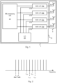
- Fig. 1 is a block diagram of a radio apparatus 1.
- the radio apparatus is considered to be a base station for a cellular communications system.
- base stations for future 5G cellular communications systems are considered.
- these examples should not be construed as limiting.
- the radio apparatus 1 comprises an antenna array 5 comprising a plurality of antenna elements 5a-d.
- the radio apparatus 1 comprises an antenna array 5 comprising a plurality of antenna elements 5a-d.
- antenna array 5 comprising a plurality of antenna elements 5a-d.
- only four antenna elements 5a-d are depicted for simplicity.
- the number of antenna elements may be much larger, such as several tens of antenna elements, or even over a hundred antenna elements.
- the radio apparatus 1 depicted in Fig. 1 comprises a communication circuit 10.
- the communication circuit 10 may be a transmitter circuit, a receiver circuit, or a transceiver circuit, and the term communication circuit is intended to generically encompass all these alternatives.
- the communication circuit 10 is configured to communicate, i.e. transmit or receive, at a carrier frequency via the multiple antenna elements 5a-d of the radio apparatus 1, e.g. in accordance with a beamforming scheme, a multiple-input multiple-output (MIMO) scheme, or some other multi-antenna transmission or reception technique.
- the communication circuit 1 comprises a plurality of radio units 15a-d.
- the radio units 15a-d may be transmitter units or receiver units.
- Each radio unit 15a-d is arranged to be connected to a separate antenna element 5a-d.
- the radio unit 15a is connected to the antenna element 5a
- the radio unit 15b is connected to the antenna element 5b
- the radio unit 15c is connected to the antenna element 5c
- the radio unit 15d is connected to the antenna element 5d.
- the communication circuit 10 comprises a local oscillator (LO) signal generation unit 20 arranged to generate a plurality of LO signals LOa-d.
- the LO signal generation unit 20 may e.g. comprise a plurality of phase-locked loops (PLLs), or other type of synthesizers, each responsible for generating one of the LO signals.
- PLLs phase-locked loops
- the LO signal generation unit is configured to supply a unique LO signal of the plurality of LO signals LOa-d to each radio unit of the plurality of radio units.
- the LO signal LOa is supplied to the radio unit 15a
- the LO signal LOb is supplied to the radio unit 15b
- the LO signal LOc is supplied to the radio unit 15c
- the LO signal LOd is supplied to the radio unit 15d.
- the communication circuit 10 illustrated in Fig. 1 further comprises a baseband processing unit 25 configured to perform baseband processing tasks on signals received and/or to be transmitted.
- the LO signal generation unit is configured to generate the plurality of LO signals LOa-d at distinct frequencies f LOa - f LOd .
- the communication circuit 10 is configured to be used in a radio communications system having an associated frequency grid with a grid spacing d, wherein the spacing between any two of the distinct frequencies f LOa - f LOd is an integer multiple of the grid spacing d.
- an LTE system utilizes orthogonal frequency-division multiplexing (OFDM) signals, using a number of equally spaced sub carriers.
- OFDM orthogonal frequency-division multiplexing
- the grid spacing d is a frequency distance between two adjacent OFDM subcarriers. This is illustrated in Fig. 2 , illustrating an OFDM signal (in the frequency domain) with a number of sub carriers separated a distance d apart.
- FIG. 2 also illustrates how the frequencies f LOa - f LOd can be selected to coincide with the sub carrier frequencies (at RF), whereby the spacing between any two of the distinct frequencies f LOa - f LOd is an integer multiple of the grid spacing d.
- Such a frequency selection also ensures that the frequency grid of the OFDM symbol is aligned with DC, or 0 Hz, at baseband, which simplifies baseband processing.
- adjacent LO frequencies are only separated by a single d. However, any integer multiple of d may be used in other applications.
- the communication circuit 10 may well comprise one or more additional pluralities of radio units, in addition to the radio units 15a-d. Such additional pluralities of radio units may reuse the same LO signals as the radio units 15a-d.
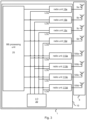
- FIG. 3 showing an embodiment of the radio apparatus 1, wherein the communication circuit 10 comprises an additional plurality of radio units 115a-d.
- the antenna array 5 comprises an additional plurality of antenna elements 105a-d. In Fig. 3 , only four antenna elements 105a-d in said additional plurality of antenna elements are depicted for simplicity. However, in practice, the number of antenna elements in said additional plurality of antenna elements may be much larger, such as several tens of antenna elements, or even over a hundred antenna elements.
- each radio unit 115a-d is arranged to be connected to a separate antenna element 105a-d.
- the radio unit 115a is connected to the antenna element 105a
- the radio unit 115b is connected to the antenna element 105b
- the radio unit 115c is connected to the antenna element 105c
- the radio unit 115d is connected to the antenna element 105d.
- the radio units 115a-d reuse the LO signals LOa-d provided to the radio units 15a-d.
- the LO signal LOa is supplied to the radio unit 115a
- the LO signal LOb is supplied to the radio unit 115b
- the LO signal LOc is supplied to the radio unit 115c
- the LO signal LOd is supplied to the radio unit 115d.
- the communication circuit 10 may in some embodiments be integrated into a single integrated circuit. In other embodiments, the communication circuit 10 may be partitioned into a number of integrated circuits. This can be particularly advantageous if the number of antenna elements in the antenna array 5 is relatively large, but also in cases with fewer antenna elements if the interspacing between the antenna elements is relatively large. A large number of antenna elements means a large number of radio units, which can make it difficult to integrate all of them into the same integrated circuit.
- the radio units 15a-d (and 115a-d) are physically close to the antenna elements 5a-d (and 105a-d) to which they are electrically connected, which is facilitated by partitioning the communication circuit 10 into multiple integrated circuits with one or more radio unit 15a-d (and 115a-d) in each.
- the LO signal generation unit 20 may be distributed over several integrated circuits as well.
- a synthesizer, such as a PLL, of the LO signal generation unit 20 may be integrated into the same integrated circuit as the radio unit or radio units that it supplies with an LO signal, or into an integrated circuit that is place physically close thereto, e.g. in the same package or on the same printed circuit board.
- each of the radio units 15a-d is implemented on a separate integrated circuit.
- the integrated circuit comprising the radio unit 15a may comprise a synthesizer of the LO signal generation unit 20 that generates the LO signal LOa
- the integrated circuit comprising the radio unit 15b may comprise a synthesizer of the LO signal generation unit 20 that generates the LO signal LOb
- the integrated circuit comprising the radio unit 15c may comprise a synthesizer of the LO signal generation unit 20 that generates the LO signal LOc
- the integrated circuit comprising the radio unit 15a may comprise a synthesizer of the LO signal generation unit 20 that generates the LO signal LOd.
- the integrated circuit comprising the radio unit 15a may additionally comprise the radio unit 115a
- the integrated circuit comprising the radio unit 15b may additionally comprise the radio unit 115b
- the integrated circuit comprising the radio unit 15c may additionally comprise the radio unit 115c
- the integrated circuit comprising the radio unit 15d may additionally comprise the radio unit 115d.
- the radio unit 15a is located together with a PLL (or other type of synthesizer) 120a, which is configured to generate the LO signal LOa, in an integrated circuit 140a.
- the radio unit 115a may be integrated in the same integrated circuit 140a.
- the radio unit 15b is located together with a PLL (or other type of synthesizer) 120b, which is configured to generate the LO signal LOb, in an integrated circuit 140b.
- the radio unit 115b may be integrated in the same integrated circuit 140b. In the same way, in Fig.
- the radio unit 15c is located together with a PLL (or other type of synthesizer) 120c, which is configured to generate the LO signal LOc, in an integrated circuit 140c.
- the radio unit 115c may be integrated in the same integrated circuit 140c.
- the radio unit 15d is located together with a PLL (or other type of synthesizer) 120d, which is configured to generate the LO signal LOd, in an integrated circuit 140d.
- the radio unit 115d may be integrated in the same integrated circuit 140d.
- the PLLs 120a-d are driven by a common reference oscillator, such as a crystal oscillator, 130.
- the PLLs 120a-d and the reference oscillator 130 are comprised in the LO signal generation unit 20 ( Figs. 1 and 3 ).
- the integrated circuits 140a-d mentioned above are below referred to as RF-ASICs 140a-d.
- the RF-ASICs 140a-d are placed physically close to the respective antennas 5a-d (and optionally the antennas 105a-d).
- reference signs 140a-d may represent entities of a plurality of integrated circuits that are located close to each other, such as in the same integrated circuit package.
- the baseband processing unit 25 may be integrated into a single integrated circuit, or may be distributed over multiple integrated circuits.
- the radio units 15a-d are receiver units.
- the LO signals LOa-d are supplied to down-conversion mixers of the respective receiver units 15a-d.
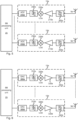
- a block diagram in Fig. 5 showing part of the radio apparatus 1 according to an embodiment.
- a brief description of the receiver unit 15a according to the embodiment illustrated in Fig. 5 , is provided.
- Design of radio receivers in general is well known in the art, and therefore not described in great detail herein.
- the receiver unit 15a comprises an RF filter 200a connected to the antenna 5a.
- the receiver unit 15a in Fig. 5 further comprises an amplifier 210a, such as a low-noise amplifier (LNA), connected to the RF filter 200a.
- the receiver unit 15a in Fig. 5 comprises a down-conversion mixer 220a, configured to down convert the RF signal output from the amplifier 210a to a baseband signal.
- the LO signal LOa is supplied to the down-conversion mixer 220a.
- the receiver unit 15a comprises a baseband filter 230a configured to suppress noise and other unwanted signal components outside of the signal band of the baseband signal, followed by an analog-to-digital converter 240a configured to convert the filtered baseband signal into a digital representation.
- the baseband processing unit 25 is configured to receive the baseband output signals from the receiver units 15a-d, e.g. the digital baseband output signals generated by the ADCs 240a-240d ( Fig. 5 ). These baseband signals are not aligned with each other in frequency, due to the use of different LO frequencies. Therefore, the baseband processing unit 25 is configured to frequency align the baseband output signals, to facilitate further signal processing. In, for example, OFDM applications, such frequency alignment can be advantageously performed in the frequency domain.
- the digital baseband signals from the ADCs 240a-d can be transformed to the frequency domain, e.g. using a discrete Fourier transform (DFT), which may e.g. be implemented as a fast Fourier transform (FFT).
- DFT discrete Fourier transform
- FFT fast Fourier transform
- the resulting frequency-domain signals can then be aligned by simply shifting the signals either up or down in frequency such that sub carriers, or "FFT bins", that correspond to the same subcarrier frequency appear in the same position in the frequency-shifted frequency-domain signals.
- the frequency alignment can also be performed in the time domain by multiplication with a sampled version of e j ⁇ t , where j denotes the imaginary unit ( ⁇ 1 ), ⁇ is an angular frequency corresponding to the frequency shift to be achieved, and t denotes time.
- the receiver units say 15a, implemented as a direct conversion receiver in an OFDM application. If the LO signal is placed on the frequency grid for the OFDM signal, then the DC-offset from the direct conversion receiver 15a will only affect one FFT bin. By averaging the bin at DC over a number of consecutive OFDM symbols, it will be possible to suppress the DC-offset after a certain time, e.g. after number of slots, wherein a slot corresponds to a number of consecutive OFDM symbols. During this time, the FFT bin at DC could be ignored for the particular receiver unit 15a, since data is received on the subcarrier corresponding to that bin also in the other receiver units 15b-d, which have used LO frequencies, that could be used for decoding of this specific subcarrier. The time needed until all FFT bins could be used again will e.g. depend on the modulation, which requires a certain signal-to-noise ratio (SNR) for successful de-coding.
- SNR signal-to-noise ratio
- the baseband processing unit 25 is further configured to recombine the frequency-aligned baseband output signals that are the result of the frequency alignment.
- the recombining can be performed in the same way as if the same LO frequency had been used, and is therefore not described in any greater detail herein. Exactly how the signals are recombined depends on how the radio apparatus 1 is configured, and can e.g. be according to a beamforming scheme, multiple-input multiple-output (MIMO) scheme, or any other multi-antenna receiver scheme.
- MIMO multiple-input multiple-output
- the LO signals LOa-d may be supplied to up-conversion mixers of the respective transmitter units 15a-d.
- a block diagram in Fig. 6 showing part of the radio apparatus 1 according to an example where the radio units 15a-d are transmitter units 15a-d.
- a brief description of the transmitter unit 15a according to the example illustrated in Fig. 6 , is provided.
- the transmitter unit 15a comprises a digital-to-analog converter (DAC) 300a, configured to convert a digital input signal of the transmitter unit 15a to the analog domain.
- the transmitter unit 15a depicted in Fig. 6 further comprises a reconstruction filter 31 0a, configured to suppress spectral replicas and other unwanted signal content outside of the signal band of the output signal of the DAC 300a.
- the transmitter unit 15a comprises an up-conversion mixer 320a configured to up convert the output signal from the reconstruction filter 310a to an RF signal.
- the transmitter unit 15a comprises an amplifier 330a, such as a power amplifier (PA), configured to feed the RF signal from the up-conversion mixer 320a to the antenna 5a via an RF filter 340a of the transmitter unit 15a.
- PA power amplifier
- the baseband processing unit 25 is configured to generate input signals to the transmitter units 15a-d. Due to that the frequencies of the LO signals LOa-d are different, the input signals to the transmitter units should be frequency shifted the same amount, but in the opposite direction, such that signals transmitted via the antennas end up at the correct RF frequency. Accordingly, in some examples, the baseband processing unit 25 is configured to generate baseband transmit signals. This can be done in the same way as if all LO signals were using the same LO frequency, e.g. in accordance with a beamforming scheme or a MIMO scheme. Furthermore, the baseband processing unit 25 may be configured to frequency shift the baseband transmit signals to account for the distinct LO frequencies f LOa - f LOd .
- such frequency shifting can be advantageously performed in the frequency domain.
- the frequency shifting can be performed simply shifting the signals either up or down in frequency.
- the frequency-domain representation of the frequency-shifted baseband transmit signals can then be transformed into a time-domain representation, e.g. using an IFFT.
- the frequency shift can be performed in the time domain by multiplication with a sampled version of e j ⁇ t .
- the baseband processing unit 25 may further be configured to supply the frequency-shifted baseband transmit signals to the transmitter units 15a-d as the above-mentioned input signals.
- the block diagrams in Figs. 5 and 6 illustrating embodiments of receiver units 15a-d and examples of transmitter units 15a-d are only examples.
- the down-conversion mixer 220a and up-conversion mixer 320a are illustrated in Figs. 5 and 6 as single mixers.
- they may be implemented as quadrature mixers, comprising a mixer for an in-phase (I) signal path and a mixer for a quadrature-phase (Q) signal path.
- the LO signal LOa is a quadrature LO signal having I and a Q component with a mutual 90-degree phase difference.
- the design of quadrature transmitters and receivers is well known in the art and not further described herein.
- other combinations of components, such as mixers, filters, and amplifiers, than those illustrated in Figs. 5-6 may be used as well, while still benefitting from using distinct LO frequencies for different LO signals LOa-d.
- embodiments have been described, e.g. with reference to Fig. 5 , comprising receiver units.
- examples, which are not claimed per se have been described, e.g. with reference to Fig. 6 , comprising transmitter units.
- the communication circuit 10 which is a transceiver circuit, comprising both a plurality of transmitter units operating at distinct LO frequencies (e.g. as in Fig. 6 ), and a plurality of receiver units operating at distinct LO frequencies (e.g. as in Fig. 5 ) as defined in claim 1, which may or may not be the same distinct LO frequencies as for the transmitter units.
- the radio apparatus 1 is a cellular base station configured to operate in a 3GPP band that starts at 4.5 GHz and ends at 4.9 GHz.
- the antenna array comprises 64 antenna elements.
- the communication circuit 10 comprises 32 RF application specific integrated circuits (ASICs). Each RF ASIC comprises two receiver units and two transmitter units that share the same LO signal, generated by a PLL comprised in the same RF ASIC. The LO frequencies used in the different are generated in increments of 1.005 MHz.
- the supported radio BW needs to be expanded in order to support the staggering of the LO frequency between different RF ASICs.
- it will mean an expansion of the bandwidth (BW) with a factor 400 + 16 + 15 1.005 400 ⁇ 1.078
- the offset is only one OFDM subcarrier distance.
- LTE that is 15kHz
- other distances may be used in future 5G systems, perhaps 75 kHz.
- the BW increase would be so small that it can be seen as negligible, or almost none.
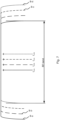
- the BW increase described above is illustrated in Fig. 7 .
- the LO signals LOa-d are illustrated as arrows located at the respective LO frequencies f LOa -f LOd .
- the radio unit 15a has an operational band B-a, in which it is capable of operating, in the RF domain centered at f LOa .
- the radio unit 15b has an operational band B-b, in which it is capable of operating, in the RF domain centered at f LOb .
- the radio unit 15c has an operational band B-c, in which it is capable of operating, in the RF domain centered at f LOc .
- the radio unit 15d has an operational band B-d, in which it is capable of operating, in the RF domain centered at f LOd .
- the radio units 15a-d are assumed to be identically designed and merely differ in terms of the LO frequency used. In particular, the bandwidth of the bands B-a, B-b, B-c, and B-d, are assumed to be the same.
- Fig. 7 also shows an RF band, such as a 3GPP band, in which the radio apparatus 1 is to operate in.
- the bandwidth of the bands B-a, B-b, B-c, and B-d need to be slightly higher than the bandwidth if the RF band itself, as can be seen from Fig. 7 .
- the method may comprise the step 400 of generating the above-mentioned plurality of LO signals LOa-d at distinct frequencies f LOa - f LOd . Furthermore, as also illustrated in Fig. 8 , the method may comprise the step 410 of supplying a unique LO signal LOa-d of the plurality of LO signals LOa-d to each radio unit 15a-d of the plurality of radio units 15a-d. Reference signs 405 and 415 are inserted at nodes of the flowchart in Fig. 8 , to illustrate how it connects with the flowcharts in Figs. 9-12 .
- the radio units 15a-d are receiver units 15a-d.
- the step 410 of supplying the LO signals LOa-d to the receiver units 15a-d may comprise a step 410a of supplying the LO signals LOa-d to down-conversion mixers, such as 220a-d in Fig. 5 , of the receiver units 15a-d, as illustrated in Fig. 9 .
- the method further comprises step 420 receiving, e.g. by the baseband processing unit 25, baseband output signals from the receiver units 15a-d. Moreover, the method comprises step 430 of frequency aligning, e.g. by the baseband processing unit 25, the baseband output signals. The method also comprises step 440 of recombining, e.g. by the baseband processing unit 25, the frequency-aligned baseband output signals.
- step 410 of supplying the LO signals LOa-d to the transmitter units 15a-d may comprise a step 410b of supplying the LO signals LOa-d to up-conversion mixers, such as 320a-d in Fig. 6 , of the transmitter units 15a-d, as illustrated in Fig. 11 .
- the method may further comprise step 450 of generating, e.g. by the baseband processing unit 25, baseband transmit signals. Moreover, the method may comprise step 460 of frequency shifting, e.g. by the baseband processing unit 25, the baseband transmit signals to account for the distinct LO frequencies. The method may also comprise step 470 of supplying, e.g. by the baseband processing unit 25, the frequency-shifted baseband transmit signals to the transmitter units 15a-d.
Landscapes
- Engineering & Computer Science (AREA)
- Signal Processing (AREA)
- Computer Networks & Wireless Communication (AREA)
- Transceivers (AREA)
Description
- The present invention relates to multi-antenna radio communication.
- Fifth generation (5G) cellular systems will initially be deployed on higher frequencies and with higher carrier bandwidths, then existing state of the art cellular systems, such as fourth generation (4G) cellular systems. One development in cellular communications, leading towards the development of 5G systems, is an increase of the number of antenna elements used especially in base stations. This increase in the number of antenna elements enables efficient multiple-input multiple-output (MIMO) and beamforming schemes to be used. 5G systems are, at least initially, foreseen to be deployed on higher frequencies and with higher carrier bandwidths, than, for instance, 4G cellular systems. The use of an antenna array system (AAS) with multiple antenna elements help overcome the increased path loss between the base station and user equipment (UE) due to the higher frequency. For example, an antenna array with 64 antenna elements can give signal-to-noise ratio (SNR) gain of 10 log10 64 = 18 dB, compared with using a single antenna.
- Hence, the increased number of antenna elements provides advantages. However, it also poses challenges in terms of hardware design. A straightforward design approach is to use equally configured transmit and receive paths for all antenna elements, which provides for a simple and modular design.
- Documents
US2013051284 ,US2014269853 andEP2299774 all disclose a communication circuit for communication at a carrier frequency via multiple antenna elements and further comprising a local oscillator signal generation unit generating a plurality of local oscillator signals at distinct frequencies. - The inventor has realized that using equally configured transmit and receive paths for all antenna elements can results in a number of imperfections being added in a correlated way, resulting in an overall reduced gain from using multiple antennas. The inventor has further realized that by operating transmitters or receivers connected to different antenna elements at different local oscillator (LO) frequencies, even though they communicate at the same radio frequency (RF) carrier frequency, such problems can be reduced.
- According to a first aspect, there is provided a communication circuit according to
claim 1. - According to a second aspect, there is provided a method according to
claim 5. - Further embodiments are defined in the dependent claims. It should be emphasized that the term "comprises/comprising" when used in this specification is taken to specify the presence of stated features, integers, steps, or components, but does not preclude the presence or addition of one or more other features, integers, steps, components, or groups thereof.
- Further objects, features and advantages of embodiments of the invention will appear from the following detailed description, reference being made to the accompanying drawings, in which:
-
Fig. 1 is a block diagram of a radio apparatus; -
Fig. 2 illustrates subcarriers, subcarrier spacing, and LO frequencies; -
Figs. 3-4 are block diagrams of a radio apparatus; -
Fig. 5 is a block diagram of part of a radio apparatus with receiver units; -
Fig. 6 is a block diagram of part of a radio apparatus with transmitter units; -
Fig. 7 illustrates bandwidths of radio units; and -
Figs. 8-12 are flowcharts for methods of operating a radio apparatus. -
Fig. 1 is a block diagram of aradio apparatus 1. As an example throughout this disclosure, the radio apparatus is considered to be a base station for a cellular communications system. In particular, base stations for future 5G cellular communications systems are considered. However, these examples should not be construed as limiting. - In
Fig. 1 , theradio apparatus 1 comprises anantenna array 5 comprising a plurality ofantenna elements 5a-d. InFig. 1 , only fourantenna elements 5a-d are depicted for simplicity. However, in practice, the number of antenna elements may be much larger, such as several tens of antenna elements, or even over a hundred antenna elements. - Furthermore, the
radio apparatus 1 depicted inFig. 1 comprises acommunication circuit 10. Thecommunication circuit 10 may be a transmitter circuit, a receiver circuit, or a transceiver circuit, and the term communication circuit is intended to generically encompass all these alternatives. Thecommunication circuit 10 is configured to communicate, i.e. transmit or receive, at a carrier frequency via themultiple antenna elements 5a-d of theradio apparatus 1, e.g. in accordance with a beamforming scheme, a multiple-input multiple-output (MIMO) scheme, or some other multi-antenna transmission or reception technique. Thecommunication circuit 1 comprises a plurality ofradio units 15a-d. Theradio units 15a-d may be transmitter units or receiver units. Eachradio unit 15a-d is arranged to be connected to aseparate antenna element 5a-d. InFig. 1 , theradio unit 15a is connected to theantenna element 5a, theradio unit 15b is connected to theantenna element 5b, theradio unit 15c is connected to theantenna element 5c, and theradio unit 15d is connected to theantenna element 5d. Furthermore, thecommunication circuit 10 comprises a local oscillator (LO)signal generation unit 20 arranged to generate a plurality of LO signals LOa-d. The LOsignal generation unit 20 may e.g. comprise a plurality of phase-locked loops (PLLs), or other type of synthesizers,, each responsible for generating one of the LO signals. Furthermore, the LO signal generation unit is configured to supply a unique LO signal of the plurality of LO signals LOa-d to each radio unit of the plurality of radio units. For simple notation, the LO signal LOa is supplied to theradio unit 15a, the LO signal LOb is supplied to theradio unit 15b, the LO signal LOc is supplied to theradio unit 15c, and the LO signal LOd is supplied to theradio unit 15d. - The
communication circuit 10 illustrated inFig. 1 further comprises abaseband processing unit 25 configured to perform baseband processing tasks on signals received and/or to be transmitted. - Assume for a moment, as a reference example, that all of the LO signals LOa-d have the same frequency, which would be a straightforward and natural choice. The inventor has realized that there are a number of problems with such a selection of frequency. The terminology used in some of the example presented below assumes that a third generation partnership program (3GPP) long-term evolution (LTE) system, or LTE-like system, is used. For example:
- 1) Transmitter LO-leakage (in case the
radio units 15a-d are transmitter units): The LO-leakage from each transmitter unit will add in phase for a specific direction from the antenna array. Furthermore all LO-leakage energy will be concentrated on the same frequency, which will make the decoding in the UE of the information on that frequency challenging. - 2) Receiver flicker noise (in case the
radio units 15a-d are receiver units, direct conversion assumed): The RB:s (resource blocks) close to DC (after downconversion) will be affected by an increased NF (noise figure) due to flicker noise. If the same LO-frequency is used, then the degradation will be concentrated on the frequency range close to the used LO-frequency. This will especially be cumbersome if a relatively narrow frequency band is used, such as envisioned for some type of machine-type communication (MTC). - 3) Receiver DC offset change due to AGC activity (in case the
radio units 15a-d are receiver units, direct conversion assumed): The RB:s close to DC (after downconversion) will be affected by the DC-offset. The distortion will be added up, if the same LO frequency is used. The impact on system performance could be relatively high, e.g. if a reference signal, or pilot signal, is damaged. - 4) Spurious response (in case the
radio units 15a-d are receiver units). Due to spurious frequency components in the LO signals, e.g. due to leakage of other LO signals on the same integrated circuit chip, unwanted signal components will be down-converted to the same band as the wanted signal components and interfere with the wanted signal components, which is referred to as spurious response. The affected RB:s, being blocked by interfering signals, due to spurious response will be correlated between the different receiver units. - 5) Spurious emission (in case the
radio units 15a-d are transmitter units): Any (out of band) spurious emission related to TX LO-frequency, e.g. caused by unintentional mixing of the TX LO with some other clock signal due to leakage, will end up at same frequency for all radio units and add up in the air. This in turn could lead non-compliance with out-of band spectral emission requirements. - The inventor has realized that such problems can be reduced by operating different radio units at different LO frequencies. Hence, in accordance with some embodiments, the LO signal generation unit is configured to generate the plurality of LO signals LOa-d at distinct frequencies f LOa-f LOd.
- According to the claims, the
communication circuit 10 is configured to be used in a radio communications system having an associated frequency grid with a grid spacing d, wherein the spacing between any two of the distinct frequencies f LOa-f LOd is an integer multiple of the grid spacing d. For example, an LTE system utilizes orthogonal frequency-division multiplexing (OFDM) signals, using a number of equally spaced sub carriers. In such a case, there is a frequency grid defined by the frequency positions of the sub carriers. The grid spacing d is a frequency distance between two adjacent OFDM subcarriers. This is illustrated inFig. 2 , illustrating an OFDM signal (in the frequency domain) with a number of sub carriers separated a distance d apart.Fig. 2 also illustrates how the frequencies f LOa-f LOd can be selected to coincide with the sub carrier frequencies (at RF), whereby the spacing between any two of the distinct frequencies f LOa-f LOd is an integer multiple of the grid spacing d. Such a frequency selection also ensures that the frequency grid of the OFDM symbol is aligned with DC, or 0 Hz, at baseband, which simplifies baseband processing. InFig. 2 , adjacent LO frequencies are only separated by a single d. However, any integer multiple of d may be used in other applications. - It should be noted that the
communication circuit 10 may well comprise one or more additional pluralities of radio units, in addition to theradio units 15a-d. Such additional pluralities of radio units may reuse the same LO signals as theradio units 15a-d. This is illustrated inFig. 3 , showing an embodiment of theradio apparatus 1, wherein thecommunication circuit 10 comprises an additional plurality ofradio units 115a-d. Furthermore, inFig. 3 , theantenna array 5 comprises an additional plurality ofantenna elements 105a-d. InFig. 3 , only fourantenna elements 105a-d in said additional plurality of antenna elements are depicted for simplicity. However, in practice, the number of antenna elements in said additional plurality of antenna elements may be much larger, such as several tens of antenna elements, or even over a hundred antenna elements. - In the embodiment illustrated in
Fig. 3 , eachradio unit 115a-d is arranged to be connected to aseparate antenna element 105a-d. InFig. 3 , theradio unit 115a is connected to theantenna element 105a, theradio unit 115b is connected to theantenna element 105b, theradio unit 115c is connected to theantenna element 105c, and theradio unit 115d is connected to theantenna element 105d. Furthermore, inFig. 3 , theradio units 115a-d reuse the LO signals LOa-d provided to theradio units 15a-d. The LO signal LOa is supplied to theradio unit 115a, the LO signal LOb is supplied to theradio unit 115b, the LO signal LOc is supplied to theradio unit 115c, and the LO signal LOd is supplied to theradio unit 115d. - The
communication circuit 10 may in some embodiments be integrated into a single integrated circuit. In other embodiments, thecommunication circuit 10 may be partitioned into a number of integrated circuits. This can be particularly advantageous if the number of antenna elements in theantenna array 5 is relatively large, but also in cases with fewer antenna elements if the interspacing between the antenna elements is relatively large. A large number of antenna elements means a large number of radio units, which can make it difficult to integrate all of them into the same integrated circuit. Furthermore, it is generally advantageous to keep theradio units 15a-d (and 115a-d) physically close to theantenna elements 5a-d (and 105a-d) to which they are electrically connected, which is facilitated by partitioning thecommunication circuit 10 into multiple integrated circuits with one ormore radio unit 15a-d (and 115a-d) in each. Furthermore, the LOsignal generation unit 20 may be distributed over several integrated circuits as well. For example, a synthesizer, such as a PLL, of the LOsignal generation unit 20 may be integrated into the same integrated circuit as the radio unit or radio units that it supplies with an LO signal, or into an integrated circuit that is place physically close thereto, e.g. in the same package or on the same printed circuit board. For instance, in some embodiments, each of theradio units 15a-d is implemented on a separate integrated circuit. With reference toFigs. 1 and3 , the integrated circuit comprising theradio unit 15a may comprise a synthesizer of the LOsignal generation unit 20 that generates the LO signal LOa, the integrated circuit comprising theradio unit 15b may comprise a synthesizer of the LOsignal generation unit 20 that generates the LO signal LOb, the integrated circuit comprising theradio unit 15c may comprise a synthesizer of the LOsignal generation unit 20 that generates the LO signal LOc, and the integrated circuit comprising theradio unit 15a may comprise a synthesizer of the LOsignal generation unit 20 that generates the LO signal LOd. With reference toFig. 3 , the integrated circuit comprising theradio unit 15a may additionally comprise theradio unit 115a, the integrated circuit comprising theradio unit 15b may additionally comprise theradio unit 115b, the integrated circuit comprising theradio unit 15c may additionally comprise theradio unit 115c, and the integrated circuit comprising theradio unit 15d may additionally comprise theradio unit 115d. - The partitioning discussed above is illustrated in
Fig. 4 . InFig. 4 , theradio unit 15a is located together with a PLL (or other type of synthesizer) 120a, which is configured to generate the LO signal LOa, in anintegrated circuit 140a. Optionally, theradio unit 115a may be integrated in the sameintegrated circuit 140a. Similarly, inFig. 4 , theradio unit 15b is located together with a PLL (or other type of synthesizer) 120b, which is configured to generate the LO signal LOb, in an integrated circuit 140b. Optionally, theradio unit 115b may be integrated in the same integrated circuit 140b. In the same way, inFig. 4 , theradio unit 15c is located together with a PLL (or other type of synthesizer) 120c, which is configured to generate the LO signal LOc, in anintegrated circuit 140c. Optionally, theradio unit 115c may be integrated in the sameintegrated circuit 140c. Also, inFig. 4 , theradio unit 15d is located together with a PLL (or other type of synthesizer) 120d, which is configured to generate the LO signal LOd, in anintegrated circuit 140d. Optionally, theradio unit 115d may be integrated in the sameintegrated circuit 140d. ThePLLs 120a-d are driven by a common reference oscillator, such as a crystal oscillator, 130. ThePLLs 120a-d and thereference oscillator 130 are comprised in the LO signal generation unit 20 (Figs. 1 and3 ). Theintegrated circuits 140a-d mentioned above are below referred to as RF-ASICs 140a-d. The RF-ASICs 140a-d are placed physically close to therespective antennas 5a-d (and optionally theantennas 105a-d). In alternative embodiments,reference signs 140a-d may represent entities of a plurality of integrated circuits that are located close to each other, such as in the same integrated circuit package. - In a similar way, the
baseband processing unit 25 may be integrated into a single integrated circuit, or may be distributed over multiple integrated circuits. - According to the claims, the
radio units 15a-d are receiver units. The LO signals LOa-d are supplied to down-conversion mixers of therespective receiver units 15a-d. This is illustrated with a block diagram inFig. 5 showing part of theradio apparatus 1 according to an embodiment. In the following, a brief description of thereceiver unit 15a, according to the embodiment illustrated inFig. 5 , is provided. The same description holds for thereceiver units 15b-d by simply replacing "a" with "b", "c", or "d". Design of radio receivers in general is well known in the art, and therefore not described in great detail herein. InFig. 5 , thereceiver unit 15a comprises anRF filter 200a connected to theantenna 5a. Thereceiver unit 15a inFig. 5 further comprises anamplifier 210a, such as a low-noise amplifier (LNA), connected to theRF filter 200a. Furthermore, thereceiver unit 15a inFig. 5 comprises a down-conversion mixer 220a, configured to down convert the RF signal output from theamplifier 210a to a baseband signal. The LO signal LOa is supplied to the down-conversion mixer 220a. - In
Fig. 5 , thereceiver unit 15a comprises abaseband filter 230a configured to suppress noise and other unwanted signal components outside of the signal band of the baseband signal, followed by an analog-to-digital converter 240a configured to convert the filtered baseband signal into a digital representation. - The
baseband processing unit 25 is configured to receive the baseband output signals from thereceiver units 15a-d, e.g. the digital baseband output signals generated by theADCs 240a-240d (Fig. 5 ). These baseband signals are not aligned with each other in frequency, due to the use of different LO frequencies. Therefore, thebaseband processing unit 25 is configured to frequency align the baseband output signals, to facilitate further signal processing. In, for example, OFDM applications, such frequency alignment can be advantageously performed in the frequency domain. The digital baseband signals from theADCs 240a-d can be transformed to the frequency domain, e.g. using a discrete Fourier transform (DFT), which may e.g. be implemented as a fast Fourier transform (FFT). The resulting frequency-domain signals can then be aligned by simply shifting the signals either up or down in frequency such that sub carriers, or "FFT bins", that correspond to the same subcarrier frequency appear in the same position in the frequency-shifted frequency-domain signals. The frequency alignment can also be performed in the time domain by multiplication with a sampled version of ejωt, where j denotes the imaginary unit (
- Consider one of the receiver units, say 15a, implemented as a direct conversion receiver in an OFDM application. If the LO signal is placed on the frequency grid for the OFDM signal, then the DC-offset from the
direct conversion receiver 15a will only affect one FFT bin. By averaging the bin at DC over a number of consecutive OFDM symbols, it will be possible to suppress the DC-offset after a certain time, e.g. after number of slots, wherein a slot corresponds to a number of consecutive OFDM symbols. During this time, the FFT bin at DC could be ignored for theparticular receiver unit 15a, since data is received on the subcarrier corresponding to that bin also in theother receiver units 15b-d, which have used LO frequencies, that could be used for decoding of this specific subcarrier. The time needed until all FFT bins could be used again will e.g. depend on the modulation, which requires a certain signal-to-noise ratio (SNR) for successful de-coding. - The
baseband processing unit 25 is further configured to recombine the frequency-aligned baseband output signals that are the result of the frequency alignment. The recombining can be performed in the same way as if the same LO frequency had been used, and is therefore not described in any greater detail herein. Exactly how the signals are recombined depends on how theradio apparatus 1 is configured, and can e.g. be according to a beamforming scheme, multiple-input multiple-output (MIMO) scheme, or any other multi-antenna receiver scheme. - A similar technique can be applied to
radio units 15a-d in the form oftransmitter units 15a-d. This is not claimed per se, but examples are provided which may be combined with the claimed subject matter as described below. In such examples, the LO signals LOa-d may be supplied to up-conversion mixers of therespective transmitter units 15a-d. This is illustrated with a block diagram inFig. 6 showing part of theradio apparatus 1 according to an example where theradio units 15a-d aretransmitter units 15a-d. In the following, a brief description of thetransmitter unit 15a, according to the example illustrated inFig. 6 , is provided. The same description holds for thetransmitter units 15b-d by simply replacing "a" with "b", "c", or "d". Design of radio transmitters in general is well known in the art, and therefore not described in great detail herein. InFig. 6 , thetransmitter unit 15a comprises a digital-to-analog converter (DAC) 300a, configured to convert a digital input signal of thetransmitter unit 15a to the analog domain. Thetransmitter unit 15a depicted inFig. 6 further comprises a reconstruction filter 31 0a, configured to suppress spectral replicas and other unwanted signal content outside of the signal band of the output signal of theDAC 300a. Furthermore, inFig. 6 , thetransmitter unit 15a comprises an up-conversion mixer 320a configured to up convert the output signal from thereconstruction filter 310a to an RF signal. Moreover, inFig. 6 , thetransmitter unit 15a comprises anamplifier 330a, such as a power amplifier (PA), configured to feed the RF signal from the up-conversion mixer 320a to theantenna 5a via anRF filter 340a of thetransmitter unit 15a. - The
baseband processing unit 25 is configured to generate input signals to thetransmitter units 15a-d. Due to that the frequencies of the LO signals LOa-d are different, the input signals to the transmitter units should be frequency shifted the same amount, but in the opposite direction, such that signals transmitted via the antennas end up at the correct RF frequency. Accordingly, in some examples, thebaseband processing unit 25 is configured to generate baseband transmit signals. This can be done in the same way as if all LO signals were using the same LO frequency, e.g. in accordance with a beamforming scheme or a MIMO scheme. Furthermore, thebaseband processing unit 25 may be configured to frequency shift the baseband transmit signals to account for the distinct LO frequencies fLOa - fLOd. In, for example, OFDM applications, such frequency shifting can be advantageously performed in the frequency domain. For instance, if the baseband transmit signals are represented in the frequency domain by means of a DFT or FFT, the frequency shifting can be performed simply shifting the signals either up or down in frequency. The frequency-domain representation of the frequency-shifted baseband transmit signals can then be transformed into a time-domain representation, e.g. using an IFFT. Alternatively, as for the frequency alignment discussed above, the frequency shift can be performed in the time domain by multiplication with a sampled version of ejωt . Thebaseband processing unit 25 may further be configured to supply the frequency-shifted baseband transmit signals to thetransmitter units 15a-d as the above-mentioned input signals. - It should be noted that the block diagrams in
Figs. 5 and 6 illustrating embodiments ofreceiver units 15a-d and examples oftransmitter units 15a-d are only examples. For example, the down-conversion mixer 220a and up-conversion mixer 320a are illustrated inFigs. 5 and 6 as single mixers. However, in some embodiments, they may be implemented as quadrature mixers, comprising a mixer for an in-phase (I) signal path and a mixer for a quadrature-phase (Q) signal path. In such embodiments, the LO signal LOa is a quadrature LO signal having I and a Q component with a mutual 90-degree phase difference. The design of quadrature transmitters and receivers is well known in the art and not further described herein. Furthermore, other combinations of components, such as mixers, filters, and amplifiers, than those illustrated inFigs. 5-6 may be used as well, while still benefitting from using distinct LO frequencies for different LO signals LOa-d. - Above, embodiments have been described, e.g. with reference to
Fig. 5 , comprising receiver units. Furthermore, examples, which are not claimed per se, have been described, e.g. with reference toFig. 6 , comprising transmitter units. These embodiments and examples can be combined, resulting in embodiments of thecommunication circuit 10 which is a transceiver circuit, comprising both a plurality of transmitter units operating at distinct LO frequencies (e.g. as inFig. 6 ), and a plurality of receiver units operating at distinct LO frequencies (e.g. as inFig. 5 ) as defined inclaim 1, which may or may not be the same distinct LO frequencies as for the transmitter units. - According to one example, the
radio apparatus 1 is a cellular base station configured to operate in a 3GPP band that starts at 4.5 GHz and ends at 4.9 GHz. The antenna array comprises 64 antenna elements. Thecommunication circuit 10 comprises 32 RF application specific integrated circuits (ASICs). Each RF ASIC comprises two receiver units and two transmitter units that share the same LO signal, generated by a PLL comprised in the same RF ASIC. The LO frequencies used in the different are generated in increments of 1.005 MHz. The LO frequencies are given by

- Compared with a radio apparatus where all radio units operate on the same LO frequency, the supported radio BW needs to be expanded in order to support the staggering of the LO frequency between different RF ASICs. In the example above it will mean an expansion of the bandwidth (BW) with a
factor 
- A 7.8% increase in BW, which can be seen as marginal. In another example, the offset is only one OFDM subcarrier distance. In LTE, that is 15kHz, other distances may be used in future 5G systems, perhaps 75 kHz. In such an example, the BW increase would be so small that it can be seen as negligible, or almost none.
- The BW increase described above is illustrated in
Fig. 7 . InFig. 7 , the LO signals LOa-d are illustrated as arrows located at the respective LO frequencies fLOa-fLOd . Theradio unit 15a has an operational band B-a, in which it is capable of operating, in the RF domain centered at fLOa. Theradio unit 15b has an operational band B-b, in which it is capable of operating, in the RF domain centered at fLOb. Theradio unit 15c has an operational band B-c, in which it is capable of operating, in the RF domain centered at fLOc. Theradio unit 15d has an operational band B-d, in which it is capable of operating, in the RF domain centered at fLOd. Theradio units 15a-d are assumed to be identically designed and merely differ in terms of the LO frequency used. In particular, the bandwidth of the bands B-a, B-b, B-c, and B-d, are assumed to be the same.Fig. 7 also shows an RF band, such as a 3GPP band, in which theradio apparatus 1 is to operate in. In order for this RF band to be contained within each of the bands B-a, B-b, B-c, and B-d, the bandwidth of the bands B-a, B-b, B-c, and B-d need to be slightly higher than the bandwidth if the RF band itself, as can be seen fromFig. 7 . - According to some embodiments, there is provided a method of operating the
radio apparatus 1 described above. As illustrated inFig. 8 , the method may comprise thestep 400 of generating the above-mentioned plurality of LO signals LOa-d at distinct frequencies fLOa - fLOd. Furthermore, as also illustrated inFig. 8 , the method may comprise thestep 410 of supplying a unique LO signal LOa-d of the plurality of LO signals LOa-d to eachradio unit 15a-d of the plurality ofradio units 15a-d. Reference signs 405 and 415 are inserted at nodes of the flowchart inFig. 8 , to illustrate how it connects with the flowcharts inFigs. 9-12 . - In the claims, as mentioned above, the
radio units 15a-d arereceiver units 15a-d. Thestep 410 of supplying the LO signals LOa-d to thereceiver units 15a-d may comprise astep 410a of supplying the LO signals LOa-d to down-conversion mixers, such as 220a-d inFig. 5 , of thereceiver units 15a-d, as illustrated inFig. 9 . - Furthermore, as illustrated in
Fig. 10 , and in line with what is described above regarding embodiments of theradio apparatus 1 where theradio units 15a-d arereceiver units 15a-d, the method further comprises step 420 receiving, e.g. by thebaseband processing unit 25, baseband output signals from thereceiver units 15a-d. Moreover, the method comprises step 430 of frequency aligning, e.g. by thebaseband processing unit 25, the baseband output signals. The method also comprises step 440 of recombining, e.g. by thebaseband processing unit 25, the frequency-aligned baseband output signals. - In the examples mentioned above, which are not claimed per se, where the
radio units 15a-d aretransmitter units 15a-d, step 410 of supplying the LO signals LOa-d to thetransmitter units 15a-d may comprise astep 410b of supplying the LO signals LOa-d to up-conversion mixers, such as 320a-d inFig. 6 , of thetransmitter units 15a-d, as illustrated inFig. 11 . - Furthermore, as illustrated in
Fig. 12 , and in line with what is described above regarding the examples, which are not claimed per se, where theradio units 15a-d aretransmitter units 15a-d, the method may further comprisestep 450 of generating, e.g. by thebaseband processing unit 25, baseband transmit signals. Moreover, the method may comprise step 460 of frequency shifting, e.g. by thebaseband processing unit 25, the baseband transmit signals to account for the distinct LO frequencies. The method may also comprisestep 470 of supplying, e.g. by thebaseband processing unit 25, the frequency-shifted baseband transmit signals to thetransmitter units 15a-d. - Although the flowcharts in
Figs. 8-12 have been illustrated as a number of steps carried out in sequence, at least some of the steps, such assteps - Some advantages of some embodiments are considered below.
- A direct conversion transmitter and receiver generates spurious emission from the LO-leakage. Regulatory requirements on spurious emission is normally given as a maximum spurious power per a measurement bandwidth, such as 100 kHz or 1 MHz. By offsetting the LO frequencies in a staggered way, the spurious emission from all radio units will not end up in the same band. Thus, maximum spurious emission in the measurement bandwidth is reduced, thereby facilitating meeting the regulatory requirements on spurious emission.
- A direct conversion transmitter unit generates LO leakage. By adding a staggering offset of the LO frequencies, for instance by multiples of 15kHz in 3GPP LTE system, it will be possible to spread out the LO leakage on multiple OFDM subcarriers. The requirement on the LO-leakage due to required SNR for good decoding of the information in the UE will then be relaxed.
- The effective SNR of a received signal is set by averaging the noise from each receiver unit. By adding a staggering offset to the LO frequencies, e.g. multiples of 1.005 MHz as used in the example above, it will be possible to secure that the increased NF close to the LO due to flicker noise from each receiver unit will not be added together at a specific frequency range. Thereby, decoding errors of the subcarriers closest to the LO frequency (at RF) can be reduced or avoided.
- A direct conversion receiver unit adds a DC-offset to a received signal. The DC-offset could be removed by averaging in the time domain (e.g. using a high-pass filter) or after the FFT if the LO signal is placed on the FFT grid. In a steady state it will be possible to suppress the DC-offset to level that will not influence the system performance. However, in practice, the receiver units will need to vary their gains, e.g. due to blocking interferers. Such varying of the gains may cause a modification of the DC offset as well. The suppression of the new DC-offset will take some time converge. During that time it could result in that the FFT bin on DC-frequency cannot be decoded. By adding a small staggering offset to the LO for each receiver unit, or for each RF ASIC, for example multiples of 15kHz for 3GPP LTE system, it will result in that different FFT bins will be effaced from the DC-offset in different receiver units. The FFT bin at DC could be ignored for a time period after a gain change. This will have minimal impact on the system, since different radio units or RF ASICs will have their LO signals placed at different FFT bins. For example, in the example the specific example described above with 64 antenna elements, it will mean that 2 receivers out of 64 will not receive any data on a specific FFT bin during the time it take to estimate a new Dc-offset.
- The mixer in a receiver unit has a spurious response, e.g. at three times the LO frequency. By using different LO-frequencies in the different receiver units or RF ASICs, it is possible to spread out the spurious response energy over different frequency ranges for the different receivers. There will be an improvement for any spurious response related to the LO frequency.
- By using different LO-frequencies in the different transmitter units or RF ASICs, it will be possible to spread out the spurious emission energy over different frequency range for the different transmitter units, when it comes to spurious emissions that are related to the LO frequency.
- Standardization is ongoing within 3GPP for narrowband (NB) systems that should coexist with existing wider bandwidth systems, e.g. LTE. For example, such NB systems are developed particularly for MTC and internet of things (IoT). If such an NB system needs to be supported, embodiments of the present invention may facilitate relaxed specifications for image suppression. By using different LO frequencies fLOa-fLOd in
different radio units 15a-d, or in different RF-ASICs 140a-d, a narrow band interferer, e.g. in narrow band blocking test case, will give an image that will be at a different frequency for eachradio unit 15a-d, or RF-ASIC 140a-d. Such a narrowband interferer may otherwise block the whole signal band for the narrowband system, in case the image coincides with the signal band. - The present invention has been described above with reference to specific embodiments. However, other embodiments than the above described are possible within the scope of the invention. Different method steps than those described above, may be provided within the scope of the invention. The different features and steps of the embodiments may be combined in other combinations than those described. The scope of the invention is only limited by the appended patent claims.
Claims (6)
- A communication circuit (10) for communication at a carrier frequency via multiple antenna elements (5a-d) of a radio apparatus (1), comprisinga plurality of radio units (15a-d), wherein each radio unit (15a-d) of said plurality of radio units (15a-d) is arranged to be connected to a separate antenna element (5a-d); anda local oscillator, LO, signal generation unit (20) arranged to generate a plurality of LO signals (LOa-d) at distinct frequencies (fLOa-fLOd), and supply a unique LO signal (LOa-d) of the plurality of LO signals (LOa-d) to each radio unit (15a-d) of the plurality of radio units (15a-d); whereinthe radio units (15a-d) are receiver units (15a-d), and the LO signals (LOa-d) are supplied to down-conversion mixers (220a-d) of the respective receiver units (15a-d); andthe communication circuit (10) comprises a baseband processing unit (25) configured to receive baseband output signals from the receiver units (15a-d);characterized in that the baseband processing unit (25) is configured tofrequency align the baseband output signals; andrecombine the frequency-aligned baseband output signals;and in that the communication circuit (10) is configured to be used in a radio communications system having an associated frequency grid with a grid spacing (d), wherein the spacing between any two of the distinct frequencies (fLOa-fLOd) is an integer multiple of the grid spacing (d).
- The communication circuit (10) according to claim 1, wherein the radio communications system utilizes orthogonal frequency division multiplexing, OFDM, and the grid spacing (d) is a frequency distance between two adjacent OFDM subcarriers.
- A radio apparatus (1) comprisingan antenna array (5) comprising a plurality of antenna elements (5a-d); anda communication circuit (10) according to any preceding claim; whereineach radio unit (15a-d) of the plurality of radio units (15a-d) of the communication circuit (10) is connected to a unique one of the antenna elements (5a-d) of the antenna array (5).
- The radio apparatus (1) according to claim 3, wherein the radio apparatus (1) is a base station for a cellular communications system.
- A method of operating a radio apparatus (1) comprising an antenna array (5) with a plurality of antenna elements (5a-d) and a communication circuit for communication at a carrier frequency via the multiple antenna elements (5a-d), wherein the communication circuit (10) comprises a plurality of radio units (15a-d), each connected to a separate antenna element (5a-d), comprisinggenerating (400) a plurality of LO signals (LOa-d) at distinct frequencies (fLOa-fLOd); andsupplying (410) a unique LO signal (LOa-d) of the plurality of LO signals (LOa-d) to each radio unit (15a-d) of the plurality of radio units (15a-d); whereinthe radio units (15a-d) are receiver units (15a-d), and supplying (410) the LO signals (LOa-d) to the receiver units (15a-d) comprises supplying (410a) the LO signals (LOa-d) to down-conversion mixers (220a-d) of the receiver units (15a-d); andthe method comprisesreceiving (420) baseband output signals from the receiver units (15a-d);characterized byfrequency aligning (430) the baseband output signals; andrecombining (440) the frequency-aligned baseband output signals;wherein the communication circuit (10) is configured to be used in a radio communications system having an associated frequency grid with a grid spacing (d), wherein the spacing between any two of the distinct frequencies (fLOa-fLOd) is an integer multiple of the grid spacing (d).
- The method according to claim 9, wherein the radio communications system utilizes orthogonal frequency division multiplexing, OFDM, and the grid spacing (d) is a frequency distance between two adjacent OFDM subcarriers.
Applications Claiming Priority (1)
| Application Number | Priority Date | Filing Date | Title |
|---|---|---|---|
| PCT/EP2016/056038 WO2017157471A1 (en) | 2016-03-18 | 2016-03-18 | Communication circuit for multi-antenna apparatus |
Publications (2)
| Publication Number | Publication Date |
|---|---|
| EP3430728A1 EP3430728A1 (en) | 2019-01-23 |
| EP3430728B1 true EP3430728B1 (en) | 2023-09-20 |
Family
ID=55589839
Family Applications (1)
| Application Number | Title | Priority Date | Filing Date |
|---|---|---|---|
| EP16711591.4A Active EP3430728B1 (en) | 2016-03-18 | 2016-03-18 | Communication circuit for multi-antenna apparatus |
Country Status (3)
| Country | Link |
|---|---|
| US (1) | US11057099B2 (en) |
| EP (1) | EP3430728B1 (en) |
| WO (1) | WO2017157471A1 (en) |
Families Citing this family (8)
| Publication number | Priority date | Publication date | Assignee | Title |
|---|---|---|---|---|
| US10560294B2 (en) * | 2017-02-21 | 2020-02-11 | Qualcomm Incorporated | Methods and apparatus for transmission and reception with partial allocation in orthogonal frequency division multiple access/single-carrier frequency division multiple access systems |
| EP3682549B1 (en) | 2017-09-15 | 2021-12-29 | Telefonaktiebolaget LM Ericsson (publ) | Multi-antenna communication data-converter clocking |
| WO2019061007A1 (en) | 2017-09-26 | 2019-04-04 | Telefonaktiebolaget Lm Ericsson (Publ) | Method and apparatus for dc offset degradation |
| CN109803267B (en) * | 2017-11-17 | 2022-12-27 | 华为技术有限公司 | Communication method, network equipment and terminal equipment |
| KR102052381B1 (en) | 2018-01-24 | 2020-01-07 | 엘지전자 주식회사 | Method and device for transmitting ofdm signal, and method and device for receiving ofdm signal |
| WO2019146902A1 (en) * | 2018-01-24 | 2019-08-01 | Lg Electronics Inc. | Method and device for transmitting ofdm signal, and method and device for receiving ofdm signal |
| KR102471074B1 (en) * | 2018-01-30 | 2022-11-25 | 삼성전자주식회사 | Rf signal transmitter and controlling method thereof |
| US12327930B2 (en) * | 2020-09-29 | 2025-06-10 | T-Mobile Usa, Inc. | Multi-band millimeter wave (MMW) antenna arrays |
Citations (2)
| Publication number | Priority date | Publication date | Assignee | Title |
|---|---|---|---|---|
| US20040048584A1 (en) * | 2002-09-10 | 2004-03-11 | Chandra Vaidyanathan | Techniques for correcting for phase and amplitude offsets in a MIMO radio device |
| US20120076229A1 (en) * | 2010-09-23 | 2012-03-29 | Samsung Electronics Co., Ltd. | Method and system of mimo and beamforming transmitter and receiver architecture |
Family Cites Families (25)
| Publication number | Priority date | Publication date | Assignee | Title |
|---|---|---|---|---|
| CA2248345C (en) * | 1997-06-03 | 2001-08-21 | Ntt Mobile Communications Network Inc. | Adaptive array transmitter-receiver |
| US6526264B2 (en) | 2000-11-03 | 2003-02-25 | Cognio, Inc. | Wideband multi-protocol wireless radio transceiver system |
| US7079869B2 (en) * | 2003-02-12 | 2006-07-18 | Lucent Technologies Inc. | Communication system transmitter or receiver module having integrated radio frequency circuitry directly coupled to antenna element |
| GB2416437B (en) | 2004-07-19 | 2007-12-27 | Renesas Tech Corp | A communication semiconductor integrated circuit device and a wireless communication system |
| KR101232017B1 (en) | 2008-04-29 | 2013-02-08 | 한국전자통신연구원 | Apparatus and method for transmitting data using multiple antenna for signgle carrier frequency division multiple access system |
| CN101651480B (en) * | 2008-08-14 | 2013-04-24 | 华为技术有限公司 | Active antenna, base station, method for updating amplitude and phase, and signal processing method |
| US9071493B2 (en) | 2009-06-29 | 2015-06-30 | Qualcomm Incorporated | Dual frequency tracking loop for OFDMA systems |
| US8611445B2 (en) | 2010-09-29 | 2013-12-17 | Texas Instruments Incorporated | Multiple-input multiple-output wireless transceiver architecture |
| US9686062B2 (en) | 2011-03-04 | 2017-06-20 | Alcatel Lucent | Virtual aggregation of fragmented wireless spectrum |
| US8892057B2 (en) * | 2011-08-23 | 2014-11-18 | Rf Micro Devices, Inc. | Carrier aggregation radio system |
| US9088468B2 (en) * | 2012-01-20 | 2015-07-21 | Telefonaktiebolaget L M Ericsson (Publ) | Double conversion dual-carrier radio frequency receiver |
| US8831551B2 (en) | 2012-01-20 | 2014-09-09 | Mediatek Inc. | Receiver |
| US20130196673A1 (en) | 2012-01-31 | 2013-08-01 | Research In Motion Limited | Mobile wireless communications device with wireless local area network and cellular scheduling and related methods |
| WO2014067140A1 (en) | 2012-11-02 | 2014-05-08 | 华为技术有限公司 | Information transmission method, user equipment and base station |
| US8995591B2 (en) | 2013-03-14 | 2015-03-31 | Qualcomm, Incorporated | Reusing a single-chip carrier aggregation receiver to support non-cellular diversity |
| US9115958B2 (en) | 2013-03-15 | 2015-08-25 | Leupold & Stevens, Inc. | Dual field optical aiming system for projectile weapons |
| US20150003436A1 (en) | 2013-05-30 | 2015-01-01 | Celeno Communications (Israel) Ltd. | Wlan device with parallel wlan reception using auxiliary receiver chain |
| GB2517217B (en) | 2013-08-16 | 2018-03-21 | Analog Devices Global | Communication unit, integrated circuit and method for generating a plurality of sectored beams |
| US9985357B2 (en) | 2013-11-04 | 2018-05-29 | Avago Technologies General Ip (Singapore) Pte. Ltd | Staggered network based transmit/receive switch with antenna polarization diversity |
| US10014948B2 (en) | 2014-04-04 | 2018-07-03 | Nxgen Partners Ip, Llc | Re-generation and re-transmission of millimeter waves for building penetration |
| US9614662B2 (en) | 2015-03-23 | 2017-04-04 | Broadcom Corporation | Multi-input wireless receiver based on RF sampling techniques |
| KR20160133256A (en) | 2015-05-12 | 2016-11-22 | 삼성전자주식회사 | Broadcast receiving apparatus and control method thereof |
| WO2016186998A1 (en) | 2015-05-15 | 2016-11-24 | Massachusetts Institute Of Technology | Methods and apparatus for array-based compressed sensing |
| US10727876B2 (en) | 2016-03-18 | 2020-07-28 | Jariet Technologies, Inc. | Multi-channel, multi-band linearized digital transceivers |
| EP3682549B1 (en) | 2017-09-15 | 2021-12-29 | Telefonaktiebolaget LM Ericsson (publ) | Multi-antenna communication data-converter clocking |
-
2016
- 2016-03-18 WO PCT/EP2016/056038 patent/WO2017157471A1/en not_active Ceased
- 2016-03-18 EP EP16711591.4A patent/EP3430728B1/en active Active
- 2016-03-18 US US16/085,987 patent/US11057099B2/en active Active
Patent Citations (2)
| Publication number | Priority date | Publication date | Assignee | Title |
|---|---|---|---|---|
| US20040048584A1 (en) * | 2002-09-10 | 2004-03-11 | Chandra Vaidyanathan | Techniques for correcting for phase and amplitude offsets in a MIMO radio device |
| US20120076229A1 (en) * | 2010-09-23 | 2012-03-29 | Samsung Electronics Co., Ltd. | Method and system of mimo and beamforming transmitter and receiver architecture |
Also Published As
| Publication number | Publication date |
|---|---|
| EP3430728A1 (en) | 2019-01-23 |
| US11057099B2 (en) | 2021-07-06 |
| WO2017157471A1 (en) | 2017-09-21 |
| US20190089448A1 (en) | 2019-03-21 |
Similar Documents
| Publication | Publication Date | Title |
|---|---|---|
| US11057099B2 (en) | Communication circuit for multi-antenna apparatus | |
| US9144012B2 (en) | Method and system of MIMO and beamforming transmitter and receiver architecture | |
| US7869538B2 (en) | System and method for I/Q imbalance compensation | |
| JP5736156B2 (en) | System and method for wireless communication of magnetic resonance data | |
| US9843378B2 (en) | Multiple-input multiple-output wireless transceiver architecture | |
| US20110051790A1 (en) | Radio communication device and method | |
| US20180198667A1 (en) | Phase Noise Estimation and Compensation | |
| KR101298641B1 (en) | Method and apparatus for orthogonal frequency division muliplexing communication | |
| US9088468B2 (en) | Double conversion dual-carrier radio frequency receiver | |
| US20090185545A1 (en) | Wireless Communication Systems and Methods | |
| US7573954B2 (en) | Apparatus and method for compensating IQ imbalance in OFDM system with carrier frequency offset | |
| US7548578B2 (en) | Digital frequency hopping transceiver and method thereof | |
| EP1175056A1 (en) | Many-carrier signal and transmission and reception thereof | |
| US8630365B2 (en) | Transceiver for communicating over different media types | |
| EP3682549B1 (en) | Multi-antenna communication data-converter clocking | |
| US7894540B2 (en) | Method and apparatus for reducing phase noise in orthogonal frequency division multiplexing systems | |
| US8731084B2 (en) | Multi-carrier communication apparatus | |
| Frenzel | Understanding modern digital modulation techniques | |
| US12009831B2 (en) | System having an analog to digital converter (ADC) and a digital signal processor | |
| US9154340B2 (en) | Method of cancelling inter-subcarrier interference in distributed antenna system | |
| EP3005573A1 (en) | Distortion suppression for wireless transmission | |
| JP2004242366A (en) | Transmission method of orthogonal frequency division multiplex modulation signal |
Legal Events
| Date | Code | Title | Description |
|---|---|---|---|
| STAA | Information on the status of an ep patent application or granted ep patent |
Free format text: STATUS: THE INTERNATIONAL PUBLICATION HAS BEEN MADE |
|
| PUAI | Public reference made under article 153(3) epc to a published international application that has entered the european phase |
Free format text: ORIGINAL CODE: 0009012 |
|
| STAA | Information on the status of an ep patent application or granted ep patent |
Free format text: STATUS: REQUEST FOR EXAMINATION WAS MADE |
|
| 17P | Request for examination filed |
Effective date: 20180829 |
|
| AK | Designated contracting states |
Kind code of ref document: A1 Designated state(s): AL AT BE BG CH CY CZ DE DK EE ES FI FR GB GR HR HU IE IS IT LI LT LU LV MC MK MT NL NO PL PT RO RS SE SI SK SM TR |
|
| AX | Request for extension of the european patent |
Extension state: BA ME |
|
| DAV | Request for validation of the european patent (deleted) | ||
| DAX | Request for extension of the european patent (deleted) | ||
| STAA | Information on the status of an ep patent application or granted ep patent |
Free format text: STATUS: EXAMINATION IS IN PROGRESS |
|
| 17Q | First examination report despatched |
Effective date: 20200507 |
|
| GRAP | Despatch of communication of intention to grant a patent |
Free format text: ORIGINAL CODE: EPIDOSNIGR1 |
|
| STAA | Information on the status of an ep patent application or granted ep patent |
Free format text: STATUS: GRANT OF PATENT IS INTENDED |
|
| INTG | Intention to grant announced |
Effective date: 20230421 |
|
| GRAS | Grant fee paid |
Free format text: ORIGINAL CODE: EPIDOSNIGR3 |
|
| GRAA | (expected) grant |
Free format text: ORIGINAL CODE: 0009210 |
|
| STAA | Information on the status of an ep patent application or granted ep patent |
Free format text: STATUS: THE PATENT HAS BEEN GRANTED |
|
| AK | Designated contracting states |
Kind code of ref document: B1 Designated state(s): AL AT BE BG CH CY CZ DE DK EE ES FI FR GB GR HR HU IE IS IT LI LT LU LV MC MK MT NL NO PL PT RO RS SE SI SK SM TR |
|
| REG | Reference to a national code |
Ref country code: GB Ref legal event code: FG4D |
|
| REG | Reference to a national code |
Ref country code: CH Ref legal event code: EP |
|
| REG | Reference to a national code |
Ref country code: DE Ref legal event code: R096 Ref document number: 602016082879 Country of ref document: DE |
|
| REG | Reference to a national code |
Ref country code: IE Ref legal event code: FG4D |
|
| REG | Reference to a national code |
Ref country code: NL Ref legal event code: FP |
|
| REG | Reference to a national code |
Ref country code: LT Ref legal event code: MG9D |
|
| PG25 | Lapsed in a contracting state [announced via postgrant information from national office to epo] |
Ref country code: GR Free format text: LAPSE BECAUSE OF FAILURE TO SUBMIT A TRANSLATION OF THE DESCRIPTION OR TO PAY THE FEE WITHIN THE PRESCRIBED TIME-LIMIT Effective date: 20231221 |
|
| PG25 | Lapsed in a contracting state [announced via postgrant information from national office to epo] |
Ref country code: SE Free format text: LAPSE BECAUSE OF FAILURE TO SUBMIT A TRANSLATION OF THE DESCRIPTION OR TO PAY THE FEE WITHIN THE PRESCRIBED TIME-LIMIT Effective date: 20230920 Ref country code: RS Free format text: LAPSE BECAUSE OF FAILURE TO SUBMIT A TRANSLATION OF THE DESCRIPTION OR TO PAY THE FEE WITHIN THE PRESCRIBED TIME-LIMIT Effective date: 20230920 Ref country code: NO Free format text: LAPSE BECAUSE OF FAILURE TO SUBMIT A TRANSLATION OF THE DESCRIPTION OR TO PAY THE FEE WITHIN THE PRESCRIBED TIME-LIMIT Effective date: 20231220 Ref country code: LV Free format text: LAPSE BECAUSE OF FAILURE TO SUBMIT A TRANSLATION OF THE DESCRIPTION OR TO PAY THE FEE WITHIN THE PRESCRIBED TIME-LIMIT Effective date: 20230920 Ref country code: LT Free format text: LAPSE BECAUSE OF FAILURE TO SUBMIT A TRANSLATION OF THE DESCRIPTION OR TO PAY THE FEE WITHIN THE PRESCRIBED TIME-LIMIT Effective date: 20230920 Ref country code: HR Free format text: LAPSE BECAUSE OF FAILURE TO SUBMIT A TRANSLATION OF THE DESCRIPTION OR TO PAY THE FEE WITHIN THE PRESCRIBED TIME-LIMIT Effective date: 20230920 Ref country code: GR Free format text: LAPSE BECAUSE OF FAILURE TO SUBMIT A TRANSLATION OF THE DESCRIPTION OR TO PAY THE FEE WITHIN THE PRESCRIBED TIME-LIMIT Effective date: 20231221 Ref country code: FI Free format text: LAPSE BECAUSE OF FAILURE TO SUBMIT A TRANSLATION OF THE DESCRIPTION OR TO PAY THE FEE WITHIN THE PRESCRIBED TIME-LIMIT Effective date: 20230920 |
|
| REG | Reference to a national code |
Ref country code: AT Ref legal event code: MK05 Ref document number: 1614199 Country of ref document: AT Kind code of ref document: T Effective date: 20230920 |
|
| PG25 | Lapsed in a contracting state [announced via postgrant information from national office to epo] |
Ref country code: IS Free format text: LAPSE BECAUSE OF FAILURE TO SUBMIT A TRANSLATION OF THE DESCRIPTION OR TO PAY THE FEE WITHIN THE PRESCRIBED TIME-LIMIT Effective date: 20240120 |
|
| PG25 | Lapsed in a contracting state [announced via postgrant information from national office to epo] |
Ref country code: AT Free format text: LAPSE BECAUSE OF FAILURE TO SUBMIT A TRANSLATION OF THE DESCRIPTION OR TO PAY THE FEE WITHIN THE PRESCRIBED TIME-LIMIT Effective date: 20230920 |
|
| PG25 | Lapsed in a contracting state [announced via postgrant information from national office to epo] |
Ref country code: ES Free format text: LAPSE BECAUSE OF FAILURE TO SUBMIT A TRANSLATION OF THE DESCRIPTION OR TO PAY THE FEE WITHIN THE PRESCRIBED TIME-LIMIT Effective date: 20230920 |
|
| PG25 | Lapsed in a contracting state [announced via postgrant information from national office to epo] |
Ref country code: SM Free format text: LAPSE BECAUSE OF FAILURE TO SUBMIT A TRANSLATION OF THE DESCRIPTION OR TO PAY THE FEE WITHIN THE PRESCRIBED TIME-LIMIT Effective date: 20230920 Ref country code: RO Free format text: LAPSE BECAUSE OF FAILURE TO SUBMIT A TRANSLATION OF THE DESCRIPTION OR TO PAY THE FEE WITHIN THE PRESCRIBED TIME-LIMIT Effective date: 20230920 Ref country code: IS Free format text: LAPSE BECAUSE OF FAILURE TO SUBMIT A TRANSLATION OF THE DESCRIPTION OR TO PAY THE FEE WITHIN THE PRESCRIBED TIME-LIMIT Effective date: 20240120 Ref country code: ES Free format text: LAPSE BECAUSE OF FAILURE TO SUBMIT A TRANSLATION OF THE DESCRIPTION OR TO PAY THE FEE WITHIN THE PRESCRIBED TIME-LIMIT Effective date: 20230920 Ref country code: EE Free format text: LAPSE BECAUSE OF FAILURE TO SUBMIT A TRANSLATION OF THE DESCRIPTION OR TO PAY THE FEE WITHIN THE PRESCRIBED TIME-LIMIT Effective date: 20230920 Ref country code: CZ Free format text: LAPSE BECAUSE OF FAILURE TO SUBMIT A TRANSLATION OF THE DESCRIPTION OR TO PAY THE FEE WITHIN THE PRESCRIBED TIME-LIMIT Effective date: 20230920 Ref country code: AT Free format text: LAPSE BECAUSE OF FAILURE TO SUBMIT A TRANSLATION OF THE DESCRIPTION OR TO PAY THE FEE WITHIN THE PRESCRIBED TIME-LIMIT Effective date: 20230920 Ref country code: PT Free format text: LAPSE BECAUSE OF FAILURE TO SUBMIT A TRANSLATION OF THE DESCRIPTION OR TO PAY THE FEE WITHIN THE PRESCRIBED TIME-LIMIT Effective date: 20240122 Ref country code: SK Free format text: LAPSE BECAUSE OF FAILURE TO SUBMIT A TRANSLATION OF THE DESCRIPTION OR TO PAY THE FEE WITHIN THE PRESCRIBED TIME-LIMIT Effective date: 20230920 |
|
| PG25 | Lapsed in a contracting state [announced via postgrant information from national office to epo] |
Ref country code: PL Free format text: LAPSE BECAUSE OF FAILURE TO SUBMIT A TRANSLATION OF THE DESCRIPTION OR TO PAY THE FEE WITHIN THE PRESCRIBED TIME-LIMIT Effective date: 20230920 Ref country code: IT Free format text: LAPSE BECAUSE OF FAILURE TO SUBMIT A TRANSLATION OF THE DESCRIPTION OR TO PAY THE FEE WITHIN THE PRESCRIBED TIME-LIMIT Effective date: 20230920 |
|
| REG | Reference to a national code |
Ref country code: DE Ref legal event code: R097 Ref document number: 602016082879 Country of ref document: DE |
|
| PG25 | Lapsed in a contracting state [announced via postgrant information from national office to epo] |
Ref country code: DK Free format text: LAPSE BECAUSE OF FAILURE TO SUBMIT A TRANSLATION OF THE DESCRIPTION OR TO PAY THE FEE WITHIN THE PRESCRIBED TIME-LIMIT Effective date: 20230920 |
|
| PLBE | No opposition filed within time limit |
Free format text: ORIGINAL CODE: 0009261 |
|
| STAA | Information on the status of an ep patent application or granted ep patent |
Free format text: STATUS: NO OPPOSITION FILED WITHIN TIME LIMIT |
|
| PG25 | Lapsed in a contracting state [announced via postgrant information from national office to epo] |
Ref country code: DK Free format text: LAPSE BECAUSE OF FAILURE TO SUBMIT A TRANSLATION OF THE DESCRIPTION OR TO PAY THE FEE WITHIN THE PRESCRIBED TIME-LIMIT Effective date: 20230920 |
|
| 26N | No opposition filed |
Effective date: 20240621 |
|
| PG25 | Lapsed in a contracting state [announced via postgrant information from national office to epo] |
Ref country code: SI Free format text: LAPSE BECAUSE OF FAILURE TO SUBMIT A TRANSLATION OF THE DESCRIPTION OR TO PAY THE FEE WITHIN THE PRESCRIBED TIME-LIMIT Effective date: 20230920 |
|
| PG25 | Lapsed in a contracting state [announced via postgrant information from national office to epo] |
Ref country code: SI Free format text: LAPSE BECAUSE OF FAILURE TO SUBMIT A TRANSLATION OF THE DESCRIPTION OR TO PAY THE FEE WITHIN THE PRESCRIBED TIME-LIMIT Effective date: 20230920 |
|
| REG | Reference to a national code |
Ref country code: CH Ref legal event code: PL |
|
| PG25 | Lapsed in a contracting state [announced via postgrant information from national office to epo] |
Ref country code: BG Free format text: LAPSE BECAUSE OF FAILURE TO SUBMIT A TRANSLATION OF THE DESCRIPTION OR TO PAY THE FEE WITHIN THE PRESCRIBED TIME-LIMIT Effective date: 20230920 |
|
| PG25 | Lapsed in a contracting state [announced via postgrant information from national office to epo] |
Ref country code: LU Free format text: LAPSE BECAUSE OF NON-PAYMENT OF DUE FEES Effective date: 20240318 |
|
| PG25 | Lapsed in a contracting state [announced via postgrant information from national office to epo] |
Ref country code: MC Free format text: LAPSE BECAUSE OF FAILURE TO SUBMIT A TRANSLATION OF THE DESCRIPTION OR TO PAY THE FEE WITHIN THE PRESCRIBED TIME-LIMIT Effective date: 20230920 |
|
| PG25 | Lapsed in a contracting state [announced via postgrant information from national office to epo] |
Ref country code: MC Free format text: LAPSE BECAUSE OF FAILURE TO SUBMIT A TRANSLATION OF THE DESCRIPTION OR TO PAY THE FEE WITHIN THE PRESCRIBED TIME-LIMIT Effective date: 20230920 Ref country code: LU Free format text: LAPSE BECAUSE OF NON-PAYMENT OF DUE FEES Effective date: 20240318 Ref country code: BG Free format text: LAPSE BECAUSE OF FAILURE TO SUBMIT A TRANSLATION OF THE DESCRIPTION OR TO PAY THE FEE WITHIN THE PRESCRIBED TIME-LIMIT Effective date: 20230920 |
|
| REG | Reference to a national code |
Ref country code: BE Ref legal event code: MM Effective date: 20240331 |
|
| PG25 | Lapsed in a contracting state [announced via postgrant information from national office to epo] |
Ref country code: BE Free format text: LAPSE BECAUSE OF NON-PAYMENT OF DUE FEES Effective date: 20240331 |
|
| PG25 | Lapsed in a contracting state [announced via postgrant information from national office to epo] |
Ref country code: FR Free format text: LAPSE BECAUSE OF NON-PAYMENT OF DUE FEES Effective date: 20240331 |
|
| PG25 | Lapsed in a contracting state [announced via postgrant information from national office to epo] |
Ref country code: IE Free format text: LAPSE BECAUSE OF NON-PAYMENT OF DUE FEES Effective date: 20240318 |
|
| PG25 | Lapsed in a contracting state [announced via postgrant information from national office to epo] |
Ref country code: IE Free format text: LAPSE BECAUSE OF NON-PAYMENT OF DUE FEES Effective date: 20240318 Ref country code: FR Free format text: LAPSE BECAUSE OF NON-PAYMENT OF DUE FEES Effective date: 20240331 Ref country code: BE Free format text: LAPSE BECAUSE OF NON-PAYMENT OF DUE FEES Effective date: 20240331 Ref country code: CH Free format text: LAPSE BECAUSE OF NON-PAYMENT OF DUE FEES Effective date: 20240331 |
|
| PG25 | Lapsed in a contracting state [announced via postgrant information from national office to epo] |
Ref country code: CY Free format text: LAPSE BECAUSE OF FAILURE TO SUBMIT A TRANSLATION OF THE DESCRIPTION OR TO PAY THE FEE WITHIN THE PRESCRIBED TIME-LIMIT; INVALID AB INITIO Effective date: 20160318 |
|
| PG25 | Lapsed in a contracting state [announced via postgrant information from national office to epo] |
Ref country code: HU Free format text: LAPSE BECAUSE OF FAILURE TO SUBMIT A TRANSLATION OF THE DESCRIPTION OR TO PAY THE FEE WITHIN THE PRESCRIBED TIME-LIMIT; INVALID AB INITIO Effective date: 20160318 |
|
| PG25 | Lapsed in a contracting state [announced via postgrant information from national office to epo] |
Ref country code: TR Free format text: LAPSE BECAUSE OF FAILURE TO SUBMIT A TRANSLATION OF THE DESCRIPTION OR TO PAY THE FEE WITHIN THE PRESCRIBED TIME-LIMIT Effective date: 20230920 |
|
| PGFP | Annual fee paid to national office [announced via postgrant information from national office to epo] |
Ref country code: GB Payment date: 20260327 Year of fee payment: 11 |
|
| PGFP | Annual fee paid to national office [announced via postgrant information from national office to epo] |
Ref country code: DE Payment date: 20260327 Year of fee payment: 11 |
|
| PGFP | Annual fee paid to national office [announced via postgrant information from national office to epo] |
Ref country code: NL Payment date: 20260326 Year of fee payment: 11 |