EP3429315A1 - Lighting apparatus using organic light emitting diode and manufacturing method thereof - Google Patents
Lighting apparatus using organic light emitting diode and manufacturing method thereof Download PDFInfo
- Publication number
- EP3429315A1 EP3429315A1 EP18182768.4A EP18182768A EP3429315A1 EP 3429315 A1 EP3429315 A1 EP 3429315A1 EP 18182768 A EP18182768 A EP 18182768A EP 3429315 A1 EP3429315 A1 EP 3429315A1
- Authority
- EP
- European Patent Office
- Prior art keywords
- electrode
- light emitting
- organic light
- lighting apparatus
- pixel
- Prior art date
- Legal status (The legal status is an assumption and is not a legal conclusion. Google has not performed a legal analysis and makes no representation as to the accuracy of the status listed.)
- Granted
Links
Images



Classifications
-
- H—ELECTRICITY
- H10—SEMICONDUCTOR DEVICES; ELECTRIC SOLID-STATE DEVICES NOT OTHERWISE PROVIDED FOR
- H10K—ORGANIC ELECTRIC SOLID-STATE DEVICES
- H10K50/00—Organic light-emitting devices
- H10K50/80—Constructional details
- H10K50/805—Electrodes
- H10K50/81—Anodes
- H10K50/816—Multilayers, e.g. transparent multilayers
-
- H—ELECTRICITY
- H05—ELECTRIC TECHNIQUES NOT OTHERWISE PROVIDED FOR
- H05B—ELECTRIC HEATING; ELECTRIC LIGHT SOURCES NOT OTHERWISE PROVIDED FOR; CIRCUIT ARRANGEMENTS FOR ELECTRIC LIGHT SOURCES, IN GENERAL
- H05B45/00—Circuit arrangements for operating light-emitting diodes [LED]
- H05B45/60—Circuit arrangements for operating LEDs comprising organic material, e.g. for operating organic light-emitting diodes [OLED] or polymer light-emitting diodes [PLED]
-
- H—ELECTRICITY
- H10—SEMICONDUCTOR DEVICES; ELECTRIC SOLID-STATE DEVICES NOT OTHERWISE PROVIDED FOR
- H10K—ORGANIC ELECTRIC SOLID-STATE DEVICES
- H10K50/00—Organic light-emitting devices
- H10K50/10—OLEDs or polymer light-emitting diodes [PLED]
- H10K50/11—OLEDs or polymer light-emitting diodes [PLED] characterised by the electroluminescent [EL] layers
-
- H—ELECTRICITY
- H10—SEMICONDUCTOR DEVICES; ELECTRIC SOLID-STATE DEVICES NOT OTHERWISE PROVIDED FOR
- H10K—ORGANIC ELECTRIC SOLID-STATE DEVICES
- H10K50/00—Organic light-emitting devices
- H10K50/80—Constructional details
- H10K50/805—Electrodes
- H10K50/81—Anodes
- H10K50/813—Anodes characterised by their shape
-
- H—ELECTRICITY
- H10—SEMICONDUCTOR DEVICES; ELECTRIC SOLID-STATE DEVICES NOT OTHERWISE PROVIDED FOR
- H10K—ORGANIC ELECTRIC SOLID-STATE DEVICES
- H10K50/00—Organic light-emitting devices
- H10K50/80—Constructional details
- H10K50/805—Electrodes
- H10K50/81—Anodes
- H10K50/814—Anodes combined with auxiliary electrodes, e.g. ITO layer combined with metal lines
-
- H—ELECTRICITY
- H10—SEMICONDUCTOR DEVICES; ELECTRIC SOLID-STATE DEVICES NOT OTHERWISE PROVIDED FOR
- H10K—ORGANIC ELECTRIC SOLID-STATE DEVICES
- H10K50/00—Organic light-emitting devices
- H10K50/80—Constructional details
- H10K50/84—Passivation; Containers; Encapsulations
- H10K50/841—Self-supporting sealing arrangements
-
- H—ELECTRICITY
- H10—SEMICONDUCTOR DEVICES; ELECTRIC SOLID-STATE DEVICES NOT OTHERWISE PROVIDED FOR
- H10K—ORGANIC ELECTRIC SOLID-STATE DEVICES
- H10K59/00—Integrated devices, or assemblies of multiple devices, comprising at least one organic light-emitting element covered by group H10K50/00
- H10K59/80—Constructional details
- H10K59/805—Electrodes
- H10K59/8051—Anodes
- H10K59/80515—Anodes characterised by their shape
-
- H—ELECTRICITY
- H10—SEMICONDUCTOR DEVICES; ELECTRIC SOLID-STATE DEVICES NOT OTHERWISE PROVIDED FOR
- H10K—ORGANIC ELECTRIC SOLID-STATE DEVICES
- H10K59/00—Integrated devices, or assemblies of multiple devices, comprising at least one organic light-emitting element covered by group H10K50/00
- H10K59/80—Constructional details
- H10K59/805—Electrodes
- H10K59/8051—Anodes
- H10K59/80516—Anodes combined with auxiliary electrodes, e.g. ITO layer combined with metal lines
-
- H—ELECTRICITY
- H10—SEMICONDUCTOR DEVICES; ELECTRIC SOLID-STATE DEVICES NOT OTHERWISE PROVIDED FOR
- H10K—ORGANIC ELECTRIC SOLID-STATE DEVICES
- H10K59/00—Integrated devices, or assemblies of multiple devices, comprising at least one organic light-emitting element covered by group H10K50/00
- H10K59/80—Constructional details
- H10K59/805—Electrodes
- H10K59/8051—Anodes
- H10K59/80517—Multilayers, e.g. transparent multilayers
-
- H—ELECTRICITY
- H10—SEMICONDUCTOR DEVICES; ELECTRIC SOLID-STATE DEVICES NOT OTHERWISE PROVIDED FOR
- H10K—ORGANIC ELECTRIC SOLID-STATE DEVICES
- H10K59/00—Integrated devices, or assemblies of multiple devices, comprising at least one organic light-emitting element covered by group H10K50/00
- H10K59/80—Constructional details
- H10K59/84—Parallel electrical configurations of multiple OLEDs
-
- H—ELECTRICITY
- H10—SEMICONDUCTOR DEVICES; ELECTRIC SOLID-STATE DEVICES NOT OTHERWISE PROVIDED FOR
- H10K—ORGANIC ELECTRIC SOLID-STATE DEVICES
- H10K71/00—Manufacture or treatment specially adapted for the organic devices covered by this subclass
-
- H—ELECTRICITY
- H10—SEMICONDUCTOR DEVICES; ELECTRIC SOLID-STATE DEVICES NOT OTHERWISE PROVIDED FOR
- H10K—ORGANIC ELECTRIC SOLID-STATE DEVICES
- H10K2102/00—Constructional details relating to the organic devices covered by this subclass
- H10K2102/301—Details of OLEDs
- H10K2102/341—Short-circuit prevention
-
- H—ELECTRICITY
- H10—SEMICONDUCTOR DEVICES; ELECTRIC SOLID-STATE DEVICES NOT OTHERWISE PROVIDED FOR
- H10K—ORGANIC ELECTRIC SOLID-STATE DEVICES
- H10K2102/00—Constructional details relating to the organic devices covered by this subclass
- H10K2102/301—Details of OLEDs
- H10K2102/351—Thickness
-
- Y—GENERAL TAGGING OF NEW TECHNOLOGICAL DEVELOPMENTS; GENERAL TAGGING OF CROSS-SECTIONAL TECHNOLOGIES SPANNING OVER SEVERAL SECTIONS OF THE IPC; TECHNICAL SUBJECTS COVERED BY FORMER USPC CROSS-REFERENCE ART COLLECTIONS [XRACs] AND DIGESTS
- Y02—TECHNOLOGIES OR APPLICATIONS FOR MITIGATION OR ADAPTATION AGAINST CLIMATE CHANGE
- Y02B—CLIMATE CHANGE MITIGATION TECHNOLOGIES RELATED TO BUILDINGS, e.g. HOUSING, HOUSE APPLIANCES OR RELATED END-USER APPLICATIONS
- Y02B20/00—Energy efficient lighting technologies, e.g. halogen lamps or gas discharge lamps
- Y02B20/30—Semiconductor lamps, e.g. solid state lamps [SSL] light emitting diodes [LED] or organic LED [OLED]
Definitions
- the present disclosure relates to a lighting apparatus in which a failure due to a short-circuit is suppressed.
- fluorescent lamps or incandescent lamps are mainly used as lighting apparatuses.
- the incandescent lamps have a good color rendering index (CRI), but have a very low energy efficiency.
- the fluorescent lamps have a good efficiency, but have a low color rendering index and contain mercury, which may cause an environmental problem.
- a light emitting diode (LED) is suggested as a lighting apparatus .
- the light emitting diode is made of an inorganic light emitting material.
- a luminous efficiency is the highest in the blue wavelength range and the luminous efficiency is degraded toward a red wavelength range and a green wavelength range which has the highest visibility. Therefore, there is a problem in that when a red light emitting diode, a green light emitting diode, and a blue light emitting diode are combined to emit white light, the luminous efficiency is degraded. Further, there is another problem in that when the red light emitting diode, the green light emitting diode, and the blue light emitting diode are used, since widths of emission peaks are narrow, the color rendering property is also deteriorated.
- a lighting apparatus which outputs white light by combining a blue light emitting diode and a yellow fluorescent material to output white light, instead of a combination of the red light emitting diode, the green light emitting diode, and the blue light emitting diode.
- the reason why the light emitting diode configured as described above is proposed is that it is more effective to use only a blue light emitting diode having a high efficiency and a fluorescent material which receives blue light to emit yellow light for the remaining colors than to use a green light emitting diode having a low luminous efficiency.
- the organic light emitting diode has relatively excellent luminous efficiencies of red and green light as compared with an inorganic light emitting diode. Further, widths of emission peaks of blue, red, and green light of the organic light emitting diode are relatively broader than that of the inorganic light emitting diode so that a color rendering property is improved. Therefore, there is an advantage in that light of the light emitting device is more similar to the sunlight.
- the organic light emitting diode comprises of an anode, a cathode, and an organic light emitting layer therebetween.
- a distance between the anode and the cathode is small so that the anode and the cathode are brought in direct contact with each other due to pinholes or cracks due to permeation of foreign materials, a step of an internal structure of the organic light emitting diode, and roughness of laminated layers so that a short-circuit is caused between the anode and the cathode.
- the organic light emitting layer is formed to be thinner than a set thickness so that there may be a problem in that the anode and the cathode are electrically short-circuited.
- the short-circuit area forms a low resistance path through which a current flows so that the current flows only in the short-circuit area, but current which flows through the other area of the organic light emitting diode is considerably reduced or in extreme cases, the current does not flow. Therefore, the emission output of the organic light emitting diode is reduced or the organic light emitting diode does not emit light.
- An object to be achieved by the present disclosure is to provide a lighting apparatus in which a first electrode of an organic light emitting diode is formed by a transparent conductive material having a high resistance which is equal to or higher than a set value to suppress the short-circuit due to contact of the first electrode and the second electrode.
- Another object to be achieved by the present disclosure is to provide a lighting apparatus in which at least one conductive pattern having a low resistance which is in contact with the first electrode in a plurality of pixels is formed to suppress degradation of luminance by the first electrode having a high resistance.
- a lighting apparatus includes: a first substrate including a plurality of pixels; and an organic light emitting diode disposed in each of the plurality of pixels of the first substrate and comprising a first electrode, an organic light emitting layer, and a second electrode, in which the first electrode is made of a transparent conductive material and has a resistance of at least half of that of the organic light emitting layer in each pixel. Therefore, even though the first electrode and the second electrode are in contact with each other to remove a resistance by the organic light emitting layer in the pixel, an overcurrent is suppressed from being applied to the pixel due to the resistance of the first electrode.
- a light emitting device comprising: a first substrate; an auxiliary electrode on the first substrate, the auxiliary electrode being disposed in a matrix to divide the first substrate into a plurality of pixels; a first electrode on the first substrate, the first electrode being electrically connected to the auxiliary electrode; an organic light emitting layer on the first electrode; and a second electrode on the organic light emitting layer, wherein the first electrode is made of a transparent conductive material whose resistance is at least half of that of the organic light emitting layer.
- a first electrode which forms the organic light emitting diode is formed of a transparent conductive material having a high resistivity (the first electrode has a high resistance) so that even though the first electrode and the second electrode of the organic light emitting diode are in contact with each other, the short-circuit of the organic light emitting diode is suppressed. Therefore, degradation of the luminance of the lighting apparatus or a driving failure of the lighting apparatus due to the overcurrent which is applied through a pixel where the contact is generated may be suppressed.
- the short-circuit due to the contact of the first electrode and the second electrode is suppressed without forming a separate resistive layer or resistive pattern so that the complexity of the manufacturing process and the lowering of the aperture ratio may be suppressed.
- At least one transparent conductive pattern having a low resistance which is electrically connected to the first electrode is formed in each of a plurality of pixels so that a conductivity of the first electrode in the pixel is locally improved so that the degradation of the luminance of the lighting apparatus due to the first electrode having a high resistance may be suppressed.
- a lighting apparatus including an organic light emitting diode formed of an organic material, rather than a lighting apparatus including an inorganic light emitting diode formed of an inorganic material.
- the organic light emitting diode formed of an organic light emitting material has relatively excellent luminous efficiencies of red and green light as compared with an inorganic light emitting diode. Further, widths of emission peaks of blue, red, and green light of the organic light emitting diode are relatively broader than that of the inorganic light emitting diode so that a color rendering property is improved. Therefore, there is an advantage in that light of the light emitting device is more similar to the sunlight.
- the present disclosure provides a light emitting device including an organic light emitting diode which may suppress the degradation of a luminous efficiency of the light emitting device or non-emission of the lighting apparatus when some of pixels of the organic light emitting diode are short-circuited.
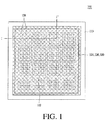
- FIG. 1 is a plan view illustrating a structure of a lighting apparatus using an organic light emitting diode according to the present disclosure.
- a lighting apparatus 100 is a surface emission lighting apparatus and a first electrode 124 and a second electrode 126 are disposed over the entire surface of the first substrate 110 and an organic light emitting layer 130 is disposed between the first electrode 124 and the second electrode 126 to form an organic light emitting diode.
- a signal is applied to the first electrode 124 and the second electrode 126 of the organic light emitting diode to cause the organic light emitting layer 130 to emit light so that light is output from the entire substrate 110.
- An auxiliary electrode 122 is disposed on the first substrate 110 in a matrix.
- the auxiliary electrode 122 is made of a metal having a good conductivity to apply uniform voltage to the first electrode 124 disposed in the entire area of the first substrate 110 so that a large size lighting apparatus 100 may emit light with uniform luminance.
- At least one conductive pattern 128 is disposed above or below the first electrode 124. In this case, the at least one conductive pattern 128 is disposed in a closed curve of the auxiliary electrode 122.
- the organic light emitting layer 130 is made of an organic light emitting material which outputs white light.
- the organic light emitting layer 130 may be configured by a blue organic light emitting layer, a red organic light emitting layer, and a green organic light emitting layer or may be configured by a tandem structure including a blue light emitting layer and a yellow-green light emitting layer.
- the organic light emitting layer 130 of the present disclosure is not limited to the above-described structure and various structures may be applied therefor.
- the organic light emitting layer 130 of the present disclosure may further include an electron injection layer and a hole injection layer which inject electrons and holes to the organic light emitting layer, respectively and an electron transport layer and a hole transport layer which transport the injected electrons and holes to the organic light emitting layer, respectively, and a charge generating layer which generates charges such as electrons and holes.
- first pad and a second pad which are connected to the first electrode 124 and the second electrode 126, respectively, to be applied with a voltage from the outside are disposed on the first substrate 110.
- the first pad and the second pad may be formed at one edge of the first substrate 110 or may be formed at both edges, respectively.
- a plurality of first pads and second pads may be provided to be disposed at four edges of the first substrate 110.
- FIG. 2 is a cross-sectional view taken along the line I-I' of FIG. 1 and the lighting apparatus 100 according to the present disclosure will be described in more detail with reference to FIG. 2 .
- the at least one conductive pattern 128 and the first electrode 124 are disposed on the first substrate 110 which is formed of a bendable transparent material having flexibility such as plastic or a rigid transparent material such as glass.
- the above-described conductive pattern 128 is formed of a transparent metal oxide such as indium tin oxide (ITO) or indium zinc oxide (IZO).
- the first electrode 124 uses a transparent conductive material having a high resistance and the reason therefor will be described in detail below.
- the first electrode 124 is disposed over an area excluding an outer edge area of the first substrate 110, but at least one conductive pattern 128 is disposed to have a predetermined size.
- the conductive patterns 128 and the first electrode 124 are in direct contact with each other to be electrically connected.
- the conductive pattern 128 is disposed below the first electrode 124 to be electrically connected, the conductive pattern 128 may be disposed above the first electrode 124 to be connected to the first electrode.
- first pad and the second pad may be disposed at the edge area of the first substrate 110.
- first pad and the second pad may be formed of the same material as the first electrode 124 by the same process.
- the auxiliary electrode 122 is disposed on the first substrate 110 to be electrically connected to the first electrode 124.
- the first electrode 124 is formed of a transparent conductive material to have an advantage in that the emitted light may pass through the first electrode, but also have a disadvantage in that an electric resistance is very high as compared with metal. Therefore, when a large size lighting apparatus 100 is manufactured, the distribution of the current applied to a large lighting area is not uniform due to a high resistance of the transparent conductive material and the large size lighting apparatus 100 may not emit light with uniform luminance due to the ununiform current distribution.
- the auxiliary electrode 122 is disposed over the entire first substrate 110 to have a matrix type with a small thickness, a mesh type, a hexagonal shape, an octagonal shape, or a circular shape to allow a uniform voltage to be applied to the first electrode 124 of the entire first substrate 110. Therefore, the light with a uniform luminance may be emitted from the large size lighting apparatus 100.
- the auxiliary electrode 122 is disposed below the first electrode 124 in the drawing, the auxiliary electrode 122 may be disposed above the first electrode 124.
- the auxiliary electrode 122 is made of a metal having a good conductivity, such as Al, Au, Cu, Ti, W, Mo, or an alloy thereof.
- the auxiliary electrode 122 has a single layer structure, the auxiliary electrode 122 may be configured by a plurality of layers including two or more layers.
- the auxiliary electrode 122 is disposed in a matrix to divide the first substrate 110 into a plurality of pixel units. That is, the auxiliary electrode 122 has a very low resistance as compared with the first electrode 124 so that substantially, the voltage of the first electrode 124 is not directly applied to the first electrode 124 through the first pad, but is applied through the auxiliary electrode 122. Therefore, even though the first electrode 124 is formed over the entire first substrate 110, the first electrode 124 is divided into a plurality of pixels by the auxiliary electrode 122.
- the auxiliary electrode 122 is formed to have a width of approximately 40 to 60 ⁇ m, but the auxiliary electrode 122 may be determined by various factors such as a type of metal to be used, an area of the lighting apparatus 100, or a size of the pixel.
- the at least one conductive pattern 128 is disposed in each pixel to be spaced apart from each other. Specifically, the at least one conductive pattern 128 is disposed in the emission region of each pixel.
- the conductive pattern 128 is configured to have a square shape, the shape of the conductive pattern 128 is not limited to a specific shape such as a square shape, but may be formed of various shapes such as polygons including a circle, an oval, a triangle, or a pentagon.
- a predetermined number of conductive patterns 128 is regularly disposed in a matrix, the conductive patterns 128 are not disposed to have a specific number or a specific shape, but may be disposed to have various numbers and various shapes.
- the at least one conductive pattern 128 may be formed of the same material as the auxiliary electrode 122.
- a protective layer 112 is laminated above the first electrode 124 of the first substrate 110.
- the protective layer 112 is configured to cover the auxiliary electrode 122 and the first electrode 124 above the auxiliary electrode 122. Since the auxiliary electrode 122 is made of opaque metal, the light is not output to an area where the auxiliary electrode 122 is formed. Therefore, the protective layer 112 is provided only above the auxiliary electrode 122 and is not disposed in an actual emission area (that is, a pixel) so that the light is emitted only from the emission area of the pixel to be output.
- the protective layer 112 is formed to enclose the auxiliary electrode 122 to reduce a step caused by the auxiliary electrode 122. Therefore, various layers formed thereafter are stably formed without being disconnected.
- the cross section of the auxiliary electrode 122 may be tapered or have a tapered shape, and the cross section of the protective layer 112 may have the same taper shape.
- the protective layer 112 is made of an inorganic layer such as SiOx or SiNx.
- the protective layer 112 may be configured by an organic layer such as photoacryl or also configured by a plurality of layers of inorganic layers and organic layers.
- the organic light emitting layer 130 and the second electrode 126 are disposed above the first electrode 124 and the protective layer 112.
- the organic light emitting layer 130 is a white light emitting layer and may be configured by a red light emitting layer, a blue light emitting layer, and a green light emitting layer or may be configured by a tandem structure including a blue light emitting layer and a yellow-green light emitting layer. Further, the organic light emitting layer 130 may further include an electron injection layer and a hole injection layer which inject electrons and holes to the organic light emitting layer, respectively and an electron transport layer and a hole transport layer which transport the injected electrons and holes to the organic light emitting layer, respectively, and a charge generating layer which generates charges such as electrons and holes.
- a material which receives holes and electrons from the hole transport layer and the electron transport layer to couple the holes and electrons to emit light in a visible light region and has a good quantum efficiency for fluorescence or phosphorescence is desirable for the organic light emitting layer 130.
- organic material may include 8-hydroxy-quinoline aluminum complex (Alq3), a carbazole based compound, a dimerized styryl compound, BAlq, a 10-hydroxybenzoquinoline-metal compound, benzoxazole, benzothiazole, and benzimidazole-based compounds, and poly (p-phenylenevinylene) (PPV), but are not limited thereto.
- the second electrode 126 may be configured by a metal such as Ca, Ba, Mg, Al, Ag, or an alloy thereof. Even though not illustrated in the drawing, a second pad which is connected to the second electrode 126 to apply a voltage to the second electrode 126 is provided above an outer edge of the first substrate 110.
- the first electrode 124, the organic light emitting layer 130, and the second electrode 126 configure the organic light emitting diode.
- the first electrode 124 serves as an anode of the organic light emitting diode and the second electrode 126 serves as a cathode of the organic light emitting diode.
- the voltage is applied to the first electrode 124 and the second electrode 126, the electrons from the second electrode 126 are injected into the organic light emitting layer 130 and the holes from the first electrode 124 are injected into the organic light emitting layer 130. Thereafter, excitons are generated in the organic light emitting layer 130.
- the protective layer 112 is disposed above the auxiliary electrode 122 so that the organic light emitting layer 130 above the auxiliary electrode 122 is not in direct contact with the first electrode 124. Therefore, the organic light emitting diode is not formed above the auxiliary electrode 122. In other words, the organic light emitting diode in the lighting apparatus 100 is formed only in a pixel between auxiliary electrodes 122 formed in a matrix.
- An adhesive agent 118 is applied on the first substrate 110 equipped with the organic light emitting diode and a second substrate 170 is disposed thereon so that the second substrate 170 is attached by the adhesive agent 118. By doing this, the lighting apparatus 100 is sealed.
- the adhesive agent 118 may use a photo-curing adhesive or a thermosetting adhesive.
- the second substrate 170 may be configured by various materials. As illustrated in the drawing, the adhesive agent 118 is also provided on the side of the organic light emitting diode to completely seal the organic light emitting diode.
- the second substrate 170 is provided to suppress moisture or air from permeating from the outside, so that any material which performs the above-mentioned function may be used.
- the second substrate 170 may be configured by a polymer such as polyethyleneterephtalate (PET) or a thin metal foil such as aluminum.
- a protective layer configured by an organic layer and/or inorganic layer and an encapsulating agent configured by an epoxy compound, an acrylate compound, or an acrylic compound may be provided on the second electrode 126 and on the side of the organic light emitting diode.
- the first electrode 124 is made of a transparent conductive material having a high resistance so that it is possible to suppress the failure caused by the short-circuit generated when the first electrode 124 and the second electrode 126 are in electrical contact with each other, which will be described in more detail below.
- FIG. 3A is a view schematically illustrating a circuit of an organic light emitting diode provided in a lighting apparatus.
- voltages V1 and V2 are applied to the first electrode 124 and the second electrode 126, respectively and resistors R E1 , R E2 , ..., R En of the organic light emitting layer 130, resistors R 11 , R 12 , ..., R 1n of the first electrode 124, and resistors R 21 , R 22 , ..., R 2n of the second electrode 126 are connected in series between the first electrode 124 and the second electrode 126.
- An organic light emitting diode provided in the lighting apparatus includes a plurality of pixels P 1 , P 2 , ..., P n and the pixels are connected in parallel with other pixels.
- the plurality of pixels is connected in parallel to apply voltages V1 and V2 to the first electrode 124 and the second electrode 126, respectively. Therefore, currents I 1 , I 2 , ..., I n are applied to organic light emitting layers LED1, LED2, ..., LEDn of the pixels P 1 , P 2 , ..., P n so that the organic light emitting layers LED1, LED2, ..., LEDn emit light.
- a voltage V1 having a set magnitude may be applied to the first electrode 124 and the second electrode 126 may be grounded.
- the organic light emitting layer 130 of the organic light emitting diode is formed to have a thin thickness of several hundred ⁇ . Therefore, when foreign materials penetrate into the organic light emitting layer 130 due to a process failure, pinholes or cracks are generated in the organic light emitting layer 130. Therefore, the first electrode 124 and the second electrode 126 are in contact with each other through the organic light emitting layer 130, which may cause a short. Further, in the case of the lighting apparatus, various metal layers and insulating layers are formed below the organic light emitting layer 130. In this case, the organic light emitting layer 130 is cracked due to a step of the metal layer and the insulating layer so that the first electrode 124 and the second electrode 126 may be in contact with each other. Further, since the organic light emitting material is ununiformly applied due to a process failure or a process error during the laminating process of the organic light emitting layer 130, the first electrode 124 and the second electrode 126 may be electrically connected to each other.
- FIG. 3B is a view illustrating a circuit of an organic light emitting diode when an electric short is generated in the first electrode 124 and the second electrode 126.
- the resistance R E2 by the organic light emitting layer 130 is removed from the pixel so that only the resistances R 12 and R 22 by the conductive material of the first electrode 124 and the second electrode 126 remain.
- the first electrode 124 is formed of a transparent metallic oxide material having a relatively good conductivity, such as indium tin oxide (ITO) or indium zinc oxide (IZO), resistances R 11 , R 12 , ..., R 1n of the first electrode 124 are approximately 20 ⁇ . Further, the resistances R 21 , R 22 , ..., R 2n of the second electrode 126 formed of metal are approximately 0.1 ⁇ . In contrast, the resistances R E1 , R E2 , ..., R En of the organic light emitting layer 130 are approximately 1 M ⁇ .
- ITO indium tin oxide
- IZO indium zinc oxide
- the resistances R E1 , R E2 , ..., R En of the organic light emitting layer 130 are much higher than the resistances R 11 , R 12 , ..., R 1n of the first electrode 124 and the resistances R 21 , R 22 , ..., R 2n of the second electrode 126. Therefore, total resistances Rt1, Rt2, ..., Rtn of the pixels P 1 , P 2 , ..., P n are substantially equal to the resistances R E1 , R E2 , ..., R En of the organic light emitting layer 130 (Rt ⁇ R E ).
- the current Ie between the first electrode 124 and the second electrode 126 mostly flows through the short-circuited pixel P 2 and hardly flows through other pixels P 1 , ..., P n . Therefore, the luminance of the organic light emitting layer of the pixels P 1 , ..., P n is rapidly degraded or the organic light emitting layer does not emit light.
- the auxiliary electrode 122 having a good conductivity is provided in the lighting apparatus and the signal is substantially applied to the first electrode 124 of each of the pixels P 1 , P 2 , ..., P n through the auxiliary electrode 122.
- overcurrent Ie flows in the short-circuited pixel P2 so that a temperature of the short-circuited area is increased to degrade the organic light emitting layer 130 of the organic light emitting diode.
- the first electrode 124 is formed of a transparent conductive material having a relatively high resistance so that a separate short reduction resistor is provided in each of the pixels P 1 , P 2 , ..., P n of the organic light emitting diode.
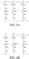
- FIGS. 4A and 4B are circuit diagrams of an organic light emitting diode including a separate short reduction resistor.
- the resistance R E2 by the organic light emitting layer 130 is removed so that only the resistances R 12 and R 22 by the conductive material of the first electrode 124 and the second electrode 126 and the short reduction resistance R SR2 remain.
- the first electrode 124 is formed of a transparent metallic oxide material having a relatively good conductivity, such as indium tin oxide (ITO) or indium zinc oxide (IZO), resistances R 11 , R 12 , ..., R 1n of the first electrode 124 are approximately 20 ⁇ . Further, the resistances R 21 , R 22 , ..., R 2n of the second electrode 126 formed of metal are approximately 0.1 ⁇ . In contrast, the resistances R E1 , R E2 , ..., R En of the organic light emitting layer 130 are approximately 1 M ⁇ .
- ITO indium tin oxide
- IZO indium zinc oxide
- the resistances R E1 , R E2 , ..., R En of the organic light emitting layer 130 are much higher than the resistances R 11 , R 12 , ..., R 1n of the first electrode 124 and the resistances R 21 , R 22 , ..., R 2n of the second electrode 126. Therefore, the total resistances Rt1, Rt2, ..., Rtn of each of the pixels P 1 , P 2 , ..., P n are substantially equal to the resistances R E1 , R E2 , ..., R En of the organic light emitting layer 130 (Rt ⁇ R E ).
- total resistances Rt1, Rt2, ..., Rtn of the pixels P 1 , P 2 , ..., P n are not substantially equal to the resistances R E1 , R E2 , ..., R En of the organic light emitting layer 130.
- the total resistances Rt1, Rt2, ..., Rtn of the pixels P 1 , P 2 , ..., P n are substantially equal to a sum of the resistances R E1 , R E2 , ..., R En of the organic light emitting layer 130 and the short reduction resistances R SR1 , R SR2 , ..., R SRn (Rt1, Rt2, ..., Rtn ⁇ R E1 , R E2 , ..., R En + R SR1 , R SR2 , ..., R SRn ).
- the short reduction resistance R SR2 is not so very lower than the resistance R E2 of the organic light emitting layer 130, but has a significant magnitude. Therefore, the current between the first electrode 124 and the second electrode 126 does not mostly flow through the short-circuited pixel P 2 , but a predetermined amount of current I' 2 flows through the pixel P 2 .
- magnitudes of the short reduction resistances R SR1 , R SR2 , ..., R SRn are appropriately set so that even though the first electrode 124 and the second electrode 126 of one pixel among the plurality of pixels P 1 , P 2 , ..., P n are in contact with each other, overcurrent does not flow through the short-circuited pixel but a set current flows. Therefore, the lowering of the luminance of the organic light emitting diode may be suppressed.
- the first electrode 124 may be made of a transparent conductive material and has a resistance of at least half of that of the organic light emitting layer 130, for example, the resistance of the first electrode 124 may be 2800 to 5500 ⁇ .
- the resistance of the first electrode 124 may be 2800 to 5500 ⁇ .
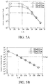
- FIG. 5A is a graph illustrating a relationship between a pixel current and a short reduction resistance which are applied to the pixels P 1 , P 2 , ..., P n when no short-circuit is generated in the pixels P 1 , P 2 , ..., P n of an organic light emitting diode
- FIG. 5B is a graph illustrating a relationship between a short current and a short reduction resistance which are applied to the short-circuited pixels P 1 , P 2 , ..., P n when a short-circuit is generated in the pixels P 1 , P 2 , ..., P n of an organic light emitting diode.
- FIGS. 5A is a graph illustrating a relationship between a pixel current and a short reduction resistance which are applied to the pixels P 1 , P 2 , ..., P n when no short-circuit is generated in the pixels P 1 , P 2 , ..., P n of an organic light emitting diode
- the organic light emitting diode when no short-circuit is generated in the pixels P 1 , P 2 , ..., P n of the organic light emitting diode, the organic light emitting diode is normally driven to emit light from the entire organic light emitting diode.
- the current required to normally drive the organic light emitting diode may vary depending on the size of the pixels P 1 , P 2 , ..., P n .
- the organic light emitting diode is normally driven to emit light.
- the short current is applied to the short-circuited pixel so that the organic light emitting diode is not normally driven.
- the short current flowing in the short-circuited pixel of the organic light emitting diode exceeds approximately 1.34 mA, a current which is applied to the other pixel is rapidly lowered due to the overcurrent of the short-circuited pixel so that the entire luminance of the organic light emitting diode is degraded.
- the short current applied to the short-circuited pixel of the organic light emitting diode is rapidly increased.
- the short reduction resistances R SR1 , R SR2 , ..., R SRn are lowered to 2800 ⁇ , the short current applied to the short-circuited pixel of the organic light emitting diode exceeds 1.34 mA. Therefore, the entire luminance of the organic light emitting diode is degraded.
- the short reduction resistances R SR1 , R SR2 , ..., R SRn are further lowered to 2800 ⁇ or lower, the short current is further increased so that the organic light emitting diode is unable to be driven. Therefore, when the magnitude of the short reduction resistances R SR1 , R SR2 , ..., R SRn of the short-circuited pixel is 2800 ⁇ or lower, the organic light emitting diode is unable to be driven due to the increased short current.
- the short reduction resistances R SR1 , R SR2 , ..., R SRn of the plurality of pixels P 1 , P 2 , ..., P n are 5500 ⁇ or higher, the luminance of the organic light emitting diode is significantly degraded. Further, when the short reduction resistances R SR1 , R SR2 , ..., R SRn of the plurality of pixels P 1 , P 2 , ..., P n are 2800 ⁇ or lower, the entire luminance of the organic light emitting diode is degraded.
- the short reduction resistances R SR1 , R SR2 , ..., R SRn of the plurality of pixels P 1 , P 2 , ..., P n are desirably set in the range of 2800 ⁇ ⁇ R SR ⁇ 5500 ⁇ .
- the short reduction resistances R SR1 , R SR2 , ..., R SRn may be configured to have various shapes.
- a resistive layer having a predetermined resistance for example, 2800 ⁇ to 5500 ⁇ is provided between the first electrode 124 and the organic light emitting layer 130 and/or between the second electrode 126 and the organic light emitting layer 130 to add short reduction resistances R SR1 , R SR2 , ..., R SRn to each of the pixels P 1 , P 2 , ..., P n of the organic light emitting diode.
- a resistive pattern having a set resistance is added to each pixel of the lighting apparatus 100 having a structure illustrated in FIG. 1 to add the short reduction resistances R SR1 , R SR2 , ..., R SRn to the pixels P 1 , P 2 , ..., P n .
- a separate resistive pattern is added after electrically separating the auxiliary electrode 122 and the first electrode 124 in each pixel of the lighting apparatus 100 having a structure illustrated in FIG. 1 to add the short reduction resistances R SR1 , R SR2 , ..., R SRn .
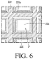
- FIG. 6 is a view illustrating an example of a structure of a lighting apparatus including a short reduction resistor by forming a separate pattern in a pixel.
- a first electrode 224 is formed to be spaced apart from the auxiliary electrode 222 with a predetermined distance and the auxiliary electrode 222 and the first electrode 224 are electrically connected to each other by a resistive pattern 224a having a relatively high resistance.
- the signal which is applied to the auxiliary electrode 222 is applied to the first electrode 224 via the resistive pattern 224a, so that short reduction resistances R SR1 , R SR2 , ..., R SRn having a desired magnitude may be formed by forming the resistance pattern 224a to be sufficiently long (that is, by making a path through which the signal flows sufficiently long).
- the resistive pattern 224a which is formed of the same material as the first electrode 224 is formed by forming the first electrode 224 over the entire lighting apparatus including an upper portion of the auxiliary electrode 222 and forming an open area 225 obtained by removing a part of the first electrode 224.
- the resistive pattern 224a may be formed by the same material as or a different material from the first electrode 224 through a different process from the first electrode 224.
- an area where the resistive pattern 224a is formed does not emit light so that an aperture ratio (a ratio of an emission area) of the lighting apparatus is lowered.
- the resistive pattern 224a needs to be formed to have a set width and a set length to form a set resistance, so that the resistive pattern 224a needs to be formed in the pixel to have a predetermined area regardless of the area of the pixels. Therefore, in the case of a high definition lighting apparatus in which the size of the pixel is small, the aperture ratio is lowered due to the resistive pattern 224a to be a set value or lower, so that the lighting apparatus may be defective. Therefore, when the short reduction resistances R SR1 , R SR2 , ..., R SRn are formed by the resistive pattern 224a, the aperture ratio of the pixel is lowered so that a high definition lighting apparatus cannot be manufactured.
- the first electrode 124 is formed using a conductive material having a high resistance without providing a separate resistive layer or resistive pattern, to form the short reduction resistances R SR1 , R SR2 , ..., R SRn in each pixel.
- a separate resistive layer or resistive pattern is not provided, so that problems in that a process is added, the aperture ratio is lowered, and the high definition lighting apparatus cannot be manufactured may be solved.
- the transparent conductive material having a high resistance used for the first electrode 124 of the present disclosure sets the resistance in the pixel to be approximately 2800 to 5500 ⁇ . Therefore, even though the first electrode and the second electrode are in contact with each other, a failure of the lighting apparatus 100 due to the short-circuit of the pixel may be suppressed.
- any transparent conductive material having a resistance in the above-mentioned range may be used, for example, a conductive polymer, a carbon based material, or a nanowire based material may be used.
- FIGS. 7A and 7B are views illustrating a circuit of an organic light emitting diode according to the present disclosure in which a first electrode 124 is formed of a conductive material having a high resistance.
- the resistors R E1 , R E2 , ..., R En of the organic light emitting layer 130, the resistors R' 11 (SR1), R' 12 (SR2), ..., R' 1n (SRn) of the first electrode 124, and the resistors R 21 , R 22 , ..., R 2n of the second electrode 126 are connected in series, in the plurality of pixels P 1 , P 2 , ..., P n which are connected in parallel.
- resistances R 21 , R 22 , ..., R 2n of the second electrode 126 formed of metal such as Ca, Ba, Mg, Al, or Ag or an alloy thereof are approximately 0.1 ⁇ and resistances R E1 , R E2 , ..., R En of the organic light emitting layer 130 are approximately 1 M ⁇ .
- the resistances R' 11 (SR1), R' 12 (SR2), ..., R' 1n (SRn) of the first electrode 124 which is formed of a high resistance conductive material such as a conductive polymer, a carbon based material, or a nanowire based material are approximately 2800 to 5500 ⁇ .
- a separate short reduction resistance is provided in the organic light emitting diode illustrated in FIG. 4A .
- a separate short reduction resistance is not formed and the first electrode 124 has a high resistance to serve as a short reduction resistor.
- the resistances R' 11 (SR1), R' 12 (SR2), ..., R' 1n (SRn) are approximately 2800 to 5500 ⁇ and the resistances R E1 , R E2 ,..., R En of the organic light emitting layer 130 are approximately 1 M ⁇ . Therefore, even though the resistance R E2 of the organic light emitting layer 130 of the second pixel P 2 is removed by the contact of the first electrode 124 and the second electrode 126, the resistance R' 12 (SR2) by the high resistance transparent conductive material of the first electrode 124 remains in the short-circuited second pixel P 2 . However, the magnitude of the resistance R' 12 (SR2) is not ignorable as compared with the magnitude of the total resistances of the other pixels P 1 , ..., P n .
- a total resistance Rt2 of the second pixel P 2 is substantially equal to the resistance R' 12 (SR2) of the first electrode 124 (Rt2 ⁇ R' 12 (SR2)).
- the resistance R' 12 (SR2) of the first electrode 124 is not so very lower than the resistance R E2 of the organic light emitting layer 130, but has a significant magnitude. Therefore, the current between the first electrode 124 and the second electrode 126 does not mostly flow through the short-circuited pixel P 2 , but a predetermined amount of current I' 2 flows through the pixel P 2 . In this case, even though an amount of current flowing through the second pixel P 2 and an amount of current flowing through other pixels P 1 , ..., P n are different due to the difference in a total resistance of the second pixel P 2 and other pixels P 1 , ..., P n , the current flows through the entire pixels P 1 , P 2 , ..., P n . Therefore, a phenomenon in that the luminance of the organic light emitting layer of the plurality of pixels P 1 , P 2 , ..., P n is rapidly degraded or the organic light emitting layer does not emit light may be suppressed.
- the short-circuit of the pixels P 1 , P 2 , ..., P n is suppressed without providing a separate resistive layer, so that the cost increased due to the addition of the process or the lowering of the yield may be suppressed.
- the short-circuit of the pixels P 1 , P 2 , ..., P n is suppressed without providing a separate resistive pattern so that the lowering of the aperture ratio of the lighting apparatus is suppressed. Specifically, it is more effectively used for a high definition lighting apparatus having a pixel area of 300 ⁇ 300 ⁇ m 2 .
- a at least one conductive pattern 128 having a set size below (or above) the first electrode 124 formed of a conductive material having a high resistance is disposed in the pixel.
- the conductive pattern 128 improves a conductivity in each pixel P 1 , P 2 , ..., P n to improve luminance of the organic light emitting diode.
- the first electrode 124 serving as an anode electrode is made of a transparent conductive material having a high resistance, so that even though the first electrode 124 and the second electrode 126 are in contact with each other, the short-circuit of the pixel may be suppressed without providing a short reduction resistor.
- the resistance is much higher than that of a transparent metal oxide which has been used in the related art, such as ITO or IZO. That is, a resistance of the transparent metal oxide which has been used in the related art, such as ITO or IZO is approximately 20 ⁇ , but the resistance of the high resistance conductive material which is used in the present disclosure is approximately 2800 to 5500 ⁇ . Therefore, the resistance of the high resistance conductive material of the present disclosure is much higher than the resistance of the transparent metal oxide. Therefore, when the first electrode 124 is formed of a high resistance transparent conductive material, the short-circuit of the pixel may be suppressed. However, the luminance of the organic light emitting diode is degraded due to a relatively high resistance.
- the conductive pattern 128 suppresses the lowering of the luminance by the first electrode 124 configured by the high resistance conductive material. That is, a at least one conductive pattern 128 is formed in the pixels P 1 , P 2 , ..., P n to be an island shape while being electrically connected to the first electrode 124 to improve conductivity of the first electrode 124 in the pixels P 1 , P 2 , ..., P n for every area.
- the short-circuit of the pixels P 1 , P 2 , ..., P n of the organic light emitting diode is suppressed by the first electrode 124 which is formed of a high resistance conductive material and the conductive pattern 128 and the lowering of the luminance of the organic light emitting diode is also suppressed.
- the at least one conductive pattern 128 is provided in each pixel P 1 , P 2 , ..., P n so that the conductive pattern 128 and the second electrode 126 are in contact with each other. Therefore, the pixel may be short-circuited.
- the short-circuit due to the contact of the conductive pattern 128 and the second electrode 126 is restricted to the predetermined area of the pixel, so that defectiveness of the entire pixels may be suppressed.
- FIGS. 8A and 8B are views illustrating a state in which the first electrode 124 and the second electrode 126 are in electrical contact with each other due to pinholes or cracks in a light emitting diode according to the present disclosure in which FIG. 8A is a plan view and FIG. 8B is a cross-sectional view.
- At least one conducive pattern 128 is disposed in the pixel P which is divided by the auxiliary electrode 122 and the conductive pattern 128 is disposed below (or above) the first electrode 124 to be in entire contact with the first electrode 124.
- the first electrode 124 disposed in the pixel P is formed of a transparent conductive material having a high resistance, but a conductive pattern 128 having a relatively low resistance is formed in the pixel P. Therefore in an area where the first electrode 124 and the conductive pattern 128 are in contact with each other, the resistance of the first electrode 124 is removed by the conductive pattern 128, and only the resistance by the conductive pattern 128 remains.
- a total resistance Rt of the first electrode 124 in the pixel P is reduced by the conductive pattern 128.
- a contact area C where the first electrode 124 and the second electrode 126 are in electrical contact with each other is generated. Further, since the first electrode 124 is in contact with the conductive pattern 128, the conductive pattern 128 and the second electrode 126 are electrically connected through the contact area C.
- the failure due to the short-circuit makes only the contact area C in the pixel P defective and the other area does not become defective. Therefore, the other area than the contact area C in the pixel P emits light so that defectiveness of the pixel P may be suppressed.
- the first electrode 124 uses a transparent conductive material having a high resistivity so that the first electrode serves as the short reduction resistor without providing a separate resistive layer or resistive pattern. Therefore, even though the first electrode and the second electrode are in contact with each other, the failure due to the short-circuit of the organic light emitting diode may be suppressed.
- the aperture ratio of each pixel of the lighting apparatus of the disclosure may be at least 80%.
- an aperture ratio is approximately 84.1%.
- the aperture ratio is approximately 93.3%. Therefore, the aperture ratio of the lighting apparatus according to the present disclosure is improved by approximately 9% as compared with the lighting apparatus having a structure including a resistive pattern.
- an aperture ratio is approximately 74.1%.
- the aperture ratio is approximately 89%. Therefore, the aperture ratio of the lighting apparatus according to the present disclosure is improved by approximately 15% as compared with the lighting apparatus having a structure including a resistive pattern.
- the aperture ratio of the present disclosure is improved as compared with that of the structure including a resistive pattern and the degree of improvement of the aperture ratio is more obvious in the high definition lighting apparatus having a smaller pixel area.
- an aperture ratio is approximately 62.1%.
- the aperture ratio is approximately 83.7%. Therefore, the present disclosure may be applied to the lighting apparatus having a pixel size of 200 ⁇ 200 ⁇ m 2 , but the structure including a resistive pattern may not be used for the lighting apparatus of 200 ⁇ 200 ⁇ m 2 due to the lowering of the aperture ratio.
- At least one conductive pattern 128 having a low resistance and a good conductivity is disposed in each pixel to suppress the degradation of the luminance by the first electrode 124 having a high resistance.
- the lighting apparatus 100 of the present disclosure may suppress the lowering of luminance and also suppress the failure due to the short-circuit even when the first electrode 124 and the second electrode 126 are in contact with each other due to a process error.
- FIGS. 9A to 9D and FIGS. 10A to 10D are views illustrating a manufacturing method of a lighting apparatus 100 in which FIGS, 9A to 9D are plan views and FIGS. 10A to 10D are cross-sectional views.
- auxiliary electrode 122 formed of a single layer or a plurality of layers by laminating and etching metal such as Al, Au, Cu, Ti, W, Mo, or an alloy thereof on a transparent first substrate 110 formed of a flexible material such as plastic or a rigid material such as glass
- at least one conductive pattern 128 is formed on a plurality of pixels divided by the auxiliary electrode 122 by laminating and etching a transparent metal oxide such as ITO or IZO on the first substrate 110.
- the auxiliary electrode 122 is disposed in a matrix in a horizontal direction and a vertical direction to have a strip shape set over the entire first substrate 110, but the auxiliary electrode 122 may be formed to have a mesh type, a hexagonal shape, an octagonal shape, or a circular shape. Further, at least one conductive pattern 128 may be disposed to have various shapes such as a polygon, a triangle, or a circle.
- the auxiliary electrode 122 may be formed to have a width of approximately 45 to 55 ⁇ m. However, the auxiliary electrode 122 is not limited to have a specific width, but the auxiliary electrode 122 may be formed to have various widths depending on an area of the lighting apparatus, a size of the pixel, and a material of the auxiliary electrode 122.
- the conductive pattern 128 may be formed after forming the auxiliary electrode 122, but the auxiliary electrode 122 may be formed after forming the conductive pattern 128 in the plurality of pixels.
- a conductive polymer such as approximately 1 to 10 wt% of poly (3,4-ethylenedioxythiophene): polystyrenesulfonic acid (PEDOT:PSS) in a solvent such as approximately 80 to 90 wt% of water or alcohol
- a silicone binder such as approximately 10 to 20 wt% of TEOS (Tetraethlyorthosilicate), SSQ (Silsesquioxane), or polysiloxane or an acrylic binder is mixed, and an additive such as a leveling agent and a surface agent within 1 wt% is added to form a transparent conductive material having a high resistivity (or a transparent conductive layer with high resistance).
- a silicone binder such as approximately 10 to 20 wt% of TEOS (Tetraethlyorthosilicate), SSQ (Silsesquioxane), or polysiloxane or an acrylic binder is mixed, and an additive such as a leveling agent and a surface agent within 1 wt% is added to form a transparent conductive material having a high resistivity (or a transparent conductive layer with high resistance).
- a silicone binder such as approximately 10 to 20 wt% of TEOS (Tetraethlyorthosilicate), SSQ (Silsesquioxane), or polysiloxane or an acrylic binder is mixed, and an additive such as a leveling agent and a surface agent within 1 wt% is added to form a transparent conductive material having a high resistivity (or a transparent conductive layer with high resistance).
- the high resistivity transparent conductive material as described above is laminated and etched over the entire first substrate 110 including the auxiliary electrode 122 and the upper surface of the conductive pattern 128 to form the first electrode 124.
- the first electrode 124 may be formed to have a different thickness depending on the type of conductive material. For example, when the conductive polymer is used as a conductive material, the first electrode 124 is formed to have a thickness of approximately 150 to 200 nm and when the carbon based material is used as the conductive material, the first electrode 124 may be formed to have approximately 50 to 100 nm.
- the auxiliary electrode 122 and the conductive pattern 128 may be formed on the first electrode 124.
- the protective layer 112 may be formed on the first electrode 124 above the auxiliary electrode 122 by laminating and etching an inorganic insulating material or an organic insulating material on the first electrode 124.
- the protective layer 112 may be configured by a single layer of an inorganic insulating layer or an organic insulating layer or may be configured by a plurality of layers of inorganic insulating layers and organic insulating layers.
- the organic light emitting layer 130 is formed by depositing an organic light emitting material above the first substrate 110.
- the organic light emitting layer 130 may be formed by depositing the organic light emitting material after disposing a mask on a mother substrate on which a plurality of lighting apparatuses is formed.
- the second electrode 126 is formed by depositing and etching a metal such as Ca, Ba, Mg, Al, or Ag above the organic light emitting layer 130.
- an adhesive agent 118 formed of a photo-curing adhesive material or a thermosetting adhesive material is applied on the first substrate 110, the second substrate 170 is positioned thereon, and then the adhesive agent 118 is hardened to attach the second substrate 170. Thereafter, the bonded first substrate 110 and second substrate 170 are cut to separate completed lighting apparatuses 100 and complete individual lighting apparatuses 100.
- a polymer film such as PET, a thin metal foil, or glass may be used for the second substrate 170.
- a lighting apparatus includes: a first substrate including a plurality of pixels; and an organic light emitting diode disposed in each pixel of the first substrate and comprises of a first electrode, an organic light emitting layer, and a second electrode, in which the first electrode is made of a transparent conductive material, the first electrode having a resistance of at least half of that of the organic light emitting layer in each pixel.
- the resistance of the first electrode may be 2800 to 5500 ⁇ .
- the first electrode may have a thickness of 50 to 200 nm.
- the lighting apparatus may further include: an auxiliary electrode disposed on the first substrate connected to the first electrode.
- the auxiliary electrode is arranged in a matrix type, a mesh type, an octagonal shape, a hexagonal shape, or a circular shape.
- the auxiliary electrode may have a width of 45 to 55 ⁇ m.
- the first electrode may be configured by at least one material selected from a group consisting of a conductive polymer, a carbon based material, and a nanowire based material.
- the lighting apparatus may further include at least one conductive pattern disposed in each of the plurality of pixels and electrically connected to the first electrode.
- the at least one conductive pattern may be disposed in an emission region of each pixel.
- the at least one conductive pattern may be formed of the same material as the auxiliary electrode.
- the lighting apparatus may further comprise a protective layer disposed on the axuliary electrode, wherein a cross section of the auxiliary electrode has a shape of taper or is tapered.
- a cross section of the protective layer may have the same taper shape as the auxiliary electrode.
- the at least one conductive pattern may be disposed in each pixel to have an island shape.
- the at least one conductive pattern may contact the first electrode.
- Each of the at least one conductive pattern may be configured by a polygonal shape, a circular shape, or an oval shape.
- the at least one conductive pattern may reduce a resistance of the first electrode in the pixel.
- a resistance of the first electrode in the pixel may be reduced as an area ratio of the at least one conductive pattern with respect to a pixel area is increased so that a luminance of the pixel is increased.
- the lighting apparatus may further include: a second substrate which is attached to the first substrate by an adhesive agent.
- An aperture ratio of each pixel may be at least 80%.
- a light emitting device comprising: a first substrate; an auxiliary electrode on the first substrate, the auxiliary electrode being disposed in a matrix to divide the first substrate into a plurality of pixels; a first electrode on the first substrate, the first electrode being electrically connected to the auxiliary electrode; an organic light emitting layer on the first electrode; and a second electrode on the organic light emitting layer, wherein the first electrode is made of a transparent conductive material whose resistance is at least half of that of the organic light emitting layer.
- a resistance of the fist electrode may be 2800 to 5500 ⁇ .
- the light emitting device may further comprise at least one conductive pattern disposed in each of the plurality of pixels and electrically connected to the first electrode.
Landscapes
- Physics & Mathematics (AREA)
- Optics & Photonics (AREA)
- Engineering & Computer Science (AREA)
- Manufacturing & Machinery (AREA)
- Electroluminescent Light Sources (AREA)
Abstract
Description
- The present disclosure relates to a lighting apparatus in which a failure due to a short-circuit is suppressed.
- Currently, fluorescent lamps or incandescent lamps are mainly used as lighting apparatuses. Among them, the incandescent lamps have a good color rendering index (CRI), but have a very low energy efficiency. Further, the fluorescent lamps have a good efficiency, but have a low color rendering index and contain mercury, which may cause an environmental problem.
- In order to solve the problems of the lighting apparatus of the related art, recently, a light emitting diode (LED) is suggested as a lighting apparatus . The light emitting diode is made of an inorganic light emitting material. A luminous efficiency is the highest in the blue wavelength range and the luminous efficiency is degraded toward a red wavelength range and a green wavelength range which has the highest visibility. Therefore, there is a problem in that when a red light emitting diode, a green light emitting diode, and a blue light emitting diode are combined to emit white light, the luminous efficiency is degraded. Further, there is another problem in that when the red light emitting diode, the green light emitting diode, and the blue light emitting diode are used, since widths of emission peaks are narrow, the color rendering property is also deteriorated.
- In order to solve the above-described problems, there has been proposed a lighting apparatus which outputs white light by combining a blue light emitting diode and a yellow fluorescent material to output white light, instead of a combination of the red light emitting diode, the green light emitting diode, and the blue light emitting diode. The reason why the light emitting diode configured as described above is proposed is that it is more effective to use only a blue light emitting diode having a high efficiency and a fluorescent material which receives blue light to emit yellow light for the remaining colors than to use a green light emitting diode having a low luminous efficiency.
- However, in the case of the lighting apparatus which combines the blue light emitting diode and a yellow fluorescent material to output white light, since the fluorescent material which emits yellow light has a low luminous efficiency, there is a limitation in improvement of the luminous efficiency of the lighting apparatus.
- In order to solve the problem in that the luminous efficiency is degraded, a lighting apparatus using an organic light emitting diode formed of an organic light emitting material has been proposed. Normally, the organic light emitting diode has relatively excellent luminous efficiencies of red and green light as compared with an inorganic light emitting diode. Further, widths of emission peaks of blue, red, and green light of the organic light emitting diode are relatively broader than that of the inorganic light emitting diode so that a color rendering property is improved. Therefore, there is an advantage in that light of the light emitting device is more similar to the sunlight.
- The organic light emitting diode comprises of an anode, a cathode, and an organic light emitting layer therebetween. However, in the organic light emitting diode used for the lighting apparatus, a distance between the anode and the cathode is small so that the anode and the cathode are brought in direct contact with each other due to pinholes or cracks due to permeation of foreign materials, a step of an internal structure of the organic light emitting diode, and roughness of laminated layers so that a short-circuit is caused between the anode and the cathode. Further, due to a process failure or a process error when the organic light emitting layer is formed, the organic light emitting layer is formed to be thinner than a set thickness so that there may be a problem in that the anode and the cathode are electrically short-circuited.
- When the anode and the cathode are electrically short-circuited, the short-circuit area forms a low resistance path through which a current flows so that the current flows only in the short-circuit area, but current which flows through the other area of the organic light emitting diode is considerably reduced or in extreme cases, the current does not flow. Therefore, the emission output of the organic light emitting diode is reduced or the organic light emitting diode does not emit light.
- When such an organic light emitting diode is applied to the lighting apparatus, light having luminance which is lower than a set luminance is emitted due to the short-circuit of the anode and the cathode so that a quality of the lighting apparatus is degraded or even the lighting apparatus does not operate. Further, when the organic light emitting diode is applied to the display device, pixels corresponding to the short-circuited area become defective pixels so that the quality of the display device is degraded.
- Generally, since organic light emitting diodes are manufactured in a clean room, the short-circuit of the anode and the cathode caused by foreign materials such as dusts permeating during a manufacturing process is avoided. Actually, even in the clean room, the permeation of the foreign materials cannot be perfectly avoided and the short-circuit due to a structural problem such as a step of an internal structure of the organic light emitting diode and the roughness of the laminated layers cannot be avoided. Therefore, the failure due to the short-circuit cannot be perfectly avoided.
- An object to be achieved by the present disclosure is to provide a lighting apparatus in which a first electrode of an organic light emitting diode is formed by a transparent conductive material having a high resistance which is equal to or higher than a set value to suppress the short-circuit due to contact of the first electrode and the second electrode.
- Another object to be achieved by the present disclosure is to provide a lighting apparatus in which at least one conductive pattern having a low resistance which is in contact with the first electrode in a plurality of pixels is formed to suppress degradation of luminance by the first electrode having a high resistance.
- There is provided, a lighting apparatus includes: a first substrate including a plurality of pixels; and an organic light emitting diode disposed in each of the plurality of pixels of the first substrate and comprising a first electrode, an organic light emitting layer, and a second electrode, in which the first electrode is made of a transparent conductive material and has a resistance of at least half of that of the organic light emitting layer in each pixel. Therefore, even though the first electrode and the second electrode are in contact with each other to remove a resistance by the organic light emitting layer in the pixel, an overcurrent is suppressed from being applied to the pixel due to the resistance of the first electrode.
- There is provided a light emitting device, comprising: a first substrate; an auxiliary electrode on the first substrate, the auxiliary electrode being disposed in a matrix to divide the first substrate into a plurality of pixels; a first electrode on the first substrate, the first electrode being electrically connected to the auxiliary electrode; an organic light emitting layer on the first electrode; and a second electrode on the organic light emitting layer, wherein the first electrode is made of a transparent conductive material whose resistance is at least half of that of the organic light emitting layer.
- According to the present disclosure, a first electrode which forms the organic light emitting diode is formed of a transparent conductive material having a high resistivity (the first electrode has a high resistance) so that even though the first electrode and the second electrode of the organic light emitting diode are in contact with each other, the short-circuit of the organic light emitting diode is suppressed. Therefore, degradation of the luminance of the lighting apparatus or a driving failure of the lighting apparatus due to the overcurrent which is applied through a pixel where the contact is generated may be suppressed.
- Specifically, according to the present disclosure, the short-circuit due to the contact of the first electrode and the second electrode is suppressed without forming a separate resistive layer or resistive pattern so that the complexity of the manufacturing process and the lowering of the aperture ratio may be suppressed.
- Further, according to the present disclosure, at least one transparent conductive pattern having a low resistance which is electrically connected to the first electrode is formed in each of a plurality of pixels so that a conductivity of the first electrode in the pixel is locally improved so that the degradation of the luminance of the lighting apparatus due to the first electrode having a high resistance may be suppressed.
- The above and other aspects, features and other advantages of the present disclosure will be more clearly understood from the following detailed description taken in conjunction with the accompanying drawings, in which:
-
FIG. 1 is a plan view illustrating a structure of a lighting apparatus according to the present disclosure; -
FIG. 2 is a cross-sectional view taken along the line I-I' ofFIG. 1 ; -
FIGS. 3A and 3B are views schematically illustrating a circuit of an organic light emitting diode provided in the lighting apparatus; -
FIGS. 4A and 4B are circuit diagrams of an organic light emitting diode including a separate short reduction resistor; -
FIG. 5A is a graph illustrating a relationship between a pixel current and a short reduction resistance which are applied to a pixel when no short-circuit is generated in the pixel of an organic light emitting diode; -
FIG. 5B is a graph illustrating a relationship between a short current and a short reduction resistance which are applied to a short-circuited pixel when a short-circuit is generated in the pixel of an organic light emitting diode; -
FIG. 6 is a view illustrating an example of a structure of a lighting apparatus including a short reduction resistor by forming a separate pattern in a pixel; -
FIGS. 7A and 7B are views illustrating a circuit of an organic light emitting diode according to the present disclosure in which a first electrode is formed of a conductive material having a high resistance; -
FIGS. 8A and 8B are views illustrating that a first electrode and a second electrode are in contact with each other in a predetermined area in a pixel due to pinholes and the like; -
FIGS. 9A to 9D are plan views illustrating a manufacturing method of a lighting apparatus according to the present disclosure; and -
FIGS. 10A to 10D are cross-sectional views illustrating a manufacturing method of a lighting apparatus according to the present disclosure. - Hereinafter, the present disclosure will be described in detail with reference to the accompanying drawings.
- In the present disclosure, provided is a lighting apparatus including an organic light emitting diode formed of an organic material, rather than a lighting apparatus including an inorganic light emitting diode formed of an inorganic material.
- The organic light emitting diode formed of an organic light emitting material has relatively excellent luminous efficiencies of red and green light as compared with an inorganic light emitting diode. Further, widths of emission peaks of blue, red, and green light of the organic light emitting diode are relatively broader than that of the inorganic light emitting diode so that a color rendering property is improved. Therefore, there is an advantage in that light of the light emitting device is more similar to the sunlight.
- Specifically, the present disclosure provides a light emitting device including an organic light emitting diode which may suppress the degradation of a luminous efficiency of the light emitting device or non-emission of the lighting apparatus when some of pixels of the organic light emitting diode are short-circuited.
-
FIG. 1 is a plan view illustrating a structure of a lighting apparatus using an organic light emitting diode according to the present disclosure. - As illustrated in
FIG. 1 , alighting apparatus 100 according to the present disclosure is a surface emission lighting apparatus and afirst electrode 124 and asecond electrode 126 are disposed over the entire surface of thefirst substrate 110 and an organiclight emitting layer 130 is disposed between thefirst electrode 124 and thesecond electrode 126 to form an organic light emitting diode. In thelighting apparatus 100 having the structure as described above, a signal is applied to thefirst electrode 124 and thesecond electrode 126 of the organic light emitting diode to cause the organiclight emitting layer 130 to emit light so that light is output from theentire substrate 110. - An
auxiliary electrode 122 is disposed on thefirst substrate 110 in a matrix. Theauxiliary electrode 122 is made of a metal having a good conductivity to apply uniform voltage to thefirst electrode 124 disposed in the entire area of thefirst substrate 110 so that a largesize lighting apparatus 100 may emit light with uniform luminance. - Further, at least one
conductive pattern 128 is disposed above or below thefirst electrode 124. In this case, the at least oneconductive pattern 128 is disposed in a closed curve of theauxiliary electrode 122. - The organic
light emitting layer 130 is made of an organic light emitting material which outputs white light. For example, the organiclight emitting layer 130 may be configured by a blue organic light emitting layer, a red organic light emitting layer, and a green organic light emitting layer or may be configured by a tandem structure including a blue light emitting layer and a yellow-green light emitting layer. However, the organiclight emitting layer 130 of the present disclosure is not limited to the above-described structure and various structures may be applied therefor. - Further, the organic
light emitting layer 130 of the present disclosure may further include an electron injection layer and a hole injection layer which inject electrons and holes to the organic light emitting layer, respectively and an electron transport layer and a hole transport layer which transport the injected electrons and holes to the organic light emitting layer, respectively, and a charge generating layer which generates charges such as electrons and holes. - Even though not illustrated in the drawing, a first pad and a second pad which are connected to the
first electrode 124 and thesecond electrode 126, respectively, to be applied with a voltage from the outside are disposed on thefirst substrate 110. In this case, the first pad and the second pad may be formed at one edge of thefirst substrate 110 or may be formed at both edges, respectively. Further, a plurality of first pads and second pads may be provided to be disposed at four edges of thefirst substrate 110. -
FIG. 2 is a cross-sectional view taken along the line I-I' ofFIG. 1 and thelighting apparatus 100 according to the present disclosure will be described in more detail with reference toFIG. 2 . - As illustrated in
FIG. 2 , the at least oneconductive pattern 128 and thefirst electrode 124 are disposed on thefirst substrate 110 which is formed of a bendable transparent material having flexibility such as plastic or a rigid transparent material such as glass. The above-describedconductive pattern 128 is formed of a transparent metal oxide such as indium tin oxide (ITO) or indium zinc oxide (IZO). Further, thefirst electrode 124 uses a transparent conductive material having a high resistance and the reason therefor will be described in detail below. - The
first electrode 124 is disposed over an area excluding an outer edge area of thefirst substrate 110, but at least oneconductive pattern 128 is disposed to have a predetermined size. Theconductive patterns 128 and thefirst electrode 124 are in direct contact with each other to be electrically connected. Although in the drawing, theconductive pattern 128 is disposed below thefirst electrode 124 to be electrically connected, theconductive pattern 128 may be disposed above thefirst electrode 124 to be connected to the first electrode. - Even though not illustrated in the drawing, the first pad and the second pad may be disposed at the edge area of the
first substrate 110. In this case, the first pad and the second pad may be formed of the same material as thefirst electrode 124 by the same process. - The
auxiliary electrode 122 is disposed on thefirst substrate 110 to be electrically connected to thefirst electrode 124. Thefirst electrode 124 is formed of a transparent conductive material to have an advantage in that the emitted light may pass through the first electrode, but also have a disadvantage in that an electric resistance is very high as compared with metal. Therefore, when a largesize lighting apparatus 100 is manufactured, the distribution of the current applied to a large lighting area is not uniform due to a high resistance of the transparent conductive material and the largesize lighting apparatus 100 may not emit light with uniform luminance due to the ununiform current distribution. - The
auxiliary electrode 122 is disposed over the entirefirst substrate 110 to have a matrix type with a small thickness, a mesh type, a hexagonal shape, an octagonal shape, or a circular shape to allow a uniform voltage to be applied to thefirst electrode 124 of the entirefirst substrate 110. Therefore, the light with a uniform luminance may be emitted from the largesize lighting apparatus 100. - Although the
auxiliary electrode 122 is disposed below thefirst electrode 124 in the drawing, theauxiliary electrode 122 may be disposed above thefirst electrode 124. Theauxiliary electrode 122 is made of a metal having a good conductivity, such as Al, Au, Cu, Ti, W, Mo, or an alloy thereof. Although in the drawing, theauxiliary electrode 122 has a single layer structure, theauxiliary electrode 122 may be configured by a plurality of layers including two or more layers. - Further, the
auxiliary electrode 122 is disposed in a matrix to divide thefirst substrate 110 into a plurality of pixel units. That is, theauxiliary electrode 122 has a very low resistance as compared with thefirst electrode 124 so that substantially, the voltage of thefirst electrode 124 is not directly applied to thefirst electrode 124 through the first pad, but is applied through theauxiliary electrode 122. Therefore, even though thefirst electrode 124 is formed over the entirefirst substrate 110, thefirst electrode 124 is divided into a plurality of pixels by theauxiliary electrode 122. - In the present disclosure, the
auxiliary electrode 122 is formed to have a width of approximately 40 to 60 µm, but theauxiliary electrode 122 may be determined by various factors such as a type of metal to be used, an area of thelighting apparatus 100, or a size of the pixel. - As illustrated in
FIGS. 1 and2 , the at least oneconductive pattern 128 is disposed in each pixel to be spaced apart from each other. Specifically, the at least oneconductive pattern 128 is disposed in the emission region of each pixel. Although in the drawing, theconductive pattern 128 is configured to have a square shape, the shape of theconductive pattern 128 is not limited to a specific shape such as a square shape, but may be formed of various shapes such as polygons including a circle, an oval, a triangle, or a pentagon. Further, although in the drawing, a predetermined number ofconductive patterns 128 is regularly disposed in a matrix, theconductive patterns 128 are not disposed to have a specific number or a specific shape, but may be disposed to have various numbers and various shapes. The at least oneconductive pattern 128 may be formed of the same material as theauxiliary electrode 122. - A
protective layer 112 is laminated above thefirst electrode 124 of thefirst substrate 110. Theprotective layer 112 is configured to cover theauxiliary electrode 122 and thefirst electrode 124 above theauxiliary electrode 122. Since theauxiliary electrode 122 is made of opaque metal, the light is not output to an area where theauxiliary electrode 122 is formed. Therefore, theprotective layer 112 is provided only above theauxiliary electrode 122 and is not disposed in an actual emission area (that is, a pixel) so that the light is emitted only from the emission area of the pixel to be output. - Further, the
protective layer 112 is formed to enclose theauxiliary electrode 122 to reduce a step caused by theauxiliary electrode 122. Therefore, various layers formed thereafter are stably formed without being disconnected. - Further, the cross section of the
auxiliary electrode 122 may be tapered or have a tapered shape, and the cross section of theprotective layer 112 may have the same taper shape. - The
protective layer 112 is made of an inorganic layer such as SiOx or SiNx. However, theprotective layer 112 may be configured by an organic layer such as photoacryl or also configured by a plurality of layers of inorganic layers and organic layers. - The organic
light emitting layer 130 and thesecond electrode 126 are disposed above thefirst electrode 124 and theprotective layer 112. - The organic
light emitting layer 130 is a white light emitting layer and may be configured by a red light emitting layer, a blue light emitting layer, and a green light emitting layer or may be configured by a tandem structure including a blue light emitting layer and a yellow-green light emitting layer. Further, the organiclight emitting layer 130 may further include an electron injection layer and a hole injection layer which inject electrons and holes to the organic light emitting layer, respectively and an electron transport layer and a hole transport layer which transport the injected electrons and holes to the organic light emitting layer, respectively, and a charge generating layer which generates charges such as electrons and holes. - A material which receives holes and electrons from the hole transport layer and the electron transport layer to couple the holes and electrons to emit light in a visible light region and has a good quantum efficiency for fluorescence or phosphorescence is desirable for the organic
light emitting layer 130. Examples of such an organic material may include 8-hydroxy-quinoline aluminum complex (Alq3), a carbazole based compound, a dimerized styryl compound, BAlq, a 10-hydroxybenzoquinoline-metal compound, benzoxazole, benzothiazole, and benzimidazole-based compounds, and poly (p-phenylenevinylene) (PPV), but are not limited thereto. - Further, the
second electrode 126 may be configured by a metal such as Ca, Ba, Mg, Al, Ag, or an alloy thereof. Even though not illustrated in the drawing, a second pad which is connected to thesecond electrode 126 to apply a voltage to thesecond electrode 126 is provided above an outer edge of thefirst substrate 110. - The
first electrode 124, the organiclight emitting layer 130, and thesecond electrode 126 configure the organic light emitting diode. In this case, thefirst electrode 124 serves as an anode of the organic light emitting diode and thesecond electrode 126 serves as a cathode of the organic light emitting diode. When the voltage is applied to thefirst electrode 124 and thesecond electrode 126, the electrons from thesecond electrode 126 are injected into the organiclight emitting layer 130 and the holes from thefirst electrode 124 are injected into the organiclight emitting layer 130. Thereafter, excitons are generated in the organiclight emitting layer 130. As the excitons are decayed, light corresponding an energy difference of a lowest unoccupied molecular orbital (LUMO) and a highest occupied molecular orbital (HOMO) of the light emitting layer is generated to be radiated in a lower direction (toward thesubstrate 110 in the drawing). - The
protective layer 112 is disposed above theauxiliary electrode 122 so that the organiclight emitting layer 130 above theauxiliary electrode 122 is not in direct contact with thefirst electrode 124. Therefore, the organic light emitting diode is not formed above theauxiliary electrode 122. In other words, the organic light emitting diode in thelighting apparatus 100 is formed only in a pixel betweenauxiliary electrodes 122 formed in a matrix. - An
adhesive agent 118 is applied on thefirst substrate 110 equipped with the organic light emitting diode and asecond substrate 170 is disposed thereon so that thesecond substrate 170 is attached by theadhesive agent 118. By doing this, thelighting apparatus 100 is sealed. Theadhesive agent 118 may use a photo-curing adhesive or a thermosetting adhesive. Thesecond substrate 170 may be configured by various materials. As illustrated in the drawing, theadhesive agent 118 is also provided on the side of the organic light emitting diode to completely seal the organic light emitting diode. - The
second substrate 170 is provided to suppress moisture or air from permeating from the outside, so that any material which performs the above-mentioned function may be used. For example, thesecond substrate 170 may be configured by a polymer such as polyethyleneterephtalate (PET) or a thin metal foil such as aluminum. - Further, even though not illustrated in the drawing, a protective layer configured by an organic layer and/or inorganic layer and an encapsulating agent configured by an epoxy compound, an acrylate compound, or an acrylic compound may be provided on the
second electrode 126 and on the side of the organic light emitting diode. - In the meantime, in the present disclosure, the
first electrode 124 is made of a transparent conductive material having a high resistance so that it is possible to suppress the failure caused by the short-circuit generated when thefirst electrode 124 and thesecond electrode 126 are in electrical contact with each other, which will be described in more detail below. -
FIG. 3A is a view schematically illustrating a circuit of an organic light emitting diode provided in a lighting apparatus. As illustrated inFIG. 3A , voltages V1 and V2 are applied to thefirst electrode 124 and thesecond electrode 126, respectively and resistors RE1, RE2, ..., REn of the organiclight emitting layer 130, resistors R11, R12, ..., R1n of thefirst electrode 124, and resistors R21, R22, ..., R2n of thesecond electrode 126 are connected in series between thefirst electrode 124 and thesecond electrode 126. - An organic light emitting diode provided in the lighting apparatus includes a plurality of pixels P1, P2, ..., Pn and the pixels are connected in parallel with other pixels.
- In the organic light emitting diode with the above-described structure, the plurality of pixels is connected in parallel to apply voltages V1 and V2 to the
first electrode 124 and thesecond electrode 126, respectively. Therefore, currents I1, I2, ..., In are applied to organic light emitting layers LED1, LED2, ..., LEDn of the pixels P1, P2, ..., Pn so that the organic light emitting layers LED1, LED2, ..., LEDn emit light. In this case, a voltage V1 having a set magnitude may be applied to thefirst electrode 124 and thesecond electrode 126 may be grounded. - Approximately same resistance is formed in the plurality of pixels (even though the resistance may vary depending on a thickness error of the
electrodes light emitting layer 130 formed in each pixel P1, P2, ..., Pn, the difference is insignificant). Therefore, light with approximately same luminance is emitted from the plurality of pixels so that uniform light is output from the entire lighting apparatus. - In the meantime, the organic
light emitting layer 130 of the organic light emitting diode is formed to have a thin thickness of several hundred Ǻ. Therefore, when foreign materials penetrate into the organiclight emitting layer 130 due to a process failure, pinholes or cracks are generated in the organiclight emitting layer 130. Therefore, thefirst electrode 124 and thesecond electrode 126 are in contact with each other through the organiclight emitting layer 130, which may cause a short. Further, in the case of the lighting apparatus, various metal layers and insulating layers are formed below the organiclight emitting layer 130. In this case, the organiclight emitting layer 130 is cracked due to a step of the metal layer and the insulating layer so that thefirst electrode 124 and thesecond electrode 126 may be in contact with each other. Further, since the organic light emitting material is ununiformly applied due to a process failure or a process error during the laminating process of the organiclight emitting layer 130, thefirst electrode 124 and thesecond electrode 126 may be electrically connected to each other. -
FIG. 3B is a view illustrating a circuit of an organic light emitting diode when an electric short is generated in thefirst electrode 124 and thesecond electrode 126. - As illustrated in
FIG. 3B , in one pixel P2 among the plurality of pixels P1, P2, ..., Pn of the organic light emitting diode, when thefirst electrode 124 and thesecond electrode 126 are in contact with each other or electrically connected to each other, the resistance RE2 by the organiclight emitting layer 130 is removed from the pixel so that only the resistances R12 and R22 by the conductive material of thefirst electrode 124 and thesecond electrode 126 remain. - When the
first electrode 124 is formed of a transparent metallic oxide material having a relatively good conductivity, such as indium tin oxide (ITO) or indium zinc oxide (IZO), resistances R11, R12, ..., R1n of thefirst electrode 124 are approximately 20 Ω. Further, the resistances R21, R22, ..., R2n of thesecond electrode 126 formed of metal are approximately 0.1 Ω. In contrast, the resistances RE1, RE2, ..., REn of the organiclight emitting layer 130 are approximately 1 MΩ. Therefore, the resistances RE1, RE2, ..., REn of the organiclight emitting layer 130 are much higher than the resistances R11, R12, ..., R1n of thefirst electrode 124 and the resistances R21, R22, ..., R2n of thesecond electrode 126. Therefore, total resistances Rt1, Rt2, ..., Rtn of the pixels P1, P2, ..., Pn are substantially equal to the resistances RE1, RE2, ..., REn of the organic light emitting layer 130 (Rt ≈ RE). - Therefore, when the
first electrode 124 and thesecond electrode 126 of the second pixel P2 are in contact with each other so that the second pixel P2 is short-circuited, the resistance RE2 of the organic light emitting diode of the pixel P2 is removed to be zero. Therefore, a total resistance Rt2 of the second pixel P2 is much lower than the total resistances Rt1, ..., Rtn of other pixels P1, ..., Pn (Rt2 << Rt1, ..., Rtn). - As a result, the current Ie between the
first electrode 124 and thesecond electrode 126 mostly flows through the short-circuited pixel P2 and hardly flows through other pixels P1, ..., Pn. Therefore, the luminance of the organic light emitting layer of the pixels P1, ..., Pn is rapidly degraded or the organic light emitting layer does not emit light. Theauxiliary electrode 122 having a good conductivity is provided in the lighting apparatus and the signal is substantially applied to thefirst electrode 124 of each of the pixels P1, P2, ..., Pn through theauxiliary electrode 122. Therefore, even though the specific pixel P2 is short-circuited, the reduction of the current in other pixels P1, ..., Pn may be minimized by theauxiliary electrode 122. However, in this case, other pixels P1, ..., Pn are affected by the short-circuited pixel P2 so that the luminance of the entire lighting apparatus is degraded. - Furthermore, overcurrent Ie flows in the short-circuited pixel P2 so that a temperature of the short-circuited area is increased to degrade the organic
light emitting layer 130 of the organic light emitting diode. - In order to suppress such a failure, in the present disclosure, the
first electrode 124 is formed of a transparent conductive material having a relatively high resistance so that a separate short reduction resistor is provided in each of the pixels P1, P2, ..., Pn of the organic light emitting diode. -
FIGS. 4A and 4B are circuit diagrams of an organic light emitting diode including a separate short reduction resistor. - As illustrated in
FIG. 4A , not only the resistors RE1, RE2, ..., REn of the organiclight emitting layer 130, the resistors R11, R12, ..., R1n of thefirst electrode 124 and the resistors R21, R22, ..., R2n of thesecond electrode 126, but also short reduction resistors RSR1, RSR2, ..., RSRn are connected in series, in the plurality of pixels P1, P2, ..., Pn which are connected in parallel. - In the organic light emitting diode having the structure as described above, voltages V1 and V2 are applied to the
first electrode 124 and thesecond electrode 126, respectively. Therefore, currents are applied to organic light emitting layers LED1, LED2, ..., LEDn of the pixels P1, P2, ..., Pn to cause the organic light emitting layers LED1, LED2, ..., LEDn to emit light. - Since approximately same resistance is formed in the plurality of pixels P1, P2, ..., Pn, light with approximate luminance is emitted from the plurality of pixels so that uniform light may be output from the entire lighting apparatus.
- As illustrated in
FIG. 4B , when thefirst electrode 124 and thesecond electrode 126 of one pixel P2 among the plurality of pixels P1, P2, ..., Pn of the organic light emitting diode are in contact with each other, the resistance RE2 by the organiclight emitting layer 130 is removed so that only the resistances R12 and R22 by the conductive material of thefirst electrode 124 and thesecond electrode 126 and the short reduction resistance RSR2 remain. - When the
first electrode 124 is formed of a transparent metallic oxide material having a relatively good conductivity, such as indium tin oxide (ITO) or indium zinc oxide (IZO), resistances R11, R12, ..., R1n of thefirst electrode 124 are approximately 20 Ω. Further, the resistances R21, R22, ..., R2n of thesecond electrode 126 formed of metal are approximately 0.1 Ω. In contrast, the resistances RE1, RE2, ..., REn of the organiclight emitting layer 130 are approximately 1 MΩ. Therefore, when the short reduction resistors RSR1, RSR2, ..., RSRn are not provided, the resistances RE1, RE2, ..., REn of the organiclight emitting layer 130 are much higher than the resistances R11, R12, ..., R1n of thefirst electrode 124 and the resistances R21, R22, ..., R2n of thesecond electrode 126. Therefore, the total resistances Rt1, Rt2, ..., Rtn of each of the pixels P1, P2, ..., Pn are substantially equal to the resistances RE1, RE2, ..., REn of the organic light emitting layer 130 (Rt ≈ RE). - However, as illustrated in the drawing, when separate short reduction resistors RSR1, RSR2, ..., RSRn are provided in each pixel, total resistances Rt1, Rt2, ..., Rtn of the pixels P1, P2, ..., Pn are not substantially equal to the resistances RE1, RE2, ..., REn of the organic
light emitting layer 130. - Similarly to the resistances R11, R12, ..., R1n of the
first electrode 124 and the resistances R21, R22, ..., R2n of thesecond electrode 126, when the short reduction resistances RSR1, RSR2, ..., RSRn are formed to be several tens Ω or lower so that the short reduction resistances RSR1, RSR2, ..., RSRn are much lower than the resistances RE1, RE2, ..., REn of the organiclight emitting layer 130, total resistances Rt1, Rt2, ..., Rtn of the pixels P1, P2, ..., Pn are substantially equal to the resistances RE1, RE2, ..., REn of the organiclight emitting layer 130. - However, when the short reduction resistances RSR1, RSR2, ..., RSRn are significantly high as compared with the resistances RE1, RE2, ..., REn of the organic
light emitting layer 130, the total resistances Rt1, Rt2, ..., Rtn of the pixels P1, P2, ..., Pn are substantially equal to a sum of the resistances RE1, RE2, ..., REn of the organiclight emitting layer 130 and the short reduction resistances RSR1, RSR2, ..., RSRn (Rt1, Rt2, ..., Rtn ≈ RE1, RE2, ..., REn + RSR1, RSR2 , ..., RSRn). - As described above, when the short reduction resistors RSR1, RSR2, ..., RSRn having a predetermined magnitude are provided in the pixels P1, P2, ..., Pn, if the
first electrode 124 and thesecond electrode 126 of the second pixel P2 are in contact with each other, the resistance RE2 of the organic light emitting diode of the pixel P2 is removed to be zero. Therefore, a total resistance Rt2 of the second pixel P2 is substantially equal to the short reduction resistance RSR2 (Rt2 ≈ RSR2). - However, the short reduction resistance RSR2 is not so very lower than the resistance RE2 of the organic
light emitting layer 130, but has a significant magnitude. Therefore, the current between thefirst electrode 124 and thesecond electrode 126 does not mostly flow through the short-circuited pixel P2, but a predetermined amount of current I'2 flows through the pixel P2. In this case, even though an amount of current flowing through the second pixel P2 and an amount of current flowing through other pixels P1, ..., Pn are different due to the difference in a total resistance of the second pixel P2 and other pixels P1, ..., Pn (I'2 ≠ I'1, ..., I'n), the current flows through the entire pixels P1, P2, ..., Pn. Therefore, a phenomenon in that the luminance of the organic light emitting layer of the plurality of pixels P1, P2, ..., Pn is rapidly degraded or the organic light emitting layer does not emit light may be suppressed. - In the present disclosure, magnitudes of the short reduction resistances RSR1, RSR2, ..., RSRn are appropriately set so that even though the
first electrode 124 and thesecond electrode 126 of one pixel among the plurality of pixels P1, P2, ..., Pn are in contact with each other, overcurrent does not flow through the short-circuited pixel but a set current flows. Therefore, the lowering of the luminance of the organic light emitting diode may be suppressed. - According to the present disclosure, the
first electrode 124 may be made of a transparent conductive material and has a resistance of at least half of that of the organiclight emitting layer 130, for example, the resistance of thefirst electrode 124 may be 2800 to 5500 Ω. When the magnitudes of the short reduction resistances RSR1, RSR2, ..., RSRn of the organic light emitting diode which is formed of the plurality of pixels P1, P2, ..., Pn are approximately 2800 to 5500 Ω, even when thefirst electrode 124 and thesecond electrode 126 of a specific pixel are in contact with each other, overcurrent does not flow through the short-circuited pixel but a set current flows. Therefore, all the pixels P1, P2, ..., Pn of the organic light emitting diode may emit light. -
FIG. 5A is a graph illustrating a relationship between a pixel current and a short reduction resistance which are applied to the pixels P1, P2, ..., Pn when no short-circuit is generated in the pixels P1, P2, ..., Pn of an organic light emitting diode andFIG. 5B is a graph illustrating a relationship between a short current and a short reduction resistance which are applied to the short-circuited pixels P1, P2, ..., Pn when a short-circuit is generated in the pixels P1, P2, ..., Pn of an organic light emitting diode. In the graphs ofFIGS. 5A and 5B , a relationship of the short reduction resistance and the current when the sizes of the pixels P1, P2, ..., Pn are 500 × 500 µm2, 300 × 300 µm2, 100 × 100 µm2, respectively is illustrated. - As illustrated in
FIG. 5A , when no short-circuit is generated in the pixels P1, P2, ..., Pn of the organic light emitting diode, the organic light emitting diode is normally driven to emit light from the entire organic light emitting diode. In this case, the current required to normally drive the organic light emitting diode may vary depending on the size of the pixels P1, P2, ..., Pn. For example, in the case when a current of approximately 3.0 to 5.0 µA is applied to an organic light emitting diode in which a size of the pixels P1, P2, ..., Pn is 500 × 500 µm2, the organic light emitting diode is normally driven to emit light. In the case when a current of approximately 1.5 to 1.8 µA is applied to an organic light emitting diode in which a size of the pixels P1, P2, ..., Pn is 300 × 300 µm2, the organic light emitting diode is normally driven to emit light. Further, when a current of approximately 0.19 to 0.20 µA is applied to an organic light emitting diode in which a size of the pixels P1, P2, ..., Pn is 100 × 100 µm2, the organic light emitting diode is normally driven to emit light. - As illustrated in
FIG. 5A , when a magnitude of the short reduction resistances RSR1, RSR2, ..., RSRn of the pixels P1, P2, ..., Pn of the organic light emitting diode is increased, the pixel current applied to the pixels P1, P2, ..., Pn of the organic light emitting diode is rapidly lowered. For example, when the short reduction resistances RSR1, RSR2, ..., RSRn are increased to be 5500 Ω or higher, currents which are applied to the pixels P1, P2, ..., Pn of the organic light emitting diode having different sizes are lowered to 3.0 µA or lower, 1.5 µA or lower, and 0.19 µA or lower so that the luminance of the organic light emitting diode is significantly degraded. Therefore, when the magnitudes of the short reduction resistances RSR1, RSR2, ..., RSRn of the pixels P1, P2, ..., Pn of the organic light emitting diode are 5500 Ω or higher, the failure due to the degradation of the luminance is generated. - As illustrated in
FIG. 5B , when the short-circuit is generated in the pixels P1, P2, ..., Pn of the organic light emitting diode, the short current is applied to the short-circuited pixel so that the organic light emitting diode is not normally driven. - According to the present disclosure, when the short current flowing in the short-circuited pixel of the organic light emitting diode exceeds approximately 1.34 mA, a current which is applied to the other pixel is rapidly lowered due to the overcurrent of the short-circuited pixel so that the entire luminance of the organic light emitting diode is degraded.
- As illustrated in
FIG. 5B , when a magnitude of the short reduction resistances RSR1, RSR2, ..., RSRn of the pixels P1, P2, ..., Pn of the organic light emitting diode is reduced, the short current applied to the short-circuited pixel of the organic light emitting diode is rapidly increased. For example, when the short reduction resistances RSR1, RSR2, ..., RSRn are lowered to 2800 Ω, the short current applied to the short-circuited pixel of the organic light emitting diode exceeds 1.34 mA. Therefore, the entire luminance of the organic light emitting diode is degraded. Further, when the short reduction resistances RSR1, RSR2, ..., RSRn are further lowered to 2800 Ω or lower, the short current is further increased so that the organic light emitting diode is unable to be driven. Therefore, when the magnitude of the short reduction resistances RSR1, RSR2, ..., RSRn of the short-circuited pixel is 2800 Ω or lower, the organic light emitting diode is unable to be driven due to the increased short current. - As described above, in the present disclosure, when the short reduction resistances RSR1, RSR2, ..., RSRn of the plurality of pixels P1, P2, ..., Pn are 5500 Ω or higher, the luminance of the organic light emitting diode is significantly degraded. Further, when the short reduction resistances RSR1, RSR2, ..., RSRn of the plurality of pixels P1, P2, ..., Pn are 2800 Ω or lower, the entire luminance of the organic light emitting diode is degraded. Therefore, the short reduction resistances RSR1, RSR2, ..., RSRn of the plurality of pixels P1, P2, ..., Pn are desirably set in the range of 2800 Ω ≤ RSR ≤ 5500 Ω.
- In the meantime, the short reduction resistances RSR1, RSR2, ..., RSRn may be configured to have various shapes. For example, in the case of the
lighting apparatus 100 having the structure illustrated inFIG. 2 , a resistive layer having a predetermined resistance, for example, 2800 Ω to 5500 Ω is provided between thefirst electrode 124 and the organiclight emitting layer 130 and/or between thesecond electrode 126 and the organiclight emitting layer 130 to add short reduction resistances RSR1, RSR2, ..., RSRn to each of the pixels P1, P2, ..., Pn of the organic light emitting diode. However, in this case, there are problems in that a process for forming a separate resistive layer is added to make the manufacturing process complex and increase not only a manufacturing cost but also a thickness of the organic light emitting diode and the lighting apparatus including the same due to the resistive layer. - Further, a resistive pattern having a set resistance is added to each pixel of the
lighting apparatus 100 having a structure illustrated inFIG. 1 to add the short reduction resistances RSR1, RSR2, ..., RSRn to the pixels P1, P2, ..., Pn. - For example, a separate resistive pattern is added after electrically separating the
auxiliary electrode 122 and thefirst electrode 124 in each pixel of thelighting apparatus 100 having a structure illustrated inFIG. 1 to add the short reduction resistances RSR1, RSR2, ..., RSRn. -
FIG. 6 is a view illustrating an example of a structure of a lighting apparatus including a short reduction resistor by forming a separate pattern in a pixel. - As illustrated in
FIG. 6 , in a pixel P divided by theauxiliary electrode 222, afirst electrode 224 is formed to be spaced apart from theauxiliary electrode 222 with a predetermined distance and theauxiliary electrode 222 and thefirst electrode 224 are electrically connected to each other by aresistive pattern 224a having a relatively high resistance. - In the
lighting apparatus 100 having the structure as described above, the signal which is applied to theauxiliary electrode 222 is applied to thefirst electrode 224 via theresistive pattern 224a, so that short reduction resistances RSR1, RSR2, ..., RSRn having a desired magnitude may be formed by forming theresistance pattern 224a to be sufficiently long (that is, by making a path through which the signal flows sufficiently long). - In this case, in the drawing, the
resistive pattern 224a which is formed of the same material as thefirst electrode 224 is formed by forming thefirst electrode 224 over the entire lighting apparatus including an upper portion of theauxiliary electrode 222 and forming anopen area 225 obtained by removing a part of thefirst electrode 224. However, after separately forming thefirst electrode 224 and theauxiliary electrode 222, theresistive pattern 224a may be formed by the same material as or a different material from thefirst electrode 224 through a different process from thefirst electrode 224. - However, in the lighting apparatus including the separate
resistive pattern 224a as described above, an area where theresistive pattern 224a is formed does not emit light so that an aperture ratio (a ratio of an emission area) of the lighting apparatus is lowered. - Specifically, the
resistive pattern 224a needs to be formed to have a set width and a set length to form a set resistance, so that theresistive pattern 224a needs to be formed in the pixel to have a predetermined area regardless of the area of the pixels. Therefore, in the case of a high definition lighting apparatus in which the size of the pixel is small, the aperture ratio is lowered due to theresistive pattern 224a to be a set value or lower, so that the lighting apparatus may be defective. Therefore, when the short reduction resistances RSR1, RSR2, ..., RSRn are formed by theresistive pattern 224a, the aperture ratio of the pixel is lowered so that a high definition lighting apparatus cannot be manufactured. - In the present disclosure, the
first electrode 124 is formed using a conductive material having a high resistance without providing a separate resistive layer or resistive pattern, to form the short reduction resistances RSR1, RSR2, ..., RSRn in each pixel. As described above, in the present disclosure, a separate resistive layer or resistive pattern is not provided, so that problems in that a process is added, the aperture ratio is lowered, and the high definition lighting apparatus cannot be manufactured may be solved. - The transparent conductive material having a high resistance used for the
first electrode 124 of the present disclosure sets the resistance in the pixel to be approximately 2800 to 5500 Ω. Therefore, even though the first electrode and the second electrode are in contact with each other, a failure of thelighting apparatus 100 due to the short-circuit of the pixel may be suppressed. In the present disclosure, any transparent conductive material having a resistance in the above-mentioned range may be used, for example, a conductive polymer, a carbon based material, or a nanowire based material may be used. -
FIGS. 7A and 7B are views illustrating a circuit of an organic light emitting diode according to the present disclosure in which afirst electrode 124 is formed of a conductive material having a high resistance. - As illustrated in
FIG. 7A , the resistors RE1, RE2, ..., REn of the organiclight emitting layer 130, the resistors R'11(SR1), R'12(SR2), ..., R'1n(SRn) of thefirst electrode 124, and the resistors R21, R22, ..., R2n of thesecond electrode 126 are connected in series, in the plurality of pixels P1, P2, ..., Pn which are connected in parallel. In this case, resistances R21, R22, ..., R2n of thesecond electrode 126 formed of metal such as Ca, Ba, Mg, Al, or Ag or an alloy thereof are approximately 0.1 Ω and resistances RE1, RE2, ..., REn of the organiclight emitting layer 130 are approximately 1 MΩ. Further, the resistances R'11(SR1), R'12(SR2), ..., R'1n(SRn) of thefirst electrode 124 which is formed of a high resistance conductive material such as a conductive polymer, a carbon based material, or a nanowire based material are approximately 2800 to 5500 Ω. - In the organic light emitting diode illustrated in
FIG. 4A , that is, in an organic light emitting diode having a structure in which a separate resistive layer or resistive pattern is formed, a separate short reduction resistance is provided. In contrast, in the organic light emitting diode including a conductive material having a high resistance of the present disclosure illustrated inFIG. 7A , a separate short reduction resistance is not formed and thefirst electrode 124 has a high resistance to serve as a short reduction resistor. - In the organic light emitting diode with the above-described structure, as voltages V1 and V2 are applied to the
first electrode 124 and thesecond electrode 126, respectively, currents I1, I2, ..., In are applied to organic light emitting layers LED1, LED2, ..., LEDn of the pixels so that the organic light emitting layers LED1, LED2, ..., LEDn emit light. In this case, since approximately same resistance is formed in the plurality of pixels P1, P2, ..., Pn, light with approximately same luminance is emitted from the plurality of pixels so that uniform light may be entirely output from the lighting apparatus. - As illustrated in
FIG. 7B , when thefirst electrode 124 and thesecond electrode 126 of one pixel P2 among the plurality of pixels P1, P2, ..., Pn of the organic light emitting diode are in contact with each other, the resistance RE2 by the organiclight emitting layer 130 is removed so that only the resistances R'12(SR2) by the conductive material of thefirst electrode 124 and the resistance R22 by thesecond electrode 126 remain in the pixel of the organic light emitting diode. - The resistances R'11(SR1), R'12(SR2), ..., R'1n(SRn) are approximately 2800 to 5500 Ω and the resistances RE1, RE2,..., REn of the organic
light emitting layer 130 are approximately 1 MΩ. Therefore, even though the resistance RE2 of the organiclight emitting layer 130 of the second pixel P2 is removed by the contact of thefirst electrode 124 and thesecond electrode 126, the resistance R'12(SR2) by the high resistance transparent conductive material of thefirst electrode 124 remains in the short-circuited second pixel P2. However, the magnitude of the resistance R'12(SR2) is not ignorable as compared with the magnitude of the total resistances of the other pixels P1, ..., Pn. - Therefore, when the
first electrode 124 and thesecond electrode 126 of the second pixel P2 are in contact with each other so that the second pixel P2 is short-circuited, the resistance RE2 of the organic light emitting diode of the pixel P2 is removed to be zero. Therefore, a total resistance Rt2 of the second pixel P2 is substantially equal to the resistance R'12(SR2) of the first electrode 124 (Rt2 ≈ R'12(SR2)). - However, the resistance R'12(SR2) of the
first electrode 124 is not so very lower than the resistance RE2 of the organiclight emitting layer 130, but has a significant magnitude. Therefore, the current between thefirst electrode 124 and thesecond electrode 126 does not mostly flow through the short-circuited pixel P2, but a predetermined amount of current I'2 flows through the pixel P2. In this case, even though an amount of current flowing through the second pixel P2 and an amount of current flowing through other pixels P1, ..., Pn are different due to the difference in a total resistance of the second pixel P2 and other pixels P1, ..., Pn, the current flows through the entire pixels P1, P2, ..., Pn. Therefore, a phenomenon in that the luminance of the organic light emitting layer of the plurality of pixels P1, P2, ..., Pn is rapidly degraded or the organic light emitting layer does not emit light may be suppressed. - Specifically, in the present disclosure, the short-circuit of the pixels P1, P2, ..., Pn is suppressed without providing a separate resistive layer, so that the cost increased due to the addition of the process or the lowering of the yield may be suppressed. Moreover, the short-circuit of the pixels P1, P2, ..., Pn is suppressed without providing a separate resistive pattern so that the lowering of the aperture ratio of the lighting apparatus is suppressed. Specifically, it is more effectively used for a high definition lighting apparatus having a pixel area of 300 × 300 µm2.
- In the meantime, referring to
FIGS. 1 and2 again, in the present disclosure, a at least oneconductive pattern 128 having a set size below (or above) thefirst electrode 124 formed of a conductive material having a high resistance is disposed in the pixel. Theconductive pattern 128 improves a conductivity in each pixel P1, P2, ..., Pn to improve luminance of the organic light emitting diode. - As described above, in the present disclosure, the
first electrode 124 serving as an anode electrode is made of a transparent conductive material having a high resistance, so that even though thefirst electrode 124 and thesecond electrode 126 are in contact with each other, the short-circuit of the pixel may be suppressed without providing a short reduction resistor. - However, in the case of the organic light emitting diode having the structure as described above, the resistance is much higher than that of a transparent metal oxide which has been used in the related art, such as ITO or IZO. That is, a resistance of the transparent metal oxide which has been used in the related art, such as ITO or IZO is approximately 20 Ω, but the resistance of the high resistance conductive material which is used in the present disclosure is approximately 2800 to 5500 Ω. Therefore, the resistance of the high resistance conductive material of the present disclosure is much higher than the resistance of the transparent metal oxide. Therefore, when the
first electrode 124 is formed of a high resistance transparent conductive material, the short-circuit of the pixel may be suppressed. However, the luminance of the organic light emitting diode is degraded due to a relatively high resistance. - The
conductive pattern 128 suppresses the lowering of the luminance by thefirst electrode 124 configured by the high resistance conductive material. That is, a at least oneconductive pattern 128 is formed in the pixels P1, P2, ..., Pn to be an island shape while being electrically connected to thefirst electrode 124 to improve conductivity of thefirst electrode 124 in the pixels P1, P2, ..., Pn for every area. - Therefore, the short-circuit of the pixels P1, P2, ..., Pn of the organic light emitting diode is suppressed by the
first electrode 124 which is formed of a high resistance conductive material and theconductive pattern 128 and the lowering of the luminance of the organic light emitting diode is also suppressed. - In the meantime, in the
lighting apparatus 100 of the present disclosure, the at least oneconductive pattern 128 is provided in each pixel P1, P2, ..., Pn so that theconductive pattern 128 and thesecond electrode 126 are in contact with each other. Therefore, the pixel may be short-circuited. However, also in this case, the short-circuit due to the contact of theconductive pattern 128 and thesecond electrode 126 is restricted to the predetermined area of the pixel, so that defectiveness of the entire pixels may be suppressed. -
FIGS. 8A and 8B are views illustrating a state in which thefirst electrode 124 and thesecond electrode 126 are in electrical contact with each other due to pinholes or cracks in a light emitting diode according to the present disclosure in whichFIG. 8A is a plan view andFIG. 8B is a cross-sectional view. - As illustrated in
FIGS. 8A and 8B , at least oneconducive pattern 128 is disposed in the pixel P which is divided by theauxiliary electrode 122 and theconductive pattern 128 is disposed below (or above) thefirst electrode 124 to be in entire contact with thefirst electrode 124. - When a signal is applied to the
first electrode 124 via theauxiliary electrode 122, a current is applied between thefirst electrode 124 and thesecond electrode 126 to cause the organiclight emitting layer 130 to emit light. In this case, thefirst electrode 124 disposed in the pixel P is formed of a transparent conductive material having a high resistance, but aconductive pattern 128 having a relatively low resistance is formed in the pixel P. Therefore in an area where thefirst electrode 124 and theconductive pattern 128 are in contact with each other, the resistance of thefirst electrode 124 is removed by theconductive pattern 128, and only the resistance by theconductive pattern 128 remains. - Therefore, a total resistance Rt of the
first electrode 124 in the pixel P is reduced by theconductive pattern 128. Specifically, a reduction ratio of the total resistance Rt corresponds to a ratio of an area a1 of the pixel P and an area a2 of theconductive pattern 128. That is, a total resistance Rt' of the pixel in which theconductive pattern 128 is formed is Rt' = Rt(1-a2/a1) so that a total resistance of the pixel P of thelighting apparatus 100 is reduced by theconductive pattern 128. As a result, the luminance of thelighting apparatus 100 is increased. - When pinholes or cracks are generated in the pixels P due to a process failure such as the penetration of foreign materials during the manufacturing process of a
lighting device 100, a contact area C where thefirst electrode 124 and thesecond electrode 126 are in electrical contact with each other is generated. Further, since thefirst electrode 124 is in contact with theconductive pattern 128, theconductive pattern 128 and thesecond electrode 126 are electrically connected through the contact area C. - Therefore, when a signal is applied to the
first electrode 124 through theauxiliary electrode 122, overcurrent flows between theconductive pattern 128 and thesecond electrode 126. However, since theconductive pattern 128 is formed only in a predetermined area in the pixel P and is separated from the otherconductive patterns 128 by the first electrode 124 (that is, thefirst electrode 124 is disposed between the conductive patterns 128), an area where the overcurrent is formed by the short-circuit is limited to theconductive pattern 128 in which the contact area C is formed and is separated from the other area by the resistance of thefirst electrode 124 around theconductive pattern 128 in which the contact area C is formed. Therefore, the short-circuit of theconductive pattern 128 in which the contact area C is formed does not affect the other area. - In other words, the failure due to the short-circuit makes only the contact area C in the pixel P defective and the other area does not become defective. Therefore, the other area than the contact area C in the pixel P emits light so that defectiveness of the pixel P may be suppressed.
- As described above, in the present disclosure, the
first electrode 124 uses a transparent conductive material having a high resistivity so that the first electrode serves as the short reduction resistor without providing a separate resistive layer or resistive pattern. Therefore, even though the first electrode and the second electrode are in contact with each other, the failure due to the short-circuit of the organic light emitting diode may be suppressed. - Further, since a separate resistive layer is not provided, the increased cost or the lowering of the yield due to the addition of the process may be suppressed. Moreover, since a separate resistive pattern is not provided, the lowering of the aperture ratio of the lighting apparatus may be suppressed. The aperture ratio of each pixel of the lighting apparatus of the disclosure may be at least 80%.
- For example, in a lighting apparatus having a pixel size of 500 × 500 µm2, in a structure having a resistive pattern, an aperture ratio is approximately 84.1%. However, as described in the present disclosure, when the first electrode is formed of the high resistance transparent conductive material, the aperture ratio is approximately 93.3%. Therefore, the aperture ratio of the lighting apparatus according to the present disclosure is improved by approximately 9% as compared with the lighting apparatus having a structure including a resistive pattern.
- Further, in a lighting apparatus having a pixel size of 300 × 300 µm2, in a structure having a resistive pattern, an aperture ratio is approximately 74.1%. However, as described in the present disclosure, when the first electrode is formed of the high resistance transparent conductive material, the aperture ratio is approximately 89%. Therefore, the aperture ratio of the lighting apparatus according to the present disclosure is improved by approximately 15% as compared with the lighting apparatus having a structure including a resistive pattern.
- As described above, the aperture ratio of the present disclosure is improved as compared with that of the structure including a resistive pattern and the degree of improvement of the aperture ratio is more obvious in the high definition lighting apparatus having a smaller pixel area.
- In a lighting apparatus having a pixel size of 200 × 200 µm2, in a structure having a resistive pattern, an aperture ratio is approximately 62.1%. However, as described in the present disclosure, when the first electrode is formed of the high resistance transparent conductive material, the aperture ratio is approximately 83.7%. Therefore, the present disclosure may be applied to the lighting apparatus having a pixel size of 200 × 200 µm2, but the structure including a resistive pattern may not be used for the lighting apparatus of 200 × 200 µm2 due to the lowering of the aperture ratio.
- Moreover, in the present disclosure, at least one
conductive pattern 128 having a low resistance and a good conductivity is disposed in each pixel to suppress the degradation of the luminance by thefirst electrode 124 having a high resistance. - Therefore, the
lighting apparatus 100 of the present disclosure may suppress the lowering of luminance and also suppress the failure due to the short-circuit even when thefirst electrode 124 and thesecond electrode 126 are in contact with each other due to a process error. - Hereinafter, a manufacturing method of a
lighting apparatus 100 according to the present disclosure will be described in detail with reference to the accompanying drawings. -
FIGS. 9A to 9D andFIGS. 10A to 10D are views illustrating a manufacturing method of alighting apparatus 100 in whichFIGS, 9A to 9D are plan views andFIGS. 10A to 10D are cross-sectional views. - First, as illustrated in
FIGS. 9A and10A , after forming anauxiliary electrode 122 formed of a single layer or a plurality of layers by laminating and etching metal such as Al, Au, Cu, Ti, W, Mo, or an alloy thereof on a transparentfirst substrate 110 formed of a flexible material such as plastic or a rigid material such as glass, at least oneconductive pattern 128 is formed on a plurality of pixels divided by theauxiliary electrode 122 by laminating and etching a transparent metal oxide such as ITO or IZO on thefirst substrate 110. - In this case, the
auxiliary electrode 122 is disposed in a matrix in a horizontal direction and a vertical direction to have a strip shape set over the entirefirst substrate 110, but theauxiliary electrode 122 may be formed to have a mesh type, a hexagonal shape, an octagonal shape, or a circular shape. Further, at least oneconductive pattern 128 may be disposed to have various shapes such as a polygon, a triangle, or a circle. - The
auxiliary electrode 122 may be formed to have a width of approximately 45 to 55 µm. However, theauxiliary electrode 122 is not limited to have a specific width, but theauxiliary electrode 122 may be formed to have various widths depending on an area of the lighting apparatus, a size of the pixel, and a material of theauxiliary electrode 122. - As described above, the
conductive pattern 128 may be formed after forming theauxiliary electrode 122, but theauxiliary electrode 122 may be formed after forming theconductive pattern 128 in the plurality of pixels. - Next, after dissolving or suspending a conductive polymer such as approximately 1 to 10 wt% of poly (3,4-ethylenedioxythiophene): polystyrenesulfonic acid (PEDOT:PSS) in a solvent such as approximately 80 to 90 wt% of water or alcohol, a silicone binder such as approximately 10 to 20 wt% of TEOS (Tetraethlyorthosilicate), SSQ (Silsesquioxane), or polysiloxane or an acrylic binder is mixed, and an additive such as a leveling agent and a surface agent within 1 wt% is added to form a transparent conductive material having a high resistivity (or a transparent conductive layer with high resistance).
- Further, after melting a carbon based material such as approximately 1 to 10 wt% of graphene, single wall carbon nano tube (SWCNT), or multi wall nano tube (MWCNT) in a solvent such as approximately 80 to 90 wt% of water or alcohol, a silicone binder such as approximately 10 to 20 wt% of TEOS (Tetraethlyorthosilicate), SSQ (Silsesquioxane), or polysiloxane or an acrylic binder is mixed, and an additive such as a leveling agent and a surface agent within 1 wt% is added to form a transparent conductive material having a high resistivity (or a transparent conductive layer with high resistance).
- Furthermore, after dissolving or suspending a nanowire based material such as approximately 1 to 10 wt% of Cu-nanowire, Ag-nanowire, or Au-nanowire in a solvent such as approximately 80 to 90 wt% of water or alcohol, a silicone binder such as approximately 10 to 20 wt% of TEOS (Tetraethlyorthosilicate), SSQ (Silsesquioxane), or polysiloxane or an acrylic binder is mixed, and an additive such as a leveling agent and a surface agent within 1 wt% is added to form a transparent conductive material having a high resistivity (or a transparent conductive layer with high resistance).
- The high resistivity transparent conductive material as described above is laminated and etched over the entire
first substrate 110 including theauxiliary electrode 122 and the upper surface of theconductive pattern 128 to form thefirst electrode 124. In this case, thefirst electrode 124 may be formed to have a different thickness depending on the type of conductive material. For example, when the conductive polymer is used as a conductive material, thefirst electrode 124 is formed to have a thickness of approximately 150 to 200 nm and when the carbon based material is used as the conductive material, thefirst electrode 124 may be formed to have approximately 50 to 100 nm. - In the meantime, after forming the
first electrode 124 on thefirst substrate 110, theauxiliary electrode 122 and theconductive pattern 128 may be formed on thefirst electrode 124. - As described above, after forming the
first electrode 124, theprotective layer 112 may be formed on thefirst electrode 124 above theauxiliary electrode 122 by laminating and etching an inorganic insulating material or an organic insulating material on thefirst electrode 124. In this case, theprotective layer 112 may be configured by a single layer of an inorganic insulating layer or an organic insulating layer or may be configured by a plurality of layers of inorganic insulating layers and organic insulating layers. - Next, as illustrated in
FIGS. 9B and10B , the organiclight emitting layer 130 is formed by depositing an organic light emitting material above thefirst substrate 110. In this case, the organiclight emitting layer 130 may be formed by depositing the organic light emitting material after disposing a mask on a mother substrate on which a plurality of lighting apparatuses is formed. - Next, as illustrated in
FIGS. 9C and10C , thesecond electrode 126 is formed by depositing and etching a metal such as Ca, Ba, Mg, Al, or Ag above the organiclight emitting layer 130. - Thereafter, as illustrated in
FIGS. 9D and10D , anadhesive agent 118 formed of a photo-curing adhesive material or a thermosetting adhesive material is applied on thefirst substrate 110, thesecond substrate 170 is positioned thereon, and then theadhesive agent 118 is hardened to attach thesecond substrate 170. Thereafter, the bondedfirst substrate 110 andsecond substrate 170 are cut to separate completedlighting apparatuses 100 and completeindividual lighting apparatuses 100. - In this case, a polymer film such as PET, a thin metal foil, or glass may be used for the
second substrate 170. - The exemplary embodiments of the present disclosure can also be described as follows:
- According to the present disclosure, a lighting apparatus includes: a first substrate including a plurality of pixels; and an organic light emitting diode disposed in each pixel of the first substrate and comprises of a first electrode, an organic light emitting layer, and a second electrode, in which the first electrode is made of a transparent conductive material, the first electrode having a resistance of at least half of that of the organic light emitting layer in each pixel.
- The resistance of the first electrode may be 2800 to 5500 Ω.
- The first electrode may have a thickness of 50 to 200 nm.
- The lighting apparatus may further include: an auxiliary electrode disposed on the first substrate connected to the first electrode.
- The auxiliary electrode is arranged in a matrix type, a mesh type, an octagonal shape, a hexagonal shape, or a circular shape.
- The auxiliary electrode may have a width of 45 to 55 µm.
- The first electrode may be configured by at least one material selected from a group consisting of a conductive polymer, a carbon based material, and a nanowire based material.
- The lighting apparatus may further include at least one conductive pattern disposed in each of the plurality of pixels and electrically connected to the first electrode.
- The at least one conductive pattern may be disposed in an emission region of each pixel.
- The at least one conductive pattern may be formed of the same material as the auxiliary electrode.
- The lighting apparatus may further comprise a protective layer disposed on the axuliary electrode, wherein a cross section of the auxiliary electrode has a shape of taper or is tapered.
- A cross section of the protective layer may have the same taper shape as the auxiliary electrode.
- The at least one conductive pattern may be disposed in each pixel to have an island shape.
- The at least one conductive pattern may contact the first electrode.
- Each of the at least one conductive pattern may be configured by a polygonal shape, a circular shape, or an oval shape.
- The at least one conductive pattern may reduce a resistance of the first electrode in the pixel.
- A resistance of the first electrode in the pixel may be reduced as an area ratio of the at least one conductive pattern with respect to a pixel area is increased so that a luminance of the pixel is increased.
- The lighting apparatus may further include: a second substrate which is attached to the first substrate by an adhesive agent.
- An aperture ratio of each pixel may be at least 80%.
- There is provided a light emitting device, comprising: a first substrate; an auxiliary electrode on the first substrate, the auxiliary electrode being disposed in a matrix to divide the first substrate into a plurality of pixels; a first electrode on the first substrate, the first electrode being electrically connected to the auxiliary electrode; an organic light emitting layer on the first electrode; and a second electrode on the organic light emitting layer, wherein the first electrode is made of a transparent conductive material whose resistance is at least half of that of the organic light emitting layer.
- A resistance of the fist electrode may be 2800 to 5500 Ω.
- The light emitting device may further comprise at least one conductive pattern disposed in each of the plurality of pixels and electrically connected to the first electrode.
- Various modifications of the present disclosure or a structure which can be easily conceived based on present disclosure should be included within the scope of the present disclosure. Therefore, the scope of the present disclosure is not to be determined by the foregoing detailed description, but should be determined by the appended claims.
Claims (15)
- A lighting apparatus (100), comprising:a first substrate (110) including a plurality of pixels (P) ; andan organic light emitting diode disposed in each of the plurality of pixels of the first substrate and including a first electrode (124), an organic light emitting layer (130), and a second electrode (126),wherein the first electrode is made of a transparent conductive material, the first electrode having a resistance of at least half of that of the organic light emitting layer in each pixel.
- The lighting apparatus according to claim 1, wherein the resistance of the first electrode is 2800 to 5500 Ω and/or the first electrode has a thickness of 50 to 200 nm.
- The lighting apparatus according to claim 1 or 2, further comprising:
an auxiliary electrode (122) disposed on the first substrate and connected to the first electrode , optionally wherein the auxiliary electrode is arranged in a matrix type, a mesh type, an octagonal shape, a hexagonal shape, or a circular shape. - The lighting apparatus according to claim 3, wherein the auxiliary electrode has a width of 45 to 55 µm.
- The lighting apparatus according to any preceding claim, wherein the first electrode is made of at least one material selected from a group consisting of a conductive polymer, a carbon based material, and a nanowire based material.
- The lighting apparatus according to claim 3, further comprising at least one conductive pattern (128) disposed in = the plurality of pixels and electrically connected to the first electrode , optionally wherein the at least one conductive pattern (128) is disposed in an emission region of each pixel.
- The lighting apparatus according to claim 6, wherein the at least one conductive pattern is formed of the same material as the auxiliary electrode.
- The lighting apparatus according to claim 3 or any dependent claim thereof, further comprising a protective layer (112) disposed on the auxiliary electrode,
optionally wherein a cross section of the auxiliary electrode is tapered. - The lighting apparatus according to claim 8, wherein a cross section of the protective layer has the same taper shape as the auxiliary electrode.
- The lighting apparatus according to claim 6 or 7, wherein the at least one conductive pattern has an island shape, optionally wherein the at least one conductive pattern contacts the first electrode.
- The lighting apparatus according to claim 10, wherein the at least one conductive pattern has a polygonal shape, a circular shape, or an oval shape.
- The lighting apparatus according to claim 6 or any dependent claim thereof, wherein the at least one conductive pattern reduces a resistance of the first electrode in the pixel.
- The lighting apparatus according to claim 12, wherein a resistance of the first electrode in the pixel is reduced as an area ratio of the at least one conductive patterns with respect to a pixel area is increased so that a luminance of the pixel is increased.
- The lighting apparatus according to any preceding claim, further comprising:
a second substrate (170) which is attached to the first substrate by an adhesive agent. - The lighting apparatus according to any preceding claim, wherein an aperture ratio of each pixel is at least 80%.
Applications Claiming Priority (1)
| Application Number | Priority Date | Filing Date | Title |
|---|---|---|---|
| KR1020170088075A KR102315040B1 (en) | 2017-07-11 | 2017-07-11 | Lighting apparatus using organic light emitting device and method of fabricating thereof |
Publications (2)
| Publication Number | Publication Date |
|---|---|
| EP3429315A1 true EP3429315A1 (en) | 2019-01-16 |
| EP3429315B1 EP3429315B1 (en) | 2023-06-07 |
Family
ID=62916482
Family Applications (1)
| Application Number | Title | Priority Date | Filing Date |
|---|---|---|---|
| EP18182768.4A Active EP3429315B1 (en) | 2017-07-11 | 2018-07-10 | Lighting apparatus using organic light emitting diode and manufacturing method thereof |
Country Status (4)
| Country | Link |
|---|---|
| US (1) | US10559773B2 (en) |
| EP (1) | EP3429315B1 (en) |
| KR (1) | KR102315040B1 (en) |
| CN (1) | CN109244263B (en) |
Families Citing this family (7)
| Publication number | Priority date | Publication date | Assignee | Title |
|---|---|---|---|---|
| KR102340944B1 (en) * | 2017-07-11 | 2021-12-20 | 엘지디스플레이 주식회사 | Lighting apparatus using organic light emitting device and method of fabricating thereof |
| KR102415045B1 (en) * | 2017-11-28 | 2022-06-29 | 엘지디스플레이 주식회사 | Light apparatus for organic light emitting device |
| CN112582567B (en) * | 2020-11-27 | 2022-11-04 | 固安翌光科技有限公司 | Organic electroluminescent device and preparation method thereof |
| KR102839630B1 (en) * | 2020-12-30 | 2025-07-28 | 엘지디스플레이 주식회사 | Display device |
| CN113346032B (en) * | 2021-06-01 | 2023-04-07 | 固安翌光科技有限公司 | Organic electroluminescent device |
| CN113437236B (en) * | 2021-06-23 | 2023-09-01 | 合肥鑫晟光电科技有限公司 | Display panel and manufacturing method thereof |
| CN116981307A (en) * | 2022-04-13 | 2023-10-31 | 京东方科技集团股份有限公司 | Display substrate, preparation method and driving method thereof, display device, vehicle lamp |
Citations (6)
| Publication number | Priority date | Publication date | Assignee | Title |
|---|---|---|---|---|
| US20080106207A1 (en) * | 2006-11-08 | 2008-05-08 | Young-Soo Yoon | Display device |
| US20090026469A1 (en) * | 2007-07-27 | 2009-01-29 | Casio Computer Co., Ltd. | Light-emitting device and method for manufacturing same |
| US20100309101A1 (en) * | 2008-04-28 | 2010-12-09 | Panasonic Corporation | Display device and manufacturing method therefor |
| US20130154478A1 (en) * | 2010-08-25 | 2013-06-20 | Sharp Kabushiki Kaisha | Organic light emitting device and antistatic method for the same |
| US20140175972A1 (en) * | 2012-12-24 | 2014-06-26 | Lg Display Co., Ltd. | Organic Light Emitting Diode Display Device |
| US20170005150A1 (en) * | 2015-06-30 | 2017-01-05 | Lg Display Co., Ltd. | Organic light emitting display device |
Family Cites Families (20)
| Publication number | Priority date | Publication date | Assignee | Title |
|---|---|---|---|---|
| WO2003001857A1 (en) * | 2001-06-22 | 2003-01-03 | International Business Machines Corporation | Passive drive matrix display |
| JP4844027B2 (en) * | 2004-07-16 | 2011-12-21 | カシオ計算機株式会社 | Vertical alignment type liquid crystal display element |
| US20090135146A1 (en) * | 2007-11-27 | 2009-05-28 | World Properties, Inc. | Touch screen with resistive electrode |
| US20110193066A1 (en) * | 2009-08-13 | 2011-08-11 | E. I. Du Pont De Nemours And Company | Current limiting element for pixels in electronic devices |
| JP5933495B2 (en) * | 2012-09-28 | 2016-06-08 | 富士フイルム株式会社 | Organic electroluminescent device and method for producing organic electroluminescent device |
| KR101477953B1 (en) * | 2013-04-01 | 2014-12-30 | 주식회사 엘지화학 | Organic light emitting device and method for manufacturing the same |
| TWI552408B (en) * | 2013-04-29 | 2016-10-01 | 樂金顯示科技股份有限公司 | Organic light emitting device and method of manufacturing same |
| TWI581462B (en) * | 2013-06-03 | 2017-05-01 | 晶元光電股份有限公司 | Light-emitting element and method of manufacturing same |
| KR101946999B1 (en) * | 2014-05-12 | 2019-02-12 | 엘지디스플레이 주식회사 | Organic light emitting device and method for manufacturing the same |
| KR101946905B1 (en) * | 2014-05-13 | 2019-04-22 | 엘지디스플레이 주식회사 | Organic light emitting device |
| WO2015174797A1 (en) * | 2014-05-15 | 2015-11-19 | 주식회사 엘지화학 | Organic light emitting device |
| WO2015173965A1 (en) * | 2014-05-16 | 2015-11-19 | パイオニア株式会社 | Light-emitting device |
| JP6560847B2 (en) | 2014-08-07 | 2019-08-14 | 株式会社ジャパンディスプレイ | Organic electroluminescence display device |
| KR101857146B1 (en) * | 2014-10-28 | 2018-05-11 | 삼성에스디아이 주식회사 | Organic optoelectric device and display device |
| KR102372091B1 (en) * | 2015-01-16 | 2022-03-11 | 삼성디스플레이 주식회사 | Organic light emitting display device and method of manufacturing the same |
| CN104992950A (en) * | 2015-06-05 | 2015-10-21 | 京东方科技集团股份有限公司 | Array substrate and preparation method thereof, and display device |
| CN105161505B (en) * | 2015-09-28 | 2018-11-23 | 京东方科技集团股份有限公司 | A kind of array substrate and preparation method thereof, display panel |
| KR102455318B1 (en) * | 2015-10-30 | 2022-10-18 | 삼성디스플레이 주식회사 | Organic light emitting display device |
| KR102440237B1 (en) * | 2015-11-03 | 2022-09-05 | 엘지디스플레이 주식회사 | Organic light emitting diode display device |
| KR102703408B1 (en) * | 2016-06-10 | 2024-09-09 | 삼성디스플레이 주식회사 | Display device and fabricating method thereof |
-
2017
- 2017-07-11 KR KR1020170088075A patent/KR102315040B1/en active Active
-
2018
- 2018-07-10 CN CN201810752165.2A patent/CN109244263B/en active Active
- 2018-07-10 EP EP18182768.4A patent/EP3429315B1/en active Active
- 2018-07-11 US US16/032,155 patent/US10559773B2/en active Active
Patent Citations (6)
| Publication number | Priority date | Publication date | Assignee | Title |
|---|---|---|---|---|
| US20080106207A1 (en) * | 2006-11-08 | 2008-05-08 | Young-Soo Yoon | Display device |
| US20090026469A1 (en) * | 2007-07-27 | 2009-01-29 | Casio Computer Co., Ltd. | Light-emitting device and method for manufacturing same |
| US20100309101A1 (en) * | 2008-04-28 | 2010-12-09 | Panasonic Corporation | Display device and manufacturing method therefor |
| US20130154478A1 (en) * | 2010-08-25 | 2013-06-20 | Sharp Kabushiki Kaisha | Organic light emitting device and antistatic method for the same |
| US20140175972A1 (en) * | 2012-12-24 | 2014-06-26 | Lg Display Co., Ltd. | Organic Light Emitting Diode Display Device |
| US20170005150A1 (en) * | 2015-06-30 | 2017-01-05 | Lg Display Co., Ltd. | Organic light emitting display device |
Also Published As
| Publication number | Publication date |
|---|---|
| CN109244263A (en) | 2019-01-18 |
| KR102315040B1 (en) | 2021-10-19 |
| EP3429315B1 (en) | 2023-06-07 |
| US20190019980A1 (en) | 2019-01-17 |
| KR20190006848A (en) | 2019-01-21 |
| US10559773B2 (en) | 2020-02-11 |
| CN109244263B (en) | 2020-12-25 |
Similar Documents
| Publication | Publication Date | Title |
|---|---|---|
| EP3429315B1 (en) | Lighting apparatus using organic light emitting diode and manufacturing method thereof | |
| TWI552408B (en) | Organic light emitting device and method of manufacturing same | |
| KR102854489B1 (en) | Lighting apparatus using organic light emitting diode and method of fabricating thereof | |
| US10325975B2 (en) | Organic light-emitting device and method for preparing same | |
| EP3144994A1 (en) | Organic light-emitting diode and method for manufacturing same | |
| US10559774B2 (en) | Lighting apparatus using organic light-emitting diode and manufacturing method thereof | |
| US10944078B2 (en) | Organic light emitting diode and method of manufacturing the same | |
| CN109244262B (en) | Lighting device using organic light-emitting device and method for manufacturing the same | |
| US10756289B2 (en) | Lighting apparatus using organic light emitting diode for suppressing deterioration of lumincance in entire panel caused by short circuit and manufacturing method thereof | |
| CN109841750B (en) | OLED lighting | |
| CN109841648B (en) | OLED lighting equipment | |
| US10629839B2 (en) | Lighting apparatus using organic light emitting diode |
Legal Events
| Date | Code | Title | Description |
|---|---|---|---|
| PUAI | Public reference made under article 153(3) epc to a published international application that has entered the european phase |
Free format text: ORIGINAL CODE: 0009012 |
|
| STAA | Information on the status of an ep patent application or granted ep patent |
Free format text: STATUS: REQUEST FOR EXAMINATION WAS MADE |
|
| 17P | Request for examination filed |
Effective date: 20180710 |
|
| AK | Designated contracting states |
Kind code of ref document: A1 Designated state(s): AL AT BE BG CH CY CZ DE DK EE ES FI FR GB GR HR HU IE IS IT LI LT LU LV MC MK MT NL NO PL PT RO RS SE SI SK SM TR |
|
| AX | Request for extension of the european patent |
Extension state: BA ME |
|
| RBV | Designated contracting states (corrected) |
Designated state(s): AL AT BE BG CH CY CZ DE DK EE ES FI FR GB GR HR HU IE IS IT LI LT LU LV MC MK MT NL NO PL PT RO RS SE SI SK SM TR |
|
| STAA | Information on the status of an ep patent application or granted ep patent |
Free format text: STATUS: EXAMINATION IS IN PROGRESS |
|
| 17Q | First examination report despatched |
Effective date: 20210526 |
|
| REG | Reference to a national code |
Ref country code: DE Ref legal event code: R079 Ref document number: 602018050718 Country of ref document: DE Free format text: PREVIOUS MAIN CLASS: H05B0033080000 Ipc: H01L0051520000 |
|
| RIC1 | Information provided on ipc code assigned before grant |
Ipc: H05B 45/60 20220101ALI20220325BHEP Ipc: H01L 51/52 20060101AFI20220325BHEP |
|
| GRAP | Despatch of communication of intention to grant a patent |
Free format text: ORIGINAL CODE: EPIDOSNIGR1 |
|
| STAA | Information on the status of an ep patent application or granted ep patent |
Free format text: STATUS: GRANT OF PATENT IS INTENDED |
|
| INTG | Intention to grant announced |
Effective date: 20220617 |
|
| GRAJ | Information related to disapproval of communication of intention to grant by the applicant or resumption of examination proceedings by the epo deleted |
Free format text: ORIGINAL CODE: EPIDOSDIGR1 |
|
| STAA | Information on the status of an ep patent application or granted ep patent |
Free format text: STATUS: EXAMINATION IS IN PROGRESS |
|
| INTC | Intention to grant announced (deleted) | ||
| GRAP | Despatch of communication of intention to grant a patent |
Free format text: ORIGINAL CODE: EPIDOSNIGR1 |
|
| STAA | Information on the status of an ep patent application or granted ep patent |
Free format text: STATUS: GRANT OF PATENT IS INTENDED |
|
| INTG | Intention to grant announced |
Effective date: 20221220 |
|
| GRAS | Grant fee paid |
Free format text: ORIGINAL CODE: EPIDOSNIGR3 |
|
| GRAA | (expected) grant |
Free format text: ORIGINAL CODE: 0009210 |
|
| STAA | Information on the status of an ep patent application or granted ep patent |
Free format text: STATUS: THE PATENT HAS BEEN GRANTED |
|
| AK | Designated contracting states |
Kind code of ref document: B1 Designated state(s): AL AT BE BG CH CY CZ DE DK EE ES FI FR GB GR HR HU IE IS IT LI LT LU LV MC MK MT NL NO PL PT RO RS SE SI SK SM TR |
|
| REG | Reference to a national code |
Ref country code: GB Ref legal event code: FG4D |
|
| REG | Reference to a national code |
Ref country code: CH Ref legal event code: EP Ref country code: AT Ref legal event code: REF Ref document number: 1577597 Country of ref document: AT Kind code of ref document: T Effective date: 20230615 |
|
| REG | Reference to a national code |
Ref country code: DE Ref legal event code: R096 Ref document number: 602018050718 Country of ref document: DE |
|
| REG | Reference to a national code |
Ref country code: LT Ref legal event code: MG9D |
|
| REG | Reference to a national code |
Ref country code: NL Ref legal event code: MP Effective date: 20230607 |
|
| PG25 | Lapsed in a contracting state [announced via postgrant information from national office to epo] |
Ref country code: SE Free format text: LAPSE BECAUSE OF FAILURE TO SUBMIT A TRANSLATION OF THE DESCRIPTION OR TO PAY THE FEE WITHIN THE PRESCRIBED TIME-LIMIT Effective date: 20230607 Ref country code: NO Free format text: LAPSE BECAUSE OF FAILURE TO SUBMIT A TRANSLATION OF THE DESCRIPTION OR TO PAY THE FEE WITHIN THE PRESCRIBED TIME-LIMIT Effective date: 20230907 Ref country code: ES Free format text: LAPSE BECAUSE OF FAILURE TO SUBMIT A TRANSLATION OF THE DESCRIPTION OR TO PAY THE FEE WITHIN THE PRESCRIBED TIME-LIMIT Effective date: 20230607 |
|
| REG | Reference to a national code |
Ref country code: AT Ref legal event code: MK05 Ref document number: 1577597 Country of ref document: AT Kind code of ref document: T Effective date: 20230607 |
|
| PG25 | Lapsed in a contracting state [announced via postgrant information from national office to epo] |
Ref country code: RS Free format text: LAPSE BECAUSE OF FAILURE TO SUBMIT A TRANSLATION OF THE DESCRIPTION OR TO PAY THE FEE WITHIN THE PRESCRIBED TIME-LIMIT Effective date: 20230607 Ref country code: NL Free format text: LAPSE BECAUSE OF FAILURE TO SUBMIT A TRANSLATION OF THE DESCRIPTION OR TO PAY THE FEE WITHIN THE PRESCRIBED TIME-LIMIT Effective date: 20230607 Ref country code: LV Free format text: LAPSE BECAUSE OF FAILURE TO SUBMIT A TRANSLATION OF THE DESCRIPTION OR TO PAY THE FEE WITHIN THE PRESCRIBED TIME-LIMIT Effective date: 20230607 Ref country code: LT Free format text: LAPSE BECAUSE OF FAILURE TO SUBMIT A TRANSLATION OF THE DESCRIPTION OR TO PAY THE FEE WITHIN THE PRESCRIBED TIME-LIMIT Effective date: 20230607 Ref country code: HR Free format text: LAPSE BECAUSE OF FAILURE TO SUBMIT A TRANSLATION OF THE DESCRIPTION OR TO PAY THE FEE WITHIN THE PRESCRIBED TIME-LIMIT Effective date: 20230607 Ref country code: GR Free format text: LAPSE BECAUSE OF FAILURE TO SUBMIT A TRANSLATION OF THE DESCRIPTION OR TO PAY THE FEE WITHIN THE PRESCRIBED TIME-LIMIT Effective date: 20230908 |
|
| PG25 | Lapsed in a contracting state [announced via postgrant information from national office to epo] |
Ref country code: FI Free format text: LAPSE BECAUSE OF FAILURE TO SUBMIT A TRANSLATION OF THE DESCRIPTION OR TO PAY THE FEE WITHIN THE PRESCRIBED TIME-LIMIT Effective date: 20230607 |
|
| PG25 | Lapsed in a contracting state [announced via postgrant information from national office to epo] |
Ref country code: SK Free format text: LAPSE BECAUSE OF FAILURE TO SUBMIT A TRANSLATION OF THE DESCRIPTION OR TO PAY THE FEE WITHIN THE PRESCRIBED TIME-LIMIT Effective date: 20230607 |
|
| PG25 | Lapsed in a contracting state [announced via postgrant information from national office to epo] |
Ref country code: IS Free format text: LAPSE BECAUSE OF FAILURE TO SUBMIT A TRANSLATION OF THE DESCRIPTION OR TO PAY THE FEE WITHIN THE PRESCRIBED TIME-LIMIT Effective date: 20231007 |
|
| PG25 | Lapsed in a contracting state [announced via postgrant information from national office to epo] |
Ref country code: SM Free format text: LAPSE BECAUSE OF FAILURE TO SUBMIT A TRANSLATION OF THE DESCRIPTION OR TO PAY THE FEE WITHIN THE PRESCRIBED TIME-LIMIT Effective date: 20230607 Ref country code: SK Free format text: LAPSE BECAUSE OF FAILURE TO SUBMIT A TRANSLATION OF THE DESCRIPTION OR TO PAY THE FEE WITHIN THE PRESCRIBED TIME-LIMIT Effective date: 20230607 Ref country code: RO Free format text: LAPSE BECAUSE OF FAILURE TO SUBMIT A TRANSLATION OF THE DESCRIPTION OR TO PAY THE FEE WITHIN THE PRESCRIBED TIME-LIMIT Effective date: 20230607 Ref country code: PT Free format text: LAPSE BECAUSE OF FAILURE TO SUBMIT A TRANSLATION OF THE DESCRIPTION OR TO PAY THE FEE WITHIN THE PRESCRIBED TIME-LIMIT Effective date: 20231009 Ref country code: IS Free format text: LAPSE BECAUSE OF FAILURE TO SUBMIT A TRANSLATION OF THE DESCRIPTION OR TO PAY THE FEE WITHIN THE PRESCRIBED TIME-LIMIT Effective date: 20231007 Ref country code: EE Free format text: LAPSE BECAUSE OF FAILURE TO SUBMIT A TRANSLATION OF THE DESCRIPTION OR TO PAY THE FEE WITHIN THE PRESCRIBED TIME-LIMIT Effective date: 20230607 Ref country code: CZ Free format text: LAPSE BECAUSE OF FAILURE TO SUBMIT A TRANSLATION OF THE DESCRIPTION OR TO PAY THE FEE WITHIN THE PRESCRIBED TIME-LIMIT Effective date: 20230607 Ref country code: AT Free format text: LAPSE BECAUSE OF FAILURE TO SUBMIT A TRANSLATION OF THE DESCRIPTION OR TO PAY THE FEE WITHIN THE PRESCRIBED TIME-LIMIT Effective date: 20230607 |
|
| PG25 | Lapsed in a contracting state [announced via postgrant information from national office to epo] |
Ref country code: PL Free format text: LAPSE BECAUSE OF FAILURE TO SUBMIT A TRANSLATION OF THE DESCRIPTION OR TO PAY THE FEE WITHIN THE PRESCRIBED TIME-LIMIT Effective date: 20230607 |
|
| REG | Reference to a national code |
Ref country code: CH Ref legal event code: PL |
|
| REG | Reference to a national code |
Ref country code: DE Ref legal event code: R097 Ref document number: 602018050718 Country of ref document: DE |
|
| PG25 | Lapsed in a contracting state [announced via postgrant information from national office to epo] |
Ref country code: MC Free format text: LAPSE BECAUSE OF FAILURE TO SUBMIT A TRANSLATION OF THE DESCRIPTION OR TO PAY THE FEE WITHIN THE PRESCRIBED TIME-LIMIT Effective date: 20230607 |
|
| REG | Reference to a national code |
Ref country code: BE Ref legal event code: MM Effective date: 20230731 |
|
| PG25 | Lapsed in a contracting state [announced via postgrant information from national office to epo] |
Ref country code: LU Free format text: LAPSE BECAUSE OF NON-PAYMENT OF DUE FEES Effective date: 20230710 |
|
| PG25 | Lapsed in a contracting state [announced via postgrant information from national office to epo] |
Ref country code: MC Free format text: LAPSE BECAUSE OF FAILURE TO SUBMIT A TRANSLATION OF THE DESCRIPTION OR TO PAY THE FEE WITHIN THE PRESCRIBED TIME-LIMIT Effective date: 20230607 Ref country code: LU Free format text: LAPSE BECAUSE OF NON-PAYMENT OF DUE FEES Effective date: 20230710 |
|
| PLBE | No opposition filed within time limit |
Free format text: ORIGINAL CODE: 0009261 |
|
| STAA | Information on the status of an ep patent application or granted ep patent |
Free format text: STATUS: NO OPPOSITION FILED WITHIN TIME LIMIT |
|
| REG | Reference to a national code |
Ref country code: IE Ref legal event code: MM4A |
|
| PG25 | Lapsed in a contracting state [announced via postgrant information from national office to epo] |
Ref country code: DK Free format text: LAPSE BECAUSE OF FAILURE TO SUBMIT A TRANSLATION OF THE DESCRIPTION OR TO PAY THE FEE WITHIN THE PRESCRIBED TIME-LIMIT Effective date: 20230607 Ref country code: CH Free format text: LAPSE BECAUSE OF NON-PAYMENT OF DUE FEES Effective date: 20230731 |
|
| PG25 | Lapsed in a contracting state [announced via postgrant information from national office to epo] |
Ref country code: SI Free format text: LAPSE BECAUSE OF FAILURE TO SUBMIT A TRANSLATION OF THE DESCRIPTION OR TO PAY THE FEE WITHIN THE PRESCRIBED TIME-LIMIT Effective date: 20230607 |
|
| 26N | No opposition filed |
Effective date: 20240308 |
|
| PG25 | Lapsed in a contracting state [announced via postgrant information from national office to epo] |
Ref country code: SI Free format text: LAPSE BECAUSE OF FAILURE TO SUBMIT A TRANSLATION OF THE DESCRIPTION OR TO PAY THE FEE WITHIN THE PRESCRIBED TIME-LIMIT Effective date: 20230607 Ref country code: IT Free format text: LAPSE BECAUSE OF FAILURE TO SUBMIT A TRANSLATION OF THE DESCRIPTION OR TO PAY THE FEE WITHIN THE PRESCRIBED TIME-LIMIT Effective date: 20230607 Ref country code: BE Free format text: LAPSE BECAUSE OF NON-PAYMENT OF DUE FEES Effective date: 20230731 |
|
| PG25 | Lapsed in a contracting state [announced via postgrant information from national office to epo] |
Ref country code: IE Free format text: LAPSE BECAUSE OF NON-PAYMENT OF DUE FEES Effective date: 20230710 |
|
| PG25 | Lapsed in a contracting state [announced via postgrant information from national office to epo] |
Ref country code: IE Free format text: LAPSE BECAUSE OF NON-PAYMENT OF DUE FEES Effective date: 20230710 |
|
| PG25 | Lapsed in a contracting state [announced via postgrant information from national office to epo] |
Ref country code: BG Free format text: LAPSE BECAUSE OF FAILURE TO SUBMIT A TRANSLATION OF THE DESCRIPTION OR TO PAY THE FEE WITHIN THE PRESCRIBED TIME-LIMIT Effective date: 20230607 |
|
| PG25 | Lapsed in a contracting state [announced via postgrant information from national office to epo] |
Ref country code: BG Free format text: LAPSE BECAUSE OF FAILURE TO SUBMIT A TRANSLATION OF THE DESCRIPTION OR TO PAY THE FEE WITHIN THE PRESCRIBED TIME-LIMIT Effective date: 20230607 |
|
| PGFP | Annual fee paid to national office [announced via postgrant information from national office to epo] |
Ref country code: GB Payment date: 20250520 Year of fee payment: 8 |
|
| PGFP | Annual fee paid to national office [announced via postgrant information from national office to epo] |
Ref country code: FR Payment date: 20250521 Year of fee payment: 8 |
|
| PG25 | Lapsed in a contracting state [announced via postgrant information from national office to epo] |
Ref country code: CY Free format text: LAPSE BECAUSE OF FAILURE TO SUBMIT A TRANSLATION OF THE DESCRIPTION OR TO PAY THE FEE WITHIN THE PRESCRIBED TIME-LIMIT; INVALID AB INITIO Effective date: 20180710 |
|
| PG25 | Lapsed in a contracting state [announced via postgrant information from national office to epo] |
Ref country code: HU Free format text: LAPSE BECAUSE OF FAILURE TO SUBMIT A TRANSLATION OF THE DESCRIPTION OR TO PAY THE FEE WITHIN THE PRESCRIBED TIME-LIMIT; INVALID AB INITIO Effective date: 20180710 |
|
| PGFP | Annual fee paid to national office [announced via postgrant information from national office to epo] |
Ref country code: DE Payment date: 20250520 Year of fee payment: 8 |
|
| PG25 | Lapsed in a contracting state [announced via postgrant information from national office to epo] |
Ref country code: TR Free format text: LAPSE BECAUSE OF FAILURE TO SUBMIT A TRANSLATION OF THE DESCRIPTION OR TO PAY THE FEE WITHIN THE PRESCRIBED TIME-LIMIT Effective date: 20230607 |