EP3428965A1 - Semiconductor package including emi shielding structure and method for forming the same - Google Patents
Semiconductor package including emi shielding structure and method for forming the same Download PDFInfo
- Publication number
- EP3428965A1 EP3428965A1 EP18181810.5A EP18181810A EP3428965A1 EP 3428965 A1 EP3428965 A1 EP 3428965A1 EP 18181810 A EP18181810 A EP 18181810A EP 3428965 A1 EP3428965 A1 EP 3428965A1
- Authority
- EP
- European Patent Office
- Prior art keywords
- layer
- conductors
- package substrate
- semiconductor package
- conductive
- Prior art date
- Legal status (The legal status is an assumption and is not a legal conclusion. Google has not performed a legal analysis and makes no representation as to the accuracy of the status listed.)
- Granted
Links
Images




Classifications
-
- H—ELECTRICITY
- H10—SEMICONDUCTOR DEVICES; ELECTRIC SOLID-STATE DEVICES NOT OTHERWISE PROVIDED FOR
- H10P—GENERIC PROCESSES OR APPARATUS FOR THE MANUFACTURE OR TREATMENT OF DEVICES COVERED BY CLASS H10
- H10P14/00—Formation of materials, e.g. in the shape of layers or pillars
- H10P14/40—Formation of materials, e.g. in the shape of layers or pillars of conductive or resistive materials
- H10P14/412—Deposition of metallic or metal-silicide materials
-
- H—ELECTRICITY
- H10—SEMICONDUCTOR DEVICES; ELECTRIC SOLID-STATE DEVICES NOT OTHERWISE PROVIDED FOR
- H10W—GENERIC PACKAGES, INTERCONNECTIONS, CONNECTORS OR OTHER CONSTRUCTIONAL DETAILS OF DEVICES COVERED BY CLASS H10
- H10W40/00—Arrangements for thermal protection or thermal control
- H10W40/20—Arrangements for cooling
- H10W40/22—Arrangements for cooling characterised by their shape, e.g. having conical or cylindrical projections
-
- H—ELECTRICITY
- H10—SEMICONDUCTOR DEVICES; ELECTRIC SOLID-STATE DEVICES NOT OTHERWISE PROVIDED FOR
- H10W—GENERIC PACKAGES, INTERCONNECTIONS, CONNECTORS OR OTHER CONSTRUCTIONAL DETAILS OF DEVICES COVERED BY CLASS H10
- H10W42/00—Arrangements for protection of devices
- H10W42/20—Arrangements for protection of devices protecting against electromagnetic or particle radiation, e.g. light, X-rays, gamma-rays or electrons
-
- H—ELECTRICITY
- H10—SEMICONDUCTOR DEVICES; ELECTRIC SOLID-STATE DEVICES NOT OTHERWISE PROVIDED FOR
- H10W—GENERIC PACKAGES, INTERCONNECTIONS, CONNECTORS OR OTHER CONSTRUCTIONAL DETAILS OF DEVICES COVERED BY CLASS H10
- H10W42/00—Arrangements for protection of devices
- H10W42/20—Arrangements for protection of devices protecting against electromagnetic or particle radiation, e.g. light, X-rays, gamma-rays or electrons
- H10W42/261—Arrangements for protection of devices protecting against electromagnetic or particle radiation, e.g. light, X-rays, gamma-rays or electrons characterised by their shapes or dispositions
- H10W42/276—Arrangements for protection of devices protecting against electromagnetic or particle radiation, e.g. light, X-rays, gamma-rays or electrons characterised by their shapes or dispositions the arrangements being on an external surface of the package, e.g. on the outer surface of an encapsulation
-
- H—ELECTRICITY
- H10—SEMICONDUCTOR DEVICES; ELECTRIC SOLID-STATE DEVICES NOT OTHERWISE PROVIDED FOR
- H10W—GENERIC PACKAGES, INTERCONNECTIONS, CONNECTORS OR OTHER CONSTRUCTIONAL DETAILS OF DEVICES COVERED BY CLASS H10
- H10W70/00—Package substrates; Interposers; Redistribution layers [RDL]
- H10W70/60—Insulating or insulated package substrates; Interposers; Redistribution layers
- H10W70/611—Insulating or insulated package substrates; Interposers; Redistribution layers for connecting multiple chips together
-
- H—ELECTRICITY
- H10—SEMICONDUCTOR DEVICES; ELECTRIC SOLID-STATE DEVICES NOT OTHERWISE PROVIDED FOR
- H10W—GENERIC PACKAGES, INTERCONNECTIONS, CONNECTORS OR OTHER CONSTRUCTIONAL DETAILS OF DEVICES COVERED BY CLASS H10
- H10W70/00—Package substrates; Interposers; Redistribution layers [RDL]
- H10W70/60—Insulating or insulated package substrates; Interposers; Redistribution layers
- H10W70/62—Insulating or insulated package substrates; Interposers; Redistribution layers characterised by their interconnections
- H10W70/65—Shapes or dispositions of interconnections
-
- H—ELECTRICITY
- H10—SEMICONDUCTOR DEVICES; ELECTRIC SOLID-STATE DEVICES NOT OTHERWISE PROVIDED FOR
- H10W—GENERIC PACKAGES, INTERCONNECTIONS, CONNECTORS OR OTHER CONSTRUCTIONAL DETAILS OF DEVICES COVERED BY CLASS H10
- H10W74/00—Encapsulations, e.g. protective coatings
- H10W74/01—Manufacture or treatment
- H10W74/014—Manufacture or treatment using batch processing
-
- H—ELECTRICITY
- H10—SEMICONDUCTOR DEVICES; ELECTRIC SOLID-STATE DEVICES NOT OTHERWISE PROVIDED FOR
- H10W—GENERIC PACKAGES, INTERCONNECTIONS, CONNECTORS OR OTHER CONSTRUCTIONAL DETAILS OF DEVICES COVERED BY CLASS H10
- H10W74/00—Encapsulations, e.g. protective coatings
- H10W74/01—Manufacture or treatment
- H10W74/016—Manufacture or treatment using moulds
-
- H—ELECTRICITY
- H10—SEMICONDUCTOR DEVICES; ELECTRIC SOLID-STATE DEVICES NOT OTHERWISE PROVIDED FOR
- H10W—GENERIC PACKAGES, INTERCONNECTIONS, CONNECTORS OR OTHER CONSTRUCTIONAL DETAILS OF DEVICES COVERED BY CLASS H10
- H10W74/00—Encapsulations, e.g. protective coatings
- H10W74/10—Encapsulations, e.g. protective coatings characterised by their shape or disposition
- H10W74/111—Encapsulations, e.g. protective coatings characterised by their shape or disposition the semiconductor body being completely enclosed
- H10W74/114—Encapsulations, e.g. protective coatings characterised by their shape or disposition the semiconductor body being completely enclosed by a substrate and the encapsulations
-
- H—ELECTRICITY
- H10—SEMICONDUCTOR DEVICES; ELECTRIC SOLID-STATE DEVICES NOT OTHERWISE PROVIDED FOR
- H10W—GENERIC PACKAGES, INTERCONNECTIONS, CONNECTORS OR OTHER CONSTRUCTIONAL DETAILS OF DEVICES COVERED BY CLASS H10
- H10W90/00—Package configurations
-
- H—ELECTRICITY
- H10—SEMICONDUCTOR DEVICES; ELECTRIC SOLID-STATE DEVICES NOT OTHERWISE PROVIDED FOR
- H10W—GENERIC PACKAGES, INTERCONNECTIONS, CONNECTORS OR OTHER CONSTRUCTIONAL DETAILS OF DEVICES COVERED BY CLASS H10
- H10W95/00—Packaging processes not covered by the other groups of this subclass
-
- H—ELECTRICITY
- H10—SEMICONDUCTOR DEVICES; ELECTRIC SOLID-STATE DEVICES NOT OTHERWISE PROVIDED FOR
- H10P—GENERIC PROCESSES OR APPARATUS FOR THE MANUFACTURE OR TREATMENT OF DEVICES COVERED BY CLASS H10
- H10P14/00—Formation of materials, e.g. in the shape of layers or pillars
- H10P14/40—Formation of materials, e.g. in the shape of layers or pillars of conductive or resistive materials
- H10P14/42—Formation of materials, e.g. in the shape of layers or pillars of conductive or resistive materials using a gas or vapour
- H10P14/44—Physical vapour deposition [PVD]
-
- H—ELECTRICITY
- H10—SEMICONDUCTOR DEVICES; ELECTRIC SOLID-STATE DEVICES NOT OTHERWISE PROVIDED FOR
- H10W—GENERIC PACKAGES, INTERCONNECTIONS, CONNECTORS OR OTHER CONSTRUCTIONAL DETAILS OF DEVICES COVERED BY CLASS H10
- H10W42/00—Arrangements for protection of devices
- H10W42/20—Arrangements for protection of devices protecting against electromagnetic or particle radiation, e.g. light, X-rays, gamma-rays or electrons
- H10W42/261—Arrangements for protection of devices protecting against electromagnetic or particle radiation, e.g. light, X-rays, gamma-rays or electrons characterised by their shapes or dispositions
- H10W42/271—Arrangements for protection of devices protecting against electromagnetic or particle radiation, e.g. light, X-rays, gamma-rays or electrons characterised by their shapes or dispositions the arrangements being between stacked chips
-
- H—ELECTRICITY
- H10—SEMICONDUCTOR DEVICES; ELECTRIC SOLID-STATE DEVICES NOT OTHERWISE PROVIDED FOR
- H10W—GENERIC PACKAGES, INTERCONNECTIONS, CONNECTORS OR OTHER CONSTRUCTIONAL DETAILS OF DEVICES COVERED BY CLASS H10
- H10W70/00—Package substrates; Interposers; Redistribution layers [RDL]
- H10W70/01—Manufacture or treatment
- H10W70/05—Manufacture or treatment of insulating or insulated package substrates, or of interposers, or of redistribution layers
- H10W70/093—Connecting or disconnecting other interconnections thereto or therefrom, e.g. connecting bond wires or bumps
-
- H—ELECTRICITY
- H10—SEMICONDUCTOR DEVICES; ELECTRIC SOLID-STATE DEVICES NOT OTHERWISE PROVIDED FOR
- H10W—GENERIC PACKAGES, INTERCONNECTIONS, CONNECTORS OR OTHER CONSTRUCTIONAL DETAILS OF DEVICES COVERED BY CLASS H10
- H10W70/00—Package substrates; Interposers; Redistribution layers [RDL]
- H10W70/60—Insulating or insulated package substrates; Interposers; Redistribution layers
- H10W70/62—Insulating or insulated package substrates; Interposers; Redistribution layers characterised by their interconnections
- H10W70/63—Vias, e.g. via plugs
-
- H—ELECTRICITY
- H10—SEMICONDUCTOR DEVICES; ELECTRIC SOLID-STATE DEVICES NOT OTHERWISE PROVIDED FOR
- H10W—GENERIC PACKAGES, INTERCONNECTIONS, CONNECTORS OR OTHER CONSTRUCTIONAL DETAILS OF DEVICES COVERED BY CLASS H10
- H10W70/00—Package substrates; Interposers; Redistribution layers [RDL]
- H10W70/60—Insulating or insulated package substrates; Interposers; Redistribution layers
- H10W70/62—Insulating or insulated package substrates; Interposers; Redistribution layers characterised by their interconnections
- H10W70/65—Shapes or dispositions of interconnections
- H10W70/657—Shapes or dispositions of interconnections on sidewalls or bottom surfaces of the package substrates, interposers or redistribution layers
-
- H—ELECTRICITY
- H10—SEMICONDUCTOR DEVICES; ELECTRIC SOLID-STATE DEVICES NOT OTHERWISE PROVIDED FOR
- H10W—GENERIC PACKAGES, INTERCONNECTIONS, CONNECTORS OR OTHER CONSTRUCTIONAL DETAILS OF DEVICES COVERED BY CLASS H10
- H10W70/00—Package substrates; Interposers; Redistribution layers [RDL]
- H10W70/60—Insulating or insulated package substrates; Interposers; Redistribution layers
- H10W70/67—Insulating or insulated package substrates; Interposers; Redistribution layers characterised by their insulating layers or insulating parts
- H10W70/68—Shapes or dispositions thereof
- H10W70/685—Shapes or dispositions thereof comprising multiple insulating layers
-
- H—ELECTRICITY
- H10—SEMICONDUCTOR DEVICES; ELECTRIC SOLID-STATE DEVICES NOT OTHERWISE PROVIDED FOR
- H10W—GENERIC PACKAGES, INTERCONNECTIONS, CONNECTORS OR OTHER CONSTRUCTIONAL DETAILS OF DEVICES COVERED BY CLASS H10
- H10W72/00—Interconnections or connectors in packages
- H10W72/01—Manufacture or treatment
- H10W72/0198—Manufacture or treatment batch processes
-
- H—ELECTRICITY
- H10—SEMICONDUCTOR DEVICES; ELECTRIC SOLID-STATE DEVICES NOT OTHERWISE PROVIDED FOR
- H10W—GENERIC PACKAGES, INTERCONNECTIONS, CONNECTORS OR OTHER CONSTRUCTIONAL DETAILS OF DEVICES COVERED BY CLASS H10
- H10W72/00—Interconnections or connectors in packages
- H10W72/071—Connecting or disconnecting
- H10W72/072—Connecting or disconnecting of bump connectors
-
- H—ELECTRICITY
- H10—SEMICONDUCTOR DEVICES; ELECTRIC SOLID-STATE DEVICES NOT OTHERWISE PROVIDED FOR
- H10W—GENERIC PACKAGES, INTERCONNECTIONS, CONNECTORS OR OTHER CONSTRUCTIONAL DETAILS OF DEVICES COVERED BY CLASS H10
- H10W72/00—Interconnections or connectors in packages
- H10W72/071—Connecting or disconnecting
- H10W72/073—Connecting or disconnecting of die-attach connectors
-
- H—ELECTRICITY
- H10—SEMICONDUCTOR DEVICES; ELECTRIC SOLID-STATE DEVICES NOT OTHERWISE PROVIDED FOR
- H10W—GENERIC PACKAGES, INTERCONNECTIONS, CONNECTORS OR OTHER CONSTRUCTIONAL DETAILS OF DEVICES COVERED BY CLASS H10
- H10W74/00—Encapsulations, e.g. protective coatings
-
- H—ELECTRICITY
- H10—SEMICONDUCTOR DEVICES; ELECTRIC SOLID-STATE DEVICES NOT OTHERWISE PROVIDED FOR
- H10W—GENERIC PACKAGES, INTERCONNECTIONS, CONNECTORS OR OTHER CONSTRUCTIONAL DETAILS OF DEVICES COVERED BY CLASS H10
- H10W74/00—Encapsulations, e.g. protective coatings
- H10W74/10—Encapsulations, e.g. protective coatings characterised by their shape or disposition
-
- H—ELECTRICITY
- H10—SEMICONDUCTOR DEVICES; ELECTRIC SOLID-STATE DEVICES NOT OTHERWISE PROVIDED FOR
- H10W—GENERIC PACKAGES, INTERCONNECTIONS, CONNECTORS OR OTHER CONSTRUCTIONAL DETAILS OF DEVICES COVERED BY CLASS H10
- H10W74/00—Encapsulations, e.g. protective coatings
- H10W74/10—Encapsulations, e.g. protective coatings characterised by their shape or disposition
- H10W74/15—Encapsulations, e.g. protective coatings characterised by their shape or disposition on active surfaces of flip-chip devices, e.g. underfills
-
- H—ELECTRICITY
- H10—SEMICONDUCTOR DEVICES; ELECTRIC SOLID-STATE DEVICES NOT OTHERWISE PROVIDED FOR
- H10W—GENERIC PACKAGES, INTERCONNECTIONS, CONNECTORS OR OTHER CONSTRUCTIONAL DETAILS OF DEVICES COVERED BY CLASS H10
- H10W90/00—Package configurations
- H10W90/701—Package configurations characterised by the relative positions of pads or connectors relative to package parts
- H10W90/721—Package configurations characterised by the relative positions of pads or connectors relative to package parts of bump connectors
- H10W90/724—Package configurations characterised by the relative positions of pads or connectors relative to package parts of bump connectors between a chip and a stacked insulating package substrate, interposer or RDL
-
- H—ELECTRICITY
- H10—SEMICONDUCTOR DEVICES; ELECTRIC SOLID-STATE DEVICES NOT OTHERWISE PROVIDED FOR
- H10W—GENERIC PACKAGES, INTERCONNECTIONS, CONNECTORS OR OTHER CONSTRUCTIONAL DETAILS OF DEVICES COVERED BY CLASS H10
- H10W90/00—Package configurations
- H10W90/701—Package configurations characterised by the relative positions of pads or connectors relative to package parts
- H10W90/731—Package configurations characterised by the relative positions of pads or connectors relative to package parts of die-attach connectors
- H10W90/734—Package configurations characterised by the relative positions of pads or connectors relative to package parts of die-attach connectors between a chip and a stacked insulating package substrate, interposer or RDL
Definitions
- the present invention relates to a semiconductor package, and in particular to a semiconductor package that includes an EMI shielding structure.
- semiconductor packages be small in size, support multi-pin connection, operate at high speeds, and have high functionality.
- the integrated circuit chips incorporated therein may be subject to disturbance by electromagnetic interference (EMI).
- EMI electromagnetic interference
- EMI may cause the semiconductor packages to exhibit abnormal operation and poor performance.
- a metal shielding layer is embedded in an encapsulant of the semiconductor package.
- package thickness is increased, package warpage may occur, and the shielding layer may become delaminated when the shielding layer is embedded in the structure of the semiconductor package.
- Another approach to EMI shielding is to coat a metal on the surface of the encapsulant of the semiconductor package.
- the metal is typically formed after a singulation process, the package structure is not suitable for mass production.
- An exemplary embodiment of a semiconductor package structure includes an encapsulating layer and a package substrate having a device region covered by the encapsulating layer and an edge region surrounding the device region and exposed from the encapsulating layer.
- the package substrate includes an insulating layer and a first patterned conductive layer in a first layer-level of the insulating layer.
- the package substrate includes a plurality of first conductors in and along the edge region. The edge region is partially exposed from the plurality of first conductors, as viewed from a top-view perspective.
- a semiconductor die is disposed on the device region of the package substrate and surrounded by the encapsulating layer.
- a conductive shielding layer covers and surrounds the encapsulating layer and electrically connected to the plurality of first conductors.
- a semiconductor package structure includes an encapsulating layer and a package substrate having a device region covered by the encapsulating layer and an edge region surrounding the device region and exposed from the encapsulating layer.
- the package substrate includes an insulating layer and a first patterned conductive layer in a first layer-level of the insulating layer.
- the first patterned conductive layer includes a conductive continuous layer in and extending along the edge region.
- a semiconductor die is disposed on the device region of the package substrate and surrounded by the encapsulating layer.
- a conductive shielding layer covers and surrounds the encapsulating layer and is electrically connected to the conductive continuous layer.
- An exemplary embodiment of a method for forming a semiconductor package structure includes providing a package substrate having a scribe line region and a plurality of device regions defined by the scribe line region.
- the package substrate includes an insulating layer and a first patterned conductive layer in a first layer-level of the insulating layer.
- the first patterned conductive layer includes a plurality of first conductors in and along the scribe line region.
- the scribe line region is partially exposed from the plurality of first conductors, as viewed from a top-view perspective.
- a semiconductor die is mounted onto each of the plurality of device regions of the package substrate.
- the package substrate is covered with an encapsulating material.
- An opening is formed in the encapsulating material to expose the scribe line region of the package substrate and form a plurality of encapsulating layers corresponding to the plurality of device regions.
- a conductive shielding layer is formed on the plurality of encapsulating layers and fills the opening, so as to be electrically connected to the plurality of first conductors.
- FIG. 1 is a cross-sectional view of an exemplary semiconductor package structure 10 in accordance with some embodiments of the disclosure.
- FIGS. 2A , 2B and 2C are plan views of various arrangements of first conductors in the semiconductor package structure 10 in accordance with some embodiments of the disclosure.
- the semiconductor package structure 10 is a wafer-level semiconductor package structure, for example, a flip-chip semiconductor package structure.
- the semiconductor package structure 10 may be mounted on a base (not shown).
- the semiconductor package structure 10 may include a system-on-chip (SOC) package structure.
- the base may include a printed circuit board (PCB) and may be formed of polypropylene (PP).
- the semiconductor package structure 10 is mounted on the base by a bonding process.
- the semiconductor package structure 10 may include a conductive bump structure (not shown), such as a copper bump or a solder bump structure, a conductive pillar structure, a conductive wire structure, or a conductive paste structure that may be mounted on and electrically coupled to the base by the bonding process.
- the semiconductor package structure 10 includes a package substrate 100 having a device region 100b and an edge region 100a' surrounding the device region 100b. Moreover, the package substrate 100 has a first surface 101a and a second surface 101b opposite to the first surface 101a.
- the package substrate 100 includes a redistribution layer (RDL) structure (which is also referred to as a fan-out structure) therein.
- the package substrate 100 includes an insulating layer 103 (e.g., an inter-metal dielectric (IMD) layer) and one or more patterned conductive layers serving as conductive traces and disposed in the insulating layer 103.
- a first conductive patterned layer 102 is disposed in a first layer-level of the insulating layer 103.
- a second conductive patterned layer 104 is disposed in a second layer-level of the insulating layer 103 lower than the first layer-level.
- a third conductive patterned layer 106 is disposed in a third layer-level of the insulating layer 103 lower than the second layer-level and a fourth conductive patterned layer 108 is disposed in a fourth layer-level of the insulating layer 103 lower than the third layer-level.
- Those conductive patterned layer may be formed of metal.
- the insulating layer 103 i.e., the IMD layer
- the insulating layer 103 may be formed of organic materials, which include a polymer base material, non-organic materials, which include silicon nitride (SiNx), silicon oxide (SiOx), or the like.
- those sub-dielectric layers are made of a polymer base material.
- the insulating layer 103 is a high-k dielectric layer (k is the dielectric constant of the dielectric layer). It should be noted that the number of patterned conductive layers and the number of sub-dielectric layers of the package substrate 100 shown in FIG. 1 is only an example and is not a limitation to the present invention.
- the first patterned conductive patterned layer 102 is in the uppermost layer-level of the insulating layer 103 and adjacent to the first surface 101a, so that the first patterned conductive patterned layer 102 has a top surface that is substantially level with the first surface 101a.
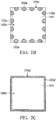
- the first patterned conductive patterned layer 102 may include a plurality of first conductors 102a disposed in and along the edge region 100a' of the package substrate 100. Moreover, the edge region 100a' is partially exposed from the plurality of first conductors 102a, as viewed from a top-view perspective.
- the first conductors 102a are L-shaped metal layers that are arranged at corners of the edge region 100a' and spaced apart from each other.
- the first conductors 102a spaced apart from each other are bar-shaped metal layers that are arranged at four sides of the edge region 100a' and the edge region 100a' corresponding to corners of the device region 100b are exposed from the bar-shaped metal layers, as viewed from a top-view perspective.
- the first conductors 102a of the first patterned conductive layer 102 are metal vias that are spaced apart from each other and the edge region 100a' corresponding to corners of the device region 100b are exposed from the metal vias (i.e., the first conductors 102a), as viewed from a top-view perspective.
- the first patterned conductive patterned layer 102 in the uppermost layer-level of the insulating layer 103 and adjacent to the first surface 101a includes a conductive continuous layer 102a' (e.g., a metal ring) in and extending along the edge region 100a', so as to surround the device region 100b without exposing the edge region 100a' corresponding to corners of the device region 100b, as viewed from a top-view perspective.
- a conductive continuous layer 102a' e.g., a metal ring
- the semiconductor package structure 10 further includes one or more semiconductor devices mounted onto the first surface 101a of the package substrate 100 and corresponding to the device region 100b of the package substrate 100.
- the semiconductor devices may include semiconductor dies 110 and 114 that are disposed on the first surface 101 of the package substrate 100.
- the semiconductor die 110 or 114 may include a microcontroller (MCU), a microprocessor (MPU), a random access memory (RAM), a base-band device, an artificial intelligence processing unit(APU), a power management integrated circuit (PMIC), a flash memory, a global positioning system (GPS) device, or a radio frequency (RF) device or any combination thereof.
- MCU microcontroller
- MPU microprocessor
- RAM random access memory
- APU artificial intelligence processing unit
- PMIC power management integrated circuit
- flash memory a flash memory
- GPS global positioning system
- RF radio frequency
- At least one of the semiconductor dies 110 and 114 is a SOC die.
- the semiconductor dies 110 and 114 are SOC dies.
- the semiconductor die 110 is a SOC die
- the semiconductor die 114 is a memory die.
- the semiconductor die 110 is a SOC die
- the semiconductor die 114 is a base-band die.
- the number and the arrangement of semiconductor dies are not limited to the disclosed embodiment.
- the semiconductor dies 110 and 114 are electrically connected to the package substrate 100. As shown in FIG. 1 , the semiconductor dies 110 and 114 are fabricated by flip-chip technology. The semiconductor dies 110 and 114 includes pads (not shown) are in contact with the corresponding conductive structures 112 and 116 (for example, conductive bumps, posts or solder pastes), respectively. It should be noted that the number of semiconductor dies integrated in the semiconductor package structure 10 is not limited to that disclosed in the embodiment. The pads of the semiconductor dies 110 and 114 are mounted onto the first patterned conductive layer 102 of the package substrate 100 via conductive structures 110 and 116, respectively.
- the semiconductor package structure 10 further includes one or more electronic components 120 mounted onto the first surface 101a of the package substrate 100 and corresponding to the device region 100b of the package substrate 100.
- the electronic component 120 may include a passive device that is electrically coupled to the semiconductor die 110 or 114 through the conductive traces of the package substrate 100.
- the passive device includes a capacitor, an inductor, a resistor, or a combination thereof.
- the passive device includes at least one electrode 122 electrically coupled to the first conductive patterned layer 102.
- the passive device may be a capacitor that includes electrode layers 122 respectively electrically coupled to the semiconductor die 110 through the first patterned conductive layer 102 of the package substrate 100.
- the semiconductor package structure 10 further includes an encapsulating layer 130a, covering the first surface 101a of the package substrate 100, corresponding to the device region 100b of the package substrate 100, and surrounding the semiconductor dies 110 and 114 and the electronic component 120.
- the encapsulating layer 130a may be formed of a molding compound layer, such as an epoxy, a resin, a moldable polymer, or the like.
- an optional underfill material (not shown) is disposed in the gaps between the conductive structures 112 and 116 and surrounded by the encapsulating layer 130a.
- the semiconductor package structure 10 further includes a conductive shielding layer 140, such as a metal layer, covering and surrounding the encapsulating layer 130a and electrically connected to the first conductors 102a shown in FIGS. 1, 2A and 2B (or the conductive continuous layer 102a, as shown in FIG. 2C ), so as to serve as an EMI shielding layer.
- a conductive shielding layer 140 such as a metal layer, covering and surrounding the encapsulating layer 130a and electrically connected to the first conductors 102a shown in FIGS. 1, 2A and 2B (or the conductive continuous layer 102a, as shown in FIG. 2C ), so as to serve as an EMI shielding layer.
- the first conductors 102a or the conductive continuous layer 102a are connected to ground and have a top surface in direct contact with the conductive shielding layer 140.
- the top surface of the first conductors 102a or of the conductive continuous layer 102a is substantially level with the first surface 101a of the package substrate 100, so that the sidewalls 101c of the package substrate 100 are entirely exposed from the conductive shielding layer 140, as shown in FIG. 1 . Namely, the sidewalls 101c of the package substrate 100 are not covered by the conductive shielding layer 140.
- the first patterned conductive layer 102 having first conductors 102a or a conductive continuous layer 102a is embedded in a layer-level of the insulating layer 103 below the first surface 101a, so that the conductive shielding layer 140 extends to and the covers the sidewalls of the package substrate 100 above the top surface of the first conductors 102a or the conductive continuous layer 102a.
- the first patterned conductive layer 102 does not have the first conductors 102a or the conductive continuous layer 102a and one of the second and third patterned conductive layers 104 and 106 has conductors or a conductive continuous layer with a structure and arrangement that are similar to those of the first conductors 102a or the conductive continuous layer 102a.
- the conductors or the conductive continuous layer also has a top surface in direct contact with the conductive shielding layer 140, so that the conductive shielding layer 140 extends to and the covers sidewalls of the package substrate 100 above the top surface of those conductors.
- the encapsulating layer 130a has tapered sidewalls 135. Moreover, portions of the conductive shielding layer 140 that surround the tapered sidewalls 135 of the encapsulating layer 130a have sidewalls 145 tiled with respect to sidewalls 101c of the package substrate 100, as shown in FIG. 1 .
- FIG. 3 is a cross-sectional view of an exemplary semiconductor package structure 20 in accordance with some embodiments of the disclosure.
- FIGS. 4A and 4B respectively show plan views of arrangements of first conductors and second conductors in the semiconductor package structure 20 in accordance with some embodiments of the disclosure.
- FIGS. 5A and 5B respectively show plan views of arrangements of first conductors and second conductors in the semiconductor package structure 20 in accordance with some embodiments of the disclosure. Descriptions of elements of the embodiments hereinafter that are the same as or similar to those previously described with reference to FIGS. 1, 2A , 2B, and 2C are omitted for brevity.
- the semiconductor package structure 20 is similar to the semiconductor package structure 10 shown in FIG. 1 .
- the second patterned conductive layer 104 of the semiconductor package structure 20 includes second conductors 104a disposed in and along the edge region 100a' of the package substrate 100. Moreover, the second conductors 104a are staggered with the first conductors 102a, as viewed from a top-view perspective.
- the first conductors 102a of the first patterned conductive layer 102 are bar-shaped metal layers that are spaced apart from each other and the edge region 100a' corresponding to corners of the device region 100b are exposed from the bar-shaped metal layers (i.e., the first conductors 102a), as viewed from a top-view perspective.
- the second conductors 104a of the second patterned conductive layer 104 include bar-shaped and L-shaped metal layers that are spaced apart from each other and located at the edge region 100a' exposed from the first conductors 102a, as viewed from a top-view perspective.
- the second conductors 104a are staggered with the first conductors 102a, as viewed from a top-view perspective. It should be noted that, although the first and second conductors 102a and 104a have a staggered arrangement, the first conductors 102a may partially overlap with the second conductors 104a, as viewed from a top-view perspective.
- first conductors 102a are arranged the same way as the second conductors 104a shown in FIG. 4B .
- second conductors 104a are arranged the same way as the first conductors 102a shown in FIG. 4A .
- the second patterned conductive layer 104 includes a conductive continuous layer (e.g., a metal ring) in and extending along the edge region 100a', so as to surround the device region 100b without exposing the edge region 100a' corresponding to corners of the device region 100b, as viewed from a top-view perspective.
- the first conductors 102a are arranged as shown in FIG. 4A , or in the same way as the second conductors 104a shown in FIG. 4B .
- the first conductors 102a of the first patterned conductive layer 102 and the second conductors 104a of the second patterned conductive layer 104 are metal vias that are spaced apart from each other.
- the arrangements of the first conductors 102a and the second conductors 104a may be similar to those of the first conductors 102a and the second conductors 104a shown in FIG. 4A and 4B , so that the second conductors 104a are staggered with the first conductors 102a, as viewed from a top-view perspective.
- the first conductors 102a are arranged the same way as the second conductors 104a. shown in FIG. 5B .
- the second conductors 104a are arranged the same way as the first conductors 102a shown in FIG. 5A .
- the second conductors 104a has a top surface in direct contact with the conductive shielding layer 140, so that the conductive shielding layer 140 also covers sidewalls 101c of the package substrate 100 above the top surface of the second conductors 104a.
- the first conductors 102a or the second conductors 104a may be connected to ground.
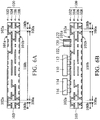
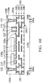
- FIGS. 6A to 6E are cross-sectional views of an exemplary method for forming the semiconductor package structure 10 shown in FIG. 1 , in accordance with some embodiments of the disclosure. Descriptions of elements of the embodiments hereinafter that are the same as or similar to those previously described with reference to FIGS. 1, 2A and 2B are omitted for brevity.
- a package substrate 100 is provided.
- the package substrate 100 has a first surface 101a and a second surface 101b opposite to the first surface 101a.
- the package substrate 100 has a scribe line region 100a and device regions 100b defined by the scribe line region 100a, so that those device regions 100b are surrounded by the scribe line region 100a. In order to simplify the diagram, only one entire device region 100b and two adjacent and partial device regions 100b are depicted.
- the package substrate 100 may include an insulating layer 103 (e.g., an inter-metal dielectric (IMD) layer).
- IMD inter-metal dielectric
- a first conductive patterned layer 102, a second conductive patterned layer 104, a third conductive patterned layer 106, and a fourth conductive patterned layer 108 are respectively disposed in a first layer-level, a second layer-level, a third layer-level, and a fourth layer-level of the insulating layer 103.
- the number of patterned conductive layers shown in FIG. 6A is only an example and is not a limitation to the present invention.
- the first conductive patterned layer 102 may include first conductors 102a disposed in and along the scribe line region 100a or include a conductive continuous layer (not shown) in and extending along the scribe line region 100a.
- the first conductors 102a may bridge the first conductive patterned layers 102 disposed in adjacent device regions 100b of the package substrate 100.
- the shape, the structure, and the arrangement of the first conductors 102a in the scribe line region 100a are the same as or similar to those of the first conductors 102a in the edge region 100a' shown in FIG. 2A or 2B .
- the scribe line region 100a is partially exposed from the first conductors 102a, as viewed from a top-view perspective.
- the exposed scribe line region 100a (e.g., the portions of the scribe line region 100a corresponding to corners of each device region 100b) may serve as a buffer region for stress release.
- the shape, the structure, and the arrangement of the conductive continuous layer are the same as or similar to those of the conductive continuous layer 102a' in the edge region 100a' shown in FIG. 2C .
- one or more semiconductor devices such as semiconductor dies 110 and 114, and one or more electronic components 120 such as passive devices are mounted onto each device region 100b of the package substrate 100 by one or more bonding processes.
- the package substrate 100 having the semiconductor dies 110 and 114 and the electronic component 120 thereon is covered with an encapsulating material 130.
- the encapsulating material 130 may be formed of a molding compound layer, such as an epoxy, a resin, a moldable polymer, or the like, and formed by a molded underfill (MUF) process.
- the encapsulating material 130 may be applied while it is substantially liquid, and then may be cured through a chemical reaction, such as in an epoxy or resin.
- the encapsulating material 130 may be an ultraviolet (UV) or thermally cured polymer applied as a gel or malleable solid capable of being disposed around the first semiconductor die 110, and then may be cured through a UV or thermal curing process.
- the encapsulating material 130 may be cured with a mold (not shown).
- the encapsulating material 130 may be formed by a capillary underfill (CUF) process, so that an underfill material (not shown) is disposed in the gaps between the conductive structures 112 of the semiconductor die 110 and the conductive structures 116 of the semiconductor die 114 and surrounded by the encapsulating material 130.
- UV ultraviolet
- CRF capillary underfill
- an opening 132 is formed in the encapsulating material 130 to expose the scribe line region 100a of the package substrate 100, thereby separating the encapsulating material 130 into encapsulating layers 130a that correspond to the device regions 100b and are spaced apart from each other.
- the opening 132 is formed by a laser ablation process, so that the formed encapsulating layer 130a has tapered sidewalls 135.
- the opening 132 has a bottom that is substantially level with the first surface 101a of the package substrate 100 or the interface between the package substrate 100 and the encapsulating layer 130a, so that the first conductors 102a or the conductive continuous layer in the scribe line region 100a of the package substrate 100 are also exposed by the opening 132.
- the first patterned conductive layer 102 having first conductors 102a or a conductive continuous layer is embedded in a layer-level of the insulating layer 103 below the first surface 101a.
- the opening 132 that is formed may extend into the insulating layer 103, thereby exposing the first conductors 102a or the conductive continuous layer.
- a conductive shielding layer 140 such as a metal layer (e.g., copper or stainless steel), is formed on the encapsulating layers 130a and conformally fills the opening 132 by, for example, a sputtering process, so as to be electrically connected to the first conductors 102a or the conductive continuous layer exposed by the opening 132.
- the conductive shielding layer 140 may be in direct contact with the top surface of the first conductors 102a or the conductive continuous layer through the opening 132, so as to serve as an EMI shielding layer.
- a singulation process is performed by cutting the scribe line region 100a of the package substrate 100 through the opening 132, so as to form semiconductor package structures 10 (as shown in FIG. 1 ).
- a conductive bump structure (not shown), such as a copper bump or a solder bump structure, a conductive pillar structure, a conductive wire structure, or a conductive paste structure may be formed on the second surface 101b of the package substrate 100 prior to the singulation process.
- the methods for forming the semiconductor package structure 20 shown in FIG. 3 can be the same as or similar to the methods shown in FIGS. 6A to 6E .
- the second patterned conductive layer 104 in the package substrate 100 may include second conductors 104a in and along the scribe line region 100a.
- the second conductors 104a are staggered with the first conductors 102a, as viewed from a top-view perspective.
- the shape, the structure, and the arrangement of the first conductors 102a in the scribe line region 100a are the same as or similar to those of the first conductors 102a in the edge region 100a' shown in FIG.
- the scribe line region 100a is partially exposed from the first conductors 102a, as viewed from a top-view perspective.
- the scribe line region 100a corresponding to corners of each device region 100b is exposed from the corresponding first conductors 102a, as viewed from a top-view perspective.
- the second conductors 104a may serve as a reflect layer or a resist layer during performing a laser ablation process that is used for forming the opening in the encapsulating material and extending into the package substrate 100, so as to expose the second conductors 104a.
- the shape, the structure, and the arrangement of the first conductors 102a in the scribe line region 100a are the same as or similar to those of the first conductors 102a in the edge region 100a' shown in FIG. 5A and the shape, the structure, and the arrangement of the second conductors 104a in the scribe line region 100a are the same as or similar to those of the second conductors 104a in the edge region 100a' shown in FIG. 5B .
- the opening formed in the encapsulating material extends into the insulating layer 103, so that the second conductors 104a have a top surface that is in direct contact with the conductive shielding layer 140 through the opening.
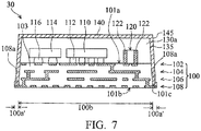
- FIG. 7 is a cross-sectional view of an exemplary semiconductor package structure 30 in accordance with some embodiments of the disclosure. Descriptions of elements of the embodiments hereinafter that are the same as or similar to those previously described with reference to FIG. 1 are omitted for brevity.
- the semiconductor package structure 30 is similar to the semiconductor package structure 10 shown in FIG. 1 . The difference is the first patterned conductive layer 102 does not have the first conductors 102a. However, the fourth patterned conductive patterned layer 108 may include a plurality of fourth conductors 108a disposed in and along the edge region 100a' of the package substrate 100.
- the conductive shielding layer 140 such as a metal layer, covering and surrounding the encapsulating layer 130a and electrically connected to the fourth conductors 108a shown in FIGS. 7 (or a conductive continuous layer 108a), so as to serve as an EMI shielding layer.
- the fourth conductors 108a or the conductive continuous layer 108a are connected to ground and have a top surface in direct contact with the conductive shielding layer 140.
- the sidewalls 101c of the package substrate 100 are entirely or partially wished by the conductive shielding layer 140, as shown in FIG. 7 .
- the shape, the structure, and the arrangement of the fourth conductors 108a in the edge region 100a' are the same as or similar to those of the first conductors 102a in the edge region 100a' shown in FIG. 2A or 2B .
- the edge region 100 a' is partially exposed from the plurality of fourth conductors 108a, as viewed from a top-view perspective.
- the fourth patterned conductive patterned layer 108 may include a conductive continuous layer (not shown) and the shape, the structure, and the arrangement of the conductive continuous layer in the edge region 100 a' are the same as or similar to those of the second conductors 104a in the edge region 100a' shown in FIG. 2C .
- the methods for forming the semiconductor package structure 30 shown in FIG. 7 can be the same as or similar to the methods shown in FIGS. 6A to 6E .
- the fourth patterned conductive layer 108 in the package substrate 100 may include fourth conductors 108a or a conductive continuous layer in and along the scribe line region of the package substrate 100.
- the opening formed in the encapsulating material extends into the insulating layer 103, so that the fourth conductors 108a has a top surface in direct contact with the conductive shielding layer 140 through the opening.
- FIG. 8 is a cross-sectional view of an exemplary semiconductor package structure 40 in accordance with some embodiments of the disclosure. Descriptions of elements of the embodiments hereinafter that are the same as or similar to those previously described with reference to FIG. 1 are omitted for brevity.
- the semiconductor package structure 40 is similar to the semiconductor package structure 10 shown in FIG. 1 . The difference is portions of the conductive shielding layer 140 that surround the sidewalls 135 of the encapsulating layer 130a have sidewalls 145 that are substantially level with those of the package substrate 100.
- the methods for forming the semiconductor package structure 40 shown in FIG. 8 can be the same as or similar to the methods shown in FIGS. 6A to 6E .
- the opening formed in the encapsulating material 130 may be entirely filled with the conductive shielding layer 140, so that portions of the conductive shielding layer 140 that surround the sidewalls 135 of the encapsulating layer 130a have sidewalls 145 that are substantially level with those of the package substrate 100 after the singulation process has been performed.
- the conductive shielding layer 140 may be formed by a plating process or a spray deposition process.
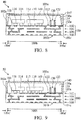
- FIG. 9 is a cross-sectional view of an exemplary semiconductor package structure 50 in accordance with some embodiments of the disclosure. Descriptions of elements of the embodiments hereinafter that are the same as or similar to those previously described with reference to FIG. 8 are omitted for brevity.
- the semiconductor package structure 50 is similar to the semiconductor package structure 40 shown in FIG. 8 . The difference is the encapsulating layer 130a has sidewalls 135 that are substantially vertical.
- the methods for forming the semiconductor package structure 50 shown in FIG. 9 can be the same as or similar to the methods shown in FIGS. 6A to 6E .
- the opening in the encapsulating material 130 may be formed by a blade sawing process, so that the formed encapsulating layer 130a has sidewalls 135 that are substantially vertical after the singulation process has been performed.
- the conductive shielding layer 140 may be formed by a plating process or a spray deposition process.
- FIG. 10 is a cross-sectional view of an exemplary semiconductor package structure 60 in accordance with some embodiments of the disclosure. Descriptions of elements of the embodiments hereinafter that are the same as or similar to those previously described with reference to FIG. 8 are omitted for brevity.
- the semiconductor package structure 60 is similar to the semiconductor package structure 40 shown in FIG. 8 . The difference is the semiconductor package structure 60 further includes a heat spreader 160 over the conductive shielding layer 140. In some embodiments, the heat spreader 160 is formed over the conductive shielding layer 140 via an attached film 150.
- the methods for forming the semiconductor package structure 60 shown in FIG. 10 can be the same as or similar to the methods shown in FIGS. 6A to 6E .
- the attached film 150 and the heat spreader 160 are successively formed on the conductive shielding layer 140, so that the heat spreader 160 is attached onto the conductive shielding layer 140.
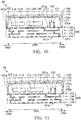
- FIG. 11 is a cross-sectional view of an exemplary semiconductor package structure 70 in accordance with some embodiments of the disclosure. Descriptions of elements of the embodiments hereinafter that are the same as or similar to those previously described with reference to FIG. 9 are omitted for brevity.
- the semiconductor package structure 70 is similar to the semiconductor package structure 50 shown in FIG. 9 . The difference is the semiconductor package structure 70 further includes a heat spreader 160 over the conductive shielding layer 140. In some embodiments, the heat spreader 160 is formed over the conductive shielding layer 140 via an attached film 150.
- the methods for forming the semiconductor package structure 70 shown in FIG. 11 can be the same as or similar to the methods shown in FIGS. 6A to 6E .
- the attached film 150 and the heat spreader 160 are successively formed on the conductive shielding layer 140, so that the heat spreader 160 is attached onto the conductive shielding layer 140.
- package substrate 100 shown in FIGS. 8, 9 , 10, and 11 can be replaced by package substrate 100 shown in FIG. 3 .
- the semiconductor package structure is designed to fabricate an EMI shielding layer integrated into the semiconductor package(s).
- the EMI shielding layer provides the function of reducing electrical noise and electromagnetic radiation and a compatible process for the semiconductor package structure. Accordingly, there is no need to perform an additional process for forming the shielding device. As a result, reliability, yield, and throughput of the semiconductor package structure are increased and the manufacturing cost of the semiconductor package structure is reduced.
- the integrated EMI shielding layer can provide design flexibility for the system integration of the semiconductor package structure. Moreover, the thickness of the EMI shielding layer formed by metal sputtering, plating, or spray deposition can be reduced, thereby reducing the size of the semiconductor package structure and preventing package warpage and delamination of the EMI shielding layer.
- the conductive continuous layer/the conductors formed in the scribe line region of the package substrate is/are exposed prior to the singulation process, so that the EMI shielding layer can also be formed prior to the singulation process. Since the EMI shielding layer is formed prior to the singulation process, additional tape mounting process and package rearrangement in the conventional fabrication for the EMI shielding can be omitted, thereby reducing the manufacturing cost and the process time for the semiconductor package structure and preventing pad of the package substrate from being contaminated due to the tape mounting process.
Landscapes
- Structures Or Materials For Encapsulating Or Coating Semiconductor Devices Or Solid State Devices (AREA)
- Physics & Mathematics (AREA)
- Health & Medical Sciences (AREA)
- Electromagnetism (AREA)
- Toxicology (AREA)
- Geometry (AREA)
- Engineering & Computer Science (AREA)
- Microelectronics & Electronic Packaging (AREA)
Abstract
Description
- This application claims the benefit of
U.S. Provisional Application No. 62/531,912 filed on July 13, 2017 - The present invention relates to a semiconductor package, and in particular to a semiconductor package that includes an EMI shielding structure.
- In order to ensure the continued miniaturization and multi-functionality of electronic products and communication devices, it is desired that semiconductor packages be small in size, support multi-pin connection, operate at high speeds, and have high functionality.
- In such semiconductor packages, the integrated circuit chips incorporated therein may be subject to disturbance by electromagnetic interference (EMI). EMI may cause the semiconductor packages to exhibit abnormal operation and poor performance. To shield the semiconductor package from EMI, a metal shielding layer is embedded in an encapsulant of the semiconductor package. However, once fabrication is complicated, package thickness is increased, package warpage may occur, and the shielding layer may become delaminated when the shielding layer is embedded in the structure of the semiconductor package.
- Another approach to EMI shielding is to coat a metal on the surface of the encapsulant of the semiconductor package. However, since the metal is typically formed after a singulation process, the package structure is not suitable for mass production.
- Thus, a novel semiconductor package structure is desirable.
- Semiconductor package structures are provided. An exemplary embodiment of a semiconductor package structure includes an encapsulating layer and a package substrate having a device region covered by the encapsulating layer and an edge region surrounding the device region and exposed from the encapsulating layer. The package substrate includes an insulating layer and a first patterned conductive layer in a first layer-level of the insulating layer. The package substrate includes a plurality of first conductors in and along the edge region. The edge region is partially exposed from the plurality of first conductors, as viewed from a top-view perspective. A semiconductor die is disposed on the device region of the package substrate and surrounded by the encapsulating layer. A conductive shielding layer covers and surrounds the encapsulating layer and electrically connected to the plurality of first conductors.
- Another exemplary embodiment of a semiconductor package structure includes an encapsulating layer and a package substrate having a device region covered by the encapsulating layer and an edge region surrounding the device region and exposed from the encapsulating layer. The package substrate includes an insulating layer and a first patterned conductive layer in a first layer-level of the insulating layer. The first patterned conductive layer includes a conductive continuous layer in and extending along the edge region. A semiconductor die is disposed on the device region of the package substrate and surrounded by the encapsulating layer. A conductive shielding layer covers and surrounds the encapsulating layer and is electrically connected to the conductive continuous layer.
- An exemplary embodiment of a method for forming a semiconductor package structure includes providing a package substrate having a scribe line region and a plurality of device regions defined by the scribe line region. The package substrate includes an insulating layer and a first patterned conductive layer in a first layer-level of the insulating layer. The first patterned conductive layer includes a plurality of first conductors in and along the scribe line region. The scribe line region is partially exposed from the plurality of first conductors, as viewed from a top-view perspective. A semiconductor die is mounted onto each of the plurality of device regions of the package substrate. The package substrate is covered with an encapsulating material. An opening is formed in the encapsulating material to expose the scribe line region of the package substrate and form a plurality of encapsulating layers corresponding to the plurality of device regions. A conductive shielding layer is formed on the plurality of encapsulating layers and fills the opening, so as to be electrically connected to the plurality of first conductors.
- A detailed description is given in the following embodiments with reference to the accompanying drawings.
- The present invention can be more fully understood by reading the subsequent detailed description and examples with references made to the accompanying drawings, wherein:
-
FIG. 1 is a cross-sectional view of an exemplary semiconductor package structure in accordance with some embodiments of the disclosure. -
FIG. 2A is a plan view of the arrangement of first conductors in the semiconductor package structure in accordance with some embodiments of the disclosure. -
FIG. 2B is a plan view of the arrangement of first conductors in the semiconductor package structure in accordance with some embodiments of the disclosure. -
FIG. 2C is a plan view of a conductive continuous layer in the semiconductor package structure in accordance with some embodiments of the disclosure. -
FIG. 3 is a cross-sectional view of an exemplary semiconductor package structure in accordance with some embodiments of the disclosure. -
FIG. 4A is a plan view of the arrangement of first conductors in the semiconductor package structure in accordance with some embodiments of the disclosure. -
FIG. 4B is a plan view of the arrangement of second conductors in the semiconductor package structure in accordance with some embodiments of the disclosure. -
FIG. 5A is a plan view of the arrangement of first conductors in the semiconductor package structure in accordance with some embodiments of the disclosure. -
FIG. 5B is a plan view of the arrangement of second conductors in the semiconductor package structure in accordance with some embodiments of the disclosure. -
FIGS. 6A to 6E are cross-sectional views of an exemplary method for forming a semiconductor package structure in accordance with some embodiments of the disclosure. -
FIG. 7 is a cross-sectional view of an exemplary semiconductor package structure in accordance with some embodiments of the disclosure. -
FIG. 8 is a cross-sectional view of an exemplary semiconductor package structure in accordance with some embodiments of the disclosure. -
FIG. 9 is a cross-sectional view of an exemplary semiconductor package structure in accordance with some embodiments of the disclosure. -
FIG. 10 is a cross-sectional view of an exemplary semiconductor package structure in accordance with some embodiments of the disclosure. -
FIG. 11 is a cross-sectional view of an exemplary semiconductor package structure in accordance with some embodiments of the disclosure. - The following description is of the best-contemplated mode of carrying out the invention. This description is made for the purpose of illustrating the general principles of the invention and should not be taken in a limiting sense. The scope of the invention is determined by reference to the appended claims.
- The present invention will be described with respect to particular embodiments and with reference to certain drawings, but the invention is not limited thereto and is only limited by the claims. The drawings described are only schematic and are non-limiting. In the drawings, the size of some of the elements may be exaggerated for illustrative purposes and not drawn to scale. The dimensions and the relative dimensions do not correspond to actual dimensions in the practice of the invention.
-
FIG. 1 is a cross-sectional view of an exemplarysemiconductor package structure 10 in accordance with some embodiments of the disclosure.FIGS. 2A ,2B and 2C are plan views of various arrangements of first conductors in thesemiconductor package structure 10 in accordance with some embodiments of the disclosure. In some embodiments, thesemiconductor package structure 10 is a wafer-level semiconductor package structure, for example, a flip-chip semiconductor package structure. - Referring to
FIG. 1 , thesemiconductor package structure 10 may be mounted on a base (not shown). In some embodiments, thesemiconductor package structure 10 may include a system-on-chip (SOC) package structure. Moreover, the base may include a printed circuit board (PCB) and may be formed of polypropylene (PP). In some embodiments, thesemiconductor package structure 10 is mounted on the base by a bonding process. For example, thesemiconductor package structure 10 may include a conductive bump structure (not shown), such as a copper bump or a solder bump structure, a conductive pillar structure, a conductive wire structure, or a conductive paste structure that may be mounted on and electrically coupled to the base by the bonding process. - The
semiconductor package structure 10 includes apackage substrate 100 having adevice region 100b and anedge region 100a' surrounding thedevice region 100b. Moreover, thepackage substrate 100 has afirst surface 101a and asecond surface 101b opposite to thefirst surface 101a. - In some embodiments, the
package substrate 100 includes a redistribution layer (RDL) structure (which is also referred to as a fan-out structure) therein. In some embodiments, thepackage substrate 100 includes an insulating layer 103 (e.g., an inter-metal dielectric (IMD) layer) and one or more patterned conductive layers serving as conductive traces and disposed in the insulatinglayer 103. For example, a first conductive patternedlayer 102 is disposed in a first layer-level of the insulatinglayer 103. Moreover, a second conductive patternedlayer 104 is disposed in a second layer-level of the insulatinglayer 103 lower than the first layer-level. A third conductive patternedlayer 106 is disposed in a third layer-level of the insulatinglayer 103 lower than the second layer-level and a fourth conductive patternedlayer 108 is disposed in a fourth layer-level of the insulatinglayer 103 lower than the third layer-level. Those conductive patterned layer may be formed of metal. In some embodiments, the insulating layer 103 (i.e., the IMD layer) may include sub-dielectric layers successively stacked from thesecond surface 101b of thepackage substrate 100 toward thefirst surface 101a of thepackage substrate 100. In some embodiments, the insulatinglayer 103 may be formed of organic materials, which include a polymer base material, non-organic materials, which include silicon nitride (SiNx), silicon oxide (SiOx), or the like. For example, those sub-dielectric layers are made of a polymer base material. In some embodiments, the insulatinglayer 103 is a high-k dielectric layer (k is the dielectric constant of the dielectric layer). It should be noted that the number of patterned conductive layers and the number of sub-dielectric layers of thepackage substrate 100 shown inFIG. 1 is only an example and is not a limitation to the present invention. - In some embodiments, the first patterned conductive patterned
layer 102 is in the uppermost layer-level of the insulatinglayer 103 and adjacent to thefirst surface 101a, so that the first patterned conductive patternedlayer 102 has a top surface that is substantially level with thefirst surface 101a. The first patterned conductive patternedlayer 102 may include a plurality offirst conductors 102a disposed in and along theedge region 100a' of thepackage substrate 100. Moreover, theedge region 100a' is partially exposed from the plurality offirst conductors 102a, as viewed from a top-view perspective. - For example, as shown in 2A, the
first conductors 102a are L-shaped metal layers that are arranged at corners of theedge region 100a' and spaced apart from each other. Alternatively, thefirst conductors 102a spaced apart from each other are bar-shaped metal layers that are arranged at four sides of theedge region 100a' and theedge region 100a' corresponding to corners of thedevice region 100b are exposed from the bar-shaped metal layers, as viewed from a top-view perspective. - In some embodiments, as shown in
FIG. 2B , thefirst conductors 102a of the first patternedconductive layer 102 are metal vias that are spaced apart from each other and theedge region 100a' corresponding to corners of thedevice region 100b are exposed from the metal vias (i.e., thefirst conductors 102a), as viewed from a top-view perspective. - In some embodiments, as shown in
FIG. 2C , the first patterned conductive patternedlayer 102 in the uppermost layer-level of the insulatinglayer 103 and adjacent to thefirst surface 101a includes a conductivecontinuous layer 102a' (e.g., a metal ring) in and extending along theedge region 100a', so as to surround thedevice region 100b without exposing theedge region 100a' corresponding to corners of thedevice region 100b, as viewed from a top-view perspective. - In some embodiments, the
semiconductor package structure 10 further includes one or more semiconductor devices mounted onto thefirst surface 101a of thepackage substrate 100 and corresponding to thedevice region 100b of thepackage substrate 100. In some embodiments, the semiconductor devices may include semiconductor dies 110 and 114 that are disposed on the first surface 101 of thepackage substrate 100. In some embodiments, the semiconductor die 110 or 114 may include a microcontroller (MCU), a microprocessor (MPU), a random access memory (RAM), a base-band device, an artificial intelligence processing unit(APU), a power management integrated circuit (PMIC), a flash memory, a global positioning system (GPS) device, or a radio frequency (RF) device or any combination thereof. In some embodiments, at least one of the semiconductor dies 110 and 114 is a SOC die. For example, the semiconductor dies 110 and 114 are SOC dies. Alternatively, the semiconductor die 110 is a SOC die, and the semiconductor die 114 is a memory die. In some other embodiments, the semiconductor die 110 is a SOC die, and the semiconductor die 114 is a base-band die. However, the number and the arrangement of semiconductor dies are not limited to the disclosed embodiment. - In some embodiments, the semiconductor dies 110 and 114 are electrically connected to the
package substrate 100. As shown inFIG. 1 , the semiconductor dies 110 and 114 are fabricated by flip-chip technology. The semiconductor dies 110 and 114 includes pads (not shown) are in contact with the correspondingconductive structures 112 and 116 (for example, conductive bumps, posts or solder pastes), respectively. It should be noted that the number of semiconductor dies integrated in thesemiconductor package structure 10 is not limited to that disclosed in the embodiment. The pads of the semiconductor dies 110 and 114 are mounted onto the first patternedconductive layer 102 of thepackage substrate 100 viaconductive structures - In some embodiments, the
semiconductor package structure 10 further includes one or moreelectronic components 120 mounted onto thefirst surface 101a of thepackage substrate 100 and corresponding to thedevice region 100b of thepackage substrate 100. In some embodiments, theelectronic component 120 may include a passive device that is electrically coupled to the semiconductor die 110 or 114 through the conductive traces of thepackage substrate 100. In some embodiments, the passive device includes a capacitor, an inductor, a resistor, or a combination thereof. Moreover, the passive device includes at least oneelectrode 122 electrically coupled to the first conductive patternedlayer 102. For example, the passive device may be a capacitor that includes electrode layers 122 respectively electrically coupled to the semiconductor die 110 through the first patternedconductive layer 102 of thepackage substrate 100. - In some embodiments, the
semiconductor package structure 10 further includes anencapsulating layer 130a, covering thefirst surface 101a of thepackage substrate 100, corresponding to thedevice region 100b of thepackage substrate 100, and surrounding the semiconductor dies 110 and 114 and theelectronic component 120. In some embodiments, theencapsulating layer 130a may be formed of a molding compound layer, such as an epoxy, a resin, a moldable polymer, or the like. In some embodiments, an optional underfill material (not shown) is disposed in the gaps between theconductive structures encapsulating layer 130a. - In some embodiments, the
semiconductor package structure 10 further includes aconductive shielding layer 140, such as a metal layer, covering and surrounding theencapsulating layer 130a and electrically connected to thefirst conductors 102a shown inFIGS. 1, 2A and2B (or the conductivecontinuous layer 102a, as shown inFIG. 2C ), so as to serve as an EMI shielding layer. In such cases, thefirst conductors 102a or the conductivecontinuous layer 102a are connected to ground and have a top surface in direct contact with theconductive shielding layer 140. In some embodiments, the top surface of thefirst conductors 102a or of the conductivecontinuous layer 102a is substantially level with thefirst surface 101a of thepackage substrate 100, so that the sidewalls 101c of thepackage substrate 100 are entirely exposed from theconductive shielding layer 140, as shown inFIG. 1 . Namely, the sidewalls 101c of thepackage substrate 100 are not covered by theconductive shielding layer 140. Alternatively, the first patternedconductive layer 102 havingfirst conductors 102a or a conductivecontinuous layer 102a is embedded in a layer-level of the insulatinglayer 103 below thefirst surface 101a, so that theconductive shielding layer 140 extends to and the covers the sidewalls of thepackage substrate 100 above the top surface of thefirst conductors 102a or the conductivecontinuous layer 102a. - In some other embodiments, the first patterned
conductive layer 102 does not have thefirst conductors 102a or the conductivecontinuous layer 102a and one of the second and third patternedconductive layers first conductors 102a or the conductivecontinuous layer 102a. Similarly, the conductors or the conductive continuous layer also has a top surface in direct contact with theconductive shielding layer 140, so that theconductive shielding layer 140 extends to and the covers sidewalls of thepackage substrate 100 above the top surface of those conductors. - In some embodiments, the
encapsulating layer 130a has taperedsidewalls 135. Moreover, portions of theconductive shielding layer 140 that surround the tapered sidewalls 135 of theencapsulating layer 130a have sidewalls 145 tiled with respect tosidewalls 101c of thepackage substrate 100, as shown inFIG. 1 . -
FIG. 3 is a cross-sectional view of an exemplarysemiconductor package structure 20 in accordance with some embodiments of the disclosure.FIGS. 4A and 4B respectively show plan views of arrangements of first conductors and second conductors in thesemiconductor package structure 20 in accordance with some embodiments of the disclosure.FIGS. 5A and 5B respectively show plan views of arrangements of first conductors and second conductors in thesemiconductor package structure 20 in accordance with some embodiments of the disclosure. Descriptions of elements of the embodiments hereinafter that are the same as or similar to those previously described with reference toFIGS. 1, 2A ,2B, and 2C are omitted for brevity. Referring toFIG. 3 , thesemiconductor package structure 20 is similar to thesemiconductor package structure 10 shown inFIG. 1 . Unlike thesemiconductor package structure 10 shown inFIG. 1 , the second patternedconductive layer 104 of thesemiconductor package structure 20 includessecond conductors 104a disposed in and along theedge region 100a' of thepackage substrate 100. Moreover, thesecond conductors 104a are staggered with thefirst conductors 102a, as viewed from a top-view perspective. - In some embodiments, as shown in
FIGS. 4A and 4B , thefirst conductors 102a of the first patternedconductive layer 102 are bar-shaped metal layers that are spaced apart from each other and theedge region 100a' corresponding to corners of thedevice region 100b are exposed from the bar-shaped metal layers (i.e., thefirst conductors 102a), as viewed from a top-view perspective. Moreover, thesecond conductors 104a of the second patternedconductive layer 104 include bar-shaped and L-shaped metal layers that are spaced apart from each other and located at theedge region 100a' exposed from thefirst conductors 102a, as viewed from a top-view perspective. As a result, thesecond conductors 104a are staggered with thefirst conductors 102a, as viewed from a top-view perspective. It should be noted that, although the first andsecond conductors first conductors 102a may partially overlap with thesecond conductors 104a, as viewed from a top-view perspective. - Alternatively, the
first conductors 102a are arranged the same way as thesecond conductors 104a shown inFIG. 4B . In this embodiment, thesecond conductors 104a are arranged the same way as thefirst conductors 102a shown inFIG. 4A . - In some other embodiments, the second patterned
conductive layer 104 includes a conductive continuous layer (e.g., a metal ring) in and extending along theedge region 100a', so as to surround thedevice region 100b without exposing theedge region 100a' corresponding to corners of thedevice region 100b, as viewed from a top-view perspective. In such cases, thefirst conductors 102a are arranged as shown inFIG. 4A , or in the same way as thesecond conductors 104a shown inFIG. 4B . - In some embodiments, as shown in
FIGS. 5A and 5B , thefirst conductors 102a of the first patternedconductive layer 102 and thesecond conductors 104a of the second patternedconductive layer 104 are metal vias that are spaced apart from each other. As shown in FIS. 5A and 5B, the arrangements of thefirst conductors 102a and thesecond conductors 104a may be similar to those of thefirst conductors 102a and thesecond conductors 104a shown inFIG. 4A and 4B , so that thesecond conductors 104a are staggered with thefirst conductors 102a, as viewed from a top-view perspective. Alternatively, thefirst conductors 102a are arranged the same way as thesecond conductors 104a. shown inFIG. 5B . In this case, thesecond conductors 104a are arranged the same way as thefirst conductors 102a shown inFIG. 5A . - Although it is not shown in
FIG. 3 , similar to thefirst conductors 102a, thesecond conductors 104a has a top surface in direct contact with theconductive shielding layer 140, so that theconductive shielding layer 140 also coverssidewalls 101c of thepackage substrate 100 above the top surface of thesecond conductors 104a. Moreover, thefirst conductors 102a or thesecond conductors 104a may be connected to ground. -
FIGS. 6A to 6E are cross-sectional views of an exemplary method for forming thesemiconductor package structure 10 shown inFIG. 1 , in accordance with some embodiments of the disclosure. Descriptions of elements of the embodiments hereinafter that are the same as or similar to those previously described with reference toFIGS. 1, 2A and2B are omitted for brevity. Referring toFIG. 6A , apackage substrate 100 is provided. Thepackage substrate 100 has afirst surface 101a and asecond surface 101b opposite to thefirst surface 101a. Moreover, thepackage substrate 100 has ascribe line region 100a anddevice regions 100b defined by thescribe line region 100a, so that thosedevice regions 100b are surrounded by thescribe line region 100a. In order to simplify the diagram, only oneentire device region 100b and two adjacent andpartial device regions 100b are depicted. - The
package substrate 100 may include an insulating layer 103 (e.g., an inter-metal dielectric (IMD) layer). In some embodiments, a first conductive patternedlayer 102, a second conductive patternedlayer 104, a third conductive patternedlayer 106, and a fourth conductive patternedlayer 108 are respectively disposed in a first layer-level, a second layer-level, a third layer-level, and a fourth layer-level of the insulatinglayer 103. It should be noted that the number of patterned conductive layers shown inFIG. 6A is only an example and is not a limitation to the present invention. - The first conductive patterned
layer 102 may includefirst conductors 102a disposed in and along thescribe line region 100a or include a conductive continuous layer (not shown) in and extending along thescribe line region 100a. Thefirst conductors 102a may bridge the first conductivepatterned layers 102 disposed inadjacent device regions 100b of thepackage substrate 100. - For a
single device region 100b of thepackage substrate 100, the shape, the structure, and the arrangement of thefirst conductors 102a in thescribe line region 100a are the same as or similar to those of thefirst conductors 102a in theedge region 100a' shown inFIG. 2A or2B . As a result, thescribe line region 100a is partially exposed from thefirst conductors 102a, as viewed from a top-view perspective. The exposedscribe line region 100a (e.g., the portions of thescribe line region 100a corresponding to corners of eachdevice region 100b) may serve as a buffer region for stress release. - Also, the shape, the structure, and the arrangement of the conductive continuous layer are the same as or similar to those of the conductive
continuous layer 102a' in theedge region 100a' shown inFIG. 2C . - Referring to
FIG. 6B , one or more semiconductor devices such as semiconductor dies 110 and 114, and one or moreelectronic components 120 such as passive devices are mounted onto eachdevice region 100b of thepackage substrate 100 by one or more bonding processes. - Afterwards, as shown in
FIG. 6C , thepackage substrate 100 having the semiconductor dies 110 and 114 and theelectronic component 120 thereon is covered with an encapsulatingmaterial 130. In some embodiments, the encapsulatingmaterial 130 may be formed of a molding compound layer, such as an epoxy, a resin, a moldable polymer, or the like, and formed by a molded underfill (MUF) process. The encapsulatingmaterial 130 may be applied while it is substantially liquid, and then may be cured through a chemical reaction, such as in an epoxy or resin. In some other embodiments, the encapsulatingmaterial 130 may be an ultraviolet (UV) or thermally cured polymer applied as a gel or malleable solid capable of being disposed around the first semiconductor die 110, and then may be cured through a UV or thermal curing process. The encapsulatingmaterial 130 may be cured with a mold (not shown). In some embodiments, the encapsulatingmaterial 130 may be formed by a capillary underfill (CUF) process, so that an underfill material (not shown) is disposed in the gaps between theconductive structures 112 of the semiconductor die 110 and theconductive structures 116 of the semiconductor die 114 and surrounded by the encapsulatingmaterial 130. - Referring to
FIG. 6D , anopening 132 is formed in the encapsulatingmaterial 130 to expose thescribe line region 100a of thepackage substrate 100, thereby separating the encapsulatingmaterial 130 into encapsulatinglayers 130a that correspond to thedevice regions 100b and are spaced apart from each other. In some embodiments, theopening 132 is formed by a laser ablation process, so that the formedencapsulating layer 130a has taperedsidewalls 135. After the encapsulatingmaterial 130 is formed, theopening 132 has a bottom that is substantially level with thefirst surface 101a of thepackage substrate 100 or the interface between thepackage substrate 100 and theencapsulating layer 130a, so that thefirst conductors 102a or the conductive continuous layer in thescribe line region 100a of thepackage substrate 100 are also exposed by theopening 132. - In some embodiments, the first patterned
conductive layer 102 havingfirst conductors 102a or a conductive continuous layer is embedded in a layer-level of the insulatinglayer 103 below thefirst surface 101a. In such cases, theopening 132 that is formed may extend into the insulatinglayer 103, thereby exposing thefirst conductors 102a or the conductive continuous layer. - Referring to
FIG. 6E , after theopening 132 is formed, aconductive shielding layer 140, such as a metal layer (e.g., copper or stainless steel), is formed on the encapsulatinglayers 130a and conformally fills theopening 132 by, for example, a sputtering process, so as to be electrically connected to thefirst conductors 102a or the conductive continuous layer exposed by theopening 132. Theconductive shielding layer 140 may be in direct contact with the top surface of thefirst conductors 102a or the conductive continuous layer through theopening 132, so as to serve as an EMI shielding layer. - Afterwards, a singulation process is performed by cutting the
scribe line region 100a of thepackage substrate 100 through theopening 132, so as to form semiconductor package structures 10 (as shown inFIG. 1 ). In some embodiments, a conductive bump structure (not shown), such as a copper bump or a solder bump structure, a conductive pillar structure, a conductive wire structure, or a conductive paste structure may be formed on thesecond surface 101b of thepackage substrate 100 prior to the singulation process. - It should be understood that the methods for forming the
semiconductor package structure 20 shown inFIG. 3 can be the same as or similar to the methods shown inFIGS. 6A to 6E . In the fabrication of thesemiconductor package structure 20, the second patternedconductive layer 104 in thepackage substrate 100 may includesecond conductors 104a in and along thescribe line region 100a. Thesecond conductors 104a are staggered with thefirst conductors 102a, as viewed from a top-view perspective. For example, for asingle device region 100b of thepackage substrate 100, the shape, the structure, and the arrangement of thefirst conductors 102a in thescribe line region 100a are the same as or similar to those of thefirst conductors 102a in theedge region 100a' shown inFIG. 4A and the shape, the structure, and the arrangement of thesecond conductors 104a in thescribe line region 100a are the same as or similar to those of thesecond conductors 104a in theedge region 100a' shown inFIG. 4B . As a result, thescribe line region 100a is partially exposed from thefirst conductors 102a, as viewed from a top-view perspective. For example, thescribe line region 100a corresponding to corners of eachdevice region 100b is exposed from the correspondingfirst conductors 102a, as viewed from a top-view perspective. In some embodiments, thesecond conductors 104a may serve as a reflect layer or a resist layer during performing a laser ablation process that is used for forming the opening in the encapsulating material and extending into thepackage substrate 100, so as to expose thesecond conductors 104a. - Alternatively, the shape, the structure, and the arrangement of the
first conductors 102a in thescribe line region 100a are the same as or similar to those of thefirst conductors 102a in theedge region 100a' shown inFIG. 5A and the shape, the structure, and the arrangement of thesecond conductors 104a in thescribe line region 100a are the same as or similar to those of thesecond conductors 104a in theedge region 100a' shown inFIG. 5B . - In the fabrication of the
semiconductor package structure 20, the opening formed in the encapsulating material extends into the insulatinglayer 103, so that thesecond conductors 104a have a top surface that is in direct contact with theconductive shielding layer 140 through the opening. -
FIG. 7 is a cross-sectional view of an exemplarysemiconductor package structure 30 in accordance with some embodiments of the disclosure. Descriptions of elements of the embodiments hereinafter that are the same as or similar to those previously described with reference toFIG. 1 are omitted for brevity. In the embodiment, thesemiconductor package structure 30 is similar to thesemiconductor package structure 10 shown inFIG. 1 . The difference is the first patternedconductive layer 102 does not have thefirst conductors 102a. However, the fourth patterned conductive patternedlayer 108 may include a plurality offourth conductors 108a disposed in and along theedge region 100a' of thepackage substrate 100. Theconductive shielding layer 140, such as a metal layer, covering and surrounding theencapsulating layer 130a and electrically connected to thefourth conductors 108a shown inFIGS. 7 (or a conductivecontinuous layer 108a), so as to serve as an EMI shielding layer. In such cases, thefourth conductors 108a or the conductivecontinuous layer 108a are connected to ground and have a top surface in direct contact with theconductive shielding layer 140. In some embodiments, the sidewalls 101c of thepackage substrate 100 are entirely or partially coveted by theconductive shielding layer 140, as shown inFIG. 7 . - In some embodiments, the fourth patterned conductive patterned
layer 108 in the lowermost layer-level of the insulatinglayer 103 and adjacent to thesecond surface 101b. In some embodiments, the shape, the structure, and the arrangement of thefourth conductors 108a in theedge region 100a' are the same as or similar to those of thefirst conductors 102a in theedge region 100a' shown inFIG. 2A or2B . As a result, theedge region 100 a' is partially exposed from the plurality offourth conductors 108a, as viewed from a top-view perspective. Alternatively, the fourth patterned conductive patternedlayer 108 may include a conductive continuous layer (not shown) and the shape, the structure, and the arrangement of the conductive continuous layer in theedge region 100 a' are the same as or similar to those of thesecond conductors 104a in theedge region 100a' shown inFIG. 2C . - It should be understood that the methods for forming the
semiconductor package structure 30 shown inFIG. 7 can be the same as or similar to the methods shown inFIGS. 6A to 6E . In the fabrication of thesemiconductor package structure 30, the fourth patternedconductive layer 108 in thepackage substrate 100 may includefourth conductors 108a or a conductive continuous layer in and along the scribe line region of thepackage substrate 100. In the fabrication of thesemiconductor package structure 30, the opening formed in the encapsulating material extends into the insulatinglayer 103, so that thefourth conductors 108a has a top surface in direct contact with theconductive shielding layer 140 through the opening. -
FIG. 8 is a cross-sectional view of an exemplarysemiconductor package structure 40 in accordance with some embodiments of the disclosure. Descriptions of elements of the embodiments hereinafter that are the same as or similar to those previously described with reference toFIG. 1 are omitted for brevity. In the embodiment, thesemiconductor package structure 40 is similar to thesemiconductor package structure 10 shown inFIG. 1 . The difference is portions of theconductive shielding layer 140 that surround thesidewalls 135 of theencapsulating layer 130a have sidewalls 145 that are substantially level with those of thepackage substrate 100. - It should be understood that the methods for forming the
semiconductor package structure 40 shown inFIG. 8 can be the same as or similar to the methods shown inFIGS. 6A to 6E . In the fabrication of thesemiconductor package structure 40, the opening formed in the encapsulatingmaterial 130 may be entirely filled with theconductive shielding layer 140, so that portions of theconductive shielding layer 140 that surround thesidewalls 135 of theencapsulating layer 130a have sidewalls 145 that are substantially level with those of thepackage substrate 100 after the singulation process has been performed. In such cases, theconductive shielding layer 140 may be formed by a plating process or a spray deposition process. -
FIG. 9 is a cross-sectional view of an exemplarysemiconductor package structure 50 in accordance with some embodiments of the disclosure. Descriptions of elements of the embodiments hereinafter that are the same as or similar to those previously described with reference toFIG. 8 are omitted for brevity. In the embodiment, thesemiconductor package structure 50 is similar to thesemiconductor package structure 40 shown inFIG. 8 . The difference is theencapsulating layer 130a has sidewalls 135 that are substantially vertical. - It should be understood that the methods for forming the
semiconductor package structure 50 shown inFIG. 9 can be the same as or similar to the methods shown inFIGS. 6A to 6E . In the fabrication of thesemiconductor package structure 50, the opening in the encapsulatingmaterial 130 may be formed by a blade sawing process, so that the formedencapsulating layer 130a has sidewalls 135 that are substantially vertical after the singulation process has been performed. Moreover, theconductive shielding layer 140 may be formed by a plating process or a spray deposition process. -
FIG. 10 is a cross-sectional view of an exemplarysemiconductor package structure 60 in accordance with some embodiments of the disclosure. Descriptions of elements of the embodiments hereinafter that are the same as or similar to those previously described with reference toFIG. 8 are omitted for brevity. In the embodiment, thesemiconductor package structure 60 is similar to thesemiconductor package structure 40 shown inFIG. 8 . The difference is thesemiconductor package structure 60 further includes aheat spreader 160 over theconductive shielding layer 140. In some embodiments, theheat spreader 160 is formed over theconductive shielding layer 140 via an attachedfilm 150. - It should be understood that the methods for forming the
semiconductor package structure 60 shown inFIG. 10 can be the same as or similar to the methods shown inFIGS. 6A to 6E . In the fabrication of thesemiconductor package structure 60, the attachedfilm 150 and theheat spreader 160 are successively formed on theconductive shielding layer 140, so that theheat spreader 160 is attached onto theconductive shielding layer 140. -
FIG. 11 is a cross-sectional view of an exemplarysemiconductor package structure 70 in accordance with some embodiments of the disclosure. Descriptions of elements of the embodiments hereinafter that are the same as or similar to those previously described with reference toFIG. 9 are omitted for brevity. In the embodiment, thesemiconductor package structure 70 is similar to thesemiconductor package structure 50 shown inFIG. 9 . The difference is thesemiconductor package structure 70 further includes aheat spreader 160 over theconductive shielding layer 140. In some embodiments, theheat spreader 160 is formed over theconductive shielding layer 140 via an attachedfilm 150. - It should be understood that the methods for forming the
semiconductor package structure 70 shown inFIG. 11 can be the same as or similar to the methods shown inFIGS. 6A to 6E . In the fabrication of thesemiconductor package structure 70, the attachedfilm 150 and theheat spreader 160 are successively formed on theconductive shielding layer 140, so that theheat spreader 160 is attached onto theconductive shielding layer 140. - Moreover, it should be understood that the
package substrate 100 shown inFIGS. 8, 9 ,10, and 11 can be replaced bypackage substrate 100 shown inFIG. 3 . - According to the foregoing embodiments, the semiconductor package structure is designed to fabricate an EMI shielding layer integrated into the semiconductor package(s). The EMI shielding layer provides the function of reducing electrical noise and electromagnetic radiation and a compatible process for the semiconductor package structure. Accordingly, there is no need to perform an additional process for forming the shielding device. As a result, reliability, yield, and throughput of the semiconductor package structure are increased and the manufacturing cost of the semiconductor package structure is reduced.
- Additionally, the integrated EMI shielding layer can provide design flexibility for the system integration of the semiconductor package structure. Moreover, the thickness of the EMI shielding layer formed by metal sputtering, plating, or spray deposition can be reduced, thereby reducing the size of the semiconductor package structure and preventing package warpage and delamination of the EMI shielding layer.
- According to the foregoing embodiments, the conductive continuous layer/the conductors formed in the scribe line region of the package substrate is/are exposed prior to the singulation process, so that the EMI shielding layer can also be formed prior to the singulation process. Since the EMI shielding layer is formed prior to the singulation process, additional tape mounting process and package rearrangement in the conventional fabrication for the EMI shielding can be omitted, thereby reducing the manufacturing cost and the process time for the semiconductor package structure and preventing pad of the package substrate from being contaminated due to the tape mounting process.
- While the invention has been described by way of example and in terms of the preferred embodiments, it is to be understood that the invention is not limited to the disclosed embodiments. On the contrary, it is intended to cover various modifications and similar arrangements (as would be apparent to those skilled in the art). Therefore, the scope of the appended claims should be accorded the broadest interpretation so as to encompass all such modifications and similar arrangements.
- Further aspects of the invention are illustrated by the following examples:
- Example 1: A semiconductor package structure, comprising:
- an encapsulating layer;
- a package substrate having a device region covered by the encapsulating layer and an edge region surrounding the device region and exposed from the encapsulating layer,
- comprising:
- an insulating layer; and
- a first patterned conductive layer in a first layer-level of the insulating layer, comprising a conductive continuous layer in and extending along the edge region;
- a semiconductor die disposed on the device region of the package substrate and surrounded by the encapsulating layer; and
- a conductive shielding layer covering and surrounding the encapsulating layer and electrically connected to the conductive continuous layer.
- Example 2: The semiconductor package structure as disclosed in example 1, wherein the conductive continuous layer has a top surface in direct contact with the conductive shielding layer.
- Example 3: The semiconductor package structure as disclosed in example 2, wherein the conductive shielding layer covers sidewalls of the package substrate above the top surface of the conductive continuous layer.
- Example 4: The semiconductor package structure as disclosed in example 2, wherein sidewalls of the package substrate are exposed from the conductive shielding layer.
- Example 5: The semiconductor package structure as disclosed in one of examples 1 to 4, wherein the encapsulating layer has sidewalls that are tapered or substantially vertical.
- Example 6: The semiconductor package structure as disclosed in example 5, wherein portions of the conductive shielding layer that surround the sidewalls of the encapsulating layer have sidewalls tiled with respect to or substantially level with sidewalls of the package substrate.
- Example 7: The semiconductor package structure as disclosed in one of examples 1 to 6, further comprising a heat spreader over the conductive shielding layer.
Claims (15)
- A semiconductor package structure, comprising:an encapsulating layer;a package substrate having a device region covered by the encapsulating layer and an edge region surrounding the device region and exposed from the encapsulating layer, comprising:an insulating layer; anda first patterned conductive layer in a first layer-level of the insulating layer, comprising a plurality of first conductors in and along the edge region, wherein the edge region is partially exposed from the plurality of first conductors, as viewed from a top-view perspective;a semiconductor die disposed on the device region of the package substrate and surrounded by the encapsulating layer; anda conductive shielding layer covering and surrounding the encapsulating layer and electrically connected to the plurality of first conductors.
- The semiconductor package structure as claimed in claim 1, wherein the plurality of first conductors has a top surface in direct contact with the conductive shielding layer.
- The semiconductor package structure as claimed in claim 2, wherein the conductive shielding layer covers sidewalls of the package substrate above the top surface of the plurality of first conductors.
- The semiconductor package structure as claimed in claim 2 or 3, wherein sidewalls of the package substrate are exposed from the conductive shielding layer.
- The semiconductor package structure as claimed in one of the preceding claims, wherein each of the plurality of first conductors is a metal via or a metal layer.
- The semiconductor package structure as claimed in one of the preceding claims, wherein the edge region corresponding to corners of the device region are exposed from the plurality of first conductors, as viewed from a top-view perspective and wherein the package substrate further comprises:
a second patterned conductive layer in a second layer-level of the insulating layer lower than the first layer-level, comprising a plurality of second conductors in and along the edge region, wherein the plurality of second conductors are staggered with the plurality of first conductors, as viewed from a top-view perspective. - The semiconductor package structure as claimed in claim 6, wherein the plurality of second conductors has a top surface in direct contact with the conductive shielding layer, wherein the conductive shielding layer preferably covers sidewalls of the package substrate above the top surface of the plurality of second conductors.
- The semiconductor package structure as claimed in claim 6 or 7, wherein each of the plurality of second conductors is a metal via or a metal layer.
- The semiconductor package structure as claimed in one of the preceding claims, wherein the encapsulating layer has sidewalls that are tapered or substantially vertical,
wherein portions of the conductive shielding layer that surround the sidewalls of the encapsulating layer preferably have sidewalls tiled with respect to or substantially level with sidewalls of the package substrate. - The semiconductor package structure as claimed in one of the preceding claims, further comprising a heat spreader over the conductive shielding layer.
- A method for forming a semiconductor package structure, comprising:
providing a package substrate having a scribe line region and a plurality of device regions defined by the scribe line region, wherein the package substrate comprises:an insulating layer; anda first patterned conductive layer in a first layer-level of the insulating layer, comprising a plurality of first conductors in and along the scribe line region, wherein the scribe line region is partially exposed from the plurality of first conductors, as viewed from a top-view perspective;mounting a semiconductor die onto each of the plurality of device regions of the package substrate;covering the package substrate with an encapsulating material;forming an opening in the encapsulating material to expose the scribe line region of the package substrate and to form a plurality of encapsulating layers corresponding to the plurality of device regions; andforming a conductive shielding layer on the plurality of encapsulating layers and filling the opening, so as to be electrically connected to the plurality of first conductors. - The method as claimed in claim 11, wherein the plurality of first conductors has a top surface in direct contact with the conductive shielding layer through the opening.
- The method structure as claimed in claim 12, wherein the opening extends into the insulating layer, and/or
wherein the opening has a bottom that is substantially level with an interface between the package substrate and the encapsulating layer. - The method as claimed in one of claims 11 to 13, wherein the scribe line region corresponding to corners of the plurality of device regions are exposed from the plurality of first conductors, as viewed from a top-view perspective and the package substrate further comprises:
a second patterned conductive layer in a second layer-level of the insulating layer lower than the first layer-level, wherein the second patterned conductive layer comprises a plurality of second conductors in and along the scribe line region, wherein the plurality of second conductors are staggered with the plurality of first conductors, as viewed from a top-view perspective. - The method as claimed in one of claims 11 to 14, wherein the opening is formed by a laser ablation process or blade sawing process.
Applications Claiming Priority (2)
| Application Number | Priority Date | Filing Date | Title |
|---|---|---|---|
| US201762531912P | 2017-07-13 | 2017-07-13 | |
| US16/007,032 US10978406B2 (en) | 2017-07-13 | 2018-06-13 | Semiconductor package including EMI shielding structure and method for forming the same |
Publications (2)
| Publication Number | Publication Date |
|---|---|
| EP3428965A1 true EP3428965A1 (en) | 2019-01-16 |
| EP3428965B1 EP3428965B1 (en) | 2025-06-18 |
Family
ID=62874600
Family Applications (1)
| Application Number | Title | Priority Date | Filing Date |
|---|---|---|---|
| EP18181810.5A Active EP3428965B1 (en) | 2017-07-13 | 2018-07-05 | Semiconductor package including emi shielding structure and method for forming the same |
Country Status (4)
| Country | Link |
|---|---|
| US (1) | US10978406B2 (en) |
| EP (1) | EP3428965B1 (en) |
| CN (1) | CN109256371B (en) |
| TW (1) | TWI676218B (en) |
Families Citing this family (19)
| Publication number | Priority date | Publication date | Assignee | Title |
|---|---|---|---|---|
| CN109075151B (en) | 2016-04-26 | 2023-06-27 | 亚德诺半导体国际无限责任公司 | Lead frame for mechanical mating, and electrical and thermal conduction of component package circuits |
| US10497635B2 (en) | 2018-03-27 | 2019-12-03 | Linear Technology Holding Llc | Stacked circuit package with molded base having laser drilled openings for upper package |
| CN110473839B (en) * | 2018-05-11 | 2025-03-21 | 三星电子株式会社 | Semiconductor packaging system |
| US11410977B2 (en) | 2018-11-13 | 2022-08-09 | Analog Devices International Unlimited Company | Electronic module for high power applications |
| US11158586B2 (en) | 2018-12-27 | 2021-10-26 | Nanya Technology Corporation | Semiconductor structure and manufacturing method thereof |
| KR102677593B1 (en) * | 2019-05-28 | 2024-06-24 | 에스케이하이닉스 주식회사 | Stack package including interconnect structure |
| US20220383657A1 (en) * | 2019-10-04 | 2022-12-01 | Semiconductor Energy Laboratory Co., Ltd. | Semiconductor device and determination system |
| US10917968B1 (en) * | 2019-12-18 | 2021-02-09 | Google Llc | Package to printed circuit board transition |
| US11239217B2 (en) * | 2020-03-30 | 2022-02-01 | Nanya Technology Corporation | Semiconductor package including a first sub-package stacked atop a second sub-package |
| US11844178B2 (en) | 2020-06-02 | 2023-12-12 | Analog Devices International Unlimited Company | Electronic component |
| US12055633B2 (en) * | 2020-08-25 | 2024-08-06 | Lumentum Operations Llc | Package for a time of flight device |
| CN111987056A (en) * | 2020-08-31 | 2020-11-24 | 英韧科技(上海)有限公司 | Circuit assembly design with thermally conductive outer layers attached to exposed metal edges |
| WO2022050042A1 (en) * | 2020-09-03 | 2022-03-10 | 株式会社村田製作所 | Module |
| CN121351752A (en) * | 2020-09-29 | 2026-01-16 | 中科寒武纪科技股份有限公司 | Methods for packaging structures, devices, boards, and placing integrated circuits |
| TWI750036B (en) * | 2021-02-20 | 2021-12-11 | 瑞昱半導體股份有限公司 | Shield structure and inductor device |
| TWI811764B (en) * | 2021-08-16 | 2023-08-11 | 恆勁科技股份有限公司 | Semiconductor emi shielding component, semiconductor package structure and manufacturing method thereof |
| US12136759B2 (en) * | 2021-10-29 | 2024-11-05 | STATS ChipPAC Pte. Ltd. | Antenna-in-package devices and methods of making |
| WO2023060432A1 (en) * | 2021-10-12 | 2023-04-20 | 华为技术有限公司 | Packaging structure, circuit board assembly and electronic device |
| CN120955064A (en) * | 2024-05-14 | 2025-11-14 | 华为技术有限公司 | Chip packaging structure, electronic device and manufacturing method of chip packaging structure |
Citations (4)
| Publication number | Priority date | Publication date | Assignee | Title |
|---|---|---|---|---|
| US20100032815A1 (en) * | 2008-08-08 | 2010-02-11 | An Jaeseon | Semiconductor device packages with electromagnetic interference shielding |
| US20100109132A1 (en) * | 2008-10-31 | 2010-05-06 | Advanced Semiconductor Engineering, Inc. | Chip package and manufacturing method thereof |
| US20100207258A1 (en) * | 2009-02-19 | 2010-08-19 | Advanced Semiconductor Engineering, Inc. | Chip package and manufacturing method thereof |
| US20110176279A1 (en) * | 2010-01-21 | 2011-07-21 | Broadcom Corporation | Electromagnetic interference shield with integrated heat sink |
Family Cites Families (4)
| Publication number | Priority date | Publication date | Assignee | Title |
|---|---|---|---|---|
| US8030750B2 (en) | 2009-11-19 | 2011-10-04 | Advanced Semiconductor Engineering, Inc. | Semiconductor device packages with electromagnetic interference shielding |
| US8378466B2 (en) * | 2009-11-19 | 2013-02-19 | Advanced Semiconductor Engineering, Inc. | Wafer-level semiconductor device packages with electromagnetic interference shielding |
| CN103022011B (en) | 2011-09-23 | 2015-10-07 | 讯芯电子科技(中山)有限公司 | Semiconductor package and manufacture method thereof |
| US9269673B1 (en) * | 2014-10-22 | 2016-02-23 | Advanced Semiconductor Engineering, Inc. | Semiconductor device packages |
-
2018
- 2018-06-13 US US16/007,032 patent/US10978406B2/en active Active
- 2018-07-05 EP EP18181810.5A patent/EP3428965B1/en active Active
- 2018-07-12 CN CN201810763930.0A patent/CN109256371B/en active Active
- 2018-07-13 TW TW107124273A patent/TWI676218B/en active
Patent Citations (4)
| Publication number | Priority date | Publication date | Assignee | Title |
|---|---|---|---|---|
| US20100032815A1 (en) * | 2008-08-08 | 2010-02-11 | An Jaeseon | Semiconductor device packages with electromagnetic interference shielding |
| US20100109132A1 (en) * | 2008-10-31 | 2010-05-06 | Advanced Semiconductor Engineering, Inc. | Chip package and manufacturing method thereof |
| US20100207258A1 (en) * | 2009-02-19 | 2010-08-19 | Advanced Semiconductor Engineering, Inc. | Chip package and manufacturing method thereof |
| US20110176279A1 (en) * | 2010-01-21 | 2011-07-21 | Broadcom Corporation | Electromagnetic interference shield with integrated heat sink |
Also Published As
| Publication number | Publication date |
|---|---|
| CN109256371A (en) | 2019-01-22 |
| TWI676218B (en) | 2019-11-01 |
| EP3428965B1 (en) | 2025-06-18 |
| US10978406B2 (en) | 2021-04-13 |
| US20190019763A1 (en) | 2019-01-17 |
| TW201909291A (en) | 2019-03-01 |
| CN109256371B (en) | 2020-11-13 |
Similar Documents
| Publication | Publication Date | Title |
|---|---|---|
| US10978406B2 (en) | Semiconductor package including EMI shielding structure and method for forming the same | |
| EP3091571B1 (en) | Fan-out package structure including a conductive shielding layer | |
| US11728292B2 (en) | Semiconductor package assembly having a conductive electromagnetic shield layer | |
| US11688655B2 (en) | Semiconductor package including lid structure with opening and recess | |
| US20210366871A1 (en) | Semiconductor device and manufacturing method thereof | |
| EP3163614B1 (en) | Stacked fan-out package structure | |
| EP3591758A1 (en) | Semiconductor package structure with antenna | |
| US10424563B2 (en) | Semiconductor package assembly and method for forming the same | |
| US10453762B2 (en) | Shielded fan-out packaged semiconductor device and method of manufacturing | |
| US10134685B1 (en) | Integrated circuit package and method of fabricating the same | |
| EP3273475B1 (en) | Fan-out package structure | |
| US11233019B2 (en) | Manufacturing method of semicondcutor package | |
| US10825782B2 (en) | Semiconductor packages and associated methods with solder mask opening(s) for in-package ground and conformal coating contact | |
| US10074615B1 (en) | Package structure and method of fabricating the same | |
| US20120181562A1 (en) | Package having a light-emitting element and method of fabricating the same | |
| US10879192B1 (en) | Semiconductor structure and manufacturing method thereof | |
| US11417581B2 (en) | Package structure | |
| US9893035B1 (en) | Stacked package structure and manufacturing method thereof | |
| EP3171403A2 (en) | Fan-out package structure including antenna | |
| US20160163629A1 (en) | Semiconductor package and method of fabricating the same |
Legal Events
| Date | Code | Title | Description |
|---|---|---|---|
| PUAI | Public reference made under article 153(3) epc to a published international application that has entered the european phase |
Free format text: ORIGINAL CODE: 0009012 |
|
| STAA | Information on the status of an ep patent application or granted ep patent |
Free format text: STATUS: THE APPLICATION HAS BEEN PUBLISHED |
|
| AK | Designated contracting states |
Kind code of ref document: A1 Designated state(s): AL AT BE BG CH CY CZ DE DK EE ES FI FR GB GR HR HU IE IS IT LI LT LU LV MC MK MT NL NO PL PT RO RS SE SI SK SM TR |
|
| AX | Request for extension of the european patent |
Extension state: BA ME |
|
| STAA | Information on the status of an ep patent application or granted ep patent |
Free format text: STATUS: REQUEST FOR EXAMINATION WAS MADE |
|
| 17P | Request for examination filed |
Effective date: 20190703 |
|
| RBV | Designated contracting states (corrected) |
Designated state(s): AL AT BE BG CH CY CZ DE DK EE ES FI FR GB GR HR HU IE IS IT LI LT LU LV MC MK MT NL NO PL PT RO RS SE SI SK SM TR |
|
| STAA | Information on the status of an ep patent application or granted ep patent |
Free format text: STATUS: EXAMINATION IS IN PROGRESS |
|
| 17Q | First examination report despatched |
Effective date: 20211015 |
|
| P01 | Opt-out of the competence of the unified patent court (upc) registered |
Effective date: 20230607 |
|
| REG | Reference to a national code |
Ref legal event code: R079 Ipc: H01L0023310000 Ref country code: DE Ref legal event code: R079 Ref document number: 602018082623 Country of ref document: DE Free format text: PREVIOUS MAIN CLASS: H01L0025065000 Ipc: H01L0023310000 |
|
| GRAP | Despatch of communication of intention to grant a patent |
Free format text: ORIGINAL CODE: EPIDOSNIGR1 |
|
| STAA | Information on the status of an ep patent application or granted ep patent |
Free format text: STATUS: GRANT OF PATENT IS INTENDED |
|
| RIC1 | Information provided on ipc code assigned before grant |
Ipc: H01L 25/16 20060101ALN20250317BHEP Ipc: H01L 25/065 20060101ALN20250317BHEP Ipc: H01L 23/538 20060101ALN20250317BHEP Ipc: H01L 23/498 20060101ALN20250317BHEP Ipc: H01L 23/367 20060101ALN20250317BHEP Ipc: H01L 23/552 20060101ALI20250317BHEP Ipc: H01L 23/31 20060101AFI20250317BHEP |
|
| RIC1 | Information provided on ipc code assigned before grant |
Ipc: H01L 25/16 20060101ALN20250326BHEP Ipc: H01L 25/065 20060101ALN20250326BHEP Ipc: H01L 23/538 20060101ALN20250326BHEP Ipc: H01L 23/498 20060101ALN20250326BHEP Ipc: H01L 23/367 20060101ALN20250326BHEP Ipc: H01L 23/552 20060101ALI20250326BHEP Ipc: H01L 23/31 20060101AFI20250326BHEP |
|
| INTG | Intention to grant announced |
Effective date: 20250403 |
|
| GRAS | Grant fee paid |
Free format text: ORIGINAL CODE: EPIDOSNIGR3 |
|
| GRAA | (expected) grant |
Free format text: ORIGINAL CODE: 0009210 |
|
| STAA | Information on the status of an ep patent application or granted ep patent |
Free format text: STATUS: THE PATENT HAS BEEN GRANTED |
|
| AK | Designated contracting states |
Kind code of ref document: B1 Designated state(s): AL AT BE BG CH CY CZ DE DK EE ES FI FR GB GR HR HU IE IS IT LI LT LU LV MC MK MT NL NO PL PT RO RS SE SI SK SM TR |
|
| RAP3 | Party data changed (applicant data changed or rights of an application transferred) |
Owner name: MEDIATEK INC. |
|
| REG | Reference to a national code |
Ref country code: GB Ref legal event code: FG4D |
|
| REG | Reference to a national code |
Ref country code: CH Ref legal event code: EP |
|
| PGFP | Annual fee paid to national office [announced via postgrant information from national office to epo] |
Ref country code: GB Payment date: 20250623 Year of fee payment: 8 |
|
| REG | Reference to a national code |
Ref country code: DE Ref legal event code: R096 Ref document number: 602018082623 Country of ref document: DE |
|
| REG | Reference to a national code |
Ref country code: CH Ref legal event code: EP |
|
| REG | Reference to a national code |
Ref country code: IE Ref legal event code: FG4D |
|
| PG25 | Lapsed in a contracting state [announced via postgrant information from national office to epo] |
Ref country code: FI Free format text: LAPSE BECAUSE OF FAILURE TO SUBMIT A TRANSLATION OF THE DESCRIPTION OR TO PAY THE FEE WITHIN THE PRESCRIBED TIME-LIMIT Effective date: 20250618 |
|
| PGFP | Annual fee paid to national office [announced via postgrant information from national office to epo] |
Ref country code: DE Payment date: 20250625 Year of fee payment: 8 |
|
| REG | Reference to a national code |
Ref country code: LT Ref legal event code: MG9D |
|
| PG25 | Lapsed in a contracting state [announced via postgrant information from national office to epo] |
Ref country code: NO Free format text: LAPSE BECAUSE OF FAILURE TO SUBMIT A TRANSLATION OF THE DESCRIPTION OR TO PAY THE FEE WITHIN THE PRESCRIBED TIME-LIMIT Effective date: 20250918 Ref country code: GR Free format text: LAPSE BECAUSE OF FAILURE TO SUBMIT A TRANSLATION OF THE DESCRIPTION OR TO PAY THE FEE WITHIN THE PRESCRIBED TIME-LIMIT Effective date: 20250919 |
|
| PG25 | Lapsed in a contracting state [announced via postgrant information from national office to epo] |
Ref country code: BG Free format text: LAPSE BECAUSE OF FAILURE TO SUBMIT A TRANSLATION OF THE DESCRIPTION OR TO PAY THE FEE WITHIN THE PRESCRIBED TIME-LIMIT Effective date: 20250618 |
|
| PG25 | Lapsed in a contracting state [announced via postgrant information from national office to epo] |
Ref country code: HR Free format text: LAPSE BECAUSE OF FAILURE TO SUBMIT A TRANSLATION OF THE DESCRIPTION OR TO PAY THE FEE WITHIN THE PRESCRIBED TIME-LIMIT Effective date: 20250618 |
|
| PGFP | Annual fee paid to national office [announced via postgrant information from national office to epo] |
Ref country code: FR Payment date: 20250710 Year of fee payment: 8 |
|
| PG25 | Lapsed in a contracting state [announced via postgrant information from national office to epo] |
Ref country code: RS Free format text: LAPSE BECAUSE OF FAILURE TO SUBMIT A TRANSLATION OF THE DESCRIPTION OR TO PAY THE FEE WITHIN THE PRESCRIBED TIME-LIMIT Effective date: 20250918 |
|
| REG | Reference to a national code |
Ref country code: NL Ref legal event code: MP Effective date: 20250618 |
|
| PG25 | Lapsed in a contracting state [announced via postgrant information from national office to epo] |
Ref country code: LV Free format text: LAPSE BECAUSE OF FAILURE TO SUBMIT A TRANSLATION OF THE DESCRIPTION OR TO PAY THE FEE WITHIN THE PRESCRIBED TIME-LIMIT Effective date: 20250618 |
|
| PG25 | Lapsed in a contracting state [announced via postgrant information from national office to epo] |
Ref country code: NL Free format text: LAPSE BECAUSE OF FAILURE TO SUBMIT A TRANSLATION OF THE DESCRIPTION OR TO PAY THE FEE WITHIN THE PRESCRIBED TIME-LIMIT Effective date: 20250618 |
|
| REG | Reference to a national code |
Ref country code: DE Ref legal event code: R079 Ref document number: 602018082623 Country of ref document: DE Free format text: PREVIOUS MAIN CLASS: H01L0023310000 Ipc: H10W0074100000 |
|
| PG25 | Lapsed in a contracting state [announced via postgrant information from national office to epo] |
Ref country code: PT Free format text: LAPSE BECAUSE OF FAILURE TO SUBMIT A TRANSLATION OF THE DESCRIPTION OR TO PAY THE FEE WITHIN THE PRESCRIBED TIME-LIMIT Effective date: 20251020 |
|
| REG | Reference to a national code |
Ref country code: AT Ref legal event code: MK05 Ref document number: 1805042 Country of ref document: AT Kind code of ref document: T Effective date: 20250618 |
|
| PG25 | Lapsed in a contracting state [announced via postgrant information from national office to epo] |
Ref country code: IS Free format text: LAPSE BECAUSE OF FAILURE TO SUBMIT A TRANSLATION OF THE DESCRIPTION OR TO PAY THE FEE WITHIN THE PRESCRIBED TIME-LIMIT Effective date: 20251018 |
|
| PG25 | Lapsed in a contracting state [announced via postgrant information from national office to epo] |
Ref country code: AT Free format text: LAPSE BECAUSE OF FAILURE TO SUBMIT A TRANSLATION OF THE DESCRIPTION OR TO PAY THE FEE WITHIN THE PRESCRIBED TIME-LIMIT Effective date: 20250618 Ref country code: SM Free format text: LAPSE BECAUSE OF FAILURE TO SUBMIT A TRANSLATION OF THE DESCRIPTION OR TO PAY THE FEE WITHIN THE PRESCRIBED TIME-LIMIT Effective date: 20250618 |
|
| PG25 | Lapsed in a contracting state [announced via postgrant information from national office to epo] |
Ref country code: CZ Free format text: LAPSE BECAUSE OF FAILURE TO SUBMIT A TRANSLATION OF THE DESCRIPTION OR TO PAY THE FEE WITHIN THE PRESCRIBED TIME-LIMIT Effective date: 20250618 |
|
| PG25 | Lapsed in a contracting state [announced via postgrant information from national office to epo] |
Ref country code: PL Free format text: LAPSE BECAUSE OF FAILURE TO SUBMIT A TRANSLATION OF THE DESCRIPTION OR TO PAY THE FEE WITHIN THE PRESCRIBED TIME-LIMIT Effective date: 20250618 |
|
| PG25 | Lapsed in a contracting state [announced via postgrant information from national office to epo] |
Ref country code: EE Free format text: LAPSE BECAUSE OF FAILURE TO SUBMIT A TRANSLATION OF THE DESCRIPTION OR TO PAY THE FEE WITHIN THE PRESCRIBED TIME-LIMIT Effective date: 20250618 |
|
| PG25 | Lapsed in a contracting state [announced via postgrant information from national office to epo] |
Ref country code: SK Free format text: LAPSE BECAUSE OF FAILURE TO SUBMIT A TRANSLATION OF THE DESCRIPTION OR TO PAY THE FEE WITHIN THE PRESCRIBED TIME-LIMIT Effective date: 20250618 Ref country code: RO Free format text: LAPSE BECAUSE OF FAILURE TO SUBMIT A TRANSLATION OF THE DESCRIPTION OR TO PAY THE FEE WITHIN THE PRESCRIBED TIME-LIMIT Effective date: 20250618 |
|
| PG25 | Lapsed in a contracting state [announced via postgrant information from national office to epo] |
Ref country code: ES Free format text: LAPSE BECAUSE OF FAILURE TO SUBMIT A TRANSLATION OF THE DESCRIPTION OR TO PAY THE FEE WITHIN THE PRESCRIBED TIME-LIMIT Effective date: 20250618 |
|
| REG | Reference to a national code |
Ref country code: CH Ref legal event code: H13 Free format text: ST27 STATUS EVENT CODE: U-0-0-H10-H13 (AS PROVIDED BY THE NATIONAL OFFICE) Effective date: 20260224 |
|
| PG25 | Lapsed in a contracting state [announced via postgrant information from national office to epo] |
Ref country code: LU Free format text: LAPSE BECAUSE OF NON-PAYMENT OF DUE FEES Effective date: 20250705 |
|
| REG | Reference to a national code |
Ref country code: DE Ref legal event code: R097 Ref document number: 602018082623 Country of ref document: DE |
|
| REG | Reference to a national code |
Ref country code: BE Ref legal event code: MM Effective date: 20250731 |
|
| PG25 | Lapsed in a contracting state [announced via postgrant information from national office to epo] |
Ref country code: MC Free format text: LAPSE BECAUSE OF FAILURE TO SUBMIT A TRANSLATION OF THE DESCRIPTION OR TO PAY THE FEE WITHIN THE PRESCRIBED TIME-LIMIT Effective date: 20250618 |
|
| PG25 | Lapsed in a contracting state [announced via postgrant information from national office to epo] |
Ref country code: DK Free format text: LAPSE BECAUSE OF FAILURE TO SUBMIT A TRANSLATION OF THE DESCRIPTION OR TO PAY THE FEE WITHIN THE PRESCRIBED TIME-LIMIT Effective date: 20250618 |
|
| PG25 | Lapsed in a contracting state [announced via postgrant information from national office to epo] |
Ref country code: BE Free format text: LAPSE BECAUSE OF NON-PAYMENT OF DUE FEES Effective date: 20250731 Ref country code: IT Free format text: LAPSE BECAUSE OF FAILURE TO SUBMIT A TRANSLATION OF THE DESCRIPTION OR TO PAY THE FEE WITHIN THE PRESCRIBED TIME-LIMIT Effective date: 20250618 |
|
| PG25 | Lapsed in a contracting state [announced via postgrant information from national office to epo] |
Ref country code: CH Free format text: LAPSE BECAUSE OF NON-PAYMENT OF DUE FEES Effective date: 20250731 |
|
| PLBE | No opposition filed within time limit |
Free format text: ORIGINAL CODE: 0009261 |
|
| STAA | Information on the status of an ep patent application or granted ep patent |
Free format text: STATUS: NO OPPOSITION FILED WITHIN TIME LIMIT |
|
| REG | Reference to a national code |
Ref country code: CH Ref legal event code: L10 Free format text: ST27 STATUS EVENT CODE: U-0-0-L10-L00 (AS PROVIDED BY THE NATIONAL OFFICE) Effective date: 20260430 |