EP3428804A1 - Biometric sensing system - Google Patents
Biometric sensing system Download PDFInfo
- Publication number
- EP3428804A1 EP3428804A1 EP17181138.3A EP17181138A EP3428804A1 EP 3428804 A1 EP3428804 A1 EP 3428804A1 EP 17181138 A EP17181138 A EP 17181138A EP 3428804 A1 EP3428804 A1 EP 3428804A1
- Authority
- EP
- European Patent Office
- Prior art keywords
- sensor module
- processing unit
- microcontroller
- mode
- sensing system
- Prior art date
- Legal status (The legal status is an assumption and is not a legal conclusion. Google has not performed a legal analysis and makes no representation as to the accuracy of the status listed.)
- Ceased
Links
Images



Classifications
-
- G—PHYSICS
- G06—COMPUTING OR CALCULATING; COUNTING
- G06F—ELECTRIC DIGITAL DATA PROCESSING
- G06F13/00—Interconnection of, or transfer of information or other signals between, memories, input/output devices or central processing units
- G06F13/38—Information transfer, e.g. on bus
- G06F13/42—Bus transfer protocol, e.g. handshake; Synchronisation
- G06F13/4282—Bus transfer protocol, e.g. handshake; Synchronisation on a serial bus, e.g. I2C bus, SPI bus
- G06F13/4291—Bus transfer protocol, e.g. handshake; Synchronisation on a serial bus, e.g. I2C bus, SPI bus using a clocked protocol
-
- G—PHYSICS
- G06—COMPUTING OR CALCULATING; COUNTING
- G06K—GRAPHICAL DATA READING; PRESENTATION OF DATA; RECORD CARRIERS; HANDLING RECORD CARRIERS
- G06K19/00—Record carriers for use with machines and with at least a part designed to carry digital markings
- G06K19/06—Record carriers for use with machines and with at least a part designed to carry digital markings characterised by the kind of the digital marking, e.g. shape, nature, code
- G06K19/067—Record carriers with conductive marks, printed circuits or semiconductor circuit elements, e.g. credit or identity cards also with resonating or responding marks without active components
- G06K19/07—Record carriers with conductive marks, printed circuits or semiconductor circuit elements, e.g. credit or identity cards also with resonating or responding marks without active components with integrated circuit chips
- G06K19/0716—Record carriers with conductive marks, printed circuits or semiconductor circuit elements, e.g. credit or identity cards also with resonating or responding marks without active components with integrated circuit chips at least one of the integrated circuit chips comprising a sensor or an interface to a sensor
- G06K19/0718—Record carriers with conductive marks, printed circuits or semiconductor circuit elements, e.g. credit or identity cards also with resonating or responding marks without active components with integrated circuit chips at least one of the integrated circuit chips comprising a sensor or an interface to a sensor the sensor being of the biometric kind, e.g. fingerprint sensors
-
- H—ELECTRICITY
- H04—ELECTRIC COMMUNICATION TECHNIQUE
- H04L—TRANSMISSION OF DIGITAL INFORMATION, e.g. TELEGRAPHIC COMMUNICATION
- H04L5/00—Arrangements affording multiple use of the transmission path
- H04L5/14—Two-way operation using the same type of signal, i.e. duplex
- H04L5/16—Half-duplex systems; Simplex/duplex switching; Transmission of break signals non-automatically inverting the direction of transmission
Definitions
- the present disclosure relates to a biometric sensing system. Furthermore, the present disclosure relates to a method of communicating between a sensor module and a processing unit in a biometric sensing system, and to a corresponding computer program.
- electronic devices such as smart cards are widely used in society.
- smart cards may be used as electronic identity (eID) cards and payment cards (e.g., bank cards).
- eID electronic identity
- payment cards e.g., bank cards
- these cards are relatively secure due to their cryptographic capabilities, they are usually not equipped with a user interface suitable for entering user credentials, i.e. a so-called "authentication interface".
- authentication interface i.e. a so-called "authentication interface”.
- most card users still enter their PIN code through personal computers and laptops, which increases the risk that their credentials are intercepted by malicious software such as Trojans and key-logger programs.
- Some smart cards have been equipped with embedded touch-based user interfaces or sensor modules.
- An example of such a sensor module is a fingerprint sensor.
- processing components of the card e.g., a microcontroller.
- touch-based interfaces that are embedded in other types of electronic devices, such as Internet-of-Things (IoT) devices and wearable devices.
- IoT Internet-of-Things
- a biometric sensing system comprising a sensor module; a processing unit communicatively coupled to the sensor module; wherein the sensor module and the processing unit are configured to communicate with each other in a half-duplex mode of communication.
- the sensor module and the processing unit are communicatively coupled to each other via a serial peripheral interface.
- the serial peripheral interface comprises a clock line and a master-output-slave-input line.
- the sensor module and the processing unit are configured to operate in a slave mode by default.
- each of the sensor module and the processing unit is configured to switch to a master mode of operation.
- the duration of the master mode of operation depends on an amount of data to be transmitted.
- each of the sensor module and the processing unit is configured to switch back to the slave mode.
- each of the sensor module and the processing unit is configured to disregard interrupt requests when operating in the master mode.
- the sensor module is configured to operate in the master mode during multiple data transmission cycles.
- each of the sensor module and the processing unit is configured to transmit an interrupt request on a clock line when no communication takes place.
- the processing unit is configured to transmit a reset instruction to the sensor module.
- the processing unit is configured to control the start of a communication.
- a smart card comprises a system of the kind set forth.
- a method of communicating between a sensor module and a processing unit in a biometric sensing system wherein the sensor module and the processing unit communicate with each other in a half-duplex mode of communication.
- a computer program comprising non-transient executable instructions that, when executed by a sensor module or a processing unit, cause said sensor module and processing unit to carry out a method of the kind set forth.
- Fig. 1 shows an example of a sensing system 100.
- the sensing system 100 comprises a microcontroller 102 that acts as a master device.
- the microcontroller 102 is an example of a processing unit of the kind set forth.
- the sensing system 100 comprises a sensor module 104, e.g. a fingerprint sensor, which acts a slave device.
- both the microcontroller 102 and the sensor module 104 are connected to a supply voltage 106 and to ground 108.
- the microcontroller 102 and the sensor module 104 are configured to communicate with each other via a serial peripheral interface (SPI).
- SPI serial peripheral interface
- An SPI often comprises at least six communication lines: a serial clock (SCLK) line, a master-output-slave-input (MOSI) line, a master-input-slave-output (MISO) line, a slave select (SS_N) line, an interrupt request (IRQ) line, and a reset (RST) line.
- SCLK serial clock
- MOSI master-output-slave-input
- MISO master-input-slave-output
- SS_N slave select
- IRQ interrupt request
- RST reset
- wire-embedding is a serial manufacturing process the number of interconnections between embedded components has a major impact on the throughput time during the wire-embedding manufacturing step. For that reason, it is desirable to reduce the number of interconnections between the components of a smart card.
- a biometric sensing system comprising a sensor module and a processing unit communicatively coupled to the sensor module. Furthermore, the sensor module and the processing unit are configured to communicate with each other in a half-duplex mode of communication. In this way, less communication lines are required between the sensor module and the processing unit. Furthermore, in an embodiment, the sensor module and the processing unit are communicatively coupled to each other via a serial peripheral interface (SPI). In this way, the communication between the sensor module and the processing unit may still be performed at an acceptable speed.
- SPI serial peripheral interface
- one device is a sensor module that provides bulk data (e.g., fingerprint image data) to a processing unit
- bulk data e.g., fingerprint image data
- the processing unit merely needs to transmit setup- and control-information to the sensor module.
- the SPI has been developed to provide high bandwidth in both directions, providing full-duplex communication. In a sensing system of the kind set forth, it may be sufficient to provide a high bandwidth only in one direction, i.e. from the sensor module to the processing unit. Thus, the sensor module and the processing unit may communicate with each other in a half-duplex mode of communication.
- the biometric sensing system may be used to advantage in a smart card, or in any other device in which creating sufficient communication lines presents a challenge (e.g., IoT devices or wearable devices).
- the biometric sensing system may be a fingerprint sensing system. It is noted that the sensing system may also be another type of biometric sensing system.
- the presently disclosed system and method may be used to advantage in high-bandwidth streaming devices equipped with a face recognition camera, an iris scan camera or a vein pattern camera.
- Fig. 2 shows an illustrative embodiment of a sensing system 200.
- the sensing system 200 comprises a microcontroller 202 communicatively coupled to a sensor module 204. Both the microcontroller 202 and the sensor module 204 are connected to a supply voltage 106 and to ground 108.
- the microcontroller 202 and the sensor module 204 are configured to communicate with each other via a serial peripheral interface (SPI).
- SPI serial peripheral interface
- the microcontroller 202 and the sensor module 204 are configured to communicate with each other in a half-duplex mode of communication. Therefore, the MISO line of the SPI may be omitted.
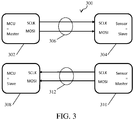
- Fig. 3 shows another illustrative embodiment of a sensing system 300.
- the SPI comprises a clock (SCLK) line and a master-output-slave-input (MOSI) line.
- SCLK clock
- MOSI master-output-slave-input
- the other lines of the SPI may also be omitted.
- data may be transmitted through these lines in two directions, but not simultaneously. Specifically, data may be transmitted in a first direction 306 (i.e., from microcontroller 302 to sensor module 304), and in a second direction 312 (i.e., from sensor module 310 to microcontroller 308).
- microcontroller 302 When data is transmitted in the first direction 306, microcontroller 302 acts as a master device, while sensor module 304 acts as a slave device. When data is transmitted is transmitted in the second direction 312, microcontroller 306 acts as a slave device, while sensor module 310 acts as a master device.
- the microcontroller and sensor module may switch roles, so as to enable using only the MOSI line for transmitting data in both directions. Switching roles may be implemented as follows.
- the processing unit i.e., microcontroller
- the sensor module are configured to operate in a slave mode by default.
- each of the processing unit and the sensor module may be configured to switch to a master mode of operation. It is noted that the processing unit is not necessarily a microcontroller; other processing units may also be used.
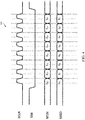
- Fig. 4 shows a timing diagram 400 of a serial peripheral interface.
- the timing requires a slave device to have a slave select signal SS_N pulled low so as to support slave mode.
- the communication master may calculate the duration it must stay in master mode based on the amount of data to be communicated.
- the duration of the master mode depends on an amount of data to be transmitted.
- the processing unit or the sensor module - as the case may be - does not remain in the master mode longer than necessary.
- the processing unit and the sensor module may be configured to switch back to the slave mode, thereby allowing another device to enter into the master mode.
- both devices may operate in a slave mode.
- the clock line connections of both devices are in input-mode (tri-state).
- the SCLK line is only utilized when communication takes place. For that reason, the SCLK line may be used to communicate an interrupt request from one device to the other device when no communication takes place.
- each of the sensor module and the processing unit is configured to transmit an interrupt request on the clock line when no communication takes place.
- the dedicated interrupt request (IRQ) line shown in Fig. 1 may also be omitted.
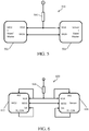
- Fig. 5 shows a further illustrative embodiment of a sensing system 500.
- the sensing system 500 comprises a microcontroller 502 and sensor module 504 that are communicatively coupled to each other via a clock (SCLK) line and a master-output-slave-input (MOSI) line. Both the microcontroller 502 and the sensor module 504 are configured to operate in a master mode and in a slave mode. The microcontroller 502 and the sensor module 504 are in the slave mode by default.
- SCLK clock
- MOSI master-output-slave-input
- both devices i.e., the microcontroller 502 and the sensor module 504 may be configured in slave mode, with each device providing an active low signal generated by its general-purpose input output pin SS_CON to its slave select input ⁇ SS, which means that both terminals of the clock line SCLK are in input-mode (tri-state).
- the communication between the microcontroller 502 and the sensor module 504 may take place in the following way.
- the requesting device may, while in slave mode, pull the SCLK line to clock-active-level which by default may be pulled up by a resistor 506 to clock-inactive-level. Pulling the SCLK line to clock-active-level may indicate an interrupt request to the receiving device.
- the device that receives such an interrupt request may wake up and may prepare for receiving data.
- the interrupt requesting device may calculate the expected data transmission duration based on the number of bytes to be transmitted, switch into master by de-asserting the slave select from its own SPI block, while it may be assured that the interrupt requesting device stays sufficiently long in master mode for assuring proper SPI communication.
- the loop from the general-purpose input output pin SS_CON to the slave select input ⁇ SS indicates that the existing interface signals of the existing SPI block are stimulated by an additional SS_CON to control the standard slave_select signal.
- the interrupt requesting device may transmit its message to the receiving device.
- the message may comprise an indication of how much information is sent.
- the transmitting device may re-activate the slave select signal and may thus switch back to the slave mode.
- Fig. 6 shows a further illustrative embodiment of a sensing system 600.
- the sensing system 600 comprises a microcontroller 602 and sensor module 604 that are communicatively coupled to each other via a clock (SCLK) line and a master-output-slave-input (MOSI) line. Both the microcontroller 602 and the sensor module 604 are configured to operate in a master mode and in a slave mode. The microcontroller 602 and the sensor module 604 are in the slave mode by default. The communication between the microcontroller 602 and the sensor module 604 may take place as described with reference to Fig. 5 .
- SCLK clock
- MOSI master-output-slave-input
- This example shows how the SCLK is used to transmit an interrupt request IRQ to the microcontroller 602 or the sensor module 604, as the case may be. Furthermore, it shows how the microcontroller 602 or the sensor module 604 asserts a slave select to its own SPI block (shown as an arrow from SS_CON to ⁇ SS).
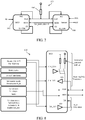
- Fig. 7 shows a further illustrative embodiment of a sensing system 700.
- the microcontroller 602 is configured to transmit a reset instruction to the sensor module 604.
- resetting the sensor module 604 may be simplified.
- a hardware reset may be replaced by a soft reset instruction communicated to the sensor module 604 by the microcontroller 602.
- the sensor module's SPI may have to be reset reliably by an external Power-On-Reset (POR) function to be able to receive the soft reset instruction under all conditions.
- POR Power-On-Reset
- Fig. 8 shows an illustrative embodiment of flow control 800.
- an example implementation is shown of the total flow control of a microcontroller of the kind set forth.
- the pull-up of the SCLK line to clock-inactive-level may be made configurable so as to enable power saving during communication.
- both devices may be configured to switch off IRQ-sensing while in master mode to avoid unstable behavior.
- each of the sensor module and the processing unit is configured to disregard interrupt requests when operating in the master mode. Thereby, unstable behavior of the sensing system may be avoided.
- Fig. 9 shows an illustrative embodiment of a communication method 900.
- the sensor module is configured to operate in the master mode during multiple data transmission cycles. In this way, delays caused by switching time overhead may be avoided.
- the duration of the master mode may again be derived from the expected number of data bytes to be sent to the receiving device.
- the sensor module may transmit an interrupt request to the microcontroller so that the microcontroller may wake up and receive new data.
- Operating in the master mode during multiple transmission cycles may be advantageous if the sensor module provides data in packets of a fixed number of bytes (e.g., 16 bytes). In that case, each data transmission cycle may include the transmission of said fixed number of bytes.
- the microcontroller requests the sensor module to perform a certain operation, for example to transmit data resulting from a fingerprint sensing operation. Subsequently, the sensor module performs this operation.
- both the microcontroller and the sensor module operate in the slave mode.
- the SCLK line may by default be pulled up by a resistor to clock-inactive-level.
- the sensor module may be in a predefined sleep mode.
- the senor module may wake up in response to the SCLK being pulled low, and the microcontroller may wait n cycles for the sensor module to wake up.
- the microcontroller sends x instruction bytes.
- the process of y cycles may end, and the microcontroller may pull the SCLK line high again (i.e., to clock-inactive-level) and switch back to the slave mode.
- the microcontroller may enter into a sleep mode.
- the microcontroller may wake up in response to the SCLK being pulled low, and the sensor module may wait n cycles for the microcontroller to wake up.
- the sensor module sends x response bytes. Subsequently, the process of y cycles may end, and the sensor module may pull the SCLK line high again (i.e., to clock-inactive-level) and switch back to the slave mode. Optionally, the sensor module may enter into a sleep mode.
- both the microcontroller and the sensor module operate in the slave mode again.
- the microcontroller may be made master of the flow control by giving it control over the start of a communication, while the sensor module is always configured to provide a response to a received instruction without having the option to stop sending responses. Furthermore, in an embodiment, the microcontroller may calculate a time interval using information contained in the instruction message. Within said time interval the microcontroller may expect a response from the sensor module. If no response is received within this time interval, the microcontroller may react by issuing a soft reset instruction to the sensor module, for example. It is furthermore noted that the presently disclosed system and method may support all SPI modes (i.e., modes 0, 1, 2 and 3).
- Fig. 10 shows an illustrative embodiment of a sensing system 1000.
- the sensing system 1000 comprises a microcontroller 1002 communicatively coupled to a fingerprint sensor 1004. Both the microcontroller 1002 and the fingerprint sensor 1004 are connected to a supply voltage 1006 and to ground 1008.
- the microcontroller 1002 and the fingerprint sensor 1004 are configured to communicate with each other via a serial peripheral interface (SPI) in a half-duplex mode of communication, using only a SCLK line and a MOSI line.
- SPI serial peripheral interface
- the sensing system 1000 may in total require four interconnections: a SCLK line, a MOSI line, and two power lines (Vdd, Gnd).
- Vdd, Gnd power lines
- the presently disclosed system and method may at least partly be executed by a computer program or a plurality of computer programs, which may exist in a variety of forms both active and inactive in a single computer system or across multiple computer systems.
- they may exist as software program(s) comprised of program instructions in source code, object code, executable code or other formats for performing some of the steps.
- Any of the above may be embodied on a computer-readable medium, which may include storage devices and signals, in compressed or uncompressed form.
- processor or “processing unit” refers to a data processing circuit that may be a microprocessor, a co-processor, a microcontroller, a microcomputer, a central processing unit, a field programmable gate array (FPGA), a programmable logic circuit, and/or any circuit that manipulates signals (analog or digital) based on operational instructions that are stored in a memory.
- processor or “processing unit” refers to a data processing circuit that may be a microprocessor, a co-processor, a microcontroller, a microcomputer, a central processing unit, a field programmable gate array (FPGA), a programmable logic circuit, and/or any circuit that manipulates signals (analog or digital) based on operational instructions that are stored in a memory.
- FPGA field programmable gate array
Landscapes
- Engineering & Computer Science (AREA)
- Theoretical Computer Science (AREA)
- Physics & Mathematics (AREA)
- General Physics & Mathematics (AREA)
- Signal Processing (AREA)
- General Engineering & Computer Science (AREA)
- Microelectronics & Electronic Packaging (AREA)
- Computer Hardware Design (AREA)
- Computer Networks & Wireless Communication (AREA)
- Automation & Control Theory (AREA)
- Measurement Of The Respiration, Hearing Ability, Form, And Blood Characteristics Of Living Organisms (AREA)
- Image Input (AREA)
- Arrangements For Transmission Of Measured Signals (AREA)
Abstract
Description
- The present disclosure relates to a biometric sensing system. Furthermore, the present disclosure relates to a method of communicating between a sensor module and a processing unit in a biometric sensing system, and to a corresponding computer program. Today, electronic devices such as smart cards are widely used in society. For example, smart cards may be used as electronic identity (eID) cards and payment cards (e.g., bank cards). Although these cards are relatively secure due to their cryptographic capabilities, they are usually not equipped with a user interface suitable for entering user credentials, i.e. a so-called "authentication interface". As a consequence, most card users still enter their PIN code through personal computers and laptops, which increases the risk that their credentials are intercepted by malicious software such as Trojans and key-logger programs. Some smart cards have been equipped with embedded touch-based user interfaces or sensor modules. An example of such a sensor module is a fingerprint sensor. However, it may be challenging to implement a simple, high-bandwidth interface between such a sensor module and processing components of the card (e.g., a microcontroller). The same challenge may exist for touch-based interfaces that are embedded in other types of electronic devices, such as Internet-of-Things (IoT) devices and wearable devices.
- In accordance with a first aspect of the present disclosure, a biometric sensing system is provided, comprising a sensor module; a processing unit communicatively coupled to the sensor module; wherein the sensor module and the processing unit are configured to communicate with each other in a half-duplex mode of communication.
- In an embodiment, the sensor module and the processing unit are communicatively coupled to each other via a serial peripheral interface.
- In an embodiment, the serial peripheral interface comprises a clock line and a master-output-slave-input line.
- In an embodiment, the sensor module and the processing unit are configured to operate in a slave mode by default.
- In an embodiment, each of the sensor module and the processing unit is configured to switch to a master mode of operation.
- In an embodiment, the duration of the master mode of operation depends on an amount of data to be transmitted.
- In an embodiment, each of the sensor module and the processing unit is configured to switch back to the slave mode.
- In an embodiment, each of the sensor module and the processing unit is configured to disregard interrupt requests when operating in the master mode.
- In an embodiment, the sensor module is configured to operate in the master mode during multiple data transmission cycles.
- In an embodiment, each of the sensor module and the processing unit is configured to transmit an interrupt request on a clock line when no communication takes place.
- In an embodiment, the processing unit is configured to transmit a reset instruction to the sensor module.
- In an embodiment, the processing unit is configured to control the start of a communication.
- In an embodiment, a smart card comprises a system of the kind set forth.
- In accordance with a second aspect of the present disclosure, a method of communicating between a sensor module and a processing unit in a biometric sensing system is conceived, wherein the sensor module and the processing unit communicate with each other in a half-duplex mode of communication.
- In accordance with a third aspect of the present disclosure, a computer program is provided, comprising non-transient executable instructions that, when executed by a sensor module or a processing unit, cause said sensor module and processing unit to carry out a method of the kind set forth.
- Embodiments will be described in more detail with reference to the appended drawings, in which:
-
Fig. 1 shows an example of a sensing system; -
Fig. 2 shows an illustrative embodiment of a sensing system; -
Fig. 3 shows another illustrative embodiment of a sensing system; -
Fig. 4 shows a timing diagram of a serial peripheral interface; -
Fig. 5 shows a further illustrative embodiment of a sensing system; -
Fig. 6 shows a further illustrative embodiment of a sensing system; -
Fig. 7 shows a further illustrative embodiment of a sensing system; -
Fig. 8 shows an illustrative embodiment of flow control; -
Fig. 9 shows an illustrative embodiment of a communication method; -
Fig. 10 shows a further illustrative embodiment of a sensing system. -
Fig. 1 shows an example of asensing system 100. Thesensing system 100 comprises amicrocontroller 102 that acts as a master device. Themicrocontroller 102 is an example of a processing unit of the kind set forth. Furthermore, thesensing system 100 comprises asensor module 104, e.g. a fingerprint sensor, which acts a slave device. Furthermore, both themicrocontroller 102 and thesensor module 104 are connected to asupply voltage 106 and toground 108. Themicrocontroller 102 and thesensor module 104 are configured to communicate with each other via a serial peripheral interface (SPI). An SPI often comprises at least six communication lines: a serial clock (SCLK) line, a master-output-slave-input (MOSI) line, a master-input-slave-output (MISO) line, a slave select (SS_N) line, an interrupt request (IRQ) line, and a reset (RST) line. A SPI is relatively fast, for example compared to an I2C interface, and it provides full-duplex communication. However, as shown inFig. 1 , a relatively large amount of communication lines or wires is required. It may be difficult to implement such a large amount of wires in some devices. For example, low-cost manufacturing of smart cards utilizes wire-embedding technology to create interconnections between embedded components. Since wire-embedding is a serial manufacturing process the number of interconnections between embedded components has a major impact on the throughput time during the wire-embedding manufacturing step. For that reason, it is desirable to reduce the number of interconnections between the components of a smart card. - Therefore, in accordance with a first aspect of the present disclosure, a biometric sensing system is provided, comprising a sensor module and a processing unit communicatively coupled to the sensor module. Furthermore, the sensor module and the processing unit are configured to communicate with each other in a half-duplex mode of communication. In this way, less communication lines are required between the sensor module and the processing unit. Furthermore, in an embodiment, the sensor module and the processing unit are communicatively coupled to each other via a serial peripheral interface (SPI). In this way, the communication between the sensor module and the processing unit may still be performed at an acceptable speed.
- More specifically, if one device is a sensor module that provides bulk data (e.g., fingerprint image data) to a processing unit, then a high bandwidth will be required for sending data from the sensor module to the processing unit, while a low bandwidth will be required for the transmission of data in the other direction. That is to say, the processing unit merely needs to transmit setup- and control-information to the sensor module. The SPI has been developed to provide high bandwidth in both directions, providing full-duplex communication. In a sensing system of the kind set forth, it may be sufficient to provide a high bandwidth only in one direction, i.e. from the sensor module to the processing unit. Thus, the sensor module and the processing unit may communicate with each other in a half-duplex mode of communication. The biometric sensing system may be used to advantage in a smart card, or in any other device in which creating sufficient communication lines presents a challenge (e.g., IoT devices or wearable devices). The biometric sensing system may be a fingerprint sensing system. It is noted that the sensing system may also be another type of biometric sensing system. For instance, the presently disclosed system and method may be used to advantage in high-bandwidth streaming devices equipped with a face recognition camera, an iris scan camera or a vein pattern camera.
-
Fig. 2 shows an illustrative embodiment of asensing system 200. Thesensing system 200 comprises amicrocontroller 202 communicatively coupled to asensor module 204. Both themicrocontroller 202 and thesensor module 204 are connected to asupply voltage 106 and toground 108. Themicrocontroller 202 and thesensor module 204 are configured to communicate with each other via a serial peripheral interface (SPI). However, in accordance with the present disclosure, themicrocontroller 202 and thesensor module 204 are configured to communicate with each other in a half-duplex mode of communication. Therefore, the MISO line of the SPI may be omitted. -
Fig. 3 shows another illustrative embodiment of asensing system 300. In this embodiment, the SPI comprises a clock (SCLK) line and a master-output-slave-input (MOSI) line. As will be explained with reference to the various embodiments herein, the other lines of the SPI may also be omitted. In accordance with the principles of half-duplex communication, data may be transmitted through these lines in two directions, but not simultaneously. Specifically, data may be transmitted in a first direction 306 (i.e., frommicrocontroller 302 to sensor module 304), and in a second direction 312 (i.e., fromsensor module 310 to microcontroller 308). When data is transmitted in thefirst direction 306,microcontroller 302 acts as a master device, whilesensor module 304 acts as a slave device. When data is transmitted is transmitted in thesecond direction 312,microcontroller 306 acts as a slave device, whilesensor module 310 acts as a master device. Thus, the microcontroller and sensor module may switch roles, so as to enable using only the MOSI line for transmitting data in both directions. Switching roles may be implemented as follows. In an embodiment, the processing unit (i.e., microcontroller) and the sensor module are configured to operate in a slave mode by default. Furthermore, each of the processing unit and the sensor module may be configured to switch to a master mode of operation. It is noted that the processing unit is not necessarily a microcontroller; other processing units may also be used. -
Fig. 4 shows a timing diagram 400 of a serial peripheral interface. In particular, the timing requires a slave device to have a slave select signal SS_N pulled low so as to support slave mode. The communication master may calculate the duration it must stay in master mode based on the amount of data to be communicated. Thus, in an embodiment, the duration of the master mode depends on an amount of data to be transmitted. Thereby, the processing unit or the sensor module - as the case may be - does not remain in the master mode longer than necessary. Furthermore, the processing unit and the sensor module may be configured to switch back to the slave mode, thereby allowing another device to enter into the master mode. - As mentioned above, by default both devices may operate in a slave mode. In this mode, the clock line connections of both devices are in input-mode (tri-state). As shown in
Fig. 4 the clock (SCLK) line is only utilized when communication takes place. For that reason, the SCLK line may be used to communicate an interrupt request from one device to the other device when no communication takes place. Thus, in an embodiment, each of the sensor module and the processing unit is configured to transmit an interrupt request on the clock line when no communication takes place. In this way, the dedicated interrupt request (IRQ) line shown inFig. 1 may also be omitted. -
Fig. 5 shows a further illustrative embodiment of asensing system 500. Thesensing system 500 comprises amicrocontroller 502 andsensor module 504 that are communicatively coupled to each other via a clock (SCLK) line and a master-output-slave-input (MOSI) line. Both themicrocontroller 502 and thesensor module 504 are configured to operate in a master mode and in a slave mode. Themicrocontroller 502 and thesensor module 504 are in the slave mode by default. More specifically, in a default mode both devices (i.e., themicrocontroller 502 and the sensor module 504) may be configured in slave mode, with each device providing an active low signal generated by its general-purpose input output pin SS_CON to its slave select input \SS, which means that both terminals of the clock line SCLK are in input-mode (tri-state). The communication between themicrocontroller 502 and thesensor module 504 may take place in the following way. In a first step the requesting device may, while in slave mode, pull the SCLK line to clock-active-level which by default may be pulled up by aresistor 506 to clock-inactive-level. Pulling the SCLK line to clock-active-level may indicate an interrupt request to the receiving device. In a second step the device that receives such an interrupt request may wake up and may prepare for receiving data. In a third step the interrupt requesting device may calculate the expected data transmission duration based on the number of bytes to be transmitted, switch into master by de-asserting the slave select from its own SPI block, while it may be assured that the interrupt requesting device stays sufficiently long in master mode for assuring proper SPI communication. The loop from the general-purpose input output pin SS_CON to the slave select input \SS indicates that the existing interface signals of the existing SPI block are stimulated by an additional SS_CON to control the standard slave_select signal. In a fourth step the interrupt requesting device may transmit its message to the receiving device. The message may comprise an indication of how much information is sent. In a fifth step the transmitting device may re-activate the slave select signal and may thus switch back to the slave mode. -
Fig. 6 shows a further illustrative embodiment of asensing system 600. Thesensing system 600 comprises amicrocontroller 602 andsensor module 604 that are communicatively coupled to each other via a clock (SCLK) line and a master-output-slave-input (MOSI) line. Both themicrocontroller 602 and thesensor module 604 are configured to operate in a master mode and in a slave mode. Themicrocontroller 602 and thesensor module 604 are in the slave mode by default. The communication between themicrocontroller 602 and thesensor module 604 may take place as described with reference toFig. 5 . This example shows how the SCLK is used to transmit an interrupt request IRQ to themicrocontroller 602 or thesensor module 604, as the case may be. Furthermore, it shows how themicrocontroller 602 or thesensor module 604 asserts a slave select to its own SPI block (shown as an arrow from SS_CON to \SS). -
Fig. 7 shows a further illustrative embodiment of asensing system 700. In this embodiment, themicrocontroller 602 is configured to transmit a reset instruction to thesensor module 604. Thereby, resetting thesensor module 604 may be simplified. In particular, for resetting thesensor module 604, a hardware reset may be replaced by a soft reset instruction communicated to thesensor module 604 by themicrocontroller 602. In order to achieve this, the sensor module's SPI may have to be reset reliably by an external Power-On-Reset (POR) function to be able to receive the soft reset instruction under all conditions. -
Fig. 8 shows an illustrative embodiment offlow control 800. In particular, an example implementation is shown of the total flow control of a microcontroller of the kind set forth. As shown, the pull-up of the SCLK line to clock-inactive-level may be made configurable so as to enable power saving during communication. Furthermore, both devices may be configured to switch off IRQ-sensing while in master mode to avoid unstable behavior. In other words, in an embodiment, each of the sensor module and the processing unit is configured to disregard interrupt requests when operating in the master mode. Thereby, unstable behavior of the sensing system may be avoided. -
Fig. 9 shows an illustrative embodiment of acommunication method 900. As mentioned above, in an embodiment, the sensor module is configured to operate in the master mode during multiple data transmission cycles. In this way, delays caused by switching time overhead may be avoided. The duration of the master mode may again be derived from the expected number of data bytes to be sent to the receiving device. The sensor module may transmit an interrupt request to the microcontroller so that the microcontroller may wake up and receive new data. Operating in the master mode during multiple transmission cycles may be advantageous if the sensor module provides data in packets of a fixed number of bytes (e.g., 16 bytes). In that case, each data transmission cycle may include the transmission of said fixed number of bytes. In the example shown inFig. 9 , the microcontroller requests the sensor module to perform a certain operation, for example to transmit data resulting from a fingerprint sensing operation. Subsequently, the sensor module performs this operation. - In a
first step 902, both the microcontroller and the sensor module operate in the slave mode. For example, as mentioned above, the SCLK line may by default be pulled up by a resistor to clock-inactive-level. Optionally, the sensor module may be in a predefined sleep mode. - In a
second step 904, the microcontroller may be switched by a computer program to the master mode. More specifically, a process comprising y cycles may be started. If y=1, and an instruction is ready, the microcontroller pulls the SCLK line low (i.e., to clock-active-level) with its own SCLK detection disabled. Furthermore, the microcontroller is set as master for a duration of x*y bytes. If y>1, and the instruction is ready, the microcontroller pulls the SCLK line low (i.e., to clock-active-level) with its own SCLK detection disabled. Optionally, if the sensor module is in the sleep-mode, it may wake up in response to the SCLK being pulled low, and the microcontroller may wait n cycles for the sensor module to wake up. Next, the microcontroller sends x instruction bytes. Subsequently, the process of y cycles may end, and the microcontroller may pull the SCLK line high again (i.e., to clock-inactive-level) and switch back to the slave mode. Optionally, the microcontroller may enter into a sleep mode. - In a
third step 906, the sensor module may switch to the master mode. More specifically, a process comprising y cycles may be started. If y=1 and a response is ready, the sensor module pulls the SCLK line low (i.e., to clock-active-level) with its own SCLK detection disabled. Furthermore, the sensor module is set as master for a duration of x*y bytes. If y>1, and the response is ready, the sensor module pulls the SCLK line low (i.e., to clock-active-level) with its own SCLK detection disabled. Optionally, if the microcontroller is in the sleep-mode, it may wake up in response to the SCLK being pulled low, and the sensor module may wait n cycles for the microcontroller to wake up. Next, the sensor module sends x response bytes. Subsequently, the process of y cycles may end, and the sensor module may pull the SCLK line high again (i.e., to clock-inactive-level) and switch back to the slave mode. Optionally, the sensor module may enter into a sleep mode. - In a
fourth step 908, both the microcontroller and the sensor module operate in the slave mode again. - In an embodiment, the microcontroller may be made master of the flow control by giving it control over the start of a communication, while the sensor module is always configured to provide a response to a received instruction without having the option to stop sending responses. Furthermore, in an embodiment, the microcontroller may calculate a time interval using information contained in the instruction message. Within said time interval the microcontroller may expect a response from the sensor module. If no response is received within this time interval, the microcontroller may react by issuing a soft reset instruction to the sensor module, for example. It is furthermore noted that the presently disclosed system and method may support all SPI modes (i.e.,
modes 0, 1, 2 and 3). -
Fig. 10 shows an illustrative embodiment of asensing system 1000. Thesensing system 1000 comprises amicrocontroller 1002 communicatively coupled to afingerprint sensor 1004. Both themicrocontroller 1002 and thefingerprint sensor 1004 are connected to asupply voltage 1006 and toground 1008. In accordance with the present disclosure, themicrocontroller 1002 and thefingerprint sensor 1004 are configured to communicate with each other via a serial peripheral interface (SPI) in a half-duplex mode of communication, using only a SCLK line and a MOSI line. Thus, thesensing system 1000 may in total require four interconnections: a SCLK line, a MOSI line, and two power lines (Vdd, Gnd). Thus, the number of interconnections between the microcontroller and the fingerprint sensor is significantly reduced. - The presently disclosed system and method may at least partly be executed by a computer program or a plurality of computer programs, which may exist in a variety of forms both active and inactive in a single computer system or across multiple computer systems. For example, they may exist as software program(s) comprised of program instructions in source code, object code, executable code or other formats for performing some of the steps. Any of the above may be embodied on a computer-readable medium, which may include storage devices and signals, in compressed or uncompressed form. The term "processor" or "processing unit" refers to a data processing circuit that may be a microprocessor, a co-processor, a microcontroller, a microcomputer, a central processing unit, a field programmable gate array (FPGA), a programmable logic circuit, and/or any circuit that manipulates signals (analog or digital) based on operational instructions that are stored in a memory.
- It is noted that the embodiments above have been described with reference to different subject-matters. In particular, some embodiments may have been described with reference to method-type claims whereas other embodiments may have been described with reference to apparatus-type claims. However, a person skilled in the art will gather from the above that, unless otherwise indicated, in addition to any combination of features belonging to one type of subject-matter also any combination of features relating to different subject-matters, in particular a combination of features of the method-type claims and features of the apparatus-type claims, is considered to be disclosed with this document.
- Furthermore, it is noted that the drawings are schematic. In different drawings, similar or identical elements are provided with the same reference signs. Furthermore, it is noted that in an effort to provide a concise description of the illustrative embodiments, implementation details which fall into the customary practice of the skilled person may not have been described. It should be appreciated that in the development of any such implementation, as in any engineering or design project, numerous implementation-specific decisions must be made in order to achieve the developers' specific goals, such as compliance with system-related and business-related constraints, which may vary from one implementation to another. Moreover, it should be appreciated that such a development effort might be complex and time consuming, but would nevertheless be a routine undertaking of design, fabrication, and manufacture for those of ordinary skill.
- Finally, it is noted that the skilled person will be able to design many alternative embodiments without departing from the scope of the appended claims. In the claims, any reference sign placed between parentheses shall not be construed as limiting the claim. The word "comprise(s)" or "comprising" does not exclude the presence of elements or steps other than those listed in a claim. The word "a" or "an" preceding an element does not exclude the presence of a plurality of such elements. Measures recited in the claims may be implemented by means of hardware comprising several distinct elements and/or by means of a suitably programmed processor. In a device claim enumerating several means, several of these means may be embodied by one and the same item of hardware. The mere fact that certain measures are recited in mutually different dependent claims does not indicate that a combination of these measures cannot be used to advantage.
-
- 100
- sensing system
- 102
- microcontroller
- 104
- sensor module
- 106
- supply voltage
- 108
- ground
- 200
- sensing system
- 202
- microcontroller
- 204
- sensor module
- 300
- sensing system
- 302
- microcontroller
- 304
- sensor module
- 306
- first direction
- 308
- microcontroller
- 310
- sensor module
- 312
- second direction
- 400
- timing diagram of an SPI
- 500
- sensing system
- 502
- microcontroller
- 504
- sensor module
- 506
- resistor
- 600
- sensing system
- 602
- microcontroller
- 604
- sensor module
- 606
- resistor
- 700
- sensing system
- 800
- flow control
- 900
- communication method
- 902
- first step
- 904
- second step
- 906
- third step
- 908
- fourth step
- 1000
- sensing system
- 1002
- microcontroller
- 1004
- fingerprint sensor
- 1006
- supply voltage
- 1008
- ground
- 1010
- interconnections
Claims (15)
- A biometric sensing system comprising:a sensor module;a processing unit communicatively coupled to the sensor module;wherein the sensor module and the processing unit are configured to communicate with each other in a half-duplex mode of communication.
- The system of claim 1, wherein the sensor module and the processing unit are communicatively coupled to each other via a serial peripheral interface.
- The system of claim 2, wherein the serial peripheral interface comprises a clock line and a master-output-slave-input line.
- The system of any preceding claim, wherein the sensor module and the processing unit are configured to operate in a slave mode by default.
- The system of claim 4, wherein each of the sensor module and the processing unit is configured to switch to a master mode of operation.
- The system of claim 5, wherein the duration of the master mode of operation depends on an amount of data to be transmitted.
- The system of claim 5 or 6, wherein each of the sensor module and the processing unit is configured to switch back to the slave mode.
- The system of any one of claims 5 to 7, wherein each of the sensor module and the processing unit is configured to disregard interrupt requests when operating in the master mode.
- The system of any one of claims 5 to 8, wherein the sensor module is configured to operate in the master mode during multiple data transmission cycles.
- The system of any preceding claim, wherein each of the sensor module and the processing unit is configured to transmit an interrupt request on a clock line when no communication takes place.
- The system of any preceding claim, wherein the processing unit is configured to transmit a reset instruction to the sensor module.
- The system of any preceding claim, wherein the processing unit is configured to control the start of a communication.
- A smart card comprising the system of any preceding claim.
- A method of communicating between a sensor module and a processing unit in a biometric sensing system, wherein the sensor module and the processing unit communicate with each other in a half-duplex mode of communication.
- A computer program comprising non-transient executable instructions that, when executed by a sensor module or a processing unit, cause said sensor module and processing unit to carry out the method of claim 14.
Priority Applications (3)
| Application Number | Priority Date | Filing Date | Title |
|---|---|---|---|
| EP17181138.3A EP3428804A1 (en) | 2017-07-13 | 2017-07-13 | Biometric sensing system |
| CN201810766661.3A CN109255419B (en) | 2017-07-13 | 2018-07-12 | Biometric sensor systems |
| US16/034,352 US10659213B2 (en) | 2017-07-13 | 2018-07-13 | Biometric sensing system |
Applications Claiming Priority (1)
| Application Number | Priority Date | Filing Date | Title |
|---|---|---|---|
| EP17181138.3A EP3428804A1 (en) | 2017-07-13 | 2017-07-13 | Biometric sensing system |
Publications (1)
| Publication Number | Publication Date |
|---|---|
| EP3428804A1 true EP3428804A1 (en) | 2019-01-16 |
Family
ID=59350705
Family Applications (1)
| Application Number | Title | Priority Date | Filing Date |
|---|---|---|---|
| EP17181138.3A Ceased EP3428804A1 (en) | 2017-07-13 | 2017-07-13 | Biometric sensing system |
Country Status (3)
| Country | Link |
|---|---|
| US (1) | US10659213B2 (en) |
| EP (1) | EP3428804A1 (en) |
| CN (1) | CN109255419B (en) |
Cited By (1)
| Publication number | Priority date | Publication date | Assignee | Title |
|---|---|---|---|---|
| CN114402367A (en) * | 2020-07-29 | 2022-04-26 | 指纹卡安娜卡敦知识产权有限公司 | Adaptive readout from optical biometric sensor to host device |
Families Citing this family (2)
| Publication number | Priority date | Publication date | Assignee | Title |
|---|---|---|---|---|
| KR102599277B1 (en) * | 2018-12-13 | 2023-11-07 | 엘지디스플레이 주식회사 | Touch sensor display device and interfacing method thereof |
| TWI812194B (en) * | 2022-04-27 | 2023-08-11 | 凌通科技股份有限公司 | Serial peripheral interface compatibility extension switching method and embedded system using the same |
Citations (3)
| Publication number | Priority date | Publication date | Assignee | Title |
|---|---|---|---|---|
| US20090228714A1 (en) * | 2004-11-18 | 2009-09-10 | Biogy, Inc. | Secure mobile device with online vault |
| US20110122978A1 (en) * | 2008-05-30 | 2011-05-26 | Continental Teves Ag & Co, Ohg | Serial peripheral interface having a reduced number of connecting lines |
| US20170104733A1 (en) * | 2015-10-09 | 2017-04-13 | Intel Corporation | Device, system and method for low speed communication of sensor information |
Family Cites Families (8)
| Publication number | Priority date | Publication date | Assignee | Title |
|---|---|---|---|---|
| JPH05334239A (en) * | 1992-06-03 | 1993-12-17 | Matsushita Electric Ind Co Ltd | Bus system |
| JP4424572B2 (en) * | 2000-09-19 | 2010-03-03 | 本田技研工業株式会社 | Communication device with group registration function |
| WO2006105094A2 (en) * | 2005-03-29 | 2006-10-05 | Duke University | Sensor system for identifying and tracking movements of multiple sources |
| US9904637B2 (en) * | 2014-11-26 | 2018-02-27 | Qualcomm Incorporated | In-band interrupt time stamp |
| US10037528B2 (en) * | 2015-01-14 | 2018-07-31 | Tactilis Sdn Bhd | Biometric device utilizing finger sequence for authentication |
| US10002091B2 (en) * | 2015-03-26 | 2018-06-19 | Honeywell International Inc. | Master/slave management for redundant process controller modules |
| EP3091459B1 (en) * | 2015-05-07 | 2020-06-24 | Sorin CRM SAS | Systems and methods for wireless communication with implantable and body-worn devices |
| GB201602371D0 (en) * | 2016-02-10 | 2016-03-23 | Zwipe As | Smartcard and method for controlling a smartcard |
-
2017
- 2017-07-13 EP EP17181138.3A patent/EP3428804A1/en not_active Ceased
-
2018
- 2018-07-12 CN CN201810766661.3A patent/CN109255419B/en active Active
- 2018-07-13 US US16/034,352 patent/US10659213B2/en active Active
Patent Citations (3)
| Publication number | Priority date | Publication date | Assignee | Title |
|---|---|---|---|---|
| US20090228714A1 (en) * | 2004-11-18 | 2009-09-10 | Biogy, Inc. | Secure mobile device with online vault |
| US20110122978A1 (en) * | 2008-05-30 | 2011-05-26 | Continental Teves Ag & Co, Ohg | Serial peripheral interface having a reduced number of connecting lines |
| US20170104733A1 (en) * | 2015-10-09 | 2017-04-13 | Intel Corporation | Device, system and method for low speed communication of sensor information |
Non-Patent Citations (7)
| Title |
|---|
| AMIT SRIVASTAVA: "SPECIFICATION FOR I3C - IMPROVED INTER-INTEGRATED CIRCUIT - VERSION 1.0 - public release edition", 23 December 2016 (2016-12-23), XP055504743, Retrieved from the Internet <URL:https://cdn2.hubspot.net/hubfs/2384176/public-specifications/mipi_I3C_specification_v1-0_public_edition.pdf?utm_campaign=I3C%20v1.0%20Download&utm_medium=email&_hsenc=p2ANqtz-9ktG3MvcF8KaQXcGuMpHFtJ_rtj45SfOVZmDilAKEpZwEl4CxQgERB1S0xsNU-NzB_p6uDw7HU5Ra0nqvkKEhOdwlGBo9K5MpsZEubX39ah348GbI&_hsmi=2&utm> [retrieved on 20180905] * |
| ANONYMOUS: "I2C - Wikipedia", 16 June 2017 (2017-06-16), XP055405425, Retrieved from the Internet <URL:https://en.wikipedia.org/w/index.php?title=I2C&oldid=785951469> [retrieved on 20170911] * |
| ANONYMOUS: "Serial Peripheral Interface Bus - Wikipedia", 10 July 2017 (2017-07-10), XP055405537, Retrieved from the Internet <URL:https://en.wikipedia.org/w/index.php?title=Serial_Peripheral_Interface_Bus&oldid=789967215> [retrieved on 20170911] * |
| CADENCE DESIGN SYSTEMS: "Whiteboard Wednesdays - Advantages of the MIPI I3C Interface", YOU TUBE, 1 June 2016 (2016-06-01), pages 1, XP054977723, Retrieved from the Internet <URL:https://www.youtube.com/watch?v=K8LjIEC3UEo> [retrieved on 20170911] * |
| MIPI ALLIANCE: "Introduction to the MIPI I3C Standardized Sensor Interface", 1 August 2016 (2016-08-01), XP055405430, Retrieved from the Internet <URL:https://cdn2.hubspot.net/hubfs/2384176/MIPI_Alliance_I3C_Whitepaper.pdf> [retrieved on 20170911] * |
| MIPI DEVCON 2016 - A DEVELOPER'S GUIDE TO MIPI I3C IMPLEMENTATION: "MIPI DevCon 2016 - A Developer's Guide to MIPI I3C Implementation", 17 February 2017 (2017-02-17), XP054977721, Retrieved from the Internet <URL:https://www.youtube.com/watch?v=cL1rhfqHj88> [retrieved on 20170911] * |
| MOTOROLA: "SPI Block Guide V04.01", 14 July 2004 (2004-07-14), XP055733482, Retrieved from the Internet <URL:https://www.nxp.com/files-static/microcontrollers/doc/ref_manual/S12SPIV4.pdf> [retrieved on 20200923] * |
Cited By (2)
| Publication number | Priority date | Publication date | Assignee | Title |
|---|---|---|---|---|
| CN114402367A (en) * | 2020-07-29 | 2022-04-26 | 指纹卡安娜卡敦知识产权有限公司 | Adaptive readout from optical biometric sensor to host device |
| EP3997579A4 (en) * | 2020-07-29 | 2022-10-05 | Fingerprint Cards Anacatum IP AB | ADAPTIVE READING FROM AN OPTICAL BIOMETRIC SENSOR TO A HOST DEVICE |
Also Published As
| Publication number | Publication date |
|---|---|
| CN109255419A (en) | 2019-01-22 |
| US10659213B2 (en) | 2020-05-19 |
| CN109255419B (en) | 2024-07-09 |
| US20190020462A1 (en) | 2019-01-17 |
Similar Documents
| Publication | Publication Date | Title |
|---|---|---|
| US10140242B2 (en) | General purpose input/output (GPIO) signal bridging with I3C bus interfaces and virtualization in a multi-node network | |
| US10482058B2 (en) | Biometric sensing system and communication method | |
| KR101665985B1 (en) | Virtual gpio | |
| US9298210B2 (en) | Clock gating circuit and bus system | |
| EP2587385A1 (en) | Usb key device and method for realizing intelligent card communication using usb interface | |
| US10659213B2 (en) | Biometric sensing system | |
| CN100468378C (en) | SPI device communication circuit | |
| CN110764585B (en) | A Universal Independent BMC Board | |
| US10732669B2 (en) | Serial peripheral interface and methods of operating same | |
| CN102770851B (en) | Restoring stability on unstable buses | |
| US20160062426A1 (en) | Chip Device and Electronic System thereof | |
| US11907155B2 (en) | Bus system connecting slave devices with single-wire data access communication | |
| US7457904B2 (en) | Methods and systems for a reference clock | |
| US6874047B1 (en) | System and method for implementing an SMBus/I2C interface on a network interface card | |
| TWI245179B (en) | Method for PCI express power management using a PCI PM mechanism in a computer system | |
| US7340554B2 (en) | USB host controller with DMA capability | |
| CN113282532B (en) | Communication device, communication method of communication device and electronic equipment | |
| TWI237764B (en) | Control chip with function for inhibiting bus cycle, circuit and method thereof | |
| US20070156934A1 (en) | High-speed PCI Interface System and A Reset Method Thereof | |
| EP1627312B1 (en) | Usb host controller with dma capability | |
| CN102855204B (en) | A kind of access control method and system and master control borad | |
| CN117370245A (en) | Rate adaptation system and USB3 speed reduction bridge suitable for USB3 speed reduction bridge | |
| US20220100245A1 (en) | Enablement of Wake on Finger Print Sensor without USB Enumeration | |
| JP2799753B2 (en) | Pulse width modulation controller | |
| CN101398794A (en) | Bus logic gateway circuit for multiple interrupt request signals |
Legal Events
| Date | Code | Title | Description |
|---|---|---|---|
| PUAI | Public reference made under article 153(3) epc to a published international application that has entered the european phase |
Free format text: ORIGINAL CODE: 0009012 |
|
| STAA | Information on the status of an ep patent application or granted ep patent |
Free format text: STATUS: THE APPLICATION HAS BEEN PUBLISHED |
|
| AK | Designated contracting states |
Kind code of ref document: A1 Designated state(s): AL AT BE BG CH CY CZ DE DK EE ES FI FR GB GR HR HU IE IS IT LI LT LU LV MC MK MT NL NO PL PT RO RS SE SI SK SM TR |
|
| AX | Request for extension of the european patent |
Extension state: BA ME |
|
| STAA | Information on the status of an ep patent application or granted ep patent |
Free format text: STATUS: REQUEST FOR EXAMINATION WAS MADE |
|
| 17P | Request for examination filed |
Effective date: 20190716 |
|
| RBV | Designated contracting states (corrected) |
Designated state(s): AL AT BE BG CH CY CZ DE DK EE ES FI FR GB GR HR HU IE IS IT LI LT LU LV MC MK MT NL NO PL PT RO RS SE SI SK SM TR |
|
| STAA | Information on the status of an ep patent application or granted ep patent |
Free format text: STATUS: EXAMINATION IS IN PROGRESS |
|
| 17Q | First examination report despatched |
Effective date: 20200929 |
|
| STAA | Information on the status of an ep patent application or granted ep patent |
Free format text: STATUS: THE APPLICATION HAS BEEN REFUSED |
|
| 18R | Application refused |
Effective date: 20240201 |