EP3425666A1 - Semiconductor module - Google Patents
Semiconductor module Download PDFInfo
- Publication number
- EP3425666A1 EP3425666A1 EP18180320.6A EP18180320A EP3425666A1 EP 3425666 A1 EP3425666 A1 EP 3425666A1 EP 18180320 A EP18180320 A EP 18180320A EP 3425666 A1 EP3425666 A1 EP 3425666A1
- Authority
- EP
- European Patent Office
- Prior art keywords
- electrode
- outer peripheral
- semiconductor substrate
- recessed portion
- solder layer
- Prior art date
- Legal status (The legal status is an assumption and is not a legal conclusion. Google has not performed a legal analysis and makes no representation as to the accuracy of the status listed.)
- Withdrawn
Links
Images


Classifications
-
- H—ELECTRICITY
- H10—SEMICONDUCTOR DEVICES; ELECTRIC SOLID-STATE DEVICES NOT OTHERWISE PROVIDED FOR
- H10W—GENERIC PACKAGES, INTERCONNECTIONS, CONNECTORS OR OTHER CONSTRUCTIONAL DETAILS OF DEVICES COVERED BY CLASS H10
- H10W70/00—Package substrates; Interposers; Redistribution layers [RDL]
- H10W70/60—Insulating or insulated package substrates; Interposers; Redistribution layers
-
- H—ELECTRICITY
- H10—SEMICONDUCTOR DEVICES; ELECTRIC SOLID-STATE DEVICES NOT OTHERWISE PROVIDED FOR
- H10W—GENERIC PACKAGES, INTERCONNECTIONS, CONNECTORS OR OTHER CONSTRUCTIONAL DETAILS OF DEVICES COVERED BY CLASS H10
- H10W72/00—Interconnections or connectors in packages
-
- H—ELECTRICITY
- H10—SEMICONDUCTOR DEVICES; ELECTRIC SOLID-STATE DEVICES NOT OTHERWISE PROVIDED FOR
- H10W—GENERIC PACKAGES, INTERCONNECTIONS, CONNECTORS OR OTHER CONSTRUCTIONAL DETAILS OF DEVICES COVERED BY CLASS H10
- H10W40/00—Arrangements for thermal protection or thermal control
- H10W40/20—Arrangements for cooling
- H10W40/25—Arrangements for cooling characterised by their materials
-
- H—ELECTRICITY
- H10—SEMICONDUCTOR DEVICES; ELECTRIC SOLID-STATE DEVICES NOT OTHERWISE PROVIDED FOR
- H10W—GENERIC PACKAGES, INTERCONNECTIONS, CONNECTORS OR OTHER CONSTRUCTIONAL DETAILS OF DEVICES COVERED BY CLASS H10
- H10W40/00—Arrangements for thermal protection or thermal control
- H10W40/20—Arrangements for cooling
- H10W40/25—Arrangements for cooling characterised by their materials
- H10W40/255—Arrangements for cooling characterised by their materials having a laminate or multilayered structure, e.g. direct bond copper [DBC] ceramic substrates
-
- H—ELECTRICITY
- H10—SEMICONDUCTOR DEVICES; ELECTRIC SOLID-STATE DEVICES NOT OTHERWISE PROVIDED FOR
- H10W—GENERIC PACKAGES, INTERCONNECTIONS, CONNECTORS OR OTHER CONSTRUCTIONAL DETAILS OF DEVICES COVERED BY CLASS H10
- H10W70/00—Package substrates; Interposers; Redistribution layers [RDL]
- H10W70/20—Conductive package substrates serving as an interconnection, e.g. metal plates
-
- H—ELECTRICITY
- H10—SEMICONDUCTOR DEVICES; ELECTRIC SOLID-STATE DEVICES NOT OTHERWISE PROVIDED FOR
- H10W—GENERIC PACKAGES, INTERCONNECTIONS, CONNECTORS OR OTHER CONSTRUCTIONAL DETAILS OF DEVICES COVERED BY CLASS H10
- H10W70/00—Package substrates; Interposers; Redistribution layers [RDL]
- H10W70/40—Leadframes
-
- H—ELECTRICITY
- H10—SEMICONDUCTOR DEVICES; ELECTRIC SOLID-STATE DEVICES NOT OTHERWISE PROVIDED FOR
- H10W—GENERIC PACKAGES, INTERCONNECTIONS, CONNECTORS OR OTHER CONSTRUCTIONAL DETAILS OF DEVICES COVERED BY CLASS H10
- H10W70/00—Package substrates; Interposers; Redistribution layers [RDL]
- H10W70/40—Leadframes
- H10W70/411—Chip-supporting parts, e.g. die pads
- H10W70/417—Bonding materials between chips and die pads
-
- H—ELECTRICITY
- H10—SEMICONDUCTOR DEVICES; ELECTRIC SOLID-STATE DEVICES NOT OTHERWISE PROVIDED FOR
- H10W—GENERIC PACKAGES, INTERCONNECTIONS, CONNECTORS OR OTHER CONSTRUCTIONAL DETAILS OF DEVICES COVERED BY CLASS H10
- H10W70/00—Package substrates; Interposers; Redistribution layers [RDL]
- H10W70/40—Leadframes
- H10W70/421—Shapes or dispositions
- H10W70/424—Cross-sectional shapes
-
- H—ELECTRICITY
- H10—SEMICONDUCTOR DEVICES; ELECTRIC SOLID-STATE DEVICES NOT OTHERWISE PROVIDED FOR
- H10W—GENERIC PACKAGES, INTERCONNECTIONS, CONNECTORS OR OTHER CONSTRUCTIONAL DETAILS OF DEVICES COVERED BY CLASS H10
- H10W70/00—Package substrates; Interposers; Redistribution layers [RDL]
- H10W70/40—Leadframes
- H10W70/456—Materials
- H10W70/457—Materials of metallic layers on leadframes
-
- H—ELECTRICITY
- H10—SEMICONDUCTOR DEVICES; ELECTRIC SOLID-STATE DEVICES NOT OTHERWISE PROVIDED FOR
- H10W—GENERIC PACKAGES, INTERCONNECTIONS, CONNECTORS OR OTHER CONSTRUCTIONAL DETAILS OF DEVICES COVERED BY CLASS H10
- H10W70/00—Package substrates; Interposers; Redistribution layers [RDL]
- H10W70/40—Leadframes
- H10W70/461—Leadframes specially adapted for cooling
-
- H—ELECTRICITY
- H10—SEMICONDUCTOR DEVICES; ELECTRIC SOLID-STATE DEVICES NOT OTHERWISE PROVIDED FOR
- H10W—GENERIC PACKAGES, INTERCONNECTIONS, CONNECTORS OR OTHER CONSTRUCTIONAL DETAILS OF DEVICES COVERED BY CLASS H10
- H10W70/00—Package substrates; Interposers; Redistribution layers [RDL]
- H10W70/40—Leadframes
- H10W70/481—Leadframes for devices being provided for in groups H10D8/00 - H10D48/00
-
- H—ELECTRICITY
- H10—SEMICONDUCTOR DEVICES; ELECTRIC SOLID-STATE DEVICES NOT OTHERWISE PROVIDED FOR
- H10W—GENERIC PACKAGES, INTERCONNECTIONS, CONNECTORS OR OTHER CONSTRUCTIONAL DETAILS OF DEVICES COVERED BY CLASS H10
- H10W70/00—Package substrates; Interposers; Redistribution layers [RDL]
- H10W70/60—Insulating or insulated package substrates; Interposers; Redistribution layers
- H10W70/62—Insulating or insulated package substrates; Interposers; Redistribution layers characterised by their interconnections
- H10W70/65—Shapes or dispositions of interconnections
-
- H—ELECTRICITY
- H10—SEMICONDUCTOR DEVICES; ELECTRIC SOLID-STATE DEVICES NOT OTHERWISE PROVIDED FOR
- H10W—GENERIC PACKAGES, INTERCONNECTIONS, CONNECTORS OR OTHER CONSTRUCTIONAL DETAILS OF DEVICES COVERED BY CLASS H10
- H10W74/00—Encapsulations, e.g. protective coatings
- H10W74/10—Encapsulations, e.g. protective coatings characterised by their shape or disposition
-
- H—ELECTRICITY
- H10—SEMICONDUCTOR DEVICES; ELECTRIC SOLID-STATE DEVICES NOT OTHERWISE PROVIDED FOR
- H10W—GENERIC PACKAGES, INTERCONNECTIONS, CONNECTORS OR OTHER CONSTRUCTIONAL DETAILS OF DEVICES COVERED BY CLASS H10
- H10W40/00—Arrangements for thermal protection or thermal control
- H10W40/70—Fillings or auxiliary members in containers or in encapsulations for thermal protection or control
- H10W40/77—Auxiliary members characterised by their shape
- H10W40/778—Auxiliary members characterised by their shape in encapsulations
-
- H—ELECTRICITY
- H10—SEMICONDUCTOR DEVICES; ELECTRIC SOLID-STATE DEVICES NOT OTHERWISE PROVIDED FOR
- H10W—GENERIC PACKAGES, INTERCONNECTIONS, CONNECTORS OR OTHER CONSTRUCTIONAL DETAILS OF DEVICES COVERED BY CLASS H10
- H10W72/00—Interconnections or connectors in packages
- H10W72/071—Connecting or disconnecting
- H10W72/073—Connecting or disconnecting of die-attach connectors
- H10W72/07351—Connecting or disconnecting of die-attach connectors characterised by changes in properties of the die-attach connectors during connecting
-
- H—ELECTRICITY
- H10—SEMICONDUCTOR DEVICES; ELECTRIC SOLID-STATE DEVICES NOT OTHERWISE PROVIDED FOR
- H10W—GENERIC PACKAGES, INTERCONNECTIONS, CONNECTORS OR OTHER CONSTRUCTIONAL DETAILS OF DEVICES COVERED BY CLASS H10
- H10W72/00—Interconnections or connectors in packages
- H10W72/071—Connecting or disconnecting
- H10W72/073—Connecting or disconnecting of die-attach connectors
- H10W72/07351—Connecting or disconnecting of die-attach connectors characterised by changes in properties of the die-attach connectors during connecting
- H10W72/07354—Connecting or disconnecting of die-attach connectors characterised by changes in properties of the die-attach connectors during connecting changes in dispositions
-
- H—ELECTRICITY
- H10—SEMICONDUCTOR DEVICES; ELECTRIC SOLID-STATE DEVICES NOT OTHERWISE PROVIDED FOR
- H10W—GENERIC PACKAGES, INTERCONNECTIONS, CONNECTORS OR OTHER CONSTRUCTIONAL DETAILS OF DEVICES COVERED BY CLASS H10
- H10W72/00—Interconnections or connectors in packages
- H10W72/30—Die-attach connectors
-
- H—ELECTRICITY
- H10—SEMICONDUCTOR DEVICES; ELECTRIC SOLID-STATE DEVICES NOT OTHERWISE PROVIDED FOR
- H10W—GENERIC PACKAGES, INTERCONNECTIONS, CONNECTORS OR OTHER CONSTRUCTIONAL DETAILS OF DEVICES COVERED BY CLASS H10
- H10W72/00—Interconnections or connectors in packages
- H10W72/30—Die-attach connectors
- H10W72/341—Dispositions of die-attach connectors, e.g. layouts
- H10W72/347—Dispositions of multiple die-attach connectors
-
- H—ELECTRICITY
- H10—SEMICONDUCTOR DEVICES; ELECTRIC SOLID-STATE DEVICES NOT OTHERWISE PROVIDED FOR
- H10W—GENERIC PACKAGES, INTERCONNECTIONS, CONNECTORS OR OTHER CONSTRUCTIONAL DETAILS OF DEVICES COVERED BY CLASS H10
- H10W72/00—Interconnections or connectors in packages
- H10W72/30—Die-attach connectors
- H10W72/381—Auxiliary members
-
- H—ELECTRICITY
- H10—SEMICONDUCTOR DEVICES; ELECTRIC SOLID-STATE DEVICES NOT OTHERWISE PROVIDED FOR
- H10W—GENERIC PACKAGES, INTERCONNECTIONS, CONNECTORS OR OTHER CONSTRUCTIONAL DETAILS OF DEVICES COVERED BY CLASS H10
- H10W72/00—Interconnections or connectors in packages
- H10W72/90—Bond pads, in general
- H10W72/931—Shapes of bond pads
-
- H—ELECTRICITY
- H10—SEMICONDUCTOR DEVICES; ELECTRIC SOLID-STATE DEVICES NOT OTHERWISE PROVIDED FOR
- H10W—GENERIC PACKAGES, INTERCONNECTIONS, CONNECTORS OR OTHER CONSTRUCTIONAL DETAILS OF DEVICES COVERED BY CLASS H10
- H10W72/00—Interconnections or connectors in packages
- H10W72/90—Bond pads, in general
- H10W72/941—Dispositions of bond pads
- H10W72/944—Dispositions of multiple bond pads
-
- H—ELECTRICITY
- H10—SEMICONDUCTOR DEVICES; ELECTRIC SOLID-STATE DEVICES NOT OTHERWISE PROVIDED FOR
- H10W—GENERIC PACKAGES, INTERCONNECTIONS, CONNECTORS OR OTHER CONSTRUCTIONAL DETAILS OF DEVICES COVERED BY CLASS H10
- H10W74/00—Encapsulations, e.g. protective coatings
-
- H—ELECTRICITY
- H10—SEMICONDUCTOR DEVICES; ELECTRIC SOLID-STATE DEVICES NOT OTHERWISE PROVIDED FOR
- H10W—GENERIC PACKAGES, INTERCONNECTIONS, CONNECTORS OR OTHER CONSTRUCTIONAL DETAILS OF DEVICES COVERED BY CLASS H10
- H10W90/00—Package configurations
- H10W90/701—Package configurations characterised by the relative positions of pads or connectors relative to package parts
- H10W90/731—Package configurations characterised by the relative positions of pads or connectors relative to package parts of die-attach connectors
- H10W90/736—Package configurations characterised by the relative positions of pads or connectors relative to package parts of die-attach connectors between a chip and a stacked lead frame, conducting package substrate or heat sink
Definitions
- the technique that is disclosed in this specification relates to a semiconductor module.
- JP 2016-046497 A discloses a semiconductor module in which conductors are joined by solder to both surfaces of a semiconductor chip.
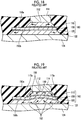
- FIG. 18 is a partial enlarged view of the semiconductor module disclosed in JP 2016-046497 A .
- a semiconductor chip 160 has a semiconductor substrate 150, a first electrode 110 in contact with one surface 150a of the semiconductor substrate 150, and a second electrode 120 in contact with the other surface 150b of the semiconductor substrate 150.
- the first electrode 110 is connected to a first conductor 114 by a solder layer 112 and the second electrode 120 is connected to a second conductor 124 by a solder layer 122.
- Each of the first conductor 114 and the second conductor 124 functions as a heat dissipation member releasing heat from the semiconductor substrate 150.
- An electrode (such as a signal electrode) other than the first electrode 110 is disposed on the surface 150a of the semiconductor substrate 150, and thus the first electrode 110 is smaller in size than the second electrode 120.
- Each of the first conductor 114, the second conductor 124, and the semiconductor substrate 150 thermally expands when the semiconductor substrate 150 generates heat.
- the expansion amount of the first conductor 114 and the expansion amount of the second conductor 124 exceed the expansion amount of the semiconductor substrate 150 since the linear expansion coefficient of the first conductor 114 and the linear expansion coefficient of the second conductor 124 are larger than the linear expansion coefficient of the semiconductor substrate 150.
- the solder layer 112 is pulled to the outer peripheral side due to the thermal expansion of the first conductor 114.
- solder layer 122 is pulled to the outer peripheral side due to the thermal expansion of the second conductor 124. Stress is repeatedly applied to the solder layers 112, 122 as the semiconductor substrate 150 repeatedly generates heat. Then, solder moves to the outer peripheral side in the solder layer 112 and solder moves to the outer peripheral side in the solder layer 122, as indicated by the arrows in FIG. 18 , due to the creep phenomenon of the solder. As the creep phenomenon of the solder continues, the solder moving to the outer peripheral side in the solder layer 112 pressurizes the semiconductor substrate 150 downward near an outer peripheral edge 110a of the first electrode 110 as indicated by the arrows 190 in FIG. 19 .
- the semiconductor substrate 150 warps downward at the outer peripheral edge 110a of the first electrode 110 as illustrated in FIG. 19 .
- the solder in the solder layer 122 moves from the pressurized part toward the surroundings.
- some of the solder in the solder layer 122 moves toward the lower portion of the middle portion of the first electrode 110 as indicated by the arrows 192 in FIG. 19 .
- the solder layer 122 pressurizes the semiconductor substrate 150 upward at the position of the middle portion of the first electrode 110 and the semiconductor substrate 150 warps upward. Degradation of the semiconductor substrate 150 results from the warpage of the semiconductor substrate 150 illustrated in FIG. 19 .
- this specification proposes a technique for suppressing semiconductor substrate warpage attributable to a creep phenomenon of solder in a semiconductor module.
- An aspect of the disclosure relates to a semiconductor module including a semiconductor substrate, a first electrode in contact with a first surface of the semiconductor substrate in a range except an outer peripheral region of the first surface of the semiconductor substrate, a second electrode in contact with a second surface of the semiconductor substrate, the first surface and the second surface being opposite surfaces of the semiconductor substrate, a first conductor connected to the first electrode via a first solder layer, and a second conductor connected to the second electrode via a second solder layer.
- the second electrode overlaps the entire first electrode and is wider than the first electrode when seen along a thickness direction of the semiconductor substrate.
- a recessed portion located along an outer peripheral edge of the first electrode is disposed in a joining surface of the second conductor in contact with the second solder layer to overlap the outer peripheral edge of the first electrode when the semiconductor substrate is seen along the thickness direction.
- the recessed portion located along the outer peripheral edge of the first electrode is disposed in the joining surface of the second conductor in contact with the second solder layer to overlap the outer peripheral edge of the first electrode when the semiconductor substrate is seen along the thickness direction. Since the second solder layer in the recessed portion (that is, the second solder layer below the outer peripheral edge of the first electrode) is thick, the second solder layer in the recessed portion has relatively high elasticity. Accordingly, even when the semiconductor substrate is pressurized downward below the outer peripheral edge of the first electrode due to the creep phenomenon of the first solder layer, a creep phenomenon is unlikely to occur in the second solder layer in the recessed portion.
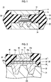
- a semiconductor module 10 As illustrated in FIG. 1 , a semiconductor module 10 according to an embodiment has an upper lead frame 12, a metal block 16, a semiconductor chip 20, a lower lead frame 24, and an insulating resin 26.
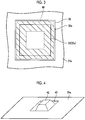
- the semiconductor chip 20 has a SiC substrate 30, an upper electrode 32, and a lower electrode 34.
- the upper electrode 32 is in contact with an upper surface 30a of the SiC substrate 30.
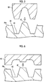
- FIG. 3 is a plan view showing the semiconductor chip 20 from above.
- the upper electrode 32 covers the middle portion of the upper surface 30a of the SiC substrate 30 and does not cover the outer peripheral portion of the upper surface 30a.
- a signal electrode (not illustrated) is disposed at a part of the outer peripheral portion of the upper surface 30a.
- the signal electrode is connected to a signal terminal (not illustrated) by a wire.
- the lower electrode 34 covers the whole area of a lower surface 30b of the SiC substrate 30.
- the lower electrode 34 (that is, the range that has the same size as the SiC substrate 30 in FIG. 3 ) overlaps the entire upper electrode 32 and is wider than the upper electrode 32.
- a semiconductor device such as a metal oxide semiconductor field effect transistor (MOSFET) for high current control and a diode is formed in the SiC substrate 30.
- MOSFET metal oxide semiconductor field effect transistor
- the metal block 16 is formed of a metal (more specifically, copper). As illustrated in FIGS. 1 and 2 , the metal block 16 is disposed above the semiconductor chip 20. The lower surface of the metal block 16 is connected to the upper electrode 32 of the semiconductor chip 20 by a first solder layer 18.
- the upper lead frame 12 is formed of a metal (more specifically, copper). As illustrated in FIG. 1 , the upper lead frame 12 is disposed above the metal block 16. The lower surface of the upper lead frame 12 is connected to the upper surface of the metal block 16 by a solder layer 14.
- the lower lead frame 24 is formed of a metal (more specifically, copper). As illustrated in FIGS. 1 and 2 , the lower lead frame 24 is disposed below the semiconductor chip 20. An upper surface 24a of the lower lead frame 24 is connected to the lower electrode 34 of the semiconductor chip 20 by a second solder layer 22. The upper surface 24a of the lower lead frame 24 has a recessed portion 40 and a projecting portion 42. As illustrated in FIGS. 3 and 4 , the recessed portion 40 surrounds the projection portion in the upper surface 24a. In FIG. 3 , the range in which the recessed portion 40 is disposed is indicated by a diagonal line. When seen along the thickness direction of the SiC substrate 30 as in FIG.
- the projecting portion 42 is disposed in a range surrounded by the recessed portion 40. As illustrated in FIGS. 2 and 4 , the projecting portion 42 protrudes upward beyond the upper surface 24a on the outer peripheral side of the recessed portion 40.
- the whole of the recessed portion 40 and the projecting portion 42 is covered with the second solder layer 22.
- the second solder layer 22 is joined to the surface of the projecting portion 42, the inner surface of the recessed portion 40, and the upper surface 24a on the outer peripheral side of the recessed portion 40 (upper surface 24a near the recessed portion 40).
- a laminate of the upper lead frame 12, the metal block 16, the semiconductor chip 20, and the lower lead frame 24 is covered by the insulating resin 26.
- the entire surface of the laminate except the upper surface of the upper lead frame 12 and the lower surface of the lower lead frame 24 is covered by the insulating resin 26.
- the upper surface of the upper lead frame 12 and the lower surface of the lower lead frame 24 are connected to a cooler (not illustrated).
- the upper lead frame 12 and the lower lead frame 24 function as wiring of the semiconductor module 10.
- a current is allowed to flow to the semiconductor chip 20 via the upper lead frame 12 and the lower lead frame 24.
- the upper lead frame 12 and the lower lead frame 24 also function as a heat sink. Once a current flows to the semiconductor chip 20, the semiconductor chip 20 generates heat. The heat generated by the semiconductor chip 20 is dissipated via the lower lead frame 24 and dissipated via the metal block 16 and the upper lead frame 12. Accordingly, once a current flows to the semiconductor chip 20, the temperatures of the lower lead frame 24, the metal block 16, and the upper lead frame 12 become relatively high.
- the linear expansion coefficient of the lower lead frame 24 and the linear expansion coefficient of the metal block 16 are higher than the linear expansion coefficient of the SiC substrate 30.
- the expansion amounts of the lower lead frame 24 and the metal block 16 exceed the expansion amount of the SiC substrate 30. Since the expansion amount of the SiC substrate 30 is small and the expansion amount of the lower lead frame 24 is large, high thermal stress is applied to the second solder layer 22 between the SiC substrate 30 and the lower lead frame 24. Accordingly, once the semiconductor chip 20 is repeatedly energized, thermal stress is repeatedly applied to the second solder layer 22 and the solder in the second solder layer 22 moves toward the outer peripheral side due to the creep phenomenon of the solder. Since the expansion amount of the SiC substrate 30 is small and the expansion amount of the metal block 16 is large, high thermal stress is applied to the first solder layer 18 between the SiC substrate 30 and the metal block 16.
- thermal stress is repeatedly applied to the first solder layer 18 and the solder in the first solder layer 18 moves toward the outer peripheral side due to the creep phenomenon of the solder.
- the solder in the first solder layer 18 moves toward the outer peripheral side, pressure increases at the outer peripheral edge of the first solder layer 18 (that is, near the outer peripheral edge 32a of the upper electrode 32).
- the first solder layer 18 pressurizes the SiC substrate 30 downward near the outer peripheral edge 32a of the upper electrode 32.
- the pressure is applied to the second solder layer 22 below the outer peripheral edge 32a of the upper electrode 32.
- the recessed portion 40 is disposed below the outer peripheral edge 32a of the upper electrode 32, the pressure is applied to the second solder layer 22 in the recessed portion 40. Since the second solder layer 22 in the recessed portion 40 is thick, the second solder layer 22 in the recessed portion 40 has relatively high elasticity and is unlikely to be plastically deformed. Accordingly, even when pressure is repeatedly applied to the second solder layer 22 in the recessed portion 40, a solder movement attributable to the pressure is unlikely to occur. Since the lower lead frame 24 has the projecting portion 42, a movement of the solder in the second solder layer 22 toward the middle portion is hindered by the side surfaces of the projecting portion 42.
- a simulation result will be described below with regard to the warpage of the SiC substrate 30 at a time when a predetermined number of thermal cycles were applied.
- a semiconductor module (Sample 1) in which the lower lead frame 24 does not have the recessed portion 40 and the projecting portion 42 (that is, a semiconductor module in which the upper surface 24a of the lower lead frame 24 is flat as in the related art) has resulted in a warpage of approximately 6.82 ⁇ 10 -4 mm in the SiC substrate 30.
- SiC substrates are especially prone to warpage as described above because general SiC substrates are extremely thin with a thickness of 150 ⁇ m or less.
- a semiconductor module (Sample 2) in which the lower lead frame 24 has the recessed portion 40 and does not have the projecting portion 42 has resulted in a warpage of approximately 3.78 ⁇ 10 -4 mm in the SiC substrate 30 under the same conditions as Sample 1. Comparison between Samples 1 and 2 clearly shows that warpage of the SiC substrate 30 can be effectively suppressed by the recessed portion 40 being provided.
- a semiconductor module (Sample 3) in which the lower lead frame 24 has the recessed portion 40 and the projecting portion 42 (that is, the configuration of FIGS. 1 and 2 ) has resulted in a warpage of approximately 1.74 ⁇ 10 -4 mm in the SiC substrate 30 under the same conditions as Sample 2. Comparison between Samples 2 and 3 clearly shows that warpage of the SiC substrate 30 can be more effectively suppressed by the projecting portion 42 being provided.
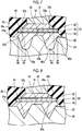
- Steps in which the recessed portion 40 and the projecting portion 42 are formed are illustrated in FIGS. 5 and 6 .
- the flat upper surface 24a of the lower lead frame 24 that is yet to be processed is pressed by a mold 90 illustrated in FIG. 5 .
- the recessed portion 40 and the projecting portion 42 are formed.
- the upper surface of the projecting portion 42 is curved and protuberant.
- the outer peripheral edge of the recessed portion 40 has a burr 94.
- the upper surface of the projecting portion 42 and the burr 94 are pressed by a mold 92 illustrated in FIG. 6 .
- the upper surface of the projecting portion 42 is flattened and the burr 94 disappears.
- the semiconductor module according to the modification example to be described below has the same configuration as the semiconductor module 10 according to the above-described embodiment except particularly mentioned parts.
- FIG. 7 shows the sectional shape of the recessed portion 40 according to the modification example.
- the recessed portion 40 has a U-shaped cross section.
- a deepest portion 40a of the recessed portion 40 is positioned on the inner peripheral side of the outer peripheral edge 32a of the upper electrode 32 (more specifically, the deepest portion 40a is positioned on the inner peripheral side of the outer peripheral edge 32a of the upper electrode 32 when the SiC substrate 30 is seen along the thickness direction).
- a simulation similar to Sample 1 described above was performed with the configuration of the semiconductor module illustrated in FIG.
- Example 4 the simulation has resulted in a warpage of approximately 2.35 ⁇ 10 -4 mm in the SiC substrate 30.
- a simulation similar to Sample 4 described above was performed with a configuration in which the deepest portion 40a is positioned on the outer peripheral side of the outer peripheral edge 32a of the upper electrode 32 (Sample 5), and the simulation has resulted in a warpage of approximately 2.49 ⁇ 10 -4 mm in the SiC substrate.
- Comparison between Samples 4 and 5 clearly shows that warpage of the SiC substrate 30 can be further suppressed by the deepest portion 40a of the recessed portion 40 being disposed on the inner peripheral side of the outer peripheral edge 32a of the upper electrode 32.
- an outer peripheral edge 40b of the recessed portion 40 is positioned on the inner peripheral side of an outer peripheral edge 30c of the SiC substrate 30 (more specifically, the outer peripheral edge 40b is positioned on the inner peripheral side of the outer peripheral edge 30c when the SiC substrate 30 is seen along the thickness direction).
- the warpage of the SiC substrate 30 in the configuration of FIG. 7 (that is, Sample 4) is 2.35 ⁇ 10 -4 mm as described above.
- the recessed portion 40 may have a V-like sectional shape as in FIG. 8 .
- the recessed portion 40 may have a rectangular sectional shape as in FIG. 9 .
- the recessed portion 40 may have a stepwise sectional shape as in FIG. 10 .
- the metal block 16 and the upper lead frame 12 are connected by the solder layer 14.
- the semiconductor module may be configured by means of a metal part 19 shaped such that the metal block 16 and the upper lead frame 12 are integrated as illustrated in FIG. 11 .
- the upper lead frame 12 may be connected to the upper electrode of the semiconductor chip 20 via the first solder layer 18 and without the metal block 16.
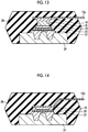
- a terminal 12a thinner than the upper lead frame 12 may be connected to the upper surface of the metal block 16.
- a thin terminal 12b may be connected to the upper electrode of the semiconductor chip 20 not via the metal block 16.
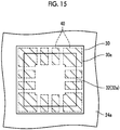
- the recessed portion 40 has a frame shape surrounding a range in the upper surface 24a of the lower lead frame 24.
- the recessed portion 40 may not have a frame shape insofar as the recessed portion 40 is disposed along the lower portion of the outer peripheral edge 32a of the upper electrode 32.
- the recessed portions 40 may be intermittently distributed along the lower portion of the outer peripheral edge 32a of the upper electrode 32.
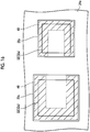
- a partially interrupted recessed portion 40 may extend along the lower portion of the outer peripheral edge 32a of the upper electrode 32. In the configuration that is illustrated in FIG.
- two semiconductor chips 20x, 20y are mounted on the lower lead frame 24.
- the semiconductor chip 20x may constitute a MOSFET and the semiconductor chip 20y may constitute a diode.
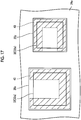
- the recessed portion 40 may not be provided on the sides of the upper electrode 32 of the semiconductor chip 20x and the upper electrode 32 of the semiconductor chip 20y that face each other. As illustrated in FIG. 17 , the recessed portion 40 may be interrupted.
- a part of the recessed portion 40 may not be covered with the second solder layer 22.
- the semiconductor chip 20 is covered with the insulating resin 26 in the embodiment described above, the semiconductor chip 20 may not be covered with the insulating resin 26.
- the semiconductor chip 20 may be covered with silicon gel or the like instead of the insulating resin 26.
- the upper electrode according to the embodiment is an example of a first electrode according to the disclosure.
- the lower electrode according to the embodiment is an example of a second electrode according to the disclosure.
- the upper lead frame according to the embodiment is an example of a first conductor according to the disclosure.
- the lower lead frame according to the embodiment is an example of a second conductor according to the disclosure.
- the projecting portion according to the embodiment is an example of a joining surface in a range surrounded by a recessed portion according to the disclosure.
- the recessed portion may have a frame shape in the joining surface.
- the entire outer peripheral edge of the first electrode may overlap the recessed portion when the semiconductor substrate is seen along the thickness direction.
- warpage of the semiconductor substrate can be more desirably suppressed.
- the joining surface in a range surrounded by the recessed portion may protrude to the semiconductor substrate side beyond a surface of the second conductor on an outer peripheral side of the recessed portion.
- warpage of the semiconductor substrate can be more desirably suppressed.
- a deepest portion of the recessed portion may be positioned on an inner peripheral side of the outer peripheral edge of the first electrode when the semiconductor substrate is seen along the thickness direction.
- warpage of the semiconductor substrate can be more desirably suppressed.
- the second solder layer may cover the recessed portion and the surface of the second conductor on the outer peripheral side of the recessed portion.
- a semiconductor module (10) includes a semiconductor substrate (30), a first electrode (32) in contact with a first surface of the semiconductor substrate (30), a second electrode (34) in contact with a second surface of the semiconductor substrate (30), a first conductor (12) connected to the first electrode (32) via a first solder layer (18), and a second conductor (24) connected to the second electrode (34) via a second solder layer (22).
- the second electrode overlaps the entire first electrode and is wider than the first electrode when seen along a thickness direction of the semiconductor substrate.
- a recessed portion (40) located along an outer peripheral edge of the first electrode is disposed in a joining surface of the second conductor in contact with the second solder layer to overlap the outer peripheral edge of the first electrode when the semiconductor substrate is seen along the thickness direction.
Landscapes
- Cooling Or The Like Of Semiconductors Or Solid State Devices (AREA)
- Physics & Mathematics (AREA)
- Geometry (AREA)
- Die Bonding (AREA)
- Structures Or Materials For Encapsulating Or Coating Semiconductor Devices Or Solid State Devices (AREA)
- Chemical & Material Sciences (AREA)
- Engineering & Computer Science (AREA)
- Ceramic Engineering (AREA)
Abstract
Description
- The technique that is disclosed in this specification relates to a semiconductor module.
- Japanese Unexamined Patent Application Publication No.
2016-046497 JP 2016-046497 A FIG. 18 is a partial enlarged view of the semiconductor module disclosed inJP 2016-046497 A FIG. 18 , asemiconductor chip 160 has asemiconductor substrate 150, afirst electrode 110 in contact with onesurface 150a of thesemiconductor substrate 150, and asecond electrode 120 in contact with theother surface 150b of thesemiconductor substrate 150. Thefirst electrode 110 is connected to afirst conductor 114 by asolder layer 112 and thesecond electrode 120 is connected to asecond conductor 124 by asolder layer 122. Each of thefirst conductor 114 and thesecond conductor 124 functions as a heat dissipation member releasing heat from thesemiconductor substrate 150. - An electrode (such as a signal electrode) other than the
first electrode 110 is disposed on thesurface 150a of thesemiconductor substrate 150, and thus thefirst electrode 110 is smaller in size than thesecond electrode 120. Each of thefirst conductor 114, thesecond conductor 124, and thesemiconductor substrate 150 thermally expands when thesemiconductor substrate 150 generates heat. At that time, the expansion amount of thefirst conductor 114 and the expansion amount of thesecond conductor 124 exceed the expansion amount of thesemiconductor substrate 150 since the linear expansion coefficient of thefirst conductor 114 and the linear expansion coefficient of thesecond conductor 124 are larger than the linear expansion coefficient of thesemiconductor substrate 150. Thesolder layer 112 is pulled to the outer peripheral side due to the thermal expansion of thefirst conductor 114. Thesolder layer 122 is pulled to the outer peripheral side due to the thermal expansion of thesecond conductor 124. Stress is repeatedly applied to thesolder layers semiconductor substrate 150 repeatedly generates heat. Then, solder moves to the outer peripheral side in thesolder layer 112 and solder moves to the outer peripheral side in thesolder layer 122, as indicated by the arrows inFIG. 18 , due to the creep phenomenon of the solder. As the creep phenomenon of the solder continues, the solder moving to the outer peripheral side in thesolder layer 112 pressurizes thesemiconductor substrate 150 downward near an outerperipheral edge 110a of thefirst electrode 110 as indicated by thearrows 190 inFIG. 19 . As a result, thesemiconductor substrate 150 warps downward at the outerperipheral edge 110a of thefirst electrode 110 as illustrated inFIG. 19 . As a result of pressurization by thesemiconductor substrate 150 that is warped downward, the solder in thesolder layer 122 moves from the pressurized part toward the surroundings. As a result, some of the solder in thesolder layer 122 moves toward the lower portion of the middle portion of thefirst electrode 110 as indicated by thearrows 192 inFIG. 19 . Accordingly, thesolder layer 122 pressurizes thesemiconductor substrate 150 upward at the position of the middle portion of thefirst electrode 110 and thesemiconductor substrate 150 warps upward. Degradation of thesemiconductor substrate 150 results from the warpage of thesemiconductor substrate 150 illustrated inFIG. 19 . Then, the reliability of the semiconductor module is reduced. Although thesemiconductor chip 160 is covered with insulating resin inFIGS. 18 and 19 , it has been confirmed that warpage as inFIG. 19 occurs even in a case where the semiconductor chip is not covered with insulating resin. Therefore, this specification proposes a technique for suppressing semiconductor substrate warpage attributable to a creep phenomenon of solder in a semiconductor module. - An aspect of the disclosure relates to a semiconductor module including a semiconductor substrate, a first electrode in contact with a first surface of the semiconductor substrate in a range except an outer peripheral region of the first surface of the semiconductor substrate, a second electrode in contact with a second surface of the semiconductor substrate, the first surface and the second surface being opposite surfaces of the semiconductor substrate, a first conductor connected to the first electrode via a first solder layer, and a second conductor connected to the second electrode via a second solder layer. The second electrode overlaps the entire first electrode and is wider than the first electrode when seen along a thickness direction of the semiconductor substrate. A recessed portion located along an outer peripheral edge of the first electrode is disposed in a joining surface of the second conductor in contact with the second solder layer to overlap the outer peripheral edge of the first electrode when the semiconductor substrate is seen along the thickness direction.
- In the semiconductor module, the recessed portion located along the outer peripheral edge of the first electrode is disposed in the joining surface of the second conductor in contact with the second solder layer to overlap the outer peripheral edge of the first electrode when the semiconductor substrate is seen along the thickness direction. Since the second solder layer in the recessed portion (that is, the second solder layer below the outer peripheral edge of the first electrode) is thick, the second solder layer in the recessed portion has relatively high elasticity. Accordingly, even when the semiconductor substrate is pressurized downward below the outer peripheral edge of the first electrode due to the creep phenomenon of the first solder layer, a creep phenomenon is unlikely to occur in the second solder layer in the recessed portion. Accordingly, pressure on the semiconductor substrate attributable to the creep phenomenon of the second solder layer is unlikely to be generated and warpage of the semiconductor substrate can be suppressed. Therefore, in the semiconductor module according to the aspect of the disclosure, time degradation of the semiconductor substrate is unlikely to occur.
- Features, advantages, and technical and industrial significance of exemplary embodiments of the invention will be described below with reference to the accompanying drawings, in which like numerals denote like elements, and wherein:
-
FIG. 1 is a sectional view of a semiconductor module; -
FIG. 2 is an enlarged sectional view of a semiconductor chip and the surroundings thereof; -
FIG. 3 is a plan view showing the semiconductor chip from above; -
FIG. 4 is a perspective view of a recessed portion and a projecting portion; -
FIG. 5 is an explanatory drawing of a step in which the recessed portion and the projecting portion are formed; -
FIG. 6 is an explanatory drawing of a step in which the recessed portion and the projecting portion are formed; -
FIG. 7 is an enlarged sectional view of a semiconductor module according to a modification example that corresponds toFIG. 2 ; -
FIG. 8 is an enlarged sectional view of a semiconductor module according to a modification example that corresponds toFIG. 2 ; -
FIG. 9 is an enlarged sectional view of a semiconductor module according to a modification example that corresponds toFIG. 2 ; -
FIG. 10 is an enlarged sectional view of a semiconductor module according to a modification example that corresponds toFIG. 2 ; -
FIG. 11 is a sectional view of a semiconductor module according to a modification example that corresponds toFIG. 1 ; -
FIG. 12 is a sectional view of a semiconductor module according to a modification example that corresponds toFIG. 1 ; -
FIG. 13 is a sectional view of a semiconductor module according to a modification example that corresponds toFIG. 1 ; -
FIG. 14 is a sectional view of a semiconductor module according to a modification example that corresponds toFIG. 1 ; -
FIG. 15 is a plan view of a semiconductor module according to a modification example that corresponds toFIG. 3 ; -
FIG. 16 is a sectional view of a semiconductor module according to a modification example that corresponds toFIG. 3 ; -
FIG. 17 is a sectional view of a semiconductor module according to a modification example that corresponds toFIG. 3 ; -
FIG. 18 is an enlarged sectional view of a semiconductor chip of a semiconductor module according to the related art and the surroundings thereof; and -
FIG. 19 is an enlarged sectional view of the semiconductor chip of the semiconductor module according to the related art and the surroundings thereof. - As illustrated in
FIG. 1 , asemiconductor module 10 according to an embodiment has anupper lead frame 12, ametal block 16, asemiconductor chip 20, alower lead frame 24, and aninsulating resin 26. - As illustrated in
FIG. 2 , thesemiconductor chip 20 has aSiC substrate 30, anupper electrode 32, and alower electrode 34. Theupper electrode 32 is in contact with anupper surface 30a of theSiC substrate 30.FIG. 3 is a plan view showing thesemiconductor chip 20 from above. As illustrated inFIG. 3 , theupper electrode 32 covers the middle portion of theupper surface 30a of theSiC substrate 30 and does not cover the outer peripheral portion of theupper surface 30a. A signal electrode (not illustrated) is disposed at a part of the outer peripheral portion of theupper surface 30a. The signal electrode is connected to a signal terminal (not illustrated) by a wire. As illustrated inFIG. 2 , thelower electrode 34 covers the whole area of alower surface 30b of theSiC substrate 30. Accordingly, when seen along the thickness direction of theSiC substrate 30 as inFIG. 3 , the lower electrode 34 (that is, the range that has the same size as theSiC substrate 30 inFIG. 3 ) overlaps the entireupper electrode 32 and is wider than theupper electrode 32. A semiconductor device such as a metal oxide semiconductor field effect transistor (MOSFET) for high current control and a diode is formed in theSiC substrate 30. - The
metal block 16 is formed of a metal (more specifically, copper). As illustrated inFIGS. 1 and 2 , themetal block 16 is disposed above thesemiconductor chip 20. The lower surface of themetal block 16 is connected to theupper electrode 32 of thesemiconductor chip 20 by afirst solder layer 18. - The
upper lead frame 12 is formed of a metal (more specifically, copper). As illustrated inFIG. 1 , theupper lead frame 12 is disposed above themetal block 16. The lower surface of theupper lead frame 12 is connected to the upper surface of themetal block 16 by asolder layer 14. - The
lower lead frame 24 is formed of a metal (more specifically, copper). As illustrated inFIGS. 1 and 2 , thelower lead frame 24 is disposed below thesemiconductor chip 20. Anupper surface 24a of thelower lead frame 24 is connected to thelower electrode 34 of thesemiconductor chip 20 by asecond solder layer 22. Theupper surface 24a of thelower lead frame 24 has a recessedportion 40 and a projectingportion 42. As illustrated inFIGS. 3 and 4 , the recessedportion 40 surrounds the projection portion in theupper surface 24a. InFIG. 3 , the range in which the recessedportion 40 is disposed is indicated by a diagonal line. When seen along the thickness direction of theSiC substrate 30 as inFIG. 3 , the whole of an outerperipheral edge 32a of theupper electrode 32 overlaps the recessedportion 40. The projectingportion 42 is disposed in a range surrounded by the recessedportion 40. As illustrated inFIGS. 2 and4 , the projectingportion 42 protrudes upward beyond theupper surface 24a on the outer peripheral side of the recessedportion 40. The whole of the recessedportion 40 and the projectingportion 42 is covered with thesecond solder layer 22. Thesecond solder layer 22 is joined to the surface of the projectingportion 42, the inner surface of the recessedportion 40, and theupper surface 24a on the outer peripheral side of the recessed portion 40 (upper surface 24a near the recessed portion 40). - As illustrated in
FIG. 1 , a laminate of theupper lead frame 12, themetal block 16, thesemiconductor chip 20, and thelower lead frame 24 is covered by the insulatingresin 26. The entire surface of the laminate except the upper surface of theupper lead frame 12 and the lower surface of thelower lead frame 24 is covered by the insulatingresin 26. The upper surface of theupper lead frame 12 and the lower surface of thelower lead frame 24 are connected to a cooler (not illustrated). - The
upper lead frame 12 and thelower lead frame 24 function as wiring of thesemiconductor module 10. A current is allowed to flow to thesemiconductor chip 20 via theupper lead frame 12 and thelower lead frame 24. Theupper lead frame 12 and thelower lead frame 24 also function as a heat sink. Once a current flows to thesemiconductor chip 20, thesemiconductor chip 20 generates heat. The heat generated by thesemiconductor chip 20 is dissipated via thelower lead frame 24 and dissipated via themetal block 16 and theupper lead frame 12. Accordingly, once a current flows to thesemiconductor chip 20, the temperatures of thelower lead frame 24, themetal block 16, and theupper lead frame 12 become relatively high. The linear expansion coefficient of thelower lead frame 24 and the linear expansion coefficient of themetal block 16 are higher than the linear expansion coefficient of theSiC substrate 30. Accordingly, the expansion amounts of thelower lead frame 24 and themetal block 16 exceed the expansion amount of theSiC substrate 30. Since the expansion amount of theSiC substrate 30 is small and the expansion amount of thelower lead frame 24 is large, high thermal stress is applied to thesecond solder layer 22 between theSiC substrate 30 and thelower lead frame 24. Accordingly, once thesemiconductor chip 20 is repeatedly energized, thermal stress is repeatedly applied to thesecond solder layer 22 and the solder in thesecond solder layer 22 moves toward the outer peripheral side due to the creep phenomenon of the solder. Since the expansion amount of theSiC substrate 30 is small and the expansion amount of themetal block 16 is large, high thermal stress is applied to thefirst solder layer 18 between theSiC substrate 30 and themetal block 16. Accordingly, once thesemiconductor chip 20 is repeatedly energized, thermal stress is repeatedly applied to thefirst solder layer 18 and the solder in thefirst solder layer 18 moves toward the outer peripheral side due to the creep phenomenon of the solder. Once the solder in thefirst solder layer 18 moves toward the outer peripheral side, pressure increases at the outer peripheral edge of the first solder layer 18 (that is, near the outerperipheral edge 32a of the upper electrode 32). Accordingly, thefirst solder layer 18 pressurizes theSiC substrate 30 downward near the outerperipheral edge 32a of theupper electrode 32. The pressure is applied to thesecond solder layer 22 below the outerperipheral edge 32a of theupper electrode 32. Since the recessedportion 40 is disposed below the outerperipheral edge 32a of theupper electrode 32, the pressure is applied to thesecond solder layer 22 in the recessedportion 40. Since thesecond solder layer 22 in the recessedportion 40 is thick, thesecond solder layer 22 in the recessedportion 40 has relatively high elasticity and is unlikely to be plastically deformed. Accordingly, even when pressure is repeatedly applied to thesecond solder layer 22 in the recessedportion 40, a solder movement attributable to the pressure is unlikely to occur. Since thelower lead frame 24 has the projectingportion 42, a movement of the solder in thesecond solder layer 22 toward the middle portion is hindered by the side surfaces of the projectingportion 42. Accordingly, in thesecond solder layer 22, a solder movement toward the middle portion as indicated by thearrows 192 inFIG. 19 rarely occurs. Accordingly, in thesemiconductor module 10 according to the embodiment, pressure with which thesecond solder layer 22 pushes the middle portion of theSiC substrate 30 upward is unlikely to be generated. Accordingly, in thesemiconductor module 10 according to the embodiment, semiconductor substrate warpage as inFIG. 19 is suppressed. Therefore, in thesemiconductor module 10, time degradation of theSiC substrate 30 can be suppressed and high reliability can be maintained. - A simulation result will be described below with regard to the warpage of the
SiC substrate 30 at a time when a predetermined number of thermal cycles were applied. A semiconductor module (Sample 1) in which thelower lead frame 24 does not have the recessedportion 40 and the projecting portion 42 (that is, a semiconductor module in which theupper surface 24a of thelower lead frame 24 is flat as in the related art) has resulted in a warpage of approximately 6.82 × 10⁻⁴ mm in theSiC substrate 30. SiC substrates are especially prone to warpage as described above because general SiC substrates are extremely thin with a thickness of 150 µm or less. A semiconductor module (Sample 2) in which thelower lead frame 24 has the recessedportion 40 and does not have the projectingportion 42 has resulted in a warpage of approximately 3.78 × 10⁻⁴ mm in theSiC substrate 30 under the same conditions asSample 1. Comparison betweenSamples 1 and 2 clearly shows that warpage of theSiC substrate 30 can be effectively suppressed by the recessedportion 40 being provided. A semiconductor module (Sample 3) in which thelower lead frame 24 has the recessedportion 40 and the projecting portion 42 (that is, the configuration ofFIGS. 1 and 2 ) has resulted in a warpage of approximately 1.74 × 10⁻⁴ mm in theSiC substrate 30 under the same conditions as Sample 2. Comparison between Samples 2 and 3 clearly shows that warpage of theSiC substrate 30 can be more effectively suppressed by the projectingportion 42 being provided. - Steps in which the recessed
portion 40 and the projectingportion 42 are formed are illustrated inFIGS. 5 and 6 . Firstly, the flatupper surface 24a of thelower lead frame 24 that is yet to be processed is pressed by amold 90 illustrated inFIG. 5 . As a result, the recessedportion 40 and the projectingportion 42 are formed. In the stage ofFIG. 5 , the upper surface of the projectingportion 42 is curved and protuberant. In the stage ofFIG. 5 , the outer peripheral edge of the recessedportion 40 has aburr 94. The upper surface of the projectingportion 42 and theburr 94 are pressed by amold 92 illustrated inFIG. 6 . As a result, the upper surface of the projectingportion 42 is flattened and theburr 94 disappears. - A modification example will be described below. The semiconductor module according to the modification example to be described below has the same configuration as the
semiconductor module 10 according to the above-described embodiment except particularly mentioned parts. - The sectional shape of the recessed
portion 40 can be appropriately changed.FIG. 7 shows the sectional shape of the recessedportion 40 according to the modification example. InFIG. 7 , the recessedportion 40 has a U-shaped cross section. As indicated by thearrows 96, inFIG. 7 , adeepest portion 40a of the recessedportion 40 is positioned on the inner peripheral side of the outerperipheral edge 32a of the upper electrode 32 (more specifically, thedeepest portion 40a is positioned on the inner peripheral side of the outerperipheral edge 32a of theupper electrode 32 when theSiC substrate 30 is seen along the thickness direction). A simulation similar toSample 1 described above was performed with the configuration of the semiconductor module illustrated inFIG. 7 (Sample 4), and the simulation has resulted in a warpage of approximately 2.35 × 10⁻⁴ mm in theSiC substrate 30. A simulation similar to Sample 4 described above was performed with a configuration in which thedeepest portion 40a is positioned on the outer peripheral side of the outerperipheral edge 32a of the upper electrode 32 (Sample 5), and the simulation has resulted in a warpage of approximately 2.49 × 10⁻⁴ mm in the SiC substrate. Comparison between Samples 4 and 5 clearly shows that warpage of theSiC substrate 30 can be further suppressed by thedeepest portion 40a of the recessedportion 40 being disposed on the inner peripheral side of the outerperipheral edge 32a of theupper electrode 32. - As indicated by the
arrows 98, inFIG. 7 , an outerperipheral edge 40b of the recessedportion 40 is positioned on the inner peripheral side of an outer peripheral edge 30c of the SiC substrate 30 (more specifically, the outerperipheral edge 40b is positioned on the inner peripheral side of the outer peripheral edge 30c when theSiC substrate 30 is seen along the thickness direction). The warpage of theSiC substrate 30 in the configuration ofFIG. 7 (that is, Sample 4) is 2.35 × 10⁻⁴ mm as described above. A simulation similar to Sample 4 described above was performed with a configuration in which the outerperipheral edge 40b of the recessedportion 40 is positioned on the outer peripheral side of the outer peripheral edge 30c of the SiC substrate 30 (Sample 6), and the simulation has resulted in a warpage of approximately 4.56 × 10⁻⁴ mm in theSiC substrate 30. Comparison between Samples 4 and 6 clearly shows that warpage of theSiC substrate 30 can be further suppressed by the outerperipheral edge 40b of the recessedportion 40 being disposed on the inner peripheral side of the outer peripheral edge 30c of theSiC substrate 30. - The recessed
portion 40 may have a V-like sectional shape as inFIG. 8 . The recessedportion 40 may have a rectangular sectional shape as inFIG. 9 . The recessedportion 40 may have a stepwise sectional shape as inFIG. 10 . - In
FIG. 1 , themetal block 16 and theupper lead frame 12 are connected by thesolder layer 14. Alternatively, the semiconductor module may be configured by means of ametal part 19 shaped such that themetal block 16 and theupper lead frame 12 are integrated as illustrated inFIG. 11 . As illustrated inFIG. 12 , theupper lead frame 12 may be connected to the upper electrode of thesemiconductor chip 20 via thefirst solder layer 18 and without themetal block 16. As illustrated inFIG. 13 , a terminal 12a thinner than theupper lead frame 12 may be connected to the upper surface of themetal block 16. As illustrated inFIG. 14 , athin terminal 12b may be connected to the upper electrode of thesemiconductor chip 20 not via themetal block 16. - As illustrated in
FIG. 4 , in thesemiconductor module 10 according to the embodiment described above, the recessedportion 40 has a frame shape surrounding a range in theupper surface 24a of thelower lead frame 24. Alternatively, the recessedportion 40 may not have a frame shape insofar as the recessedportion 40 is disposed along the lower portion of the outerperipheral edge 32a of theupper electrode 32. For example, as illustrated inFIG. 15 , the recessedportions 40 may be intermittently distributed along the lower portion of the outerperipheral edge 32a of theupper electrode 32. As illustrated inFIG. 16 , a partially interrupted recessedportion 40 may extend along the lower portion of the outerperipheral edge 32a of theupper electrode 32. In the configuration that is illustrated inFIG. 16 , twosemiconductor chips lower lead frame 24. For example, thesemiconductor chip 20x may constitute a MOSFET and thesemiconductor chip 20y may constitute a diode. In this case, the recessedportion 40 may not be provided on the sides of theupper electrode 32 of thesemiconductor chip 20x and theupper electrode 32 of thesemiconductor chip 20y that face each other. As illustrated inFIG. 17 , the recessedportion 40 may be interrupted. - Although the entire recessed
portion 40 is covered with thesecond solder layer 22 in the embodiment described above, a part of the recessedportion 40 may not be covered with thesecond solder layer 22. - Although the
semiconductor chip 20 is covered with the insulatingresin 26 in the embodiment described above, thesemiconductor chip 20 may not be covered with the insulatingresin 26. Thesemiconductor chip 20 may be covered with silicon gel or the like instead of the insulatingresin 26. - Relationships between the components of the semiconductor module according to the embodiment described above and the components of the semiconductor module according to the disclosure will be described below. The upper electrode according to the embodiment is an example of a first electrode according to the disclosure. The lower electrode according to the embodiment is an example of a second electrode according to the disclosure. The upper lead frame according to the embodiment is an example of a first conductor according to the disclosure. The lower lead frame according to the embodiment is an example of a second conductor according to the disclosure. The projecting portion according to the embodiment is an example of a joining surface in a range surrounded by a recessed portion according to the disclosure.
- Technical elements disclosed in this specification will be listed below. Each of the following technical elements is independently useful.
- In the semiconductor module according to an example disclosed in this specification, the recessed portion may have a frame shape in the joining surface. The entire outer peripheral edge of the first electrode may overlap the recessed portion when the semiconductor substrate is seen along the thickness direction.
- According to the above configuration, warpage of the semiconductor substrate can be more desirably suppressed.
- In the semiconductor module according to the example disclosed in this specification, the joining surface in a range surrounded by the recessed portion may protrude to the semiconductor substrate side beyond a surface of the second conductor on an outer peripheral side of the recessed portion.
- According to the above configuration, warpage of the semiconductor substrate can be more desirably suppressed.
- In the semiconductor module according to the example disclosed in this specification, a deepest portion of the recessed portion may be positioned on an inner peripheral side of the outer peripheral edge of the first electrode when the semiconductor substrate is seen along the thickness direction.
- According to the above configuration, warpage of the semiconductor substrate can be more desirably suppressed.
- In the semiconductor module according to the example disclosed in this specification, the second solder layer may cover the recessed portion and the surface of the second conductor on the outer peripheral side of the recessed portion.
- The embodiment described in detail above is merely an example and does not limit the scope of claims. The technique disclosed in the scope of claims includes various modifications and changes based on the specific example described above. The technical elements described in this specification or the drawings demonstrate technical utility independently or through various combinations and are not limited to the combinations disclosed in the filed claims. The technique exemplified in this specification or the drawings achieves multiple purposes at the same time and retains technical utility even when merely one of the purposes is achieved.
- A semiconductor module (10) includes a semiconductor substrate (30), a first electrode (32) in contact with a first surface of the semiconductor substrate (30), a second electrode (34) in contact with a second surface of the semiconductor substrate (30), a first conductor (12) connected to the first electrode (32) via a first solder layer (18), and a second conductor (24) connected to the second electrode (34) via a second solder layer (22). The second electrode overlaps the entire first electrode and is wider than the first electrode when seen along a thickness direction of the semiconductor substrate. A recessed portion (40) located along an outer peripheral edge of the first electrode is disposed in a joining surface of the second conductor in contact with the second solder layer to overlap the outer peripheral edge of the first electrode when the semiconductor substrate is seen along the thickness direction.
Claims (8)
- A semiconductor module (10) comprising:a semiconductor substrate (30);a first electrode (32) in contact with a first surface of the semiconductor substrate (30) in a range except an outer peripheral region of the first surface of the semiconductor substrate (30);a second electrode (34) in contact with a second surface of the semiconductor substrate (30), the first surface and the second surface being opposite surfaces of the semiconductor substrate (30);a first conductor (12) connected to the first electrode (32) via a first solder layer (18); anda second conductor (24) connected to the second electrode (34) via a second solder layer (22), wherein:the second electrode (34) overlaps the entire first electrode (32) and is wider than the first electrode (32) when seen along a thickness direction of the semiconductor substrate (30); anda recessed portion (40) located along an outer peripheral edge of the first electrode (32) is disposed in a joining surface of the second conductor (24) in contact with the second solder layer (22) to overlap the outer peripheral edge of the first electrode (32) when the semiconductor substrate (30) is seen along the thickness direction.
- The semiconductor module (10) according to claim 1, wherein:the recessed portion (40) surrounds a range in the joining surface; andthe entire outer peripheral edge of the first electrode (32) overlaps the recessed portion (40) when the semiconductor substrate (30) is seen along the thickness direction.
- The semiconductor module (10) according to claim 2, wherein the joining surface (42) in the range surrounded by the recessed portion (40) protrudes to the semiconductor substrate (30) beyond a surface of the second conductor (24) on an outer peripheral side of the recessed portion (40).
- The semiconductor module (10) according to claim 3, wherein a deepest portion of the recessed portion (40) is positioned on an inner peripheral side of the outer peripheral edge of the first electrode (32) when the semiconductor substrate (30) is seen along the thickness direction.
- The semiconductor module (10) according to any one of claims 2 to 4, wherein the second solder layer (22) covers the recessed portion (40) and the surface of the second conductor (24) on the outer peripheral side of the recessed portion (40).
- The semiconductor module (10) according to any one of claims 1 to 5, wherein an outer peripheral edge of the recessed portion (40) is positioned on an inner peripheral side of an outer peripheral edge of the semiconductor substrate (30) when the semiconductor substrate (30) is seen along the thickness direction.
- The semiconductor module (10) according to any one of claims 1 to 6, wherein the semiconductor substrate (30) is a SiC substrate.
- The semiconductor module (10) according to claim 1, wherein a plurality of the recessed portions (40) located along the outer peripheral edge of the first electrode (32) is disposed in the joining surface of the second conductor (24) in contact with the second solder layer (22) to overlap the outer peripheral edge of the first electrode (32) when the semiconductor substrate (30) is seen along the thickness direction.
Applications Claiming Priority (1)
| Application Number | Priority Date | Filing Date | Title |
|---|---|---|---|
| JP2017132744A JP6834815B2 (en) | 2017-07-06 | 2017-07-06 | Semiconductor module |
Publications (1)
| Publication Number | Publication Date |
|---|---|
| EP3425666A1 true EP3425666A1 (en) | 2019-01-09 |
Family
ID=62837601
Family Applications (1)
| Application Number | Title | Priority Date | Filing Date |
|---|---|---|---|
| EP18180320.6A Withdrawn EP3425666A1 (en) | 2017-07-06 | 2018-06-28 | Semiconductor module |
Country Status (8)
| Country | Link |
|---|---|
| US (1) | US20190013261A1 (en) |
| EP (1) | EP3425666A1 (en) |
| JP (1) | JP6834815B2 (en) |
| KR (1) | KR20190005736A (en) |
| CN (1) | CN109216312B (en) |
| BR (1) | BR102018013849A2 (en) |
| RU (1) | RU2686443C1 (en) |
| TW (1) | TWI666748B (en) |
Families Citing this family (5)
| Publication number | Priority date | Publication date | Assignee | Title |
|---|---|---|---|---|
| KR102163662B1 (en) * | 2018-12-05 | 2020-10-08 | 현대오트론 주식회사 | Dual side cooling power module and manufacturing method of the same |
| JP2021005692A (en) * | 2019-06-27 | 2021-01-14 | 株式会社デンソー | Semiconductor device |
| US20220415748A1 (en) * | 2020-01-30 | 2022-12-29 | Mitsubishi Electric Corporation | Semiconductor device and power converter |
| US11776871B2 (en) * | 2020-12-15 | 2023-10-03 | Semiconductor Components Industries, Llc | Module with substrate recess for conductive-bonding component |
| JP2024134134A (en) * | 2023-03-20 | 2024-10-03 | 株式会社東芝 | Semiconductor Device |
Citations (4)
| Publication number | Priority date | Publication date | Assignee | Title |
|---|---|---|---|---|
| US20140291696A1 (en) * | 2013-03-27 | 2014-10-02 | Toyota Motor Engineering & Manufacturing North America, Inc. | Power electronics modules with solder layers having reduced thermal stress |
| DE102014223863A1 (en) * | 2014-04-22 | 2015-10-22 | Mitsubishi Electric Corporation | Power semiconductor device |
| JP2016046497A (en) | 2014-08-27 | 2016-04-04 | 株式会社日立製作所 | Power semiconductor device and method of manufacturing power semiconductor device |
| EP3379572A1 (en) * | 2017-03-21 | 2018-09-26 | Toyota Jidosha Kabushiki Kaisha | Semiconductor device, manufacturing method for semiconductor device, and electrode plate |
Family Cites Families (10)
| Publication number | Priority date | Publication date | Assignee | Title |
|---|---|---|---|---|
| DE19843309A1 (en) * | 1998-09-22 | 2000-03-23 | Asea Brown Boveri | Short-circuit proof IGBT module |
| JP3062192B1 (en) * | 1999-09-01 | 2000-07-10 | 松下電子工業株式会社 | Lead frame and method of manufacturing resin-encapsulated semiconductor device using the same |
| RU2407106C1 (en) * | 2009-08-03 | 2010-12-20 | Федеральное государственное унитарное предприятие "Научно-производственное предприятие "Исток" (ФГУП НПП "Исток") | Power semiconductor device |
| JP5545000B2 (en) * | 2010-04-14 | 2014-07-09 | 富士電機株式会社 | Manufacturing method of semiconductor device |
| US8779565B2 (en) * | 2010-12-14 | 2014-07-15 | Stats Chippac Ltd. | Integrated circuit mounting system with paddle interlock and method of manufacture thereof |
| CN103650137B (en) * | 2011-07-11 | 2017-09-29 | 三菱电机株式会社 | Power semiconductor modular |
| JP2014067809A (en) * | 2012-09-25 | 2014-04-17 | Hitachi Automotive Systems Ltd | Power semiconductor module and manufacturing method of the same |
| JP6314433B2 (en) * | 2013-11-12 | 2018-04-25 | 株式会社デンソー | Semiconductor device and manufacturing method thereof |
| JP6152842B2 (en) * | 2014-11-04 | 2017-06-28 | トヨタ自動車株式会社 | Semiconductor device and manufacturing method thereof |
| JP6269573B2 (en) * | 2015-05-18 | 2018-01-31 | 株式会社デンソー | Semiconductor device |
-
2017
- 2017-07-06 JP JP2017132744A patent/JP6834815B2/en active Active
-
2018
- 2018-06-22 RU RU2018122794A patent/RU2686443C1/en active
- 2018-06-25 TW TW107121636A patent/TWI666748B/en not_active IP Right Cessation
- 2018-06-26 KR KR1020180073527A patent/KR20190005736A/en not_active Ceased
- 2018-06-27 CN CN201810673212.4A patent/CN109216312B/en active Active
- 2018-06-28 EP EP18180320.6A patent/EP3425666A1/en not_active Withdrawn
- 2018-06-28 US US16/022,151 patent/US20190013261A1/en not_active Abandoned
- 2018-07-05 BR BR102018013849-9A patent/BR102018013849A2/en not_active Application Discontinuation
Patent Citations (4)
| Publication number | Priority date | Publication date | Assignee | Title |
|---|---|---|---|---|
| US20140291696A1 (en) * | 2013-03-27 | 2014-10-02 | Toyota Motor Engineering & Manufacturing North America, Inc. | Power electronics modules with solder layers having reduced thermal stress |
| DE102014223863A1 (en) * | 2014-04-22 | 2015-10-22 | Mitsubishi Electric Corporation | Power semiconductor device |
| JP2016046497A (en) | 2014-08-27 | 2016-04-04 | 株式会社日立製作所 | Power semiconductor device and method of manufacturing power semiconductor device |
| EP3379572A1 (en) * | 2017-03-21 | 2018-09-26 | Toyota Jidosha Kabushiki Kaisha | Semiconductor device, manufacturing method for semiconductor device, and electrode plate |
Also Published As
| Publication number | Publication date |
|---|---|
| KR20190005736A (en) | 2019-01-16 |
| CN109216312A (en) | 2019-01-15 |
| JP6834815B2 (en) | 2021-02-24 |
| TWI666748B (en) | 2019-07-21 |
| CN109216312B (en) | 2022-04-12 |
| BR102018013849A2 (en) | 2019-04-16 |
| RU2686443C1 (en) | 2019-04-25 |
| US20190013261A1 (en) | 2019-01-10 |
| TW201917851A (en) | 2019-05-01 |
| JP2019016686A (en) | 2019-01-31 |
Similar Documents
| Publication | Publication Date | Title |
|---|---|---|
| US8519532B2 (en) | Semiconductor device including cladded base plate | |
| US8963321B2 (en) | Semiconductor device including cladded base plate | |
| EP3425666A1 (en) | Semiconductor module | |
| US10522482B2 (en) | Semiconductor device manufacturing method comprising bonding an electrode terminal to a conductive pattern on an insulating substrate using ultrasonic bonding | |
| US7701054B2 (en) | Power semiconductor module and method for its manufacture | |
| CN103227154B (en) | Power semiconductor module with pressed baseplate and method for producing a power semiconductor module with pressed baseplate | |
| US20180151533A1 (en) | Manufacturing method for power semiconductor device, and power semiconductor device | |
| JP6061967B2 (en) | Power semiconductor device | |
| JP6860334B2 (en) | Semiconductor device | |
| US20020100963A1 (en) | Semiconductor package and semiconductor device | |
| US10211118B2 (en) | Semiconductor module | |
| JP3669980B2 (en) | MODULE STRUCTURE MANUFACTURING METHOD, CIRCUIT BOARD FIXING METHOD, AND CIRCUIT BOARD | |
| US12033916B2 (en) | Semiconductor device and semiconductor module with improved heat dissipation | |
| US11996355B2 (en) | Semiconductor device and method for manufacturing semiconductor device | |
| US20230215776A1 (en) | Semiconductor device | |
| CN112992815A (en) | Semiconductor package with extended heat spreader | |
| US20070147005A1 (en) | Heat sink board and manufacturing method thereof | |
| CN112119491B (en) | Lead frame wiring structure and semiconductor module | |
| JP5092274B2 (en) | Semiconductor device | |
| EP1729342A1 (en) | Heat sink board and manufacturing method thereof | |
| US20240222234A1 (en) | Package with low-warpage carrier | |
| WO2026053340A1 (en) | Semiconductor device and method for manufacturing semiconductor device | |
| HK1147596B (en) | Semiconductor package structure having enhanced thermal dissipation characteristics |
Legal Events
| Date | Code | Title | Description |
|---|---|---|---|
| PUAI | Public reference made under article 153(3) epc to a published international application that has entered the european phase |
Free format text: ORIGINAL CODE: 0009012 |
|
| STAA | Information on the status of an ep patent application or granted ep patent |
Free format text: STATUS: REQUEST FOR EXAMINATION WAS MADE |
|
| 17P | Request for examination filed |
Effective date: 20180628 |
|
| AK | Designated contracting states |
Kind code of ref document: A1 Designated state(s): AL AT BE BG CH CY CZ DE DK EE ES FI FR GB GR HR HU IE IS IT LI LT LU LV MC MK MT NL NO PL PT RO RS SE SI SK SM TR |
|
| AX | Request for extension of the european patent |
Extension state: BA ME |
|
| RAP1 | Party data changed (applicant data changed or rights of an application transferred) |
Owner name: DENSO CORPORATION |
|
| STAA | Information on the status of an ep patent application or granted ep patent |
Free format text: STATUS: EXAMINATION IS IN PROGRESS |
|
| 17Q | First examination report despatched |
Effective date: 20210701 |
|
| GRAP | Despatch of communication of intention to grant a patent |
Free format text: ORIGINAL CODE: EPIDOSNIGR1 |
|
| STAA | Information on the status of an ep patent application or granted ep patent |
Free format text: STATUS: GRANT OF PATENT IS INTENDED |
|
| INTG | Intention to grant announced |
Effective date: 20240212 |
|
| STAA | Information on the status of an ep patent application or granted ep patent |
Free format text: STATUS: THE APPLICATION IS DEEMED TO BE WITHDRAWN |
|
| 18D | Application deemed to be withdrawn |
Effective date: 20240613 |