EP3425562A1 - Sensor pixel, fingerprint sensor, and method for driving the same - Google Patents
Sensor pixel, fingerprint sensor, and method for driving the same Download PDFInfo
- Publication number
- EP3425562A1 EP3425562A1 EP18181710.7A EP18181710A EP3425562A1 EP 3425562 A1 EP3425562 A1 EP 3425562A1 EP 18181710 A EP18181710 A EP 18181710A EP 3425562 A1 EP3425562 A1 EP 3425562A1
- Authority
- EP
- European Patent Office
- Prior art keywords
- sensing
- line
- end connected
- lines
- transistor
- Prior art date
- Legal status (The legal status is an assumption and is not a legal conclusion. Google has not performed a legal analysis and makes no representation as to the accuracy of the status listed.)
- Pending
Links
Images







Classifications
-
- G—PHYSICS
- G06—COMPUTING OR CALCULATING; COUNTING
- G06V—IMAGE OR VIDEO RECOGNITION OR UNDERSTANDING
- G06V40/00—Recognition of biometric, human-related or animal-related patterns in image or video data
- G06V40/10—Human or animal bodies, e.g. vehicle occupants or pedestrians; Body parts, e.g. hands
- G06V40/12—Fingerprints or palmprints
- G06V40/13—Sensors therefor
- G06V40/1306—Sensors therefor non-optical, e.g. ultrasonic or capacitive sensing
-
- G—PHYSICS
- G06—COMPUTING OR CALCULATING; COUNTING
- G06V—IMAGE OR VIDEO RECOGNITION OR UNDERSTANDING
- G06V40/00—Recognition of biometric, human-related or animal-related patterns in image or video data
- G06V40/10—Human or animal bodies, e.g. vehicle occupants or pedestrians; Body parts, e.g. hands
- G06V40/12—Fingerprints or palmprints
- G06V40/1347—Preprocessing; Feature extraction
- G06V40/1359—Extracting features related to ridge properties; Determining the fingerprint type, e.g. whorl or loop
-
- H—ELECTRICITY
- H03—ELECTRONIC CIRCUITRY
- H03K—PULSE TECHNIQUE
- H03K17/00—Electronic switching or gating, i.e. not by contact-making and –breaking
- H03K17/94—Electronic switching or gating, i.e. not by contact-making and –breaking characterised by the way in which the control signals are generated
- H03K17/96—Touch switches
- H03K17/962—Capacitive touch switches
Definitions
- the present disclosure relates to a sensor pixel, a fingerprint sensor, and a driving method thereof.
- a verification technique by biometrics verifies a user by using fingerprints, irises, voice, face, and blood vessels.
- the biometric characteristics used for verification are unique to each person without having inconvenience in possession. In addition, there is less risk of illegal uses or imitation because the biometric characteristics are not easily changed for life.
- a fingerprint verifying method is gradually becoming commercially available due to its convenience, security, and economic feasibility.
- a fingerprint sensor In response to a user's direct or indirect contacts of his/her finger, a fingerprint sensor recognizes a fingerprint image of the finger and capture a fingerprint pattern from the fingerprint image.
- the exemplary embodiments provide a fingerprint sensor for removing noise, and a driving method thereof.
- the exemplary embodiment provides a fingerprint sensor with a large area.
- An exemplary embodiment of the present disclosure provides a fingerprint sensor including: a plurality of scan lines; a plurality of driving signal lines; a plurality of sensing lines; a plurality of initialization lines; an initialization voltage line for supplying an initialization voltage; a common voltage line for supplying a common voltage; and a plurality of sensor pixels, wherein each of the sensor pixels includes: a reference capacitor including a first end connected to a driving signal line of the driving signal lines and a second end connected to a first node; a touch capacitor including one electrode connected to the first node, wherein capacitance of the touch capacitor changes by touching of an external object; a first transistor including a first end connected to the initialization voltage line, a second end connected to the first node, and a control end connected to an initialization line of the initialization lines; a second transistor including a first end for receiving the common voltage, a second end for outputting a current generated based on the common voltage, and a control end connected to the first node; and a third transistor
- the fingerprint sensor may further include: a plurality of switching lines; and a switching element including a first end connected to a sensing line of the sensing lines, a second end for transmitting the current, and a control end connected to a switching line of the switching lines.
- Each of the sensor pixels may further include: a fourth transistor including a first end connected to the common voltage line; a second end connected to the first end of the second transistor; and a control end connected to the scan line.
- the fingerprint sensor may further include: a scan driver for supplying a plurality of scan signals to the scan lines; a sensing driver for supplying a plurality of driving signals to the driving signal lines, and receiving currents that are output by the sensor pixels through the plurality of sensing lines; and a sensing controller for controlling the scan driver and the sensing driver to receive a first current from a first sensor pixel connected to a first scan line by supplying a first scan signal to the first scan line for a first period, and receive a second current from the first sensor pixel by supplying a second scan signal to the first scan line for a second period after the first period and supplying a driving signal to at least one of the driving signal lines.
- a scan driver for supplying a plurality of scan signals to the scan lines
- a sensing driver for supplying a plurality of driving signals to the driving signal lines, and receiving currents that are output by the sensor pixels through the plurality of sensing lines
- a sensing controller for controlling the scan driver and the sensing driver to receive
- the scan driver may further supply a plurality of initialization signals to the initialization lines, and the sensing controller may supply the initialization voltage to the first sensor pixel by supplying the initialization signal to one of the initialization lines for the first period.
- the sensing controller may control the sensing driver to supply an enable-level voltage to at least one of the switching lines for the first period and the second period.
- the sensing driver may subtract the first current from the second current, and may output a resultant value to the sensing controller as sensing data.
- the sensing driver may output the first current to the sensing controller as first sensing data corresponding to a noise signal, and the second current as second sensing data, and the sensing controller may generate a value from the second sensing data by subtracting the first sensing data.
- the fingerprint sensor may further include a plurality of switching lines, wherein the sensor pixel may further include a fifth transistor including a first end connected to the second end of the third transistor, a second end connected to the sensing line, and a control end connected to a switching line of the switching lines.
- Another embodiment of the present disclosure provides a method for driving a fingerprint sensor including a plurality of scan lines, a plurality of driving signal lines, a plurality of sensing lines, a common voltage line for supplying a common voltage, and each of a plurality of sensor pixels being connected to a scan line of the scan lines, a driving signal line of the driving signal lines, a sensing line of the sensing lines, and the common voltage line, and outputting a current generated based on the common voltage to the sensing line while a scan signal is supplied from the scan line
- the method for driving the fingerprint sensor including: receiving a first current from a first sensor pixel connected to the scan line by supplying a first scan signal to the scan line of the scan lines for a first period; and receiving a second current from the first sensor pixel by supplying a second scan signal to the scan line and supplying a driving signal to at least one driving signal line of the driving signal lines for a second period after the first period.
- the fingerprint sensor may further include a plurality of initialization lines connected to the sensor pixels and an initialization voltage line for supplying an initialization voltage to the sensor pixels, and the receiving of the first current may include: supplying the initialization voltage to the first sensor pixel by supplying an initialization signal to one of the initialization lines for the first period.
- the fingerprint sensor may further include a plurality of switching elements, wherein each of the switching elements includes a first end connected to a sensing line of the sensing lines, a second end connected to the sensing driver, and a control end connected to a switching line to which a switching signal from the sensing driver is applied, wherein the receiving of the first current and the receiving of the second current may further respectively include supplying an enable-level voltage to at least one of the switching lines.
- the fingerprint sensor may further include switching elements, wherein each of the switching elements includes a first end connected to the sensing line of the plurality of sensing lines, a second end connected to the sensing driver, and a control end connected to a switching line to which a switching signal from the sensing driver is applied, and the receiving of the first current and the receiving of the second current respectively include supplying an enable-level voltage to one of the switching lines.
- the method may further include, after receiving the second current, subtracting the first current from the second current and outputting a resultant current as sensing data.
- the method may further include, after receiving the first current, outputting the first current as first sensing data corresponding to a noise signal, and after receiving the second current, outputting the second current as second sensing data.
- the method may further include outputting a value from the second sensing data by subtracting the first sensing data.
- a sensor pixel including: a reference capacitor including a first end connected to a driving signal line and a second end connected to a first node; a touch capacitor including one electrode connected to the first node, wherein capacitance of the touch capacitor changes by touching of an external object; a first transistor including a first end connected to an initialization voltage line, a second end connected to the first node, and a control end connected to an initialization line; a second transistor including a first end for receiving a common voltage, a second end for outputting a current generated based on the common voltage, and a control end connected to the first node; and a third transistor including a first end connected to the second end of the second transistor, a second end connected to a sensing line, and a control end connected to a scan line.
- the sensor pixel may further include a fourth transistor including a first end connected to a common voltage line for supplying the common voltage, a second end connected to the first end of the second transistor, and a control end connected to the scan line.
- the sensor pixel may further include a fifth transistor including a first end connected to the second end of the third transistor, a second end connected to the sensing line, and a control end connected to a switching line.
- the noise of the fingerprint pattern can be sensed. Further, the noise can be -reduced based on the sensed noise..
- FIG. 1 shows a block diagram of a fingerprint sensor according to an exemplary embodiment of the present disclosure.
- the fingerprint sensor includes a fingerprint sensing unit 10, a scan driver 20, a sensing driver 30, and a sensing controller 40.
- the fingerprint sensing unit 10 includes initialization lines (S1-Sm), scan lines (G1-Gm), driving signal lines (E1-En), sensing lines (R1-Rn), and sensor pixels (SP) connected to the initialization lines (S1-Sm), the scan lines (G1-Gm), the driving signal lines (E1-En), and the sensing lines (R1-Rn) and substantially arranged as a matrix.
- the fingerprint sensing unit 10 may further include an initialization voltage line for transmitting an initialization voltage (VINT) and a common voltage line for transmitting a common voltage, and the sensor pixels (SP) may be connected to the common voltage line and the initialization voltage line.
- the initialization voltage may have a voltage value that is greater than that of the common voltage.
- the initialization lines (S1-Sm) and the scan lines (G1-Gm) may generally extend in a first direction (e.g., a row direction), and the driving signal lines (E1-En) and the sensing lines (R1-Rn) may extend in a second direction (e.g., a column direction) that crosses the first direction.
- first direction e.g., a row direction
- driving signal lines (E1-En) and the sensing lines (R1-Rn) may extend in a second direction (e.g., a column direction) that crosses the first direction.
- Each of the sensor pixels (SP) may generate a sensing signal caused by a touch input according to a self-capacitance scheme. For example, when a driving signal is input to the sensor pixel (SP), a capacitor (not shown) of the sensor pixel (SP) is charged with a predetermined amount of charges depending on a touching state of an external object such as a finger, and a current corresponding to the stored amount of charges is output to the sensing lines (R1-Rn) as a sensing signal.
- the driving signal input signal
- the amount of charges stored in the capacitor in the sensor pixel (SP) is different according to the touching of the external object, and the corresponding sensing signal (an output signal) is transmitted to the sensing driver 30 through the sensing lines (R1-Rn).
- the driving signals of the sensor pixels (SP) may be applied to the sensor pixel (SP) through the driving signal lines (E1-En).
- the sensing controller 40 controls the scan driver 20 and the sensing driver 30.
- the sensing controller 40 may receive a fingerprint capturing request from an external application processor (not shown), or may receive a fingerprint sensing mode selection signal corresponding to the fingerprint capturing request.
- the fingerprint capturing request may be performed on an application processor or may be generated by a process.
- a fingerprint capturing request for verifying a user may be generated by an account reference process, an account transfer process, or a user log-in process, and the fingerprint capturing request may be transmitted to the sensing controller 40.
- the fingerprint sensing mode may be different according to the process performed on the application processor, and the fingerprint capturing request may trigger the fingerprint sensing mode.
- the sensing controller 40 may receive a fingerprint capturing request and may be operable in the fingerprint sensing mode corresponding to the fingerprint capturing request.
- the sensing controller 40 may receive a fingerprint sensing mode selection signal for designating the fingerprint sensing mode corresponding to the fingerprint capturing request and may be operable in the designated fingerprint sensing mode.
- the sensing controller 40 may directly receive the fingerprint capturing request.
- the fingerprint capturing request may correspond to one of a plurality of fingerprint sensing modes.
- the fingerprint sensing mode may include a first fingerprint sensing mode for simultaneously receiving sensing signals from sensor pixels in one row, a second fingerprint sensing mode for receiving a sensing signal from one sensor pixel and receiving a sensing signal from another sensor pixel, and a third fingerprint sensing mode for receiving sensing signals from some sensor pixels.
- the sensing controller 40 generates a scan control signal CONT1 and a sensing control signal CONT2 according to the fingerprint sensing mode, and transmits the same to the scan driver 20 and the sensing driver 30, respectively.
- the scan driver 20 receives the scan control signal CONT1 from the sensing controller 40, generates a scan signal including an enable level voltage and a disable level voltage, and applies the same to the scan lines (G1-Gm). In addition, the scan driver 20 generates an initialization signal including an enable level voltage and a disable level voltage using the received scan control signal CONT1, and applies the same to the initialization lines (S1-Sm).
- FIG. 1 shows the exemplary embodiment in which the scan driver 20 generates the scan signal and the initialization signal, but the present disclosure is not limited thereto.
- the fingerprint sensor may further include an initialization driver for generating an initialization signal while the scan driver 20 generates the scan signal.
- the sensing driver 30 receives the sensing control signal CONT2 from the sensing controller 40, generates driving signals including an enable level voltage and a disable level voltage, and applies the same to the driving signal lines (E1-En). In addition, the sensing driver 30 generates switching signals including an enable level voltage and a disable level voltage using the received sensing control signal CONT2, and applies the same to switching elements (SW1-SWn) through switching lines (W1-Wn).
- the switching elements (SW1-SWn) may be provided outside of the fingerprint sensing unit 10 and may be connected to the sensing lines (R1-Rn).
- the switching elements (SW1-SWn) may be provided in the sensing driver 30.
- Each of the switching elements (SW1-SWn) may be turned on by a switching signal to transmit the sensing signal provided through the corresponding sensing lines (R1-Rn) to the sensing driver 30.
- the sensing driver 30 may generate sensing data based on the sensing signals.
- the sensing driver 30 may include an integrator and an analog-digital converter (ADC).
- the sensing data (SDATA) may include fingerprint pattern information caused by the sensing signals generated by the sensor pixels (SP) to which the driving signals are input.
- the sensing data (SDATA) may be transmitted to the sensing controller 40 or an external application processor.
- a method for sensing a fingerprint using the above-described fingerprint sensor according to a fingerprint sensing mode will now be described with reference to FIG. 2 to FIG. 6 .
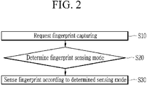
- FIG. 2 shows a flowchart for sensing a fingerprint using a fingerprint sensor according to exemplary embodiments of the present disclosure.
- the sensing controller 40 receives a fingerprint capturing request (S10).
- the sensing controller 40 determines a fingerprint sensing mode corresponding to the fingerprint capturing request (S20).
- the sensing controller 40 generates a scan control signal CONT1 and a sensing control signal CONT2 according to the determined fingerprint sensing mode, and senses the fingerprint (S30).
- the first fingerprint sensing mode will now be described with reference to FIG. 3 and FIG. 4 .
- FIG. 3 and FIG. 4 show a method for driving a fingerprint sensor in a first fingerprint sensing mode.
- the sensing driver 30 may receive sensing signals from the sensor pixels in one row.
- the sensing driver 30 receives noise signals (R[1][1]-R[1][n]) that are input by the first-row sensor pixels (SP) through the sensing lines (R1-Rn) for the first period H1. Subsequently, the sensing driver 30 receives sensing signals (R[1][1]-R[1][n]) that are input by the first-row sensor pixels (SP) through the sensing lines (R1-Rn) for the second period H2.
- the respective sensing signals that are input for the second period H2 include the noise signals of the respective sensor pixels (SP).
- the sensing driver 30 receives noise signals (R[2][1]-R[2][n]) that are input by second-row sensor pixels (SP) through the sensing lines (R1-Rn) for the third period H3, and receives sensing signals (R[2][1]-R[2][n]) that are input by the second-row sensor pixels (SP) through the sensing lines (R1-Rn) for the fourth period H4.
- noise signals R[2][1]-R[2][n]
- the sensing driver 30 receives noise signals (R[3][1]-R[3][n]) that are input by third-row sensor pixels (SP) through the sensing lines (R1-Rn) for the fifth period H5, and receives sensing signals (R[3][1]-R[3][n]) that are input by the third-row sensor pixels (SP) through the sensing lines (R1-Rn) for the sixth period H6.
- the sensing controller 40 may receive the sensing signal without the noise signals.
- the sensing controller 40 may control the scan driver 20 and the sensing driver 30 to receive the sensing signals from the first-row sensor pixels (SP) for the second period H2, the sensing signal from the second-row sensor pixels (SP) for the fourth period H4, and the sensing signals from the third-row sensor pixels (SP) for the sixth period H6 without receiving the noise signals for the first period H1, the third period H3, and the fifth period H5.
- the second fingerprint sensing mode will now be described with reference to FIG. 5 and FIG. 6 .
- FIG. 5 and FIG. 6 show a method for driving a fingerprint sensor in a second fingerprint sensing mode.
- the sensing driver 30 may sequentially receive a noise signal and a sensing signal from one sensor pixel, and may sequentially receive a noise signal and a sensing signal from another sensor pixel.
- the sensing driver 30 receives a noise signal (R[i][j]) that is input by one sensor pixel (SP) provided in the i-th row and j-th column through the sensing line R1 for the first period H1.
- the sensing driver 30 receives a sensing signal (R[i][j]) that is input by the sensor pixel (SP) through the sensing line R1 for the second period H2.
- the sensing signal that is input for the second period H2 includes the noise signal of the sensor pixel (SP).
- the sensing driver 30 receives a noise signal (R[i][j+1]) that is input by one sensor pixel (SP) provided in the i-th row and (j+1)-th column through the sensing line R2 for the third period H3, and receives the sensing signal (R[i][j+1]) that is input by the sensor pixel (SP) through the sensing line R2 for the fourth period H4.
- a noise signal R[i][j+1]
- the sensing driver 30 receives the noise signal (R[i][j+2]) that is input by the sensor pixel (SP) provided in the i-th row and (j+2)-th column through the sensing line R3 for the fifth period H5, and receives the sensing signal (R[i][j+2]) that is input by the sensor pixel (SP) through the sensing line R3 for the sixth period H6.
- the sensing controller 40 may receive the sensing signals without noise signals in the second fingerprint sensing mode.
- the sensing controller 40 may receive the sensing signal from one sensor pixel (SP) provided in the i-th row and j-th column for the second period H2, the sensing signal from one sensor pixel (SP) provided in the i-th row and (j+1)-th column for the fourth period H4, and the sensing signal from one sensor pixel (SP) provided in the i-th row and (j+2)-th column for the sixth period H6 without receiving the noise signals for the first period H1, the third period H3, and the fifth period H5.
- the sensing controller 40 may receive the sensing signal from some of a plurality of sensor pixels.
- the sensing controller 40 may receive sensing signals from the sensor pixels provided in one region of the fingerprint sensing unit 10.
- the sensing controller 40 may apply driving signals to the first-row sensor pixels of the sensor pixels provided in one region to receive the sensing signals, and may apply driving signals to the second-row sensor pixels to receive the sensing signals.
- the sensing controller 40 may apply a driving signal to one sensor pixel provided in the first row and the first column of the sensor pixels provided in one region to receive the sensing signal, and may apply the driving signal to one sensor pixel provided in the first row and second column to receive the sensing signal.
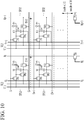
- FIG. 7 shows sensor pixels of a fingerprint sensor of FIG. 1 according to a first exemplary embodiment.
- a plurality of sensor pixels SP11, SP12, SP21, and SP22 may be disposed on the fingerprint sensing unit 10.
- the respective sensor pixels SP11, SP12, SP21, and SP22 may be connected to the corresponding initialization lines (Si, Si+1), the corresponding scan lines (Gi, Gi+1), the corresponding driving signal lines (Ej, Ej+1), the corresponding sensing lines (Rj, Rj+1), the initialization voltage line VL1, and the common voltage line VL2.
- the sensor pixel SP11 is connected to the initialization line (Si), the scan line (Gi), the driving signal line (Ej), the sensing line (Rj), the initialization voltage line VL1, and the common voltage line VL2.
- the sensor pixel SP11 includes a first transistor TR1 for initializing a first node N1, a reference capacitor (Cref) that is connected to the first node N1 and the driving signal line (Ej), a second transistor TR2 for outputting a current to the sensing line (Rj) according to a voltage at the first node N1, a third transistor TR3 for transmitting the current provided by the second transistor TR2 to the sensing line (Rj), and a touch capacitor Cf coupled in parallel to the reference capacitor (Cref) at the first node N1, of which capacitance is variable by a touch.
- the first transistor TR1 includes a first end connected to the initialization voltage line VL1, a second end connected to the first node N1, and a control end connected to the initialization line (Si).
- the second transistor TR2 includes a first end connected to the common voltage line VL2, a second end connected to a first end of the third transistor TR3, and a control end connected to the first node N1.
- the third transistor TR3 includes a first end connected to the second end of the second transistor TR2, a second end connected to the sensing line (Rj), and a control end connected to the scan line (Gi).
- the reference capacitor (Cref) includes a first end connected to the first node N1 and a second end connected to the driving signal line (Ej).
- the touch capacitor Cf includes one electrode connected to the first node N1, and changes the voltage at the first node N1 according to a user's touch.
- a plurality of switching elements may be provided outside of the fingerprint sensing unit 10.
- the switching element (TSj) is connected to the sensing line (Rj), and the switching element (TSj) includes a first end connected to the sensing line (Rj), a second end connected to the sensing driver 30 of FIG. 1 , and a control end connected to the switching line (Wj).
- the sensing line (Rj) that is connected to the first end of the switching element (TSj)
- the switching element (TSj) is turned on
- the current may be transmitted to the sensing driver 30 of FIG. 1 through the switching element (TSj).
- FIG. 8 shows a timing diagram of signals applied to sensor pixels in a first fingerprint sensing mode
- FIG. 9 to FIG. 12 show sensor pixels S11, S12, S21, and S22 operable by the signals shown in FIG. 8 .
- an initialization signal (S[i]) is supplied with an enable-level voltage for the first period H11.
- the scan signal (G[i]) is supplied with an enable-level voltage in the first period H11 in which the initialization signal (S[i]) is supplied with the enable-level voltage.
- the switching signals (W[1], ..., W[j], W[j+1], ..., W[n]) are supplied with an enable-level voltage in the first period H11 in which the scan signal (G[i]) is supplied with the enable-level voltage.
- the enable-level initialization signal (S[i]) turns on the first transistor TR1 of the sensor pixels SP11 and SP12.
- the initialization voltage (VINT) is applied to the first node N1 of the sensor pixels SP11 and SP12 through the turned-on first transistor TR1 of the sensor pixels SP11 and SP12.
- the enable-level scan signal (G[i]) turns on the third transistor TR3 of the sensor pixels SP11 and SP12, and the enable-level switching signals (W[j], W[j+1]) turn on the switching elements (TSj, TSj+1).
- Currents IN11 and IN12 may flow according to the initialization voltage (VINT) that is applied to the control end of the second transistor TR2 (or the first node N1) of the sensor pixels SP11 and SP12 and the common voltage (VCOM) that is applied to the first end of the second transistor TR2 of the sensor pixels SP11 and SP12.
- VINT initialization voltage
- VCOM common voltage
- the currents IN11 and IN12 may be transmitted to the sensing driver 30 through the respective sensing lines (Rj, Rj+1).
- the sensing driver 30 may receive the current IN11 as a noise signal of the sensor pixel SP11, and may receive the current IN12 as a noise signal of the sensor pixel SP12.
- the currents IN11 and IN12 may have different values depending on a threshold voltage (Vth) value that is unique to the second transistor TR2 included in the respective sensor pixels SP11 and SP12.
- Vth threshold voltage
- the initialization signal (S[i]) is supplied with a disable-level voltage for the second period H12.
- the scan signal (G[i]) and the driving signal (E[1], ..., E[j], E[j+1], ..., E[n]) are supplied with enable-level voltages in the second period H12 in which the initialization signal (S[i]) is supplied with a disable-level voltage.
- the switching signals (W[1], ..., W[j], W[j+1], ..., W[n]) are supplied with an enable-level voltage in the second period H12 in which the scan signal (G[i]) and the driving signals (E[1], ..., E[j], E[j+1], ..., E[n]) are supplied with the enable-level voltages.
- the enable-level driving signals (E[j], E[j+1]) are then applied to a first end of the reference capacitor (Cref) of the sensor pixels SP11 and SP12, so the voltage at the first node N1 of the sensor pixels SP11 and SP12 becomes lower than in the first period H11 by a boosting effect of the reference capacitor (Cref).
- the voltage at the first node N1 may be divided to the touch capacitor Cf that is coupled in parallel to the reference capacitor (Cref) of the sensor pixels SP11 and SP12. Therefore, the voltage at the first node N1 when a touch is provided is greater than the voltage at the first node N1 when there is no touch.
- the fingerprint of a user includes a ridge and a valley.
- a distance between one electrode of the touch capacitor Cf and the valley when the valley is touched may be longer than a distance between one electrode of the touch capacitor Cf and the ridge when the ridge is touched. Therefore, the capacitance of the touch capacitor Cf when the valley is touched may be smaller than the capacitance of the touch capacitor Cf when the ridge is touched.
- the enable-level driving signals (E[j], E[j+1]) are applied to the first end of the reference capacitor (Cref), and the voltage at the first node N1 may have values in an increasing order of when there is no touch, when the valley is touched, and when the ridge is touched.
- the scan signal (G[i]) turns on the third transistor TR3 of the sensor pixels SP11 and SP12, and the enable-level switching signals (W[j], W[j+1]) turn on the switching elements (TSj, TSj+1).
- the currents ID11 and ID12 may flow according to the voltage at the control end of the second transistor TR2 (or at the first node N1) and the common voltage (VCOM) applied to the first end of the second transistor TR2.
- the currents ID11 and ID12 may be transmitted to the sensing driver 30 through the respective sensing lines (Rj, Rj+1).
- the currents ID11 and ID12 may have values in a decreasing order of when there is no touch, when the valley is touched, and when the ridge is touched. Further, when the sensor pixels SP11 and SP12 are not touched, the currents ID11 and ID12 may have different values depending on the threshold voltage (Vth) that is unique to the second transistor TR2 included in the sensor pixels SP11 and SP12. This is identically applicable to a case when the ridge is touched or a case when the valley is touched.
- Vth threshold voltage
- the sensing driver 30 may receive the current ID11 as a sensing signal of the sensor pixel SP11, and may receive the current ID12 as a sensing signal of the sensor pixel SP12.
- the sensing driver 30 may include a subtractor (not shown) for subtracting the noise signal that is input for the first period H11 from the sensing signal that is input for the second period H12.
- the sensing driver 30 may output the sensing signal from which the noise signal is removed to the sensing controller 40 as sensing data.
- the sensing controller 40 may determine a touching state and a ridge or valley's touching state by using the sensing data.
- the sensing driver 30 may output the noise signal or the sensing signal input for respective periods to the sensing controller 40 as sensing data, and the sensing controller 40 may perform an operation for subtracting the noise signal from the sensing signal that is included in the sensing data to determine the touching state and a ridge or valley's touching state.
- the sensing controller 40 may output the sensing data to an external application processor, and the application processor may perform an operation using the sensing data, and may determine the touching state and a ridge or valley's touching state.
- the fingerprint sensor may receive the noise signal and the sensing signal from the sensor pixels SP11 and SP12 in the i-th row in the first period H11 and the second period H12, respective.
- the finger print sensor may further receive the noise signal and the sensing signal from the sensor pixels SP21 and SP22 in the (i+1)th row in the third period H13 and the fourth period H14, respectively.
- An operation of the sensor pixels SP21 and SP22 in the (i+1)th row shown in FIG. 11 and FIG. 12 is similar to an operation of the sensor pixels SP11 and SP12 in the i-th row shown in FIG. 9 and FIG. 10 , and no detailed description thereof will be provided.
- FIG. 13 shows a timing diagram of signals applied to sensor pixels in a second fingerprint sensing mode.
- the initialization signal (S[i]) is supplied with an enable-level voltage for a first period H21.
- the scan signal (G[i]) is supplied with an enable-level voltage in the first period H21 in which the initialization signal (S[i]) is supplied with the enable-level voltage.
- the switching signal (W[j]) is supplied with an enable-level voltage in the first period H21 in which the scan signal (G[i]) is supplied with the enable-level voltage.
- the enable-level initialization signal (S[i]) turns on the first transistor TR1 of the sensor pixels SP11 and SP12.
- An initialization voltage (VINT) is applied to the first node N1 of the sensor pixels SP11 and SP12 through the turned-on first transistor TR1 of the sensor pixels SP11 and SP12.
- the enable-level scan signal (G[i]) turns on the third transistor TR3 of the sensor pixels SP11 and SP12, and the enable-level switching signal (W[j]) turns on the switching element (TSj).
- the current IN11 may flow according to the initialization voltage (VINT) that is applied to the control end of the second transistor TR2 (or the first node N1) of the sensor pixel SP11 and the common voltage (VCOM) that is applied to the first end of the second transistor TR2 of the sensor pixel SP11.
- VINT initialization voltage
- VCOM common voltage
- the current IN11 may be transmitted to the sensing driver 30 through the sensing line (Rj).
- the sensing driver 30 may receive the current IN11 as a noise signal of the sensor pixel SP11.
- the initialization signal (S[i]) is supplied with a disable-level voltage for a second period H22.
- the scan signal (G[i]) and the driving signal (E[j]) are supplied with an enable-level voltage in the second period H22 in which the initialization signal (S[i]) is supplied with the disable-level voltage.
- the switching signal (W[j]) is supplied with an enable-level voltage in the second period H22 in which the scan signal (G[i]) and the driving signal (E[j]) are supplied with the enable-level voltages.
- the enable-level driving signal (E[j]) is applied to the first end of the reference capacitor (Cref) of the sensor pixel SP11, so the voltage at the first node N1 of the sensor pixel SP11 becomes lower than that of the first period H21 according to the boosting effect of the reference capacitor (Cref).
- the voltage at the first node N1 may be divided to the touch capacitor Cf that is coupled in parallel to the reference capacitor (Cref) of the sensor pixel SP11. Therefore, the voltage at the first node N1 when there is a touch is greater than the voltage at the first node N1 when there is no touch.
- the scan signal (G[i]) turns on the third transistor TR3 of the sensor pixel SP11, and the enable-level switching signal (W[j]) turns on the switching element (TSj).
- the current ID11 may then flow according to the voltage at the control end of the second transistor TR2 (or the first node N1) of the sensor pixel SP11 and the common voltage (VCOM) that is applied to the first end of the second transistor TR2.
- the current ID11 may be transmitted to the sensing driver 30 through the sensing line (Rj).
- the initialization signal (S[i]) is supplied with an enable-level voltage for a third period H23.
- the scan signal (G[i]) is supplied with an enable-level voltage in the third period H23 in which the initialization signal (S[i]) is supplied with the enable-level voltage.
- the switching signal (W[j+1]) is supplies as an enable-level voltage in the third period H23 in which the scan signal (G[i]) is supplied with the enable-level voltage.
- the current IN12 may flow according to the initialization voltage (VINT) that is applied to the control end of the second transistor TR2 (or the first node N1) of the sensor pixel SP12 and the common voltage (VCOM) that is applied to the first end of the second transistor TR2 of the sensor pixel SP12.
- VINT initialization voltage
- VCOM common voltage
- the current IN12 may be transmitted to the sensing driver 30 through the sensing line (R[j+1]).
- the sensing driver 30 may receive the current IN12 as a noise signal of the sensor pixel SP12.
- the initialization signal (S[i]) is supplied with a disable-level voltage for a fourth period H24.
- the scan signal (G[i]) and the driving signal (E[j+1]) are supplied with the enable-level voltages in the fourth period H24 in which the initialization signal (S[i]) is supplied with the disable-level voltage.
- the switching signal (W[j+1]) is supplied with an enable-level voltage in the fourth period H24 in which the scan signal (G[i]) and the driving signal (E[j+1]) are supplied with the enable-level voltages.
- An enable-level driving signal (E[j+1]) is applied to the first end of the reference capacitor (Cref) of the sensor pixel SP12, so the voltage at the first node N1 of the sensor pixel SP12 becomes lower than that of the third period H23 according to the boosting effect of the reference capacitor (Cref).
- the current ID12 may flow according to the voltage at the control end of the second transistor TR2 (or the first node N1) of the sensor pixel SP12 and the common voltage (VCOM) that is applied to the first end of the second transistor TR2.
- the current ID12 may be transmitted to the sensing driver 30 through the sensing line Rj+1.
- a sensor pixel according to a second exemplary embodiment will now be described with reference to FIG. 14 .
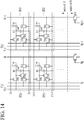
- FIG. 14 shows sensor pixels of a fingerprint sensor of FIG. 1 according to a second exemplary embodiment.
- a plurality of sensor pixels SP11, SP12, SP21, and SP22 may be disposed on the fingerprint sensing unit 10.
- the sensor pixels SP11, SP12, SP21, and SP22 shown in FIG. 14 further include a fourth transistor TR4 compared to the sensor pixel shown in FIG. 7 .
- the sensor pixel SP11 includes a first transistor TR1 for initializing a first node N1, a reference capacitor (Cref) that is connected to the first node N1 and the driving signal line (Ej), a second transistor TR2 for outputting a current to the sensing line (Rj) according to a voltage at the first node N1, a third transistor TR3 for transmitting the current provided by the second transistor TR2 to the sensing line (Rj), a fourth transistor TR4 for transmitting the common voltage (VCOM) to the second transistor TR2, and a touch capacitor Cf coupled in parallel to the reference capacitor (Cref) at the first node N1, of which capacitance changes according to a touch.
- a first transistor TR1 for initializing a first node N1
- a reference capacitor (Cref) that is connected to the first node N1 and the driving signal line (Ej)
- a second transistor TR2 for outputting a current to the sensing line (Rj) according to a voltage at the first node N1
- the first transistor TR1 includes a first end connected to the initialization voltage line VL1, a second end connected to the first node N1, and a control end connected to the initialization line (Si).
- the second transistor TR2 includes a first end connected to a second end of the fourth transistor TR4, a second end connected to the first end of the third transistor TR3, and a control end connected to the first node N1.
- the third transistor TR3 includes a first end connected to the second end of the second transistor TR2, a second end connected to the sensing line (Rj), and a control end connected to the scan line (Gi).
- the fourth transistor TR4 includes a first end connected to the common voltage line VL2, the second end connected to the first end of the second transistor TR2, and a control end connected to the scan line (Gi).
- the reference capacitor (Cref) includes a first end connected to the first node N1 and a second end connected to the driving signal line (Ej).
- the touch capacitor Cf includes one electrode connected to the first node N1, and changes the voltage at the first node N1 according to a user's touch.
- a plurality of switching elements may be provided outside of the fingerprint sensing unit 10.
- the switching element (TSj) is connected to the sensing line (Rj), and the switching element (TSj) includes a first end connected to the sensing line (Rj), a second end connected to the sensing driver 30 of FIG. 1 , and a control end connected to the switching line (Wj).
- the sensing line (Rj) that is connected to the first end of the switching element (TSj)
- the switching element (TSj) is turned on, the current may be transmitted to the sensing driver 30 of FIG. 1 through the switching element (TSj).
- the method for driving a fingerprint sensor including sensor pixels of FIG. 14 is similar to the method for driving a fingerprint sensor including sensor pixels of FIG. 7 .
- each of the sensor pixels SP11, SP12, SP21, and SP22 further include the fourth transistor TR4, thereby blocking the noise input by another sensor pixel through the common voltage line VL2.
- a potential of the user touching the sensor pixel SP21 may be different from the potential of the common voltage of the fingerprint sensor or a ground voltage of the fingerprint sensor, and the potential of the user touching may also have an alternating current (AC) characteristic.
- AC alternating current
- an AC voltage may be applied to the first end of the touch capacitor Cf.
- the potential at the first node N1 of the sensor pixel SP21 may be varied depending on the AC voltage.
- the potentials at the first end and the second end of the second transistor TR2 may be changed by parasitic capacitance (Cgs, Cgd, etc.) of the second transistor TR2 of the sensor pixel SP21.
- the potential of the common voltage line VL2 may be changed by the potential at the first end of the second transistor TR2. This may influence a value of the current output by the sensor pixel SP21.
- the turned-off fourth transistor TR4 when the turned-off fourth transistor TR4 is connected between the common voltage line VL2 and the second transistor TR2, the potential of the common voltage line VL2 may be hardly influenced when the potential of the first end of the second transistor TR2 changes. Therefore, in the second period H12, when the sensor pixel SP21 is touched, the value of the current output by the sensor pixel SP21 may not be influenced.
- a fingerprint sensor according to another exemplary embodiment of the present disclosure will now be described with reference to FIG. 15 to FIG. 17 .
- FIG. 15 shows a block diagram of a fingerprint sensor according to another exemplary embodiment of the present disclosure
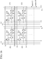
- FIG. 16 and FIG. 17 show sensor pixels of a fingerprint sensor of FIG. 15 according to various exemplary embodiments.
- the fingerprint sensor includes a fingerprint sensing unit 11, a scan driver 21, a sensing driver 31, and a sensing controller 41.
- the switching lines (W1-Wn) extend in a second direction in the fingerprint sensing unit 11, and transistors corresponding to the switching elements may be provided in the respective sensor pixels (SP).
- a plurality of sensor pixels SP11, SP12, SP21, and SP22 may be disposed on the fingerprint sensing unit 11 of FIG. 15 .
- the sensor pixel SP11 includes a first transistor TR1 for initializing a first node N1, a reference capacitor (Cref) that is connected to the first node N1 and the driving signal line (Ej), a second transistor TR2 for outputting a current to the sensing line (Rj) according to the voltage at the first node N1, a third transistor TR3 for transmitting the current provided by the second transistor TR2, a fifth transistor TR5 for transmitting the current provided by the third transistor TR3 to the sensing line (Rj), and a touch capacitor Cf coupled in parallel to the reference capacitor (Cref) at the first node N1, of which capacitance changes by a touch.
- the first transistor TR1 includes a first end connected to the initialization voltage line VL1, a second end connected to the first node N1, and a control end connected to the initialization line (Si).
- the second transistor TR2 includes a first end connected to the common voltage line VL2, a second end connected to a first end of the third transistor TR3, and a control end connected to the first node N1.
- the third transistor TR3 includes a first end connected to the second end of the second transistor TR2, a second end connected to a first end of the fifth transistor TR5, and a control end connected to the scan line (Gi).
- the fifth transistor TR5 includes the first end connected to the second end of the third transistor TR3, a second end connected to the sensing line (Rj), and a control end connected to the switching line (Wj).
- the reference capacitor (Cref) includes a first end connected to the first node N1 and a second end connected to the driving signal line (Ej).
- the touch capacitor Cf includes one electrode connected to the first node N1, and changes the voltage at the first node N1 according to a user's touch.
- the respective sensor pixels SP11, SP12, SP21, and SP22 respectively include a fifth transistor TR5 that is turned on according to a level of the switching signal.
- the method for driving a fingerprint sensor including sensor pixels of FIG. 16 is similar to the method for driving a fingerprint sensor including sensor pixels of FIG. 7 .
- An operation of the sensor pixels in a first fingerprint sensing mode will now be described with reference to FIG. 8 .
- the initialization signal (S[i]) is supplied with an enable-level voltage for the first period H11.
- the scan signal (G[i]) is supplied with an enable-level voltage in the first period H11 in which the initialization signal (S[i]) is supplied with the enable-level voltage.
- the switching signals (W[1], ..., W[j], W[j+1], ..., W[n]) are supplied with an enable-level voltage in the first period H11 in which the scan signal (G[i]) is supplied with the enable-level voltage.
- the enable-level initialization signal (S[i]) turns on the first transistor TR1 of the sensor pixels SP11 and SP12.
- the initialization voltage (VINT) is applied to the first node N1 of the sensor pixels SP11 and SP12 through the turned-on first transistor TR1 of the sensor pixels SP11 and SP12.
- the enable-level scan signal (G[i]) turns on the third transistor TR3 of the sensor pixels SP11 and SP12, and the enable-level switching signals (W[j], W[j+1]) turn on the fifth transistor TR5 of the sensor pixels SP11 and SP12.
- Currents IN11 and IN12 may flow according to the initialization voltage (VINT) that is applied to the control end N1 of the second transistor TR2 (or the first node N1) of the sensor pixels SP11 and SP12 and the common voltage (VCOM) that is applied to the first end of the second transistor TR2 of the sensor pixels SP11 and SP12.
- VINT initialization voltage
- VCOM common voltage
- the currents IN11 and IN12 may be transmitted to the sensing driver 31 of FIG. 15 through the respective sensing lines (Rj, Rj+1).
- the sensing driver 31 may receive the current IN11 as a noise signal of the sensor pixel SP11, and may receive the current IN12 as a noise signal of the sensor pixel SP12.
- the initialization signal (S[i]) is supplied with a disable-level voltage for the second period H12.
- the scan signal (G[i]) and the driving signals (E[1], ..., E[j], E[j+1], ..., E[n]) are supplied with enable-level voltages in the second period H12 in which the initialization signal (S[i]) is supplied with a disable-level voltage.
- the switching signals (W[1], ..., W[j], W[j+1], ..., W[n]) are supplied with an enable-level voltage in the second period H12 in which the scan signal (G[i]) and the driving signals (E[1], ..., E[j], E[j+1], ..., E[n]) are supplied with the enable-level voltages.
- the scan signal (G[i]) turns on the third transistor TR3 of the sensor pixels SP11 and SP12, and the enable-level switching signals (W[j], W[j+1]) turn on the fifth transistor TR5 of the sensor pixels SP11 and SP12.
- the currents ID11 and ID12 may flow according to the voltage at the control end of the second transistor TR2 (or the first node N1) and the common voltage (VCOM) that is applied to the first end of the second transistor TR2.
- the currents ID11 and ID12 may be transmitted to the sensing driver 31 through the respective sensing lines (Rj, Rj+1).
- the operation of the sensor pixels in the second fingerprint sensing mode is similar to that of the method for driving the fingerprint sensor described with reference to FIG. 13 , and no detailed description thereof will be provided.
- the sensor pixels SP11, SP12, SP21, and SP22 shown in FIG. 17 further include a fourth transistor TR4, compared to the sensor pixel shown in FIG. 16 .
- the sensor pixel SP11 includes a first transistor TR1 for initializing a first node N1, a reference capacitor (Cref) that is connected to the first node N1 and the driving signal line, a second transistor TR2 for outputting a current to the sensing line according to the voltage at the first node N1, a third transistor TR3 for transmitting the current provided by the second transistor TR2, a fourth transistor TR4 for transmitting the common voltage (VCOM) to the second transistor TR2, a fifth transistor TR5 for transmitting the current provided by the third transistor TR3 to the sensing line (Rj), and a touch capacitor Cf coupled in parallel to the reference capacitor (Cref) at the first node N1, of which capacitance changes according to a touch.
- a first transistor TR1 for initializing a first node N1, a reference capacitor (Cref) that is connected to the first node N1 and the driving signal line
- a second transistor TR2 for outputting a current to the sensing line according to the voltage at the first node N1
- the first transistor TR1 includes a first end connected to the initialization voltage line VL1, a second end connected to the first node N1, and a control end connected to the initialization line (Si).
- the second transistor TR2 includes a first end connected to a second end of the fourth transistor TR4, a second end connected to a first end of the third transistor TR3, and a control end connected to the first node N1.
- the third transistor TR3 includes the first end connected to the second end of the second transistor TR2, a second end connected to a first end of the fifth transistor TR5, and a control end connected to the scan line (Gi).
- the fourth transistor TR4 includes a first end connected to the common voltage line VL2, the second end connected to the first end of the second transistor TR2, and a control end connected to the scan line (Gi).
- the fifth transistor TR5 includes the first end connected to the second end of the third transistor TR3, a second end connected to the sensing line (Rj), and a control end connected to the switching line (Wj).
- the reference capacitor (Cref) includes a first end connected to the first node N1 and a second end connected to the driving signal line (Ej).
- the touch capacitor Cf includes one electrode connected to the first node N1, and changes the voltage at the first node N1 according to a user's touch.
- the sensor pixels SP11, SP12, SP21, and SP22 respectively include a fifth transistor TR5 that is turned on according to the level of the switching signal.
- the method for driving a fingerprint sensor including sensor pixels of FIG. 17 is similar to the method for driving a fingerprint sensor including sensor pixels of FIG. 16 .
- each of the sensor pixels SP11, SP12, SP21, and SP22 further includes the fourth transistor TR4, thereby blocking the noise input by another sensor pixel through the common voltage line VL2.
Landscapes
- Engineering & Computer Science (AREA)
- Human Computer Interaction (AREA)
- Physics & Mathematics (AREA)
- General Physics & Mathematics (AREA)
- Multimedia (AREA)
- Theoretical Computer Science (AREA)
- Computer Vision & Pattern Recognition (AREA)
- Image Input (AREA)
- Measurement Of The Respiration, Hearing Ability, Form, And Blood Characteristics Of Living Organisms (AREA)
- Measurement Of Length, Angles, Or The Like Using Electric Or Magnetic Means (AREA)
Abstract
Description
- The present disclosure relates to a sensor pixel, a fingerprint sensor, and a driving method thereof.
- As various terminals and wearable devices have been recently developed, various functions utilizing personal information such as finance or security are provided, and the importance of security verification increases.
- A verification technique by biometrics verifies a user by using fingerprints, irises, voice, face, and blood vessels. The biometric characteristics used for verification are unique to each person without having inconvenience in possession. In addition, there is less risk of illegal uses or imitation because the biometric characteristics are not easily changed for life.
- Particularly, a fingerprint verifying method is gradually becoming commercially available due to its convenience, security, and economic feasibility. In response to a user's direct or indirect contacts of his/her finger, a fingerprint sensor recognizes a fingerprint image of the finger and capture a fingerprint pattern from the fingerprint image.
- The above information disclosed in this Background section is only for enhancement of understanding of the background of the present disclosure, and therefore it may contain information that does not form the prior art that is already known to a person of ordinary skill in the art.
- The exemplary embodiments provide a fingerprint sensor for removing noise, and a driving method thereof.
- The exemplary embodiment provides a fingerprint sensor with a large area.
- An exemplary embodiment of the present disclosure provides a fingerprint sensor including: a plurality of scan lines; a plurality of driving signal lines; a plurality of sensing lines; a plurality of initialization lines; an initialization voltage line for supplying an initialization voltage; a common voltage line for supplying a common voltage; and a plurality of sensor pixels, wherein each of the sensor pixels includes: a reference capacitor including a first end connected to a driving signal line of the driving signal lines and a second end connected to a first node; a touch capacitor including one electrode connected to the first node, wherein capacitance of the touch capacitor changes by touching of an external object; a first transistor including a first end connected to the initialization voltage line, a second end connected to the first node, and a control end connected to an initialization line of the initialization lines; a second transistor including a first end for receiving the common voltage, a second end for outputting a current generated based on the common voltage, and a control end connected to the first node; and a third transistor including a first end connected to the second end of the second transistor, a second end connected to a sensing line of the sensing lines, and a control end connected to a scan line of the scan lines.
- The fingerprint sensor may further include: a plurality of switching lines; and a switching element including a first end connected to a sensing line of the sensing lines, a second end for transmitting the current, and a control end connected to a switching line of the switching lines.
- Each of the sensor pixels may further include: a fourth transistor including a first end connected to the common voltage line; a second end connected to the first end of the second transistor; and a control end connected to the scan line.
- The fingerprint sensor may further include: a scan driver for supplying a plurality of scan signals to the scan lines; a sensing driver for supplying a plurality of driving signals to the driving signal lines, and receiving currents that are output by the sensor pixels through the plurality of sensing lines; and a sensing controller for controlling the scan driver and the sensing driver to receive a first current from a first sensor pixel connected to a first scan line by supplying a first scan signal to the first scan line for a first period, and receive a second current from the first sensor pixel by supplying a second scan signal to the first scan line for a second period after the first period and supplying a driving signal to at least one of the driving signal lines.
- The scan driver may further supply a plurality of initialization signals to the initialization lines, and the sensing controller may supply the initialization voltage to the first sensor pixel by supplying the initialization signal to one of the initialization lines for the first period.
- The sensing controller may control the sensing driver to supply an enable-level voltage to at least one of the switching lines for the first period and the second period.
- The sensing driver may subtract the first current from the second current, and may output a resultant value to the sensing controller as sensing data.
- The sensing driver may output the first current to the sensing controller as first sensing data corresponding to a noise signal, and the second current as second sensing data, and the sensing controller may generate a value from the second sensing data by subtracting the first sensing data.
- The fingerprint sensor may further include a plurality of switching lines, wherein the sensor pixel may further include a fifth transistor including a first end connected to the second end of the third transistor, a second end connected to the sensing line, and a control end connected to a switching line of the switching lines.
- Another embodiment of the present disclosure provides a method for driving a fingerprint sensor including a plurality of scan lines, a plurality of driving signal lines, a plurality of sensing lines, a common voltage line for supplying a common voltage, and each of a plurality of sensor pixels being connected to a scan line of the scan lines, a driving signal line of the driving signal lines, a sensing line of the sensing lines, and the common voltage line, and outputting a current generated based on the common voltage to the sensing line while a scan signal is supplied from the scan line, the method for driving the fingerprint sensor including: receiving a first current from a first sensor pixel connected to the scan line by supplying a first scan signal to the scan line of the scan lines for a first period; and receiving a second current from the first sensor pixel by supplying a second scan signal to the scan line and supplying a driving signal to at least one driving signal line of the driving signal lines for a second period after the first period.
- The fingerprint sensor may further include a plurality of initialization lines connected to the sensor pixels and an initialization voltage line for supplying an initialization voltage to the sensor pixels, and the receiving of the first current may include: supplying the initialization voltage to the first sensor pixel by supplying an initialization signal to one of the initialization lines for the first period.
- The fingerprint sensor may further include a plurality of switching elements, wherein each of the switching elements includes a first end connected to a sensing line of the sensing lines, a second end connected to the sensing driver, and a control end connected to a switching line to which a switching signal from the sensing driver is applied, wherein the receiving of the first current and the receiving of the second current may further respectively include supplying an enable-level voltage to at least one of the switching lines.
- The fingerprint sensor may further include switching elements, wherein each of the switching elements includes a first end connected to the sensing line of the plurality of sensing lines, a second end connected to the sensing driver, and a control end connected to a switching line to which a switching signal from the sensing driver is applied, and the receiving of the first current and the receiving of the second current respectively include supplying an enable-level voltage to one of the switching lines.
- The method may further include, after receiving the second current, subtracting the first current from the second current and outputting a resultant current as sensing data.
- The method may further include, after receiving the first current, outputting the first current as first sensing data corresponding to a noise signal, and after receiving the second current, outputting the second current as second sensing data.
- The method may further include outputting a value from the second sensing data by subtracting the first sensing data.
- Yet another embodiment of the present disclosure provides a sensor pixel including: a reference capacitor including a first end connected to a driving signal line and a second end connected to a first node; a touch capacitor including one electrode connected to the first node, wherein capacitance of the touch capacitor changes by touching of an external object; a first transistor including a first end connected to an initialization voltage line, a second end connected to the first node, and a control end connected to an initialization line; a second transistor including a first end for receiving a common voltage, a second end for outputting a current generated based on the common voltage, and a control end connected to the first node; and a third transistor including a first end connected to the second end of the second transistor, a second end connected to a sensing line, and a control end connected to a scan line.
- The sensor pixel may further include a fourth transistor including a first end connected to a common voltage line for supplying the common voltage, a second end connected to the first end of the second transistor, and a control end connected to the scan line.
- The sensor pixel may further include a fifth transistor including a first end connected to the second end of the third transistor, a second end connected to the sensing line, and a control end connected to a switching line.
- According to the exemplary embodiments, the noise of the fingerprint pattern can be sensed. Further, the noise can be -reduced based on the sensed noise..
-
-
FIG. 1 shows a block diagram of a fingerprint sensor according to an exemplary embodiment of the present disclosure. -
FIG. 2 shows a flowchart for sensing a fingerprint using a fingerprint sensor according to exemplary embodiments of the present disclosure. -
FIG. 3 andFIG. 4 show a method for driving a fingerprint sensor in a first fingerprint sensing mode. -
FIG. 5 andFIG. 6 show a method for driving a fingerprint sensor in a second fingerprint sensing mode. -
FIG. 7 shows sensor pixels of a fingerprint sensor ofFIG. 1 according to a first exemplary embodiment. -
FIG. 8 shows a timing diagram of signals applied to sensor pixels in a first fingerprint sensing mode. -
FIG. 9 to FIG. 12 show sensor pixels operable by the signals shown inFIG. 8 . -
FIG. 13 shows a timing diagram of signals applied to sensor pixels in a second fingerprint sensing mode. -
FIG. 14 shows sensor pixels of a fingerprint sensor ofFIG. 1 according to a second exemplary embodiment. -
FIG. 15 shows a block diagram of a fingerprint sensor according to another exemplary embodiment of the present disclosure. -
FIG. 16 andFIG. 17 show sensor pixels of a fingerprint sensor ofFIG. 15 according to various exemplary embodiments. - The present disclosure will be described more fully hereinafter with reference to the accompanying drawings, in which exemplary embodiments are shown.
- Accordingly, the drawings and description are to be regarded as illustrative in nature and not restrictive, and like reference numerals designate like elements throughout the specification.
-
FIG. 1 shows a block diagram of a fingerprint sensor according to an exemplary embodiment of the present disclosure. - Referring to
FIG. 1 , the fingerprint sensor includes afingerprint sensing unit 10, ascan driver 20, asensing driver 30, and asensing controller 40. - The
fingerprint sensing unit 10 includes initialization lines (S1-Sm), scan lines (G1-Gm), driving signal lines (E1-En), sensing lines (R1-Rn), and sensor pixels (SP) connected to the initialization lines (S1-Sm), the scan lines (G1-Gm), the driving signal lines (E1-En), and the sensing lines (R1-Rn) and substantially arranged as a matrix. Although not shown inFIG. 1 , thefingerprint sensing unit 10 may further include an initialization voltage line for transmitting an initialization voltage (VINT) and a common voltage line for transmitting a common voltage, and the sensor pixels (SP) may be connected to the common voltage line and the initialization voltage line. The initialization voltage may have a voltage value that is greater than that of the common voltage. - The initialization lines (S1-Sm) and the scan lines (G1-Gm) may generally extend in a first direction (e.g., a row direction), and the driving signal lines (E1-En) and the sensing lines (R1-Rn) may extend in a second direction (e.g., a column direction) that crosses the first direction.
- Each of the sensor pixels (SP) may generate a sensing signal caused by a touch input according to a self-capacitance scheme. For example, when a driving signal is input to the sensor pixel (SP), a capacitor (not shown) of the sensor pixel (SP) is charged with a predetermined amount of charges depending on a touching state of an external object such as a finger, and a current corresponding to the stored amount of charges is output to the sensing lines (R1-Rn) as a sensing signal.
- That is, when the driving signal (input signal) is input to the sensor pixel (SP), the amount of charges stored in the capacitor in the sensor pixel (SP) is different according to the touching of the external object, and the corresponding sensing signal (an output signal) is transmitted to the
sensing driver 30 through the sensing lines (R1-Rn). The driving signals of the sensor pixels (SP) may be applied to the sensor pixel (SP) through the driving signal lines (E1-En). - The
sensing controller 40 controls thescan driver 20 and thesensing driver 30. Thesensing controller 40 may receive a fingerprint capturing request from an external application processor (not shown), or may receive a fingerprint sensing mode selection signal corresponding to the fingerprint capturing request. - For example, the fingerprint capturing request may be performed on an application processor or may be generated by a process. For example, when an online banking application is performed on the application processor, a fingerprint capturing request for verifying a user may be generated by an account reference process, an account transfer process, or a user log-in process, and the fingerprint capturing request may be transmitted to the
sensing controller 40. - The fingerprint sensing mode may be different according to the process performed on the application processor, and the fingerprint capturing request may trigger the fingerprint sensing mode. The
sensing controller 40 may receive a fingerprint capturing request and may be operable in the fingerprint sensing mode corresponding to the fingerprint capturing request. Alternatively, thesensing controller 40 may receive a fingerprint sensing mode selection signal for designating the fingerprint sensing mode corresponding to the fingerprint capturing request and may be operable in the designated fingerprint sensing mode. Thesensing controller 40 may directly receive the fingerprint capturing request. - The fingerprint capturing request may correspond to one of a plurality of fingerprint sensing modes. For example, the fingerprint sensing mode may include a first fingerprint sensing mode for simultaneously receiving sensing signals from sensor pixels in one row, a second fingerprint sensing mode for receiving a sensing signal from one sensor pixel and receiving a sensing signal from another sensor pixel, and a third fingerprint sensing mode for receiving sensing signals from some sensor pixels.
- The
sensing controller 40 generates a scan control signal CONT1 and a sensing control signal CONT2 according to the fingerprint sensing mode, and transmits the same to thescan driver 20 and thesensing driver 30, respectively. - The
scan driver 20 receives the scan control signal CONT1 from thesensing controller 40, generates a scan signal including an enable level voltage and a disable level voltage, and applies the same to the scan lines (G1-Gm). In addition, thescan driver 20 generates an initialization signal including an enable level voltage and a disable level voltage using the received scan control signal CONT1, and applies the same to the initialization lines (S1-Sm). -
FIG. 1 shows the exemplary embodiment in which thescan driver 20 generates the scan signal and the initialization signal, but the present disclosure is not limited thereto. For example, the fingerprint sensor may further include an initialization driver for generating an initialization signal while thescan driver 20 generates the scan signal. - The
sensing driver 30 receives the sensing control signal CONT2 from thesensing controller 40, generates driving signals including an enable level voltage and a disable level voltage, and applies the same to the driving signal lines (E1-En). In addition, thesensing driver 30 generates switching signals including an enable level voltage and a disable level voltage using the received sensing control signal CONT2, and applies the same to switching elements (SW1-SWn) through switching lines (W1-Wn). - The switching elements (SW1-SWn) may be provided outside of the
fingerprint sensing unit 10 and may be connected to the sensing lines (R1-Rn). For example, the switching elements (SW1-SWn) may be provided in thesensing driver 30. Each of the switching elements (SW1-SWn) may be turned on by a switching signal to transmit the sensing signal provided through the corresponding sensing lines (R1-Rn) to thesensing driver 30. - The
sensing driver 30 may generate sensing data based on the sensing signals. To generate sensing data (SDATA), thesensing driver 30 may include an integrator and an analog-digital converter (ADC). The sensing data (SDATA) may include fingerprint pattern information caused by the sensing signals generated by the sensor pixels (SP) to which the driving signals are input. The sensing data (SDATA) may be transmitted to thesensing controller 40 or an external application processor. - A method for sensing a fingerprint using the above-described fingerprint sensor according to a fingerprint sensing mode will now be described with reference to
FIG. 2 to FIG. 6 . -
FIG. 2 shows a flowchart for sensing a fingerprint using a fingerprint sensor according to exemplary embodiments of the present disclosure. Referring toFIG. 2 , thesensing controller 40 receives a fingerprint capturing request (S10). - The
sensing controller 40 determines a fingerprint sensing mode corresponding to the fingerprint capturing request (S20). Thesensing controller 40 generates a scan control signal CONT1 and a sensing control signal CONT2 according to the determined fingerprint sensing mode, and senses the fingerprint (S30). - The first fingerprint sensing mode will now be described with reference to
FIG. 3 andFIG. 4 . -
FIG. 3 andFIG. 4 show a method for driving a fingerprint sensor in a first fingerprint sensing mode. - Referring to
FIG. 3 , in the first fingerprint sensing mode, thesensing driver 30 may receive sensing signals from the sensor pixels in one row. - Referring to
FIG. 4A , thesensing driver 30 receives noise signals (R[1][1]-R[1][n]) that are input by the first-row sensor pixels (SP) through the sensing lines (R1-Rn) for the first period H1. Subsequently, thesensing driver 30 receives sensing signals (R[1][1]-R[1][n]) that are input by the first-row sensor pixels (SP) through the sensing lines (R1-Rn) for the second period H2. The respective sensing signals that are input for the second period H2 include the noise signals of the respective sensor pixels (SP). - Referring to
FIG. 4B , thesensing driver 30 receives noise signals (R[2][1]-R[2][n]) that are input by second-row sensor pixels (SP) through the sensing lines (R1-Rn) for the third period H3, and receives sensing signals (R[2][1]-R[2][n]) that are input by the second-row sensor pixels (SP) through the sensing lines (R1-Rn) for the fourth period H4. In a like manner, referring toFIG. 4C , thesensing driver 30 receives noise signals (R[3][1]-R[3][n]) that are input by third-row sensor pixels (SP) through the sensing lines (R1-Rn) for the fifth period H5, and receives sensing signals (R[3][1]-R[3][n]) that are input by the third-row sensor pixels (SP) through the sensing lines (R1-Rn) for the sixth period H6. - The
sensing controller 40 may receive the sensing signal without the noise signals. For example, thesensing controller 40 may control thescan driver 20 and thesensing driver 30 to receive the sensing signals from the first-row sensor pixels (SP) for the second period H2, the sensing signal from the second-row sensor pixels (SP) for the fourth period H4, and the sensing signals from the third-row sensor pixels (SP) for the sixth period H6 without receiving the noise signals for the first period H1, the third period H3, and the fifth period H5. - The second fingerprint sensing mode will now be described with reference to
FIG. 5 andFIG. 6 . -
FIG. 5 andFIG. 6 show a method for driving a fingerprint sensor in a second fingerprint sensing mode. - Referring to
FIG. 5 , in the second fingerprint sensing mode, thesensing driver 30 may sequentially receive a noise signal and a sensing signal from one sensor pixel, and may sequentially receive a noise signal and a sensing signal from another sensor pixel. - Referring to
FIG. 6A , thesensing driver 30 receives a noise signal (R[i][j]) that is input by one sensor pixel (SP) provided in the i-th row and j-th column through the sensing line R1 for the first period H1. Thesensing driver 30 receives a sensing signal (R[i][j]) that is input by the sensor pixel (SP) through the sensing line R1 for the second period H2. The sensing signal that is input for the second period H2 includes the noise signal of the sensor pixel (SP). - Referring to
FIG. 6B , thesensing driver 30 receives a noise signal (R[i][j+1]) that is input by one sensor pixel (SP) provided in the i-th row and (j+1)-th column through the sensing line R2 for the third period H3, and receives the sensing signal (R[i][j+1]) that is input by the sensor pixel (SP) through the sensing line R2 for the fourth period H4. In a like manner, referring toFIG. 6C , thesensing driver 30 receives the noise signal (R[i][j+2]) that is input by the sensor pixel (SP) provided in the i-th row and (j+2)-th column through the sensing line R3 for the fifth period H5, and receives the sensing signal (R[i][j+2]) that is input by the sensor pixel (SP) through the sensing line R3 for the sixth period H6. - The
sensing controller 40 may receive the sensing signals without noise signals in the second fingerprint sensing mode. For example, thesensing controller 40 may receive the sensing signal from one sensor pixel (SP) provided in the i-th row and j-th column for the second period H2, the sensing signal from one sensor pixel (SP) provided in the i-th row and (j+1)-th column for the fourth period H4, and the sensing signal from one sensor pixel (SP) provided in the i-th row and (j+2)-th column for the sixth period H6 without receiving the noise signals for the first period H1, the third period H3, and the fifth period H5. - Although not shown in the drawing, in the third fingerprint sensing mode, the
sensing controller 40 may receive the sensing signal from some of a plurality of sensor pixels. For example, thesensing controller 40 may receive sensing signals from the sensor pixels provided in one region of thefingerprint sensing unit 10. - In the third fingerprint sensing mode, in a like manner of the first fingerprint sensing mode, the
sensing controller 40 may apply driving signals to the first-row sensor pixels of the sensor pixels provided in one region to receive the sensing signals, and may apply driving signals to the second-row sensor pixels to receive the sensing signals. - In another way, in the third fingerprint sensing mode, in a like manner of the second fingerprint sensing mode, the
sensing controller 40 may apply a driving signal to one sensor pixel provided in the first row and the first column of the sensor pixels provided in one region to receive the sensing signal, and may apply the driving signal to one sensor pixel provided in the first row and second column to receive the sensing signal. - Sensor pixels according to a first exemplary embodiment will now be described with reference to
FIG. 7 . -
FIG. 7 shows sensor pixels of a fingerprint sensor ofFIG. 1 according to a first exemplary embodiment. Referring toFIG. 7 , a plurality of sensor pixels SP11, SP12, SP21, and SP22 may be disposed on thefingerprint sensing unit 10. - The respective sensor pixels SP11, SP12, SP21, and SP22 may be connected to the corresponding initialization lines (Si, Si+1), the corresponding scan lines (Gi, Gi+1), the corresponding driving signal lines (Ej, Ej+1), the corresponding sensing lines (Rj, Rj+1), the initialization voltage line VL1, and the common voltage line VL2. For example, the sensor pixel SP11 is connected to the initialization line (Si), the scan line (Gi), the driving signal line (Ej), the sensing line (Rj), the initialization voltage line VL1, and the common voltage line VL2.
- The sensor pixel SP11 includes a first transistor TR1 for initializing a first node N1, a reference capacitor (Cref) that is connected to the first node N1 and the driving signal line (Ej), a second transistor TR2 for outputting a current to the sensing line (Rj) according to a voltage at the first node N1, a third transistor TR3 for transmitting the current provided by the second transistor TR2 to the sensing line (Rj), and a touch capacitor Cf coupled in parallel to the reference capacitor (Cref) at the first node N1, of which capacitance is variable by a touch.
- The first transistor TR1 includes a first end connected to the initialization voltage line VL1, a second end connected to the first node N1, and a control end connected to the initialization line (Si).
- The second transistor TR2 includes a first end connected to the common voltage line VL2, a second end connected to a first end of the third transistor TR3, and a control end connected to the first node N1.
- The third transistor TR3 includes a first end connected to the second end of the second transistor TR2, a second end connected to the sensing line (Rj), and a control end connected to the scan line (Gi).
- The reference capacitor (Cref) includes a first end connected to the first node N1 and a second end connected to the driving signal line (Ej).
- The touch capacitor Cf includes one electrode connected to the first node N1, and changes the voltage at the first node N1 according to a user's touch.
- A plurality of switching elements (TSj, TSj+1) may be provided outside of the
fingerprint sensing unit 10. For example, the switching element (TSj) is connected to the sensing line (Rj), and the switching element (TSj) includes a first end connected to the sensing line (Rj), a second end connected to thesensing driver 30 ofFIG. 1 , and a control end connected to the switching line (Wj). When current flows through the sensing line (Rj) that is connected to the first end of the switching element (TSj), and the switching element (TSj) is turned on, the current may be transmitted to thesensing driver 30 ofFIG. 1 through the switching element (TSj). - An operation of sensor pixels in a first fingerprint sensing mode will now be described with reference to
FIG. 8 to FIG. 12 . -
FIG. 8 shows a timing diagram of signals applied to sensor pixels in a first fingerprint sensing mode, andFIG. 9 to FIG. 12 show sensor pixels S11, S12, S21, and S22 operable by the signals shown inFIG. 8 . - Referring to
FIG. 8 andFIG. 9 , an initialization signal (S[i]) is supplied with an enable-level voltage for the first period H11. The scan signal (G[i]) is supplied with an enable-level voltage in the first period H11 in which the initialization signal (S[i]) is supplied with the enable-level voltage. Further, the switching signals (W[1], ..., W[j], W[j+1], ..., W[n]) are supplied with an enable-level voltage in the first period H11 in which the scan signal (G[i]) is supplied with the enable-level voltage. - The enable-level initialization signal (S[i]) turns on the first transistor TR1 of the sensor pixels SP11 and SP12. The initialization voltage (VINT) is applied to the first node N1 of the sensor pixels SP11 and SP12 through the turned-on first transistor TR1 of the sensor pixels SP11 and SP12. The enable-level scan signal (G[i]) turns on the third transistor TR3 of the sensor pixels SP11 and SP12, and the enable-level switching signals (W[j], W[j+1]) turn on the switching elements (TSj, TSj+1).
- Currents IN11 and IN12 may flow according to the initialization voltage (VINT) that is applied to the control end of the second transistor TR2 (or the first node N1) of the sensor pixels SP11 and SP12 and the common voltage (VCOM) that is applied to the first end of the second transistor TR2 of the sensor pixels SP11 and SP12. The currents IN11 and IN12 may be transmitted to the
sensing driver 30 through the respective sensing lines (Rj, Rj+1). Thesensing driver 30 may receive the current IN11 as a noise signal of the sensor pixel SP11, and may receive the current IN12 as a noise signal of the sensor pixel SP12. - The currents IN11 and IN12 may have different values depending on a threshold voltage (Vth) value that is unique to the second transistor TR2 included in the respective sensor pixels SP11 and SP12.
- Referring to
FIG. 8 andFIG. 10 , the initialization signal (S[i]) is supplied with a disable-level voltage for the second period H12. The scan signal (G[i]) and the driving signal (E[1], ..., E[j], E[j+1], ..., E[n]) are supplied with enable-level voltages in the second period H12 in which the initialization signal (S[i]) is supplied with a disable-level voltage. Further, the switching signals (W[1], ..., W[j], W[j+1], ..., W[n]) are supplied with an enable-level voltage in the second period H12 in which the scan signal (G[i]) and the driving signals (E[1], ..., E[j], E[j+1], ..., E[n]) are supplied with the enable-level voltages. - The enable-level driving signals (E[j], E[j+1]) are then applied to a first end of the reference capacitor (Cref) of the sensor pixels SP11 and SP12, so the voltage at the first node N1 of the sensor pixels SP11 and SP12 becomes lower than in the first period H11 by a boosting effect of the reference capacitor (Cref).
- In this instance, when there is a touch on the sensor pixels SP11 and SP12, the voltage at the first node N1 may be divided to the touch capacitor Cf that is coupled in parallel to the reference capacitor (Cref) of the sensor pixels SP11 and SP12. Therefore, the voltage at the first node N1 when a touch is provided is greater than the voltage at the first node N1 when there is no touch.
- Further, the fingerprint of a user includes a ridge and a valley. A distance between one electrode of the touch capacitor Cf and the valley when the valley is touched may be longer than a distance between one electrode of the touch capacitor Cf and the ridge when the ridge is touched. Therefore, the capacitance of the touch capacitor Cf when the valley is touched may be smaller than the capacitance of the touch capacitor Cf when the ridge is touched.
- In summary, the enable-level driving signals (E[j], E[j+1]) are applied to the first end of the reference capacitor (Cref), and the voltage at the first node N1 may have values in an increasing order of when there is no touch, when the valley is touched, and when the ridge is touched.
- The scan signal (G[i]) turns on the third transistor TR3 of the sensor pixels SP11 and SP12, and the enable-level switching signals (W[j], W[j+1]) turn on the switching elements (TSj, TSj+1).
- The currents ID11 and ID12 may flow according to the voltage at the control end of the second transistor TR2 (or at the first node N1) and the common voltage (VCOM) applied to the first end of the second transistor TR2. The currents ID11 and ID12 may be transmitted to the
sensing driver 30 through the respective sensing lines (Rj, Rj+1). - The currents ID11 and ID12 may have values in a decreasing order of when there is no touch, when the valley is touched, and when the ridge is touched. Further, when the sensor pixels SP11 and SP12 are not touched, the currents ID11 and ID12 may have different values depending on the threshold voltage (Vth) that is unique to the second transistor TR2 included in the sensor pixels SP11 and SP12. This is identically applicable to a case when the ridge is touched or a case when the valley is touched.
- The
sensing driver 30 may receive the current ID11 as a sensing signal of the sensor pixel SP11, and may receive the current ID12 as a sensing signal of the sensor pixel SP12. - According to one embodiment, the
sensing driver 30 may include a subtractor (not shown) for subtracting the noise signal that is input for the first period H11 from the sensing signal that is input for the second period H12. Thesensing driver 30 may output the sensing signal from which the noise signal is removed to thesensing controller 40 as sensing data. Thesensing controller 40 may determine a touching state and a ridge or valley's touching state by using the sensing data. - In another embodiment, the
sensing driver 30 may output the noise signal or the sensing signal input for respective periods to thesensing controller 40 as sensing data, and thesensing controller 40 may perform an operation for subtracting the noise signal from the sensing signal that is included in the sensing data to determine the touching state and a ridge or valley's touching state. - In addition, the
sensing controller 40 may output the sensing data to an external application processor, and the application processor may perform an operation using the sensing data, and may determine the touching state and a ridge or valley's touching state. - The fingerprint sensor may receive the noise signal and the sensing signal from the sensor pixels SP11 and SP12 in the i-th row in the first period H11 and the second period H12, respective. In a like manner, the finger print sensor may further receive the noise signal and the sensing signal from the sensor pixels SP21 and SP22 in the (i+1)th row in the third period H13 and the fourth period H14, respectively.
- An operation of the sensor pixels SP21 and SP22 in the (i+1)th row shown in
FIG. 11 andFIG. 12 is similar to an operation of the sensor pixels SP11 and SP12 in the i-th row shown inFIG. 9 andFIG. 10 , and no detailed description thereof will be provided. - An operation of the sensor pixels in a second fingerprint sensing mode will now be described with reference to
FIG. 7 andFIG. 13 . -
FIG. 13 shows a timing diagram of signals applied to sensor pixels in a second fingerprint sensing mode. - Referring to
FIG. 13 , the initialization signal (S[i]) is supplied with an enable-level voltage for a first period H21. The scan signal (G[i]) is supplied with an enable-level voltage in the first period H21 in which the initialization signal (S[i]) is supplied with the enable-level voltage. Further, the switching signal (W[j]) is supplied with an enable-level voltage in the first period H21 in which the scan signal (G[i]) is supplied with the enable-level voltage. - The enable-level initialization signal (S[i]) turns on the first transistor TR1 of the sensor pixels SP11 and SP12. An initialization voltage (VINT) is applied to the first node N1 of the sensor pixels SP11 and SP12 through the turned-on first transistor TR1 of the sensor pixels SP11 and SP12. The enable-level scan signal (G[i]) turns on the third transistor TR3 of the sensor pixels SP11 and SP12, and the enable-level switching signal (W[j]) turns on the switching element (TSj).
- The current IN11 may flow according to the initialization voltage (VINT) that is applied to the control end of the second transistor TR2 (or the first node N1) of the sensor pixel SP11 and the common voltage (VCOM) that is applied to the first end of the second transistor TR2 of the sensor pixel SP11. The current IN11 may be transmitted to the
sensing driver 30 through the sensing line (Rj). Thesensing driver 30 may receive the current IN11 as a noise signal of the sensor pixel SP11. - The initialization signal (S[i]) is supplied with a disable-level voltage for a second period H22. The scan signal (G[i]) and the driving signal (E[j]) are supplied with an enable-level voltage in the second period H22 in which the initialization signal (S[i]) is supplied with the disable-level voltage. Further, the switching signal (W[j]) is supplied with an enable-level voltage in the second period H22 in which the scan signal (G[i]) and the driving signal (E[j]) are supplied with the enable-level voltages.
- The enable-level driving signal (E[j]) is applied to the first end of the reference capacitor (Cref) of the sensor pixel SP11, so the voltage at the first node N1 of the sensor pixel SP11 becomes lower than that of the first period H21 according to the boosting effect of the reference capacitor (Cref).
- In this instance, when the sensor pixel SP11 is touched, the voltage at the first node N1 may be divided to the touch capacitor Cf that is coupled in parallel to the reference capacitor (Cref) of the sensor pixel SP11. Therefore, the voltage at the first node N1 when there is a touch is greater than the voltage at the first node N1 when there is no touch.
- The scan signal (G[i]) turns on the third transistor TR3 of the sensor pixel SP11, and the enable-level switching signal (W[j]) turns on the switching element (TSj).
- The current ID11 may then flow according to the voltage at the control end of the second transistor TR2 (or the first node N1) of the sensor pixel SP11 and the common voltage (VCOM) that is applied to the first end of the second transistor TR2. The current ID11 may be transmitted to the
sensing driver 30 through the sensing line (Rj). - The initialization signal (S[i]) is supplied with an enable-level voltage for a third period H23. The scan signal (G[i]) is supplied with an enable-level voltage in the third period H23 in which the initialization signal (S[i]) is supplied with the enable-level voltage. Further, the switching signal (W[j+1]) is supplies as an enable-level voltage in the third period H23 in which the scan signal (G[i]) is supplied with the enable-level voltage.
- The current IN12 may flow according to the initialization voltage (VINT) that is applied to the control end of the second transistor TR2 (or the first node N1) of the sensor pixel SP12 and the common voltage (VCOM) that is applied to the first end of the second transistor TR2 of the sensor pixel SP12. The current IN12 may be transmitted to the
sensing driver 30 through the sensing line (R[j+1]). Thesensing driver 30 may receive the current IN12 as a noise signal of the sensor pixel SP12. - The initialization signal (S[i]) is supplied with a disable-level voltage for a fourth period H24. The scan signal (G[i]) and the driving signal (E[j+1]) are supplied with the enable-level voltages in the fourth period H24 in which the initialization signal (S[i]) is supplied with the disable-level voltage. Further, the switching signal (W[j+1]) is supplied with an enable-level voltage in the fourth period H24 in which the scan signal (G[i]) and the driving signal (E[j+1]) are supplied with the enable-level voltages.
- An enable-level driving signal (E[j+1]) is applied to the first end of the reference capacitor (Cref) of the sensor pixel SP12, so the voltage at the first node N1 of the sensor pixel SP12 becomes lower than that of the third period H23 according to the boosting effect of the reference capacitor (Cref).
- The current ID12 may flow according to the voltage at the control end of the second transistor TR2 (or the first node N1) of the sensor pixel SP12 and the common voltage (VCOM) that is applied to the first end of the second transistor TR2. The current ID12 may be transmitted to the
sensing driver 30 through the sensingline Rj+ 1. - A sensor pixel according to a second exemplary embodiment will now be described with reference to
FIG. 14 . -
FIG. 14 shows sensor pixels of a fingerprint sensor ofFIG. 1 according to a second exemplary embodiment. - Referring to
FIG. 14 , a plurality of sensor pixels SP11, SP12, SP21, and SP22 may be disposed on thefingerprint sensing unit 10. The sensor pixels SP11, SP12, SP21, and SP22 shown inFIG. 14 further include a fourth transistor TR4 compared to the sensor pixel shown inFIG. 7 . - The sensor pixel SP11 includes a first transistor TR1 for initializing a first node N1, a reference capacitor (Cref) that is connected to the first node N1 and the driving signal line (Ej), a second transistor TR2 for outputting a current to the sensing line (Rj) according to a voltage at the first node N1, a third transistor TR3 for transmitting the current provided by the second transistor TR2 to the sensing line (Rj), a fourth transistor TR4 for transmitting the common voltage (VCOM) to the second transistor TR2, and a touch capacitor Cf coupled in parallel to the reference capacitor (Cref) at the first node N1, of which capacitance changes according to a touch.
- The first transistor TR1 includes a first end connected to the initialization voltage line VL1, a second end connected to the first node N1, and a control end connected to the initialization line (Si).
- The second transistor TR2 includes a first end connected to a second end of the fourth transistor TR4, a second end connected to the first end of the third transistor TR3, and a control end connected to the first node N1.
- The third transistor TR3 includes a first end connected to the second end of the second transistor TR2, a second end connected to the sensing line (Rj), and a control end connected to the scan line (Gi).
- The fourth transistor TR4 includes a first end connected to the common voltage line VL2, the second end connected to the first end of the second transistor TR2, and a control end connected to the scan line (Gi).
- The reference capacitor (Cref) includes a first end connected to the first node N1 and a second end connected to the driving signal line (Ej).
- The touch capacitor Cf includes one electrode connected to the first node N1, and changes the voltage at the first node N1 according to a user's touch.
- In a like manner of the sensor pixel of
FIG. 7 , a plurality of switching elements (TSj, TSj+1) may be provided outside of thefingerprint sensing unit 10. For example, the switching element (TSj) is connected to the sensing line (Rj), and the switching element (TSj) includes a first end connected to the sensing line (Rj), a second end connected to thesensing driver 30 ofFIG. 1 , and a control end connected to the switching line (Wj). When current flows through the sensing line (Rj) that is connected to the first end of the switching element (TSj), and the switching element (TSj) is turned on, the current may be transmitted to thesensing driver 30 ofFIG. 1 through the switching element (TSj). - The method for driving a fingerprint sensor including sensor pixels of
FIG. 14 is similar to the method for driving a fingerprint sensor including sensor pixels ofFIG. 7 . However, each of the sensor pixels SP11, SP12, SP21, and SP22 further include the fourth transistor TR4, thereby blocking the noise input by another sensor pixel through the common voltage line VL2. - A case in which the sensor pixel SP11 is not touched and the sensor pixel SP21 is touched in the second period H12 of
FIG. 8 will now be described. - A potential of the user touching the sensor pixel SP21 may be different from the potential of the common voltage of the fingerprint sensor or a ground voltage of the fingerprint sensor, and the potential of the user touching may also have an alternating current (AC) characteristic.
- Therefore, when the user's finger touches the touch capacitor Cf of the sensor pixel SP21, an AC voltage may be applied to the first end of the touch capacitor Cf. The potential at the first node N1 of the sensor pixel SP21 may be varied depending on the AC voltage. When the potential of the first node N1 changes, the potentials at the first end and the second end of the second transistor TR2 may be changed by parasitic capacitance (Cgs, Cgd, etc.) of the second transistor TR2 of the sensor pixel SP21.
- When the fourth transistor TR4 is not connected between the common voltage line VL2 and the second transistor TR2, the potential of the common voltage line VL2 may be changed by the potential at the first end of the second transistor TR2. This may influence a value of the current output by the sensor pixel SP21.
- However, when the turned-off fourth transistor TR4 is connected between the common voltage line VL2 and the second transistor TR2, the potential of the common voltage line VL2 may be hardly influenced when the potential of the first end of the second transistor TR2 changes. Therefore, in the second period H12, when the sensor pixel SP21 is touched, the value of the current output by the sensor pixel SP21 may not be influenced.
- A fingerprint sensor according to another exemplary embodiment of the present disclosure will now be described with reference to
FIG. 15 to FIG. 17 . -
FIG. 15 shows a block diagram of a fingerprint sensor according to another exemplary embodiment of the present disclosure, andFIG. 16 andFIG. 17 show sensor pixels of a fingerprint sensor ofFIG. 15 according to various exemplary embodiments. - Referring to
FIG. 15 , the fingerprint sensor includes afingerprint sensing unit 11, ascan driver 21, asensing driver 31, and asensing controller 41. - Regarding the fingerprint sensor shown in
FIG. 15 , compared to the fingerprint sensor shown inFIG. 1 , the switching lines (W1-Wn) extend in a second direction in thefingerprint sensing unit 11, and transistors corresponding to the switching elements may be provided in the respective sensor pixels (SP). - Referring to
FIG. 16 andFIG. 17 , a plurality of sensor pixels SP11, SP12, SP21, and SP22 may be disposed on thefingerprint sensing unit 11 ofFIG. 15 . - The sensor pixel SP11 includes a first transistor TR1 for initializing a first node N1, a reference capacitor (Cref) that is connected to the first node N1 and the driving signal line (Ej), a second transistor TR2 for outputting a current to the sensing line (Rj) according to the voltage at the first node N1, a third transistor TR3 for transmitting the current provided by the second transistor TR2, a fifth transistor TR5 for transmitting the current provided by the third transistor TR3 to the sensing line (Rj), and a touch capacitor Cf coupled in parallel to the reference capacitor (Cref) at the first node N1, of which capacitance changes by a touch.
- The first transistor TR1 includes a first end connected to the initialization voltage line VL1, a second end connected to the first node N1, and a control end connected to the initialization line (Si).
- The second transistor TR2 includes a first end connected to the common voltage line VL2, a second end connected to a first end of the third transistor TR3, and a control end connected to the first node N1.
- The third transistor TR3 includes a first end connected to the second end of the second transistor TR2, a second end connected to a first end of the fifth transistor TR5, and a control end connected to the scan line (Gi).
- The fifth transistor TR5 includes the first end connected to the second end of the third transistor TR3, a second end connected to the sensing line (Rj), and a control end connected to the switching line (Wj).
- The reference capacitor (Cref) includes a first end connected to the first node N1 and a second end connected to the driving signal line (Ej).
- The touch capacitor Cf includes one electrode connected to the first node N1, and changes the voltage at the first node N1 according to a user's touch.
- The respective sensor pixels SP11, SP12, SP21, and SP22 respectively include a fifth transistor TR5 that is turned on according to a level of the switching signal.
- The method for driving a fingerprint sensor including sensor pixels of
FIG. 16 is similar to the method for driving a fingerprint sensor including sensor pixels ofFIG. 7 . An operation of the sensor pixels in a first fingerprint sensing mode will now be described with reference toFIG. 8 . - The initialization signal (S[i]) is supplied with an enable-level voltage for the first period H11. The scan signal (G[i]) is supplied with an enable-level voltage in the first period H11 in which the initialization signal (S[i]) is supplied with the enable-level voltage. Further, the switching signals (W[1], ..., W[j], W[j+1], ..., W[n]) are supplied with an enable-level voltage in the first period H11 in which the scan signal (G[i]) is supplied with the enable-level voltage.
- The enable-level initialization signal (S[i]) turns on the first transistor TR1 of the sensor pixels SP11 and SP12. The initialization voltage (VINT) is applied to the first node N1 of the sensor pixels SP11 and SP12 through the turned-on first transistor TR1 of the sensor pixels SP11 and SP12. The enable-level scan signal (G[i]) turns on the third transistor TR3 of the sensor pixels SP11 and SP12, and the enable-level switching signals (W[j], W[j+1]) turn on the fifth transistor TR5 of the sensor pixels SP11 and SP12.
- Currents IN11 and IN12 may flow according to the initialization voltage (VINT) that is applied to the control end N1 of the second transistor TR2 (or the first node N1) of the sensor pixels SP11 and SP12 and the common voltage (VCOM) that is applied to the first end of the second transistor TR2 of the sensor pixels SP11 and SP12. The currents IN11 and IN12 may be transmitted to the
sensing driver 31 ofFIG. 15 through the respective sensing lines (Rj, Rj+1). Thesensing driver 31 may receive the current IN11 as a noise signal of the sensor pixel SP11, and may receive the current IN12 as a noise signal of the sensor pixel SP12. - The initialization signal (S[i]) is supplied with a disable-level voltage for the second period H12. The scan signal (G[i]) and the driving signals (E[1], ..., E[j], E[j+1], ..., E[n]) are supplied with enable-level voltages in the second period H12 in which the initialization signal (S[i]) is supplied with a disable-level voltage. Further, the switching signals (W[1], ..., W[j], W[j+1], ..., W[n]) are supplied with an enable-level voltage in the second period H12 in which the scan signal (G[i]) and the driving signals (E[1], ..., E[j], E[j+1], ..., E[n]) are supplied with the enable-level voltages.
- The scan signal (G[i]) turns on the third transistor TR3 of the sensor pixels SP11 and SP12, and the enable-level switching signals (W[j], W[j+1]) turn on the fifth transistor TR5 of the sensor pixels SP11 and SP12.
- The currents ID11 and ID12 may flow according to the voltage at the control end of the second transistor TR2 (or the first node N1) and the common voltage (VCOM) that is applied to the first end of the second transistor TR2. The currents ID11 and ID12 may be transmitted to the
sensing driver 31 through the respective sensing lines (Rj, Rj+1). - The operation of the sensor pixels in the second fingerprint sensing mode is similar to that of the method for driving the fingerprint sensor described with reference to
FIG. 13 , and no detailed description thereof will be provided. - The sensor pixels SP11, SP12, SP21, and SP22 shown in
FIG. 17 further include a fourth transistor TR4, compared to the sensor pixel shown inFIG. 16 . - The sensor pixel SP11 includes a first transistor TR1 for initializing a first node N1, a reference capacitor (Cref) that is connected to the first node N1 and the driving signal line, a second transistor TR2 for outputting a current to the sensing line according to the voltage at the first node N1, a third transistor TR3 for transmitting the current provided by the second transistor TR2, a fourth transistor TR4 for transmitting the common voltage (VCOM) to the second transistor TR2, a fifth transistor TR5 for transmitting the current provided by the third transistor TR3 to the sensing line (Rj), and a touch capacitor Cf coupled in parallel to the reference capacitor (Cref) at the first node N1, of which capacitance changes according to a touch.
- The first transistor TR1 includes a first end connected to the initialization voltage line VL1, a second end connected to the first node N1, and a control end connected to the initialization line (Si).
- The second transistor TR2 includes a first end connected to a second end of the fourth transistor TR4, a second end connected to a first end of the third transistor TR3, and a control end connected to the first node N1.
- The third transistor TR3 includes the first end connected to the second end of the second transistor TR2, a second end connected to a first end of the fifth transistor TR5, and a control end connected to the scan line (Gi).
- The fourth transistor TR4 includes a first end connected to the common voltage line VL2, the second end connected to the first end of the second transistor TR2, and a control end connected to the scan line (Gi).
- The fifth transistor TR5 includes the first end connected to the second end of the third transistor TR3, a second end connected to the sensing line (Rj), and a control end connected to the switching line (Wj).
- The reference capacitor (Cref) includes a first end connected to the first node N1 and a second end connected to the driving signal line (Ej).
- The touch capacitor Cf includes one electrode connected to the first node N1, and changes the voltage at the first node N1 according to a user's touch.
- The sensor pixels SP11, SP12, SP21, and SP22 respectively include a fifth transistor TR5 that is turned on according to the level of the switching signal.
- The method for driving a fingerprint sensor including sensor pixels of
FIG. 17 is similar to the method for driving a fingerprint sensor including sensor pixels ofFIG. 16 . However, each of the sensor pixels SP11, SP12, SP21, and SP22 further includes the fourth transistor TR4, thereby blocking the noise input by another sensor pixel through the common voltage line VL2. - It is clear for a person skilled in the art that the disclosed embodiments can also be combined where possible.
Claims (15)
- A fingerprint sensor comprising:a plurality of scan lines (G1-Gm); a plurality of driving signal lines (E1-En); a plurality of sensing lines (R1-Rn); a plurality of initialization lines (S1-Sm); an initialization voltage line (VL1) for supplying an initialization voltage; a common voltage line (VL2) for supplying a common voltage; and a plurality of sensor pixels (SP),wherein each of the sensor pixels (SP) includes:a reference capacitor (Cref) including a first end connected to a driving signal line (Ej) of the driving signal lines (E1-En) and a second end connected to a first node (N1);a touch capacitor (Cf) including one electrode connected to the first node (N1), wherein capacitance of the touch capacitor changes by touching of an external object;a first transistor (TR1) including a first end connected to the initialization voltage line, a second end connected to the first node (N1), and a control end connected to an initialization line (Si) of the initialization lines;a second transistor (TR2) including a first end for receiving the common voltage, a second end for outputting a current generated based on the common voltage, and a control end connected to the first node (N1); anda third transistor (TR3) including a first end connected to the second end of the second transistor (TR2), a second end connected to a sensing line (Rj) of the sensing lines (R1-Rn), and a control end connected to a scan line (Gi) of the scan lines (G1-Gm).
- The fingerprint sensor of claim 1, further comprising:a plurality of switching lines (W1-Wn); anda switching element (TSj) including a first end connected to a sensing line (Rj) of the sensing lines (R1-Rn), a second end for transmitting the current, and a control end connected to a switching line (Wj) of the switching lines (W1-Wn).
- The fingerprint sensor of claim 1 or 2, wherein
each of the sensor pixels (SP) further includes: a fourth transistor (TR4) including a first end connected to the common voltage line; a second end connected to the first end of the second transistor (TR2); and a control end connected to the scan line (G1-Gm). - The fingerprint sensor of one of the preceding claims , further comprising:a scan driver (20) for supplying a plurality of scan signals to the scan lines (G1-Gm);a sensing driver (30) for supplying a plurality of driving signals to the driving signal lines (E1-En), and receiving currents that are output by the sensor pixels through the plurality of sensing lines (R1-Rn); anda sensing controller (40) for controlling the scan driver (20) and the sensing driver (30) to receive a first current from a first sensor pixel (SP11) connected to a first scan line (Gi) by supplying a first scan signal to the first scan line (Gi) for a first period, and receive a second current from the first sensor pixel (SP11) by supplying a second scan signal to the first scan line (Gi) for a second period after the first period and supplying a driving signal to at least one of the driving signal lines (Ej).
- The fingerprint sensor of claim 4, wherein
the scan driver (20) is configured to supply a plurality of initialization signals to the initialization lines (S1-Sm), and
the sensing controller (40) is configured to supply the initialization voltage to the first sensor pixel (SP11) by supplying the initialization signal to one of the initialization lines (S1-Sm) for the first period. - The fingerprint sensor of claim 4 or 5, wherein
the sensing controller is configured to control the sensing driver (30) to supply an enable-level voltage to at least one of the switching lines (W1-Wn) for the first period and the second period. - The fingerprint sensor of one of claims 4 to 6, wherein
the sensing driver (30) is configured to subtract the first current from the second current, and to output a resultant value to the sensing controller (40) as sensing data. - The fingerprint sensor of one of claims 4 to 7, wherein
the sensing driver (30) is configured to output the first current to the sensing controller as first sensing data corresponding to a noise signal, and the second current as second sensing data, and
the sensing controller is configured to generate a value from the second sensing data by subtracting the first sensing data. - The fingerprint sensor of one of preceding claims , further comprising
a plurality of switching lines (W1-Wn),
wherein the sensor pixel (SP) further includes a fifth transistor (TR5) including a first end connected to the second end of the third transistor (TR3), a second end connected to the sensing line (Rj), and a control end connected to a switching line (Wj) of the switching lines (W1-Wn). - A method for driving a fingerprint sensor of claim 1,the method for driving the fingerprint sensor comprising:receiving a first current from the sensor pixel (SP) connected to the scan line by supplying a first scan signal to the scan line (Gi) of the scan lines (G1-Gm) for a first period, the receiving of the first current includes supplying the initialization voltage to the sensor pixel (SP) by supplying an initialization signal to one of the initialization lines (S1-Sm) for the first period; andreceiving a second current from the sensor pixel by supplying a second scan signal to the scan line (Gi) and supplying a driving signal to at least one driving signal line (Ej) of the driving signal lines (E1-En) for a second period after the first period.
- The method of claim 10, wherein
the fingerprint sensor further includes a plurality of switching elements, wherein each of the switching elements includes a first end connected to a sensing line of the sensing lines (R1-Rn), a second end connected to the sensing driver (30), and a control end connected to a switching line (Wj) to which a switching signal from the sensing driver (30) is applied, and
wherein the receiving of the first current and the receiving of the second current further respectively include supplying an enable-level voltage to at least one of the switching lines. - The method of claim 10, wherein
the fingerprint sensor further includes a plurality of switching elements, wherein each of the switching elements includes a first end connected to a sensing line (Rj) of the sensing lines (R1-Rn), a second end connected to the sensing driver (30), and a control end connected to a switching line to which a switching signal from the sensing driver (30) is applied, and
the receiving of the first current and the receiving of the second current respectively include supplying an enable-level voltage to one of the switching lines. - The method of one of claims 10 to 12, further including, after receiving the second current, subtracting the first current from the second current and outputting a resultant current as sensing data.
- A sensor pixel comprising:a reference capacitor including a first end connectable to a driving signal line (Ej) and a second end connected to a first node (N1);a touch capacitor including one electrode connected to the first node (N1), wherein capacitance of the touch capacitor changes by touching of an external object;a first transistor (TR1) including a first end connectable to an initialization voltage line, a second end connected to the first node (N1), and a control end connectable to an initialization line (Si);a second transistor (TR2) including a first end for receiving a common voltage, a second end for outputting a current generated based on the common voltage, and a control end connected to the first node (N1); anda third transistor (TR3) including a first end connected to the second end of the second transistor (TR2), a second end connectable to a sensing line (Rj), and a control end connectable to a scan line (Gi).
- The sensor pixel of claim 14, further comprising:
a fourth transistor (TR4) including a first end connectable to a common voltage line (VL1) for supplying the common voltage, a second end connected to the first end of the second transistor, and a control end connectable to the scan line (Gi).
Applications Claiming Priority (1)
| Application Number | Priority Date | Filing Date | Title |
|---|---|---|---|
| KR1020170085461A KR102502761B1 (en) | 2017-07-05 | 2017-07-05 | Sensor pixel, fingerprint sensor, and method for driving the same |
Publications (1)
| Publication Number | Publication Date |
|---|---|
| EP3425562A1 true EP3425562A1 (en) | 2019-01-09 |
Family
ID=62985878
Family Applications (1)
| Application Number | Title | Priority Date | Filing Date |
|---|---|---|---|
| EP18181710.7A Pending EP3425562A1 (en) | 2017-07-05 | 2018-07-04 | Sensor pixel, fingerprint sensor, and method for driving the same |
Country Status (4)
| Country | Link |
|---|---|
| US (1) | US10558836B2 (en) |
| EP (1) | EP3425562A1 (en) |
| KR (1) | KR102502761B1 (en) |
| CN (1) | CN109214267B (en) |
Families Citing this family (6)
| Publication number | Priority date | Publication date | Assignee | Title |
|---|---|---|---|---|
| KR102808947B1 (en) * | 2019-07-15 | 2025-05-15 | 엘지디스플레이 주식회사 | Display apparatus with a large area fingerprint sensor |
| US11450132B2 (en) * | 2020-05-15 | 2022-09-20 | Novatek Microelectronics Corp. | Fingerprint driving circuit, fingerprint sensing device, electronic apparatus and operation method |
| TW202236069A (en) * | 2021-02-12 | 2022-09-16 | 瑞典商指紋卡阿娜卡敦Ip有限公司 | Fingerprint sensing system with current control |
| JP7661766B2 (en) * | 2021-04-27 | 2025-04-15 | ブラザー工業株式会社 | Liquid ejection device |
| TWI782722B (en) * | 2021-09-28 | 2022-11-01 | 友達光電股份有限公司 | Sensing device and operation method thereof |
| CN116189244B (en) * | 2023-03-02 | 2026-04-07 | 上海天马微电子有限公司 | Fingerprint recognition sensor and its driving method, display device |
Citations (3)
| Publication number | Priority date | Publication date | Assignee | Title |
|---|---|---|---|---|
| US20160253541A1 (en) * | 2014-09-26 | 2016-09-01 | Boe Technology Group Co., Ltd. | Pixel circuit, its driving method, light-emitting diode display panel, and display device |
| US20170103706A1 (en) * | 2015-04-28 | 2017-04-13 | Boe Technology Group Co., Ltd. | A pixel circuit and a driving method thereof, a display device |
| KR20170042532A (en) * | 2014-11-12 | 2017-04-19 | 크루셜텍 (주) | Driving method for display apparatus having image sensing function |
Family Cites Families (12)
| Publication number | Priority date | Publication date | Assignee | Title |
|---|---|---|---|---|
| JP4208491B2 (en) * | 2002-06-11 | 2009-01-14 | キヤノン株式会社 | Imaging device and fingerprint recognition device |
| KR100552451B1 (en) | 2005-07-27 | 2006-02-21 | 실리콘 디스플레이 (주) | Unevenness detecting device which compensates threshold voltage and method thereof |
| TWI390452B (en) | 2008-10-17 | 2013-03-21 | Acer Inc | Fingerprint detection device and method and associated touch control device with fingerprint detection |
| KR101152466B1 (en) * | 2010-06-30 | 2012-06-01 | 삼성모바일디스플레이주식회사 | Pixel and Organic Light Emitting Display Device Using the Same |
| WO2012048263A1 (en) | 2010-10-08 | 2012-04-12 | Authentec, Inc. | Finger sensing device including differential measurement circuitry and related methods |
| KR101210473B1 (en) * | 2011-04-26 | 2012-12-10 | 실리콘 디스플레이 (주) | Capacitive Fingerprint Sensor |
| US20130287274A1 (en) | 2012-04-29 | 2013-10-31 | Weidong Shi | Methods and Apparatuses of Unified Capacitive Based Sensing of Touch and Fingerprint |
| EP2853906A4 (en) * | 2012-05-22 | 2016-10-12 | Silicon Display Technology | Capacitive fingerprint sensor |
| US20140266262A1 (en) | 2013-03-14 | 2014-09-18 | Perkinelmer Holdings, Inc. | High resolution fingerprint imaging device |
| KR102220733B1 (en) * | 2014-09-16 | 2021-02-26 | 엘지디스플레이 주식회사 | Liquid display device including fingerprinting device |
| JP2017173976A (en) * | 2016-03-22 | 2017-09-28 | 株式会社ジャパンディスプレイ | Sensor and display device with sensor |
| KR102518377B1 (en) * | 2016-05-20 | 2023-04-06 | 엘지디스플레이 주식회사 | Finger sensor integrated type touch screen device |
-
2017
- 2017-07-05 KR KR1020170085461A patent/KR102502761B1/en active Active
-
2018
- 2018-01-19 US US15/875,188 patent/US10558836B2/en active Active
- 2018-07-04 EP EP18181710.7A patent/EP3425562A1/en active Pending
- 2018-07-05 CN CN201810728798.XA patent/CN109214267B/en active Active
Patent Citations (4)
| Publication number | Priority date | Publication date | Assignee | Title |
|---|---|---|---|---|
| US20160253541A1 (en) * | 2014-09-26 | 2016-09-01 | Boe Technology Group Co., Ltd. | Pixel circuit, its driving method, light-emitting diode display panel, and display device |
| KR20170042532A (en) * | 2014-11-12 | 2017-04-19 | 크루셜텍 (주) | Driving method for display apparatus having image sensing function |
| US20170351364A1 (en) * | 2014-11-12 | 2017-12-07 | Crucialtec Co., Ltd. | Method of Driving Display Device Capable of Scanning Image |
| US20170103706A1 (en) * | 2015-04-28 | 2017-04-13 | Boe Technology Group Co., Ltd. | A pixel circuit and a driving method thereof, a display device |
Also Published As
| Publication number | Publication date |
|---|---|
| KR20190005274A (en) | 2019-01-16 |
| CN109214267B (en) | 2023-05-12 |
| US10558836B2 (en) | 2020-02-11 |
| US20190012504A1 (en) | 2019-01-10 |
| CN109214267A (en) | 2019-01-15 |
| KR102502761B1 (en) | 2023-02-22 |
Similar Documents
| Publication | Publication Date | Title |
|---|---|---|
| EP3425562A1 (en) | Sensor pixel, fingerprint sensor, and method for driving the same | |
| Ehrsson | Multisensory processes in body ownership | |
| Poupyrev et al. | Ambient touch: designing tactile interfaces for handheld devices | |
| US9122330B2 (en) | Controlling a user's tactile perception in a dynamic physical environment | |
| CN105183252B (en) | A kind of array base palte, touch display screen, display device, driving method | |
| Rohde et al. | Statistically optimal multisensory cue integration: A practical tutorial | |
| US9619067B2 (en) | Semiconductor device | |
| KR102132867B1 (en) | Touch and gesture sensing system and driving method thereof | |
| US20120327006A1 (en) | Using tactile feedback to provide spatial awareness | |
| US10891006B2 (en) | Panel driving device and panel driving method | |
| US20180120996A1 (en) | In-Cell Touch Display Device | |
| US20110285666A1 (en) | Electrovibration for touch surfaces | |
| Haazebroek et al. | A computational model of perception and action for cognitive robotics | |
| US8917253B2 (en) | Method and apparatus pertaining to the interlacing of finger-based and active-stylus-based input detection | |
| Bhowmik | Interactive Displays: Natural human-interface technologies | |
| CN109491501B (en) | Electronic device usage control method, device, electronic device and storage medium | |
| KR102394849B1 (en) | Techniques for driving panel | |
| Li et al. | Human perception and neurocognitive development across the lifespan | |
| US20190327435A1 (en) | Sensor pixel operating in optical mode and capacitive mode and image sensor including the same | |
| US11314960B2 (en) | Display apparatus including large-area fingerprint sensor | |
| US8860668B2 (en) | Display device and control method thereof | |
| EP3507682B1 (en) | Ground reference floating in a touch-sensitive display | |
| US10650213B2 (en) | Fingerprint sensing device and method for driving the same | |
| Ullrich et al. | Truly social robots-understanding human-robot interaction from the perspective of social psychology | |
| CN110109530A (en) | Touch panel integrated display apparatus |
Legal Events
| Date | Code | Title | Description |
|---|---|---|---|
| PUAI | Public reference made under article 153(3) epc to a published international application that has entered the european phase |
Free format text: ORIGINAL CODE: 0009012 |
|
| STAA | Information on the status of an ep patent application or granted ep patent |
Free format text: STATUS: THE APPLICATION HAS BEEN PUBLISHED |
|
| AK | Designated contracting states |
Kind code of ref document: A1 Designated state(s): AL AT BE BG CH CY CZ DE DK EE ES FI FR GB GR HR HU IE IS IT LI LT LU LV MC MK MT NL NO PL PT RO RS SE SI SK SM TR |
|
| AX | Request for extension of the european patent |
Extension state: BA ME |
|
| STAA | Information on the status of an ep patent application or granted ep patent |
Free format text: STATUS: REQUEST FOR EXAMINATION WAS MADE |
|
| 17P | Request for examination filed |
Effective date: 20190709 |
|
| RBV | Designated contracting states (corrected) |
Designated state(s): AL AT BE BG CH CY CZ DE DK EE ES FI FR GB GR HR HU IE IS IT LI LT LU LV MC MK MT NL NO PL PT RO RS SE SI SK SM TR |
|
| STAA | Information on the status of an ep patent application or granted ep patent |
Free format text: STATUS: EXAMINATION IS IN PROGRESS |
|
| 17Q | First examination report despatched |
Effective date: 20210127 |
|
| P01 | Opt-out of the competence of the unified patent court (upc) registered |
Effective date: 20230516 |