EP3425486A1 - Input device - Google Patents
Input device Download PDFInfo
- Publication number
- EP3425486A1 EP3425486A1 EP17759800.0A EP17759800A EP3425486A1 EP 3425486 A1 EP3425486 A1 EP 3425486A1 EP 17759800 A EP17759800 A EP 17759800A EP 3425486 A1 EP3425486 A1 EP 3425486A1
- Authority
- EP
- European Patent Office
- Prior art keywords
- substrate
- touch sensor
- photoelectric conversion
- power generation
- input device
- Prior art date
- Legal status (The legal status is an assumption and is not a legal conclusion. Google has not performed a legal analysis and makes no representation as to the accuracy of the status listed.)
- Withdrawn
Links
Images


Classifications
-
- G—PHYSICS
- G06—COMPUTING OR CALCULATING; COUNTING
- G06F—ELECTRIC DIGITAL DATA PROCESSING
- G06F3/00—Input arrangements for transferring data to be processed into a form capable of being handled by the computer; Output arrangements for transferring data from processing unit to output unit, e.g. interface arrangements
- G06F3/01—Input arrangements or combined input and output arrangements for interaction between user and computer
- G06F3/03—Arrangements for converting the position or the displacement of a member into a coded form
- G06F3/041—Digitisers, e.g. for touch screens or touch pads, characterised by the transducing means
- G06F3/0412—Digitisers structurally integrated in a display
-
- G—PHYSICS
- G06—COMPUTING OR CALCULATING; COUNTING
- G06F—ELECTRIC DIGITAL DATA PROCESSING
- G06F3/00—Input arrangements for transferring data to be processed into a form capable of being handled by the computer; Output arrangements for transferring data from processing unit to output unit, e.g. interface arrangements
- G06F3/01—Input arrangements or combined input and output arrangements for interaction between user and computer
- G06F3/03—Arrangements for converting the position or the displacement of a member into a coded form
- G06F3/041—Digitisers, e.g. for touch screens or touch pads, characterised by the transducing means
- G06F3/044—Digitisers, e.g. for touch screens or touch pads, characterised by the transducing means by capacitive means
-
- G—PHYSICS
- G06—COMPUTING OR CALCULATING; COUNTING
- G06F—ELECTRIC DIGITAL DATA PROCESSING
- G06F3/00—Input arrangements for transferring data to be processed into a form capable of being handled by the computer; Output arrangements for transferring data from processing unit to output unit, e.g. interface arrangements
- G06F3/01—Input arrangements or combined input and output arrangements for interaction between user and computer
- G06F3/02—Input arrangements using manually operated switches, e.g. using keyboards or dials
-
- G—PHYSICS
- G06—COMPUTING OR CALCULATING; COUNTING
- G06F—ELECTRIC DIGITAL DATA PROCESSING
- G06F3/00—Input arrangements for transferring data to be processed into a form capable of being handled by the computer; Output arrangements for transferring data from processing unit to output unit, e.g. interface arrangements
- G06F3/01—Input arrangements or combined input and output arrangements for interaction between user and computer
- G06F3/03—Arrangements for converting the position or the displacement of a member into a coded form
- G06F3/041—Digitisers, e.g. for touch screens or touch pads, characterised by the transducing means
- G06F3/047—Digitisers, e.g. for touch screens or touch pads, characterised by the transducing means using sets of wires, e.g. crossed wires
-
- G—PHYSICS
- G06—COMPUTING OR CALCULATING; COUNTING
- G06F—ELECTRIC DIGITAL DATA PROCESSING
- G06F3/00—Input arrangements for transferring data to be processed into a form capable of being handled by the computer; Output arrangements for transferring data from processing unit to output unit, e.g. interface arrangements
- G06F3/01—Input arrangements or combined input and output arrangements for interaction between user and computer
- G06F3/048—Interaction techniques based on graphical user interfaces [GUI]
- G06F3/0487—Interaction techniques based on graphical user interfaces [GUI] using specific features provided by the input device, e.g. functions controlled by the rotation of a mouse with dual sensing arrangements, or of the nature of the input device, e.g. tap gestures based on pressure sensed by a digitiser
- G06F3/0488—Interaction techniques based on graphical user interfaces [GUI] using specific features provided by the input device, e.g. functions controlled by the rotation of a mouse with dual sensing arrangements, or of the nature of the input device, e.g. tap gestures based on pressure sensed by a digitiser using a touch-screen or digitiser, e.g. input of commands through traced gestures
- G06F3/04886—Interaction techniques based on graphical user interfaces [GUI] using specific features provided by the input device, e.g. functions controlled by the rotation of a mouse with dual sensing arrangements, or of the nature of the input device, e.g. tap gestures based on pressure sensed by a digitiser using a touch-screen or digitiser, e.g. input of commands through traced gestures by partitioning the display area of the touch-screen or the surface of the digitising tablet into independently controllable areas, e.g. virtual keyboards or menus
-
- H—ELECTRICITY
- H01—ELECTRIC ELEMENTS
- H01G—CAPACITORS; CAPACITORS, RECTIFIERS, DETECTORS, SWITCHING DEVICES, LIGHT-SENSITIVE OR TEMPERATURE-SENSITIVE DEVICES OF THE ELECTROLYTIC TYPE
- H01G9/00—Electrolytic capacitors, rectifiers, detectors, switching devices, light-sensitive or temperature-sensitive devices; Processes of their manufacture
- H01G9/20—Light-sensitive devices
-
- H—ELECTRICITY
- H10—SEMICONDUCTOR DEVICES; ELECTRIC SOLID-STATE DEVICES NOT OTHERWISE PROVIDED FOR
- H10F—INORGANIC SEMICONDUCTOR DEVICES SENSITIVE TO INFRARED RADIATION, LIGHT, ELECTROMAGNETIC RADIATION OF SHORTER WAVELENGTH OR CORPUSCULAR RADIATION
- H10F19/00—Integrated devices, or assemblies of multiple devices, comprising at least one photovoltaic cell covered by group H10F10/00, e.g. photovoltaic modules
- H10F19/80—Encapsulations or containers for integrated devices, or assemblies of multiple devices, having photovoltaic cells
-
- H—ELECTRICITY
- H10—SEMICONDUCTOR DEVICES; ELECTRIC SOLID-STATE DEVICES NOT OTHERWISE PROVIDED FOR
- H10F—INORGANIC SEMICONDUCTOR DEVICES SENSITIVE TO INFRARED RADIATION, LIGHT, ELECTROMAGNETIC RADIATION OF SHORTER WAVELENGTH OR CORPUSCULAR RADIATION
- H10F19/00—Integrated devices, or assemblies of multiple devices, comprising at least one photovoltaic cell covered by group H10F10/00, e.g. photovoltaic modules
- H10F19/90—Structures for connecting between photovoltaic cells, e.g. interconnections or insulating spacers
- H10F19/902—Structures for connecting between photovoltaic cells, e.g. interconnections or insulating spacers for series or parallel connection of photovoltaic cells
-
- H—ELECTRICITY
- H10—SEMICONDUCTOR DEVICES; ELECTRIC SOLID-STATE DEVICES NOT OTHERWISE PROVIDED FOR
- H10K—ORGANIC ELECTRIC SOLID-STATE DEVICES
- H10K65/00—Integrated devices, or assemblies of multiple devices, comprising at least one organic light-emitting element and at least one organic radiation-sensitive element, e.g. organic opto-couplers
-
- H—ELECTRICITY
- H10—SEMICONDUCTOR DEVICES; ELECTRIC SOLID-STATE DEVICES NOT OTHERWISE PROVIDED FOR
- H10F—INORGANIC SEMICONDUCTOR DEVICES SENSITIVE TO INFRARED RADIATION, LIGHT, ELECTROMAGNETIC RADIATION OF SHORTER WAVELENGTH OR CORPUSCULAR RADIATION
- H10F19/00—Integrated devices, or assemblies of multiple devices, comprising at least one photovoltaic cell covered by group H10F10/00, e.g. photovoltaic modules
-
- H—ELECTRICITY
- H10—SEMICONDUCTOR DEVICES; ELECTRIC SOLID-STATE DEVICES NOT OTHERWISE PROVIDED FOR
- H10F—INORGANIC SEMICONDUCTOR DEVICES SENSITIVE TO INFRARED RADIATION, LIGHT, ELECTROMAGNETIC RADIATION OF SHORTER WAVELENGTH OR CORPUSCULAR RADIATION
- H10F19/00—Integrated devices, or assemblies of multiple devices, comprising at least one photovoltaic cell covered by group H10F10/00, e.g. photovoltaic modules
- H10F19/50—Integrated devices comprising at least one photovoltaic cell and other types of semiconductor or solid-state components
-
- H—ELECTRICITY
- H10—SEMICONDUCTOR DEVICES; ELECTRIC SOLID-STATE DEVICES NOT OTHERWISE PROVIDED FOR
- H10F—INORGANIC SEMICONDUCTOR DEVICES SENSITIVE TO INFRARED RADIATION, LIGHT, ELECTROMAGNETIC RADIATION OF SHORTER WAVELENGTH OR CORPUSCULAR RADIATION
- H10F77/00—Constructional details of devices covered by this subclass
- H10F77/10—Semiconductor bodies
- H10F77/12—Active materials
-
- Y—GENERAL TAGGING OF NEW TECHNOLOGICAL DEVELOPMENTS; GENERAL TAGGING OF CROSS-SECTIONAL TECHNOLOGIES SPANNING OVER SEVERAL SECTIONS OF THE IPC; TECHNICAL SUBJECTS COVERED BY FORMER USPC CROSS-REFERENCE ART COLLECTIONS [XRACs] AND DIGESTS
- Y02—TECHNOLOGIES OR APPLICATIONS FOR MITIGATION OR ADAPTATION AGAINST CLIMATE CHANGE
- Y02E—REDUCTION OF GREENHOUSE GAS [GHG] EMISSIONS, RELATED TO ENERGY GENERATION, TRANSMISSION OR DISTRIBUTION
- Y02E10/00—Energy generation through renewable energy sources
- Y02E10/50—Photovoltaic [PV] energy
Definitions
- the present invention relates to an input device including a touch sensor.
- a photoelectric conversion element such as a dye-sensitized solar cell or an organic thin film solar cell is expected as a power source of various devices.
- the photoelectric conversion element is typically used only as a cell, but recently, a case has also increased in which the photoelectric conversion element is included in an input device including a touch sensor, as a power source of the input device.
- an input device including a dye-sensitized solar cell, and a touch sensor facing the dye-sensitized solar cell
- the dye-sensitized solar cell includes a transparent electrode substrate provided on a side facing the touch sensor, a counter substrate which is provided on a side facing away from the touch sensor, with respect to the transparent electrode substrate, and faces the transparent electrode substrate, and a porous semiconductor layer provided between the transparent electrode substrate and the counter substrate.
- Patent Document 1 JP 2013-89527 A
- the input device described in Patent Document 1 has room for improvement in durability.
- the invention has been made in consideration of the circumstances described above, and an object thereof is to provide an input device capable of improving durability.
- the touch sensor typically includes a display unit such as "1" and "2", and the display unit overlaps with a porous semiconductor layer of a dye-sensitized solar cell in the case of viewing the display unit in a thickness direction of a substrate constituting the touch sensor.
- the porous semiconductor layer is divided into a portion which becomes a shadow of the display unit, and a portion on which light is incident without being a shadow.
- the present inventors have considered that a bias is generated at this time in a generation amount of electrons between the portion which becomes the shadow and the portion which does not become the shadow, and as a result, a dye deteriorates, and thus, power generation performance is degraded. Therefore, as a result of conducting intensive studies, the present inventors have completed the invention.
- the invention is an input device including: at least one photoelectric conversion cell; and a touch sensor which faces the at least one photoelectric conversion cell, and includes a substrate, a display unit being visible in the case of viewing the touch sensor and the photoelectric conversion cell in a thickness direction of the substrate of the touch sensor, in which the photoelectric conversion cell includes, a transparent electrode substrate provided on the touch sensor side, a counter substrate which is provided on a side facing away from the touch sensor, with respect to the transparent electrode substrate, and faces the transparent electrode substrate, a power generation portion which is provided between the transparent electrode substrate and the counter substrate, and contains a dye, and a non-power generation portion provided to be adjacent to the power generation portion and to overlap with the display unit in the case of viewing the power generation portion and the display unit in the thickness direction of the substrate of the touch sensor.
- the display unit in the case of viewing the power generation portion and the display unit in the thickness direction of the substrate of the touch sensor, the display unit is provided to be adjacent to the power generation portion of the photoelectric conversion cell and to overlap with the non-power generation portion. For this reason, when light is incident on the photoelectric conversion cell through the touch sensor, light is incident on the power generation portion other than the display unit without forming a portion which becomes a shadow by the display unit. That is, a portion on which light is incident, and a portion on which light is not incident are sufficiently prevented from being formed in the power generation portion. As a result, in the power generation portion, a bias in a generation amount of electrons is sufficiently prevented from being generated. As a result, deterioration of the dye is suppressed. Therefore, according to the invention, it is possible to improve durability of the photoelectric conversion cell, and also to improve durability of the input device.
- the display unit be included in a photoelectric conversion cell or a touch panel.
- the photoelectric conversion cell further include a ring-shaped sealing portion joining the transparent electrode substrate and the counter substrate together
- the touch sensor include an electrode which is provided on the substrate, and is provided to overlap with the display unit in the case of viewing the touch sensor and the photoelectric conversion cell in the thickness direction of the substrate of the touch sensor, and a wiring connected to the electrode, and at least a part of the wiring be disposed to overlap with the ring-shaped sealing portion and to be along the ring-shaped sealing portion in the case of viewing the wiring and the ring-shaped sealing portion in the thickness direction of the substrate of the touch sensor.
- the electrode be composed of a mesh wiring.
- the electrode in a case where the electrode is provided to overlap with the power generation portion in the case of viewing the power generation portion and the electrode in the thickness direction of the substrate of the touch sensor, it is possible to increase an incidence amount of light onto the power generation portion, and to further improve photoelectric conversion characteristics of the photoelectric conversion cell.
- a difference in transmittance of visible light between a portion passing through the mesh wiring and a portion passing through a portion other than the mesh wiring is less than or equal to 10%.
- the photoelectric conversion cell include an electrolyte between the transparent electrode substrate and the counter substrate, and the non-power generation portion include an insulating portion containing a coloring material, and a covering portion covering the insulating portion.
- the insulating portion since in the non-power generation portion, the insulating portion is covered with the covering portion, it is more sufficiently prevented that the insulating portion containing the coloring material is in contact with the electrolyte and then the coloring material is dissolved in the electrolyte. Accordingly, it is possible to reduce the amount of coloring material entering the electrolyte. For this reason, according to the input device of the invention, it is possible to suppress deterioration in photoelectric conversion characteristics due to the mixing of the coloring material, and to more sufficiently improve the durability.
- the insulating portion contain an insulating material, and the insulating material contain an inorganic insulating material.
- a dimensional change of the insulating portion further decreases, compared to a case where the insulating material does not contain the inorganic insulating material.
- the coloring material be composed of an oxide of a transition metal.
- a content ratio of the coloring material in the covering portion is less than a content ratio of the coloring material in the insulating portion.
- the coloring material in the non-power generation portion is sufficiently prevented from being mixed into the electrolyte, compared to a case where the content ratio of the coloring material in the covering portion is greater than or equal to the content ratio of the coloring material in the insulating portion. For this reason, in the photoelectric conversion cell, it is possible to suppress deterioration in the photoelectric conversion characteristics due to the mixing of the coloring material, and to more sufficiently improve the durability.
- an area of a region in which the covering portion is not provided be less than or equal to 10%.
- the non-power generation portion also functions as the display unit.
- the photoelectric conversion cell include an electrolyte between the transparent electrode substrate and the counter substrate, and the touch sensor include the display unit.
- the non-power generation portion is not visible in the case of viewing the non-power generation portion and the display unit in the thickness direction of the substrate of the touch sensor, and thus, it is not necessary for the non-power generation portion to contain the coloring material. For this reason, the coloring material in the non-power generation portion is sufficiently prevented from being mixed into the electrolyte. For this reason, in the photoelectric conversion cell, it is possible to suppress deterioration in the photoelectric conversion characteristics due to the mixing of the coloring material, and to more sufficiently improve the durability.
- the at least one photoelectric conversion cell is composed of a plurality of photoelectric conversion cells, and the plurality of photoelectric conversion cells are connected in series.
- an input device capable of improving durability is provided.
- Fig. 1 is a plan view illustrating a preferred embodiment of the input device of the invention
- Fig. 2 is a sectional view schematically illustrating the input device of Fig. 1
- Fig. 3 is a plan view illustrating a part of the input device of Fig. 1
- Fig. 4 is a sectional view along line IV-IV of Fig. 3
- Fig. 5 is a sectional view illustrating a non-power generation portion of Fig. 4
- Fig. 1 is a plan view illustrating a preferred embodiment of the input device of the invention
- Fig. 2 is a sectional view schematically illustrating the input device of Fig. 1
- Fig. 3 is a plan view illustrating a part of the input device of Fig. 1
- Fig. 4 is a sectional view along line IV-IV of Fig. 3
- Fig. 5 is a sectional view illustrating a non-power generation portion of Fig. 4
- Fig. 6 is a plan view in the case of viewing a power generation portion and a non-power generation portion of a photoelectric conversion element of Fig. 2 from a touch sensor side
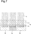
- Fig. 7 is a sectional view along line VII-VII of Fig. 6 .
- an input device 100 includes a housing 110 provided with a first opening 110a and a second opening 110b. Inside the housing 110, there are provided a touch sensor 120 disposed to block the first opening 110a of the housing 110, one photoelectric conversion cell 130 disposed in a position facing the touch sensor 120, a liquid crystal display unit 140 disposed to block the second opening 110b of the housing 110, a storage cell 150 connected to the photoelectric conversion cell 130, and a control unit 160 which is electrically connected to the touch sensor 120, the photoelectric conversion cell 130, and the liquid crystal display unit 140, and allows the liquid crystal display unit 140 to display the corresponding numeric characters on the basis of the manipulation of the touch sensor 120.
- the photoelectric conversion cell 130 includes a transparent electrode substrate 20, a counter substrate 30 facing the transparent electrode substrate 20, a ring-shaped sealing portion 40 joining the transparent electrode substrate 20 and the counter substrate 30 together, a power generation portion 50 which is provided on the transparent electrode substrate 20, and contains a dye, a non-power generation portion 70 provided on the transparent electrode substrate 20 to be adjacent to the power generation portion 50, and an electrolyte 60 provided between the transparent electrode substrate 20 and the counter substrate 30.
- the transparent electrode substrate 20 is provided on the touch sensor 120 side
- the counter substrate 30 is provided on a side facing away from the touch sensor 120, with respect to the transparent electrode substrate 20.
- the non-power generation portion 70 also functions as the display unit in this embodiment, and is provided to overlap with the display unit in the case of viewing the display unit and the non-power generation portion 70 in a thickness direction A of a substrate 121 of the touch sensor 120.
- the touch sensor 120 includes the substrate 121, an electrode 121a provided on the substrate 121, and a covering layer 122 provided on the substrate 121 to cover the electrode 121a.
- the non-power generation portion 70 which also functions as the display unit of the photoelectric conversion cell 130, is visible in the case of viewing the touch sensor 120 in the thickness direction A of the substrate 121 of the touch sensor 120 (a direction orthogonal to a surface of the substrate 121 of the touch sensor 120).
- ten non-power generation portions 70 are illustrated, and constitute numeric characters of "0" to "9", respectively.
- the non-power generation portion 70 and the electrode 121a as the display unit are arranged to overlap with each other in the case of being seen in the thickness direction A of the substrate 121 of the touch sensor 120.
- a wiring 125 is connected to the electrode 121a. At least a part of the wiring 125 extends from the electrode 121a and is disposed to overlap with the ring-shaped sealing portion 40 and to be along the ring-shaped sealing portion 40 in the case of viewing the wiring 125 and the ring-shaped sealing portion 40 in the thickness direction A of the substrate 121 of the touch sensor 120. Then, an end portion of the wiring 125 is connected to the control unit 160 (refer to Fig. 2 ).
- the non-power generation portion 70 which also functions as the display unit, is visible in the case of viewing the non-power generation portion 70 as the display unit in the thickness direction A of the substrate 121 of the touch sensor 120. That is, in the input device 100, the display unit is provided to be adjacent to the power generation portion 50 of the photoelectric conversion cell 130 and to overlap with the non-power generation portion 70. For this reason, as illustrated in Fig. 7 , when light L is incident on the photoelectric conversion cell 130 through the touch sensor 120, light is incident on the power generation portion 50 without forming a portion which becomes a shadow by the display unit. That is, in the power generation portion 50, a portion on which light is incident, and a portion on which light is not incident, are sufficiently prevented from being formed.
- the power generation portion 50 a bias in a generation amount of electrons is sufficiently prevented from being generated. As a result, deterioration of a dye is suppressed. Accordingly, in the input device 100, durability of the photoelectric conversion cell 130 is improved, and durability of the input device 100 is also improved.
- the touch sensor 120 includes the wiring 125 connected to the electrode 121a, and at least a part of the wiring 125 is disposed to overlap with the ring-shaped sealing portion 40 and to be along the ring-shaped sealing portion 40 in the case of viewing the wiring 125 and the ring-shaped sealing portion 40 in the thickness direction A of the substrate 121 of the touch sensor 120.
- the non-power generation portion 70 also functions as the display unit, and thus, it is not necessary to provide the display unit in the touch sensor 120. For this reason, it is possible to further reduce the thickness of the touch sensor 120, and to further reduce the size of the input device 100.
- the touch sensor 120 includes the substrate 121, the electrode 121a provided on the substrate 121, and the covering layer 122 provided on the substrate 121 to cover the electrode 121a.
- a resin film such as a PET film and a PEN film
- a substrate composed of an inorganic material such as glass, and the like can be used as the substrate 121.
- the electrode 121a is provided to overlap with the non-power generation portion 70 in the case of viewing the non-power generation portion 70 and the electrode 121a as the display unit in the thickness direction A of the substrate 121 of the touch sensor 120. It is preferable that the electrode 121a be composed of a mesh wiring. In this case, when the electrode 121a is provided to overlap with the power generation portion 50 in the case of viewing the power generation portion 50 and the electrode 121a in the thickness direction A of the substrate 121 of the touch sensor 120, it is possible to increase an incidence amount of light onto the power generation portion 50, and thus, it is possible to further improve photoelectric conversion characteristics of the photoelectric conversion cell 130.
- the electrode 121a is composed of the mesh wiring
- an opaque metal material such as silver or copper, or a carbon material
- a difference in transmittance of visible light between a portion passing through the mesh wiring and a portion passing through a portion other than the mesh wiring be less than or equal to 10%.
- it is possible to further decrease a variation in a power generation amount of the power generation portion 50 receiving light and thus, it is possible to increase service life of the photoelectric conversion cell 130. For this reason, it is possible to increase service life of the input device 100.
- the difference in the transmittance of the visible light be less than or equal to 5%.
- a line width of the mesh wiring is not particularly limited, and for example, may be less than or equal to 100 ⁇ m.
- the electrode 121a can be composed of a transparent metal material such as ITO or FTO.
- the covering layer 122 may be constituted by a transparent material.
- the transparent material include a transparent resin such as an epoxy resin, an acrylic resin, a polyester resin, a urethane resin, a vinyl resin, a silicone resin, a phenol resin or a polyimide resin.
- the covering layer 122 can be obtained by covering the substrate 121 with the transparent resin using a printing method or the like.
- the photoelectric conversion cell 130 has a transparent electrode substrate 20, the counter substrate 30, the sealing portion 40, the power generation portion 50, the non-power generation portion 70 and the electrolyte 60. Hereinafter, these will be described in detail.
- the transparent electrode substrate 20 comprises a transparent substrate 21, and a transparent conductive layer 22 which is provided on a side of the transparent substrate 21 facing the counter substrate 30 and serves as an electrode.
- the material constituting the transparent substrate 21 may be a transparent insulating material, for example, and examples of such a transparent material include glass such as borosilicate glass, soda lime glass, glass which is made of soda lime and whose iron component is less than that of ordinary soda lime glass, and quartz glass, polyethylene terephthalate (PET), polyethylene naphthalate (PEN), polycarbonate (PC), and polyethersulfone (PES).
- the thickness of the transparent substrate 21 is appropriately determined depending on the size of the photoelectric conversion cell 130 and is not particularly limited, but it may be set to the range of from 0.050 to 10 mm, for example.
- the material constituting the transparent conductive layer 22 examples include a conductive metal oxide such as indium-tin-oxide (ITO), tin oxide (SnO 2 ), and fluorine-doped-tin-oxide (FTO).
- the transparent conductive layer 22 may be constituted by a single layer or a laminate consisting of a plurality of layers containing different conductive metal oxides. It is preferable that the transparent conductive layer 22 contain FTO since the FTO exhibits high heat resistance and chemical resistance in a case in which the transparent conductive layer 22 is constituted by a single layer.
- the thickness of the transparent conductive layer 22 may be set to the range of from 0.01 to 2 ⁇ m, for example.
- the counter substrate 30, which is composed of a counter electrode in this embodiment, comprises the conductive substrate 31 and the catalyst layer 32 which is provided on a side of the conductive substrate 31 facing the transparent electrode substrate 20 and contributes to reduction of the electrolyte 60.
- the conductive substrate 31 may be constituted by a corrosion-resistant metal material such as titanium, nickel, molybdenum, tungsten, aluminum, or stainless steel. Moreover, the conductive substrate 31 may be a laminate in which a conductive layer composed of a conductive oxide such as ITO or FTO is formed as an electrode on the transparent substrate 21 described above.
- the thickness of the conductive substrate 31 is appropriately determined depending on the size of the photoelectric conversion cell 130, and is not particularly limited, but may be set to 0.005 mm to 0.1 mm, for example.
- the catalyst layer 32 is constituted by a conductive material.
- the conductive material include a metal material such as platinum, a carbon-based material and a conductive polymer.
- a carbon nanotube is preferably used as the carbon-based material.
- sealing portion 40 examples include a resin such as a thermoplastic resin including a modified polyolefin resin or a vinyl alcohol polymer, or an ultraviolet curable resin.
- modified polyolefin resin include an ionomer, an ethylene-vinyl acetic anhydride copolymer, an ethylene-methacrylic acid copolymer and an ethylene-vinyl alcohol copolymer. These can be used singly or in a combination of two or more types of such resins.
- the power generation portion 50 includes an oxide semiconductor layer and a dye supported on the oxide semiconductor layer.
- the oxide semiconductor layer is composed of oxide semiconductor particles.
- the oxide semiconductor particles are composed of, for example, titanium oxide (TiO 2 ) , zinc oxide (ZnO), tungsten oxide (WO 3 ), niobium oxide (Nb 2 O 5 ), strontium titanate (SrTiO 3 ), tin oxide (SnO 2 ), indium oxide (In 3 O 3 ), zirconium oxide (ZrO 2 ), tallium oxide (Ta 2 O 5 ), lanthanum oxide (La 2 O 3 ), yttrium oxide (Y 2 O 3 ), holmium oxide (Ho 2 O 3 ), bismuth oxide (Bi 2 O 3 ), cerium oxide (CeO 2 ), aluminum oxide (Al 2 O 3 ) or two or more kinds of these.
- the thickness of the oxide semiconductor layer 50 may be set to 0.1 ⁇ m to 100 ⁇ m, for example.
- a photosensitizing dye such as a ruthenium complex having a ligand including a bipyridine structure or a terpyridine structure, an organic dye including porphyrin, eosin, rhodamine or merocyanine; or an organic-inorganic composite dye including a halogenated lead-based perovskite crystal are exemplified.
- a ruthenium complex having a ligand including a bipyridine structure or a terpyridine structure is preferable. In this case, it is possible to further improve the photoelectric conversion characteristics of the photoelectric conversion cell 130. Furthermore, in a case using a photosensitizing dye as the dye, the photoelectric conversion cell 130 becomes a dye-sensitized photoelectric conversion cell.
- the non-power generation portion 70 may not have a photoelectric conversion function. However, in this embodiment, the non-power generation portion 70 also functions as the display unit, and thus, it is necessary that the non-power generation portion 70 can be viewed by being distinguished from the power generation portion 50 in the case of viewing the non-power generation portion 70 and the power generation portion 50 in the thickness direction A of the substrate 121 of the touch sensor 120.
- the non-power generation portion 70 is composed including an insulating portion 71 containing a coloring material.
- the coloring material indicates a substance having an absorption peak in a wavelength range of visible light.
- the insulating portion 71 contains an insulating material.
- an inorganic insulating material such as glass frit
- an organic insulating material such as a thermosetting resin (a polyimide resin or the like) and a thermoplastic resin are exemplified as the insulating material.
- the inorganic insulating material such as glass frit is preferable as the insulating material.
- a dimensional change of the insulating portion 71 further decreases, compared to a case where the insulating material is not the inorganic insulating material.
- the coloring material contained in the insulating portion 71 may be any coloring material as long as the coloring material colors the insulating portion 71, and examples of such the coloring material include, for example, an oxide of a transition metal, a carbon-based material, an organic dye, and the like. These can be used singly or in a combination of two or more types of such coloring materials. Among them, the oxide of the transition metal is preferable as the coloring material. In this case, it is possible to more sufficiently prevent the coloring material from being dissolved in the electrolyte 60.
- copper oxide, iron oxide, cobalt oxide, manganese oxide, and the like are exemplified as the oxide of the transition metal. These can be used singly or in a combination of two or more types of such oxides.
- a content ratio of the coloring material in the insulating portion 71 is not particularly limited, but is preferably greater than or equal to 5 mass%. In this case, it is possible to further decrease light transmittivity, compared to a case where the content ratio of the coloring material in the insulating portion 71 is less than 5 mass%.
- the content ratio of the coloring material in the insulating portion 71 is more preferably greater than or equal to 7 mass%, and is particularly preferably greater than or equal to 9 mass%. However, it is preferable that the content ratio of the coloring material in the insulating portion 71 is less than or equal to 30 mass%.
- the coloring material can be more sufficiently prevented from being dissolved in the electrolyte 60, compared to a case where the content ratio of the coloring material in the insulating portion 71 is greater than 30 mass%.
- the content ratio of the coloring material in the insulating portion 71 is more preferably less than or equal to 27 mass%, and is particularly preferably less than or equal to 25 mass%.
- the non-power generation portion 70 further includes a covering portion 72 covering the insulating portion 71, in addition to the insulating portion 71 containing the coloring material.
- the insulating portion 71 is covered with the covering portion 72, and thus, it is possible to sufficiently prevent the insulating portion 71 containing the coloring material from being in contact with the electrolyte 60 and being dissolved in the electrolyte 60. Accordingly, in the photoelectric conversion cell 130, it is possible to reduce the amount of coloring material entering the electrolyte 60.
- the covering portion 72 is effective in a case where the total area of the non-power generation portion 70 within a region surrounded by the sealing portion 40 (within a region surrounded by a broken line of Fig. 3 ) is greater than or equal to 10%.
- the covering portion 72 is composed of an insulating material.
- the same insulating material as that constituting the insulating portion 71 can be used as the insulating material.
- the insulating material constituting the covering portion 72 may be identical to or different from the insulating material constituting the insulating portion 71.
- a content ratio of the coloring material in the covering portion 72 may be less than the content ratio of the coloring material in the insulating portion 71, or may be greater than or equal to the content ratio of the coloring material in the insulating portion 71, but it is preferable that the content ratio of the coloring material in the covering portion 72 be less than the content ratio of the coloring material in the insulating portion 71. In this case, the coloring material in the non-power generation portion 70 is more sufficiently prevented from being mixed into the electrolyte 60, compared to a case where the content ratio of the coloring material in the covering portion 72 is greater than or equal to the content ratio of the coloring material in the insulating portion 71.
- the content ratio of the coloring material in the covering portion 72 may be 0 mass%. That is, the covering portion 72 may not contain the coloring material.
- the content ratio of the coloring material in the covering portion 72 may be greater than 0 mass% as long as the content ratio is less than the content ratio in the insulating portion 71. That is, in a case where the content ratio of the coloring material in the covering portion 72 is the content ratio less than the content ratio in the insulating portion 71, the covering portion 72 may contain the coloring material.
- the coloring material in the covering portion 72 typically means the same coloring material as the coloring material contained in the insulating portion 71.
- the coloring material in the covering portion 72 is also the oxide of the transition metal, if the coloring material contained in the insulating portion 71 is the oxide of the transition metal.
- the thickness of the covering portion 72 from a surface of the insulating portion 71 is typically 3 ⁇ m to 20 ⁇ m, and is preferably 5 ⁇ m to 10 ⁇ m.
- an area of a region in which the covering portion 72 is not provided be less than or equal to 10%.
- an area of the region described above is more preferably less than or equal to 8%, and is particularly preferably less than or equal to 6%.
- the electrolyte 60 contains a redox couple and an organic solvent. It is possible to use acetonitrile, methoxy acetonitrile, methoxy propionitrile, propionitrile, ethylene carbonate, propylene carbonate, diethyl carbonate, ⁇ -butyrolactone, valeronitrile, or pivalonitrile as the organic solvent.
- redox couple examples include a redox couple such as a zinc complex, an iron complex, and a cobalt complex in addition to a redox couple containing a halogen atom such as iodide ion/polyiodide ion (for example, I - /I 3 - ) or bromide ion/polybromide ion.
- iodide ion/polyiodide ion can be formed by iodine (I 2 ) and a salt (ionic liquid or a solid salt) containing an iodide (I - ) as an anion.
- ionic liquid having an iodide as an anion only iodine may be added.
- a salt containing iodide (I - ) as an anion such as LiI or tetrabutylammonium iodide may be added.
- the electrolyte 60 may use ionic liquid instead of the organic solvent.
- a known iodine salt such as a pyridinium salt, an imidazolium salt, or a triazolium salt is used.
- an iodine salt for example, 1-hexyl-3-methylimidazolium iodide, 1-ethyl-3-propylimidazolium iodide, 1-ethyl-3-methylimidazolium iodide, 1,2-dimethyl-3-propylimidazolium iodide, 1-butyl-3-methylimidazolium iodide, or 1-methyl-3-propylimidazolium iodide is preferably used.
- the electrolyte 60 may use a mixture of the above-mentioned ionic liquid and the above-mentioned organic solvent instead of the above-mentioned organic solvent.
- an additive to the electrolyte 60.
- the additive include benzimidazole such as 1-methylbenzimidazole (NMB) or 1-butylbenzimidazole (NBB), LiI, tetrabutylammonium iodide, 4-t-butylpyridine and guanidium thiocyanate.
- benzimidazole is preferable as the additive.
- a nanocomposite gel electrolyte which is a quasi-solid electrolyte obtained by kneading nanoparticles such as SiO 2 , TiO 2 and carbon nanotubes with the above-mentioned electrolyte to form a gel-like form may be used, or an electrolyte gelled using an organic gelling agent such as polyvinylidene fluoride, a polyethylene oxide derivative and an amino acid derivative may also be used.
- the non-power generation portion 70 is composed by including the insulating portion 71 containing the coloring material, but the non-power generation portion 70 is not necessarily limited to a non-power generation portion which is composed including the insulating portion 71 containing the coloring material.
- the non-power generation portion 70 may be composed of a mere space as long as the non-power generation portion 70 can be viewed by being distinguished from the power generation portion 50 in the case of viewing the non-power generation portion 70 and the power generation portion 50 in the thickness direction A of the substrate 121 of the touch sensor 120.
- a light reflection layer is provided on the counter substrate 30 side, with respect to the power generation portion 50, and the light reflection layer can be viewed by being distinguished from the power generation layer 50, a portion of the light reflection layer, which can be viewed through the space in the case of viewing the non-power generation portion 70 in the thickness direction A of the substrate 121 of the touch sensor 120, is the non-power generation portion 70.
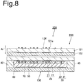
- the non-power generation portion 70 of the photoelectric conversion cell 130 also functions as the display unit, and the touch sensor 120 does not include the display unit, but like an input device 200 illustrated in Fig. 8 , a touch sensor 220 may include a display unit 124.
- a touch sensor 220 may include a display unit 124.
- the power generation portion 50 a bias in the generation amount of the electrons is sufficiently prevented from being generated. As a result, the deterioration of the dye is suppressed. Accordingly, even in the input device 200 illustrated in Fig. 8 , the durability of the photoelectric conversion cell 130 is improved, and the durability of the input device 200 is also improved. In addition, in the input device 200 illustrated in Fig. 8 , the non-power generation portion 70 is not visible in the case of viewing the non-power generation portion 70 and the display unit 124 in the thickness direction A of the substrate 121 of the touch sensor 220, and thus, it is not necessary that the non-power generation portion 70 contain the coloring material.
- the coloring material in the non-power generation portion 70 is sufficiently prevented from being mixed into the electrolyte 60.
- the photoelectric conversion cell 130 it is possible to suppress deterioration in the photoelectric conversion characteristics due to the mixing of the coloring material, and to more sufficiently improve the durability.
- the display unit 124 be disposed on the inside of an outline forming the non-power generation portion 70 in the case of viewing the display unit 124 and the non-power generation portion 70 in the thickness direction A of the substrate 121 of the touch sensor 220.
- the wiring 125 is disposed to overlap with the ring-shaped sealing portion 40 and to be along the ring-shaped sealing portion 40 in the case of viewing the wiring 125 and the ring-shaped sealing portion 40 in the thickness direction A of the substrate 121 of the touch sensor 120, but the wiring 125 may not be necessarily disposed to overlap with the ring-shaped sealing portion 40 and to be along the ring-shaped sealing portion 40.
- the non-power generation portion 70 also functions as the display unit, and the display units constitute the numeric characters of "0" to "9", respectively, but the display unit is not limited to the numeric character, and may be information such as characters, diagrams, symbols, or a combination thereof.
- the oxide semiconductor layer 50 is provided on the transparent electrode substrate 20 in the photoelectric conversion cell 130, but the oxide semiconductor layer 50 may be provided on the counter substrate 30. In this case, a catalytic layer 32 is provided on the transparent electrode substrate 20.
- the counter substrate 30 is composed of a counter electrode, and the transparent electrode substrate 20 and the counter substrate 30 are linked by the sealing portion 40, but in a case where a porous insulating layer impregnated with the electrolyte 60 and an electrode layer are sequentially laminated on the oxide semiconductor layer 50 between the transparent electrode substrate 20 and the counter substrate 30, the counter substrate 30 may be composed of an insulating base material instead of the counter electrode.
- the input device 100 includes the housing 110, the liquid crystal display unit 140, the storage battery 150, and the control unit 160, but these are not necessarily required, and can be omitted.
- the input device 100 includes one photoelectric conversion cell 130, but the input device 100 may include a plurality of photoelectric conversion cells 130.
- the plurality of photoelectric conversion cells 130 may be connected in series, or may be connected in parallel.
- a laminated body was prepared in which a transparent conductive layer formed of FTO and having a thickness of 1 ⁇ m was formed on a transparent substrate formed of glass and having a thickness of 1 mm.
- a paste for forming an insulating portion containing glass frit and a coloring material was applied onto the transparent conductive layer by screen printing to form a character of "2", and was dried, and thus, a precursor of an insulating portion was formed.
- the coloring material was contained such that a content ratio of the coloring material in the glass frit was 15 mass%.
- a coloring material formed of iron oxide, copper oxide, and manganese oxide was used as the coloring material.
- a precursor of a covering portion was formed to cover the entire precursor of the insulating portion.
- the precursor of the covering portion was formed by applying and drying a paste for forming a covering portion formed of glass frit. At this time, a content ratio of a coloring material in the paste for forming a covering portion was 0 mass%.
- a precursor of an oxide semiconductor layer constituting a power generation portion was formed on the transparent conductive layer. However, at this time, the precursor of the covering portion was not covered.
- the precursor of the oxide semiconductor layer was formed by applying a paste for forming an oxide semiconductor layer containing titania particles by screen printing and drying the paste.
- the precursor of the insulating portion, the precursor of the covering portion, and the precursor of the oxide semiconductor layer were fired at 500°C for 1 hour.
- an electrode structure including a non-power generation portion formed of the insulating portion and the covering portion, and the oxide semiconductor layer constituting the power generation portion was obtained.
- the electrode structure described above was dipped in a dye solution, in which 0.2 mM of a photosensitized dye formed of N719 was contained, and a solvent was a mixed solvent obtained by mixing acetonitrile and tertbutanol at a volume ratio of 1 : 1, for a full day and night, and then, was taken out and dried, and thus, the photosensitized dye was supported on the oxide semiconductor layer.
- a dye solution in which 0.2 mM of a photosensitized dye formed of N719 was contained
- a solvent was a mixed solvent obtained by mixing acetonitrile and tertbutanol at a volume ratio of 1 : 1, for a full day and night, and then, was taken out and dried, and thus, the photosensitized dye was supported on the oxide semiconductor layer.
- an electrolyte formed of 2 M of 1-hexyl-3-methyl imidazolium iodide, 0.002 M of I 2 , 0.3 M of n-methyl benzimidazole, and 0.1 M of guanidium thiocyanate in a solvent formed of 3-methoxy propionitrile was dropped on the oxide semiconductor layer, and then dried, and thus, the electrolyte was disposed.
- the sealing portion forming body was obtained by preparing one resin film for sealing formed of maleic anhydride-modified polyethylene (Product Name: Bynel, manufactured by DuPont), and by forming one quadrangular opening on the resin film for sealing. At this time, the sealing portion forming body was produced such that the opening had a dimension of 4.2 cm ⁇ 9.7 cm ⁇ 60 ⁇ m and the width of the sealing portion forming body was 1.8 mm.
- the sealing portion forming body was overlapped with the electrode structure described above, and then, the sealing portion forming body was heated and melted, and thus, was adhered onto the electrode structure described above.
- One counter substrate was prepared.
- One counter substrate was prepared by forming a catalytic layer formed of platinum, on a titanium foil of 4.6 cm ⁇ 10.0 cm ⁇ 40 ⁇ m, by a sputtering method.
- the sealing portion forming body adhered onto the electrode structure described above and the counter substrate were overlapped to face each other. Then, in such a state, the sealing portion forming body was heated and melted while being pressurized. Thus, the sealing portion was formed between the electrode structure and the counter substrate.
- a touch sensor was prepared as described below. That is, first, a substrate formed of a PET film was prepared, and an electrode was formed in a region of 42 mm ⁇ 97 mm on a surface of the substrate by screen printing. At this time, the electrode was formed such that a mesh wiring has a line width of 4 ⁇ m and a difference in transmittance of visible light between a portion passing through the mesh wiring and a portion passing through a portion other than the mesh wiring was 10%. In addition, from the electrode, a wiring was formed such that a line width was 10 ⁇ m. At this time, the wiring extended to a region of 0.3 mm from an edge portion of the substrate, and was formed to be disposed along the region from there.
- the substrate described above was covered with the covering layer formed of a PET film to cover the electrode.
- the touch sensor was obtained.
- the photoelectric conversion cell and the touch sensor obtained as described above were laminated on each other.
- the photoelectric conversion cell and the touch sensor were fixed to each other by allowing the circumferences to adhere to each other with an adhesive agent.
- the non-power generation portion was overlapped with the electrode of the touch sensor in the case of viewing the non-power generation portion in the thickness direction of the substrate of the touch sensor. Thus, an input device was produced.
- An input device was produced by the same method as that of Example 1, except that a precursor of an insulating portion containing glass frit and a coloring material was not formed on a transparent conductive layer, and a precursor of a covering portion was not formed to cover the entire precursor of the insulating portion, and thus, a non-power generation portion was not formed.
Landscapes
- Engineering & Computer Science (AREA)
- General Engineering & Computer Science (AREA)
- Theoretical Computer Science (AREA)
- Human Computer Interaction (AREA)
- Physics & Mathematics (AREA)
- General Physics & Mathematics (AREA)
- Power Engineering (AREA)
- Microelectronics & Electronic Packaging (AREA)
- Photovoltaic Devices (AREA)
- Hybrid Cells (AREA)
- Input From Keyboards Or The Like (AREA)
Abstract
Description
- The present invention relates to an input device including a touch sensor.
- A photoelectric conversion element such as a dye-sensitized solar cell or an organic thin film solar cell is expected as a power source of various devices. In many cases, the photoelectric conversion element is typically used only as a cell, but recently, a case has also increased in which the photoelectric conversion element is included in an input device including a touch sensor, as a power source of the input device.
- For example, in
Patent Document 1 described below, an input device including a dye-sensitized solar cell, and a touch sensor facing the dye-sensitized solar cell, is disclosed. In this publication, it is also disclosed that the dye-sensitized solar cell includes a transparent electrode substrate provided on a side facing the touch sensor, a counter substrate which is provided on a side facing away from the touch sensor, with respect to the transparent electrode substrate, and faces the transparent electrode substrate, and a porous semiconductor layer provided between the transparent electrode substrate and the counter substrate. - Patent Document 1:
JP 2013-89527 A - However, the input device described in
Patent Document 1 described above, has had the following problems. - That is, the input device described in
Patent Document 1, has room for improvement in durability. - The invention has been made in consideration of the circumstances described above, and an object thereof is to provide an input device capable of improving durability.
- As a result of studying the reason of the problems described above, the present inventors have considered as follows. That is, first, the touch sensor, for example, typically includes a display unit such as "1" and "2", and the display unit overlaps with a porous semiconductor layer of a dye-sensitized solar cell in the case of viewing the display unit in a thickness direction of a substrate constituting the touch sensor. Here, when light incident from the touch sensor is incident on the dye-sensitized solar cell, the porous semiconductor layer is divided into a portion which becomes a shadow of the display unit, and a portion on which light is incident without being a shadow. The present inventors have considered that a bias is generated at this time in a generation amount of electrons between the portion which becomes the shadow and the portion which does not become the shadow, and as a result, a dye deteriorates, and thus, power generation performance is degraded. Therefore, as a result of conducting intensive studies, the present inventors have completed the invention.
- That is, the invention is an input device including: at least one photoelectric conversion cell; and a touch sensor which faces the at least one photoelectric conversion cell, and includes a substrate, a display unit being visible in the case of viewing the touch sensor and the photoelectric conversion cell in a thickness direction of the substrate of the touch sensor, in which the photoelectric conversion cell includes, a transparent electrode substrate provided on the touch sensor side, a counter substrate which is provided on a side facing away from the touch sensor, with respect to the transparent electrode substrate, and faces the transparent electrode substrate, a power generation portion which is provided between the transparent electrode substrate and the counter substrate, and contains a dye, and a non-power generation portion provided to be adjacent to the power generation portion and to overlap with the display unit in the case of viewing the power generation portion and the display unit in the thickness direction of the substrate of the touch sensor.
- According to the input device, in the case of viewing the power generation portion and the display unit in the thickness direction of the substrate of the touch sensor, the display unit is provided to be adjacent to the power generation portion of the photoelectric conversion cell and to overlap with the non-power generation portion. For this reason, when light is incident on the photoelectric conversion cell through the touch sensor, light is incident on the power generation portion other than the display unit without forming a portion which becomes a shadow by the display unit. That is, a portion on which light is incident, and a portion on which light is not incident are sufficiently prevented from being formed in the power generation portion. As a result, in the power generation portion, a bias in a generation amount of electrons is sufficiently prevented from being generated. As a result, deterioration of the dye is suppressed. Therefore, according to the invention, it is possible to improve durability of the photoelectric conversion cell, and also to improve durability of the input device.
- In the input device described above, it is preferable that the display unit be included in a photoelectric conversion cell or a touch panel.
- In the input device described above, it is preferable that the photoelectric conversion cell further include a ring-shaped sealing portion joining the transparent electrode substrate and the counter substrate together, the touch sensor include an electrode which is provided on the substrate, and is provided to overlap with the display unit in the case of viewing the touch sensor and the photoelectric conversion cell in the thickness direction of the substrate of the touch sensor, and a wiring connected to the electrode, and at least a part of the wiring be disposed to overlap with the ring-shaped sealing portion and to be along the ring-shaped sealing portion in the case of viewing the wiring and the ring-shaped sealing portion in the thickness direction of the substrate of the touch sensor.
- In this case, since at least a part of the wiring is disposed to overlap with the ring-shaped sealing portion and to be along the ring-shaped sealing portion in the case of viewing the wiring and the ring-shaped sealing portion in the thickness direction of the substrate of the touch sensor, it is possible to decrease an area of the wiring blocking the incidence of light onto the power generation portion, and to increase an aperture ratio.
- In the input device described above, it is preferable that in the touch sensor, the electrode be composed of a mesh wiring.
- In this case, in a case where the electrode is provided to overlap with the power generation portion in the case of viewing the power generation portion and the electrode in the thickness direction of the substrate of the touch sensor, it is possible to increase an incidence amount of light onto the power generation portion, and to further improve photoelectric conversion characteristics of the photoelectric conversion cell.
- In the input device described above, it is preferable that a difference in transmittance of visible light between a portion passing through the mesh wiring and a portion passing through a portion other than the mesh wiring is less than or equal to 10%.
- In this case, since it is possible to further decrease a variation in a power generation amount of the power generation portion receiving light, compared to a case where a difference in transmittance of visible light between the portion passing through the mesh wiring and the portion passing through the portion other than the mesh wiring is greater than 10%, it is possible to further increase service life of the photoelectric conversion cell. For this reason, it is possible to further increase service life of the input device.
- In the input device described above, it is preferable that the photoelectric conversion cell include an electrolyte between the transparent electrode substrate and the counter substrate, and the non-power generation portion include an insulating portion containing a coloring material, and a covering portion covering the insulating portion.
- In this case, since in the non-power generation portion, the insulating portion is covered with the covering portion, it is more sufficiently prevented that the insulating portion containing the coloring material is in contact with the electrolyte and then the coloring material is dissolved in the electrolyte. Accordingly, it is possible to reduce the amount of coloring material entering the electrolyte. For this reason, according to the input device of the invention, it is possible to suppress deterioration in photoelectric conversion characteristics due to the mixing of the coloring material, and to more sufficiently improve the durability.
- In the input device described above, it is preferable that the insulating portion contain an insulating material, and the insulating material contain an inorganic insulating material.
- In this case, a dimensional change of the insulating portion further decreases, compared to a case where the insulating material does not contain the inorganic insulating material.
- In the input device described above, it is preferable that the coloring material be composed of an oxide of a transition metal.
- In this case, it is possible to more sufficiently prevent the coloring material from being dissolved in the electrolyte.
- In the input device described above, it is preferable that a content ratio of the coloring material in the covering portion is less than a content ratio of the coloring material in the insulating portion.
- In this case, the coloring material in the non-power generation portion is sufficiently prevented from being mixed into the electrolyte, compared to a case where the content ratio of the coloring material in the covering portion is greater than or equal to the content ratio of the coloring material in the insulating portion. For this reason, in the photoelectric conversion cell, it is possible to suppress deterioration in the photoelectric conversion characteristics due to the mixing of the coloring material, and to more sufficiently improve the durability.
- In the input device described above, it is preferable that in a surface of the insulating portion excluding an interface between the insulating portion and the transparent electrode substrate from the surface, an area of a region in which the covering portion is not provided, be less than or equal to 10%.
- In this case, even in a case where the coloring material in the insulating portion is dissolved into the electrolyte, it is possible to more sufficiently reduce an influence on the durability of the photoelectric conversion cell, compared to a case where the area of the region described above is greater than 10%.
- In the input device described above, it is preferable that the non-power generation portion also functions as the display unit.
- In this case, since it is not necessary to provide the display unit in the touch sensor by the non-power generation portion also functioning as the display unit, it is possible to further reduce the thickness of the touch sensor, and to further reduce the size of the input device.
- In the input device described above, it is preferable that the photoelectric conversion cell include an electrolyte between the transparent electrode substrate and the counter substrate, and the touch sensor include the display unit.
- In this case, in the input device, the non-power generation portion is not visible in the case of viewing the non-power generation portion and the display unit in the thickness direction of the substrate of the touch sensor, and thus, it is not necessary for the non-power generation portion to contain the coloring material. For this reason, the coloring material in the non-power generation portion is sufficiently prevented from being mixed into the electrolyte. For this reason, in the photoelectric conversion cell, it is possible to suppress deterioration in the photoelectric conversion characteristics due to the mixing of the coloring material, and to more sufficiently improve the durability.
- In the input device described above, for example, the at least one photoelectric conversion cell is composed of a plurality of photoelectric conversion cells, and the plurality of photoelectric conversion cells are connected in series.
- According to the invention, an input device capable of improving durability is provided.
-
-
Fig. 1 is a plan view illustrating one embodiment of an input device of the invention; -
Fig. 2 is a sectional view schematically illustrating the input device ofFig. 1 ; -
Fig. 3 is a plan view illustrating a part of the input device ofFig. 1 ; -
Fig. 4 is a sectional view along line IV-IV ofFig. 3 ; -
Fig. 5 is a sectional view illustrating a non-power generation portion ofFig. 4 ; -
Fig. 6 is a plan view in the case of viewing a power generation portion and a non-power generation portion of a photoelectric conversion element ofFig. 2 from a touch sensor side; -
Fig. 7 is a sectional view along line VII-VII ofFig. 6 ; and -
Fig. 8 is a sectional end view illustrating main parts of another embodiment of an input device of the invention. - Hereinafter, an embodiment of an input device according to the invention will be described in detail, with reference to
Fig. 1 to Fig. 7 . Furthermore,Fig. 1 is a plan view illustrating a preferred embodiment of the input device of the invention,Fig. 2 is a sectional view schematically illustrating the input device ofFig. 1 ,Fig. 3 is a plan view illustrating a part of the input device ofFig. 1 ,Fig. 4 is a sectional view along line IV-IV ofFig. 3 ,Fig. 5 is a sectional view illustrating a non-power generation portion ofFig. 4 ,Fig. 6 is a plan view in the case of viewing a power generation portion and a non-power generation portion of a photoelectric conversion element ofFig. 2 from a touch sensor side, andFig. 7 is a sectional view along line VII-VII ofFig. 6 . - As illustrated in
Fig. 1 andFig. 2 , aninput device 100 includes ahousing 110 provided with afirst opening 110a and asecond opening 110b. Inside thehousing 110, there are provided atouch sensor 120 disposed to block thefirst opening 110a of thehousing 110, onephotoelectric conversion cell 130 disposed in a position facing thetouch sensor 120, a liquidcrystal display unit 140 disposed to block thesecond opening 110b of thehousing 110, astorage cell 150 connected to thephotoelectric conversion cell 130, and acontrol unit 160 which is electrically connected to thetouch sensor 120, thephotoelectric conversion cell 130, and the liquidcrystal display unit 140, and allows the liquidcrystal display unit 140 to display the corresponding numeric characters on the basis of the manipulation of thetouch sensor 120. - As illustrated in
Fig. 4 andFig. 6 , thephotoelectric conversion cell 130 includes atransparent electrode substrate 20, acounter substrate 30 facing thetransparent electrode substrate 20, a ring-shapedsealing portion 40 joining thetransparent electrode substrate 20 and thecounter substrate 30 together, apower generation portion 50 which is provided on thetransparent electrode substrate 20, and contains a dye, anon-power generation portion 70 provided on thetransparent electrode substrate 20 to be adjacent to thepower generation portion 50, and anelectrolyte 60 provided between thetransparent electrode substrate 20 and thecounter substrate 30. Here, thetransparent electrode substrate 20 is provided on thetouch sensor 120 side, and thecounter substrate 30 is provided on a side facing away from thetouch sensor 120, with respect to thetransparent electrode substrate 20. In addition, thenon-power generation portion 70 also functions as the display unit in this embodiment, and is provided to overlap with the display unit in the case of viewing the display unit and thenon-power generation portion 70 in a thickness direction A of asubstrate 121 of thetouch sensor 120. - On the other hand, as illustrated in
Fig. 3 andFig. 4 , thetouch sensor 120 includes thesubstrate 121, anelectrode 121a provided on thesubstrate 121, and acovering layer 122 provided on thesubstrate 121 to cover theelectrode 121a. Here, in thetouch sensor 120, thenon-power generation portion 70 which also functions as the display unit of thephotoelectric conversion cell 130, is visible in the case of viewing thetouch sensor 120 in the thickness direction A of thesubstrate 121 of the touch sensor 120 (a direction orthogonal to a surface of thesubstrate 121 of the touch sensor 120). InFig. 1 andFig. 3 , tennon-power generation portions 70 are illustrated, and constitute numeric characters of "0" to "9", respectively. Furthermore, thenon-power generation portion 70 and theelectrode 121a as the display unit are arranged to overlap with each other in the case of being seen in the thickness direction A of thesubstrate 121 of thetouch sensor 120. - In addition, as illustrated in
Fig. 1 andFig. 3 , in thetouch sensor 120, awiring 125 is connected to theelectrode 121a. At least a part of thewiring 125 extends from theelectrode 121a and is disposed to overlap with the ring-shapedsealing portion 40 and to be along the ring-shapedsealing portion 40 in the case of viewing thewiring 125 and the ring-shapedsealing portion 40 in the thickness direction A of thesubstrate 121 of thetouch sensor 120. Then, an end portion of thewiring 125 is connected to the control unit 160 (refer toFig. 2 ). - According to the
input device 100, thenon-power generation portion 70 which also functions as the display unit, is visible in the case of viewing thenon-power generation portion 70 as the display unit in the thickness direction A of thesubstrate 121 of thetouch sensor 120. That is, in theinput device 100, the display unit is provided to be adjacent to thepower generation portion 50 of thephotoelectric conversion cell 130 and to overlap with thenon-power generation portion 70. For this reason, as illustrated inFig. 7 , when light L is incident on thephotoelectric conversion cell 130 through thetouch sensor 120, light is incident on thepower generation portion 50 without forming a portion which becomes a shadow by the display unit. That is, in thepower generation portion 50, a portion on which light is incident, and a portion on which light is not incident, are sufficiently prevented from being formed. For this reason, in thepower generation portion 50, a bias in a generation amount of electrons is sufficiently prevented from being generated. As a result, deterioration of a dye is suppressed. Accordingly, in theinput device 100, durability of thephotoelectric conversion cell 130 is improved, and durability of theinput device 100 is also improved. - In addition, in the
input device 100, thetouch sensor 120 includes thewiring 125 connected to theelectrode 121a, and at least a part of thewiring 125 is disposed to overlap with the ring-shapedsealing portion 40 and to be along the ring-shapedsealing portion 40 in the case of viewing thewiring 125 and the ring-shapedsealing portion 40 in the thickness direction A of thesubstrate 121 of thetouch sensor 120. - For this reason, it is possible to decrease an area of the
wiring 125 blocking the incidence of light onto thepower generation portion 50, and to increase an aperture ratio. - Further, in the
input device 100, thenon-power generation portion 70 also functions as the display unit, and thus, it is not necessary to provide the display unit in thetouch sensor 120. For this reason, it is possible to further reduce the thickness of thetouch sensor 120, and to further reduce the size of theinput device 100. - Next, the
touch sensor 120 and thephotoelectric conversion cell 130 will be described in detail. - As described above, the
touch sensor 120 includes thesubstrate 121, theelectrode 121a provided on thesubstrate 121, and thecovering layer 122 provided on thesubstrate 121 to cover theelectrode 121a. - For example, a resin film such as a PET film and a PEN film, a substrate composed of an inorganic material such as glass, and the like can be used as the
substrate 121. - The
electrode 121a is provided to overlap with thenon-power generation portion 70 in the case of viewing thenon-power generation portion 70 and theelectrode 121a as the display unit in the thickness direction A of thesubstrate 121 of thetouch sensor 120. It is preferable that theelectrode 121a be composed of a mesh wiring. In this case, when theelectrode 121a is provided to overlap with thepower generation portion 50 in the case of viewing thepower generation portion 50 and theelectrode 121a in the thickness direction A of thesubstrate 121 of thetouch sensor 120, it is possible to increase an incidence amount of light onto thepower generation portion 50, and thus, it is possible to further improve photoelectric conversion characteristics of thephotoelectric conversion cell 130. In a case where theelectrode 121a is composed of the mesh wiring, an opaque metal material such as silver or copper, or a carbon material can be used as theelectrode 121a. Here, in a case where light is incident in the thickness direction A of thesubstrate 121 of thetouch sensor 120, it is preferable that a difference in transmittance of visible light between a portion passing through the mesh wiring and a portion passing through a portion other than the mesh wiring be less than or equal to 10%. In this case, it is possible to further decrease a variation in a power generation amount of thepower generation portion 50 receiving light, and thus, it is possible to increase service life of thephotoelectric conversion cell 130. For this reason, it is possible to increase service life of theinput device 100. It is more preferable that the difference in the transmittance of the visible light be less than or equal to 5%. In a case where theelectrode 121a is composed of the mesh wiring, a line width of the mesh wiring is not particularly limited, and for example, may be less than or equal to 100 µm. However, it is not necessary that theelectrode 121a be composed of the mesh wiring. For example, theelectrode 121a can be composed of a transparent metal material such as ITO or FTO. - The
covering layer 122 may be constituted by a transparent material. Examples of such the transparent material include a transparent resin such as an epoxy resin, an acrylic resin, a polyester resin, a urethane resin, a vinyl resin, a silicone resin, a phenol resin or a polyimide resin. - The
covering layer 122 can be obtained by covering thesubstrate 121 with the transparent resin using a printing method or the like. - Next, the
photoelectric conversion cell 130 will be described in detail. - The
photoelectric conversion cell 130 has atransparent electrode substrate 20, thecounter substrate 30, the sealingportion 40, thepower generation portion 50, thenon-power generation portion 70 and theelectrolyte 60. Hereinafter, these will be described in detail. - The
transparent electrode substrate 20 comprises atransparent substrate 21, and a transparentconductive layer 22 which is provided on a side of thetransparent substrate 21 facing thecounter substrate 30 and serves as an electrode. - The material constituting the
transparent substrate 21 may be a transparent insulating material, for example, and examples of such a transparent material include glass such as borosilicate glass, soda lime glass, glass which is made of soda lime and whose iron component is less than that of ordinary soda lime glass, and quartz glass, polyethylene terephthalate (PET), polyethylene naphthalate (PEN), polycarbonate (PC), and polyethersulfone (PES). The thickness of thetransparent substrate 21 is appropriately determined depending on the size of thephotoelectric conversion cell 130 and is not particularly limited, but it may be set to the range of from 0.050 to 10 mm, for example. - Examples of the material constituting the transparent
conductive layer 22 include a conductive metal oxide such as indium-tin-oxide (ITO), tin oxide (SnO2), and fluorine-doped-tin-oxide (FTO). The transparentconductive layer 22 may be constituted by a single layer or a laminate consisting of a plurality of layers containing different conductive metal oxides. It is preferable that the transparentconductive layer 22 contain FTO since the FTO exhibits high heat resistance and chemical resistance in a case in which the transparentconductive layer 22 is constituted by a single layer. The thickness of the transparentconductive layer 22 may be set to the range of from 0.01 to 2 µm, for example. - The
counter substrate 30, which is composed of a counter electrode in this embodiment, comprises theconductive substrate 31 and thecatalyst layer 32 which is provided on a side of theconductive substrate 31 facing thetransparent electrode substrate 20 and contributes to reduction of theelectrolyte 60. - The
conductive substrate 31 may be constituted by a corrosion-resistant metal material such as titanium, nickel, molybdenum, tungsten, aluminum, or stainless steel. Moreover, theconductive substrate 31 may be a laminate in which a conductive layer composed of a conductive oxide such as ITO or FTO is formed as an electrode on thetransparent substrate 21 described above. The thickness of theconductive substrate 31 is appropriately determined depending on the size of thephotoelectric conversion cell 130, and is not particularly limited, but may be set to 0.005 mm to 0.1 mm, for example. - The
catalyst layer 32 is constituted by a conductive material. Examples of the conductive material include a metal material such as platinum, a carbon-based material and a conductive polymer. Here, a carbon nanotube is preferably used as the carbon-based material. - Examples of the sealing
portion 40 include a resin such as a thermoplastic resin including a modified polyolefin resin or a vinyl alcohol polymer, or an ultraviolet curable resin. Examples of the modified polyolefin resin include an ionomer, an ethylene-vinyl acetic anhydride copolymer, an ethylene-methacrylic acid copolymer and an ethylene-vinyl alcohol copolymer. These can be used singly or in a combination of two or more types of such resins. - The
power generation portion 50 includes an oxide semiconductor layer and a dye supported on the oxide semiconductor layer. - The oxide semiconductor layer is composed of oxide semiconductor particles. The oxide semiconductor particles are composed of, for example, titanium oxide (TiO2) , zinc oxide (ZnO), tungsten oxide (WO3), niobium oxide (Nb2O5), strontium titanate (SrTiO3), tin oxide (SnO2), indium oxide (In3O3), zirconium oxide (ZrO2), tallium oxide (Ta2O5), lanthanum oxide (La2O3), yttrium oxide (Y2O3), holmium oxide (Ho2O3), bismuth oxide (Bi2O3), cerium oxide (CeO2), aluminum oxide (Al2O3) or two or more kinds of these. The thickness of the
oxide semiconductor layer 50 may be set to 0.1 µm to 100 µm, for example. - As the dye, for example, a photosensitizing dye such as a ruthenium complex having a ligand including a bipyridine structure or a terpyridine structure, an organic dye including porphyrin, eosin, rhodamine or merocyanine; or an organic-inorganic composite dye including a halogenated lead-based perovskite crystal are exemplified. As the halogenated lead-based perovskite, for example, CH3NH3PbX3 (X = Cl, Br, I) is used. Among the above-mentioned dyes, a ruthenium complex having a ligand including a bipyridine structure or a terpyridine structure is preferable. In this case, it is possible to further improve the photoelectric conversion characteristics of the
photoelectric conversion cell 130. Furthermore, in a case using a photosensitizing dye as the dye, thephotoelectric conversion cell 130 becomes a dye-sensitized photoelectric conversion cell. - The
non-power generation portion 70 may not have a photoelectric conversion function. However, in this embodiment, thenon-power generation portion 70 also functions as the display unit, and thus, it is necessary that thenon-power generation portion 70 can be viewed by being distinguished from thepower generation portion 50 in the case of viewing thenon-power generation portion 70 and thepower generation portion 50 in the thickness direction A of thesubstrate 121 of thetouch sensor 120. Specifically, as illustrated inFig. 5 , thenon-power generation portion 70 is composed including an insulatingportion 71 containing a coloring material. Here, the coloring material indicates a substance having an absorption peak in a wavelength range of visible light. - The insulating
portion 71 contains an insulating material. For example, an inorganic insulating material such as glass frit, and an organic insulating material such as a thermosetting resin (a polyimide resin or the like) and a thermoplastic resin are exemplified as the insulating material. Among them, the inorganic insulating material such as glass frit is preferable as the insulating material. In this case, a dimensional change of the insulatingportion 71 further decreases, compared to a case where the insulating material is not the inorganic insulating material. - The coloring material contained in the insulating
portion 71 may be any coloring material as long as the coloring material colors the insulatingportion 71, and examples of such the coloring material include, for example, an oxide of a transition metal, a carbon-based material, an organic dye, and the like. These can be used singly or in a combination of two or more types of such coloring materials. Among them, the oxide of the transition metal is preferable as the coloring material. In this case, it is possible to more sufficiently prevent the coloring material from being dissolved in theelectrolyte 60. - For example, copper oxide, iron oxide, cobalt oxide, manganese oxide, and the like are exemplified as the oxide of the transition metal. These can be used singly or in a combination of two or more types of such oxides.
- A content ratio of the coloring material in the insulating
portion 71 is not particularly limited, but is preferably greater than or equal to 5 mass%. In this case, it is possible to further decrease light transmittivity, compared to a case where the content ratio of the coloring material in the insulatingportion 71 is less than 5 mass%. The content ratio of the coloring material in the insulatingportion 71 is more preferably greater than or equal to 7 mass%, and is particularly preferably greater than or equal to 9 mass%. However, it is preferable that the content ratio of the coloring material in the insulatingportion 71 is less than or equal to 30 mass%. The coloring material can be more sufficiently prevented from being dissolved in theelectrolyte 60, compared to a case where the content ratio of the coloring material in the insulatingportion 71 is greater than 30 mass%. The content ratio of the coloring material in the insulatingportion 71 is more preferably less than or equal to 27 mass%, and is particularly preferably less than or equal to 25 mass%. - Further, as illustrated in
Fig. 5 , it is preferable that thenon-power generation portion 70 further includes a coveringportion 72 covering the insulatingportion 71, in addition to the insulatingportion 71 containing the coloring material. In this case, in thenon-power generation portion 70, the insulatingportion 71 is covered with the coveringportion 72, and thus, it is possible to sufficiently prevent the insulatingportion 71 containing the coloring material from being in contact with theelectrolyte 60 and being dissolved in theelectrolyte 60. Accordingly, in thephotoelectric conversion cell 130, it is possible to reduce the amount of coloring material entering theelectrolyte 60. For this reason, according to theinput device 100, it is possible to suppress a deterioration in the photoelectric conversion characteristics due to the mixing of the coloring material, and to more sufficiently improve the durability. In particular, the coveringportion 72 is effective in a case where the total area of thenon-power generation portion 70 within a region surrounded by the sealing portion 40 (within a region surrounded by a broken line ofFig. 3 ) is greater than or equal to 10%. - The covering
portion 72 is composed of an insulating material. The same insulating material as that constituting the insulatingportion 71 can be used as the insulating material. The insulating material constituting the coveringportion 72 may be identical to or different from the insulating material constituting the insulatingportion 71. - A content ratio of the coloring material in the covering
portion 72 may be less than the content ratio of the coloring material in the insulatingportion 71, or may be greater than or equal to the content ratio of the coloring material in the insulatingportion 71, but it is preferable that the content ratio of the coloring material in the coveringportion 72 be less than the content ratio of the coloring material in the insulatingportion 71. In this case, the coloring material in thenon-power generation portion 70 is more sufficiently prevented from being mixed into theelectrolyte 60, compared to a case where the content ratio of the coloring material in the coveringportion 72 is greater than or equal to the content ratio of the coloring material in the insulatingportion 71. For this reason, in thephotoelectric conversion cell 130, it is possible to suppress deterioration in the photoelectric conversion characteristics due to the mixing of the coloring material, and to more sufficiently improve the durability. Here, the content ratio of the coloring material in the coveringportion 72 may be 0 mass%. That is, the coveringportion 72 may not contain the coloring material. In addition, the content ratio of the coloring material in the coveringportion 72 may be greater than 0 mass% as long as the content ratio is less than the content ratio in the insulatingportion 71. That is, in a case where the content ratio of the coloring material in the coveringportion 72 is the content ratio less than the content ratio in the insulatingportion 71, the coveringportion 72 may contain the coloring material. - In this case, the coloring material in the covering
portion 72 typically means the same coloring material as the coloring material contained in the insulatingportion 71. For example, the coloring material in the coveringportion 72 is also the oxide of the transition metal, if the coloring material contained in the insulatingportion 71 is the oxide of the transition metal. - The thickness of the covering
portion 72 from a surface of the insulatingportion 71 is typically 3 µm to 20 µm, and is preferably 5 µm to 10 µm. - Furthermore, it is preferable that in the surface of the insulating
portion 71 excluding an interface between the insulatingportion 71 and thetransparent electrode substrate 20 from the surface, an area of a region in which the coveringportion 72 is not provided, be less than or equal to 10%. In this case, even in a case where the coloring material in the insulatingportion 71 is dissolved into theelectrolyte 60, it is possible to more sufficiently reduce an influence on the durability of thephotoelectric conversion cell 130, compared to a case where the area of the region described above is greater than 10%. The area of the region described above is more preferably less than or equal to 8%, and is particularly preferably less than or equal to 6%. - The
electrolyte 60 contains a redox couple and an organic solvent. It is possible to use acetonitrile, methoxy acetonitrile, methoxy propionitrile, propionitrile, ethylene carbonate, propylene carbonate, diethyl carbonate, γ-butyrolactone, valeronitrile, or pivalonitrile as the organic solvent. Examples of the redox couple include a redox couple such as a zinc complex, an iron complex, and a cobalt complex in addition to a redox couple containing a halogen atom such as iodide ion/polyiodide ion (for example, I-/I3 -) or bromide ion/polybromide ion. Incidentally, iodide ion/polyiodide ion can be formed by iodine (I2) and a salt (ionic liquid or a solid salt) containing an iodide (I-) as an anion. In a case of using ionic liquid having an iodide as an anion, only iodine may be added. In a case of using an organic solvent, or ionic liquid other than iodide as an anion, a salt containing iodide (I-) as an anion, such as LiI or tetrabutylammonium iodide may be added. In addition, theelectrolyte 60 may use ionic liquid instead of the organic solvent. As the ionic liquid, for example, a known iodine salt, such as a pyridinium salt, an imidazolium salt, or a triazolium salt is used. As such an iodine salt, for example, 1-hexyl-3-methylimidazolium iodide, 1-ethyl-3-propylimidazolium iodide, 1-ethyl-3-methylimidazolium iodide, 1,2-dimethyl-3-propylimidazolium iodide, 1-butyl-3-methylimidazolium iodide, or 1-methyl-3-propylimidazolium iodide is preferably used. - In addition, the
electrolyte 60 may use a mixture of the above-mentioned ionic liquid and the above-mentioned organic solvent instead of the above-mentioned organic solvent. - In addition, it is possible to add an additive to the
electrolyte 60. Examples of the additive include benzimidazole such as 1-methylbenzimidazole (NMB) or 1-butylbenzimidazole (NBB), LiI, tetrabutylammonium iodide, 4-t-butylpyridine and guanidium thiocyanate. Among them, benzimidazole is preferable as the additive. - Moreover, as the
electrolyte 60, a nanocomposite gel electrolyte which is a quasi-solid electrolyte obtained by kneading nanoparticles such as SiO2, TiO2 and carbon nanotubes with the above-mentioned electrolyte to form a gel-like form may be used, or an electrolyte gelled using an organic gelling agent such as polyvinylidene fluoride, a polyethylene oxide derivative and an amino acid derivative may also be used. - The invention is not limited to the embodiment described above. For example, in the embodiment described above, the
non-power generation portion 70 is composed by including the insulatingportion 71 containing the coloring material, but thenon-power generation portion 70 is not necessarily limited to a non-power generation portion which is composed including the insulatingportion 71 containing the coloring material. For example, thenon-power generation portion 70 may be composed of a mere space as long as thenon-power generation portion 70 can be viewed by being distinguished from thepower generation portion 50 in the case of viewing thenon-power generation portion 70 and thepower generation portion 50 in the thickness direction A of thesubstrate 121 of thetouch sensor 120. In addition, if a light reflection layer is provided on thecounter substrate 30 side, with respect to thepower generation portion 50, and the light reflection layer can be viewed by being distinguished from thepower generation layer 50, a portion of the light reflection layer, which can be viewed through the space in the case of viewing thenon-power generation portion 70 in the thickness direction A of thesubstrate 121 of thetouch sensor 120, is thenon-power generation portion 70. - In addition, in the embodiment described above, the
non-power generation portion 70 of thephotoelectric conversion cell 130 also functions as the display unit, and thetouch sensor 120 does not include the display unit, but like aninput device 200 illustrated inFig. 8 , atouch sensor 220 may include adisplay unit 124. In this case, when light is incident on thephotoelectric conversion cell 130 through thetouch sensor 220, a portion which becomes a shadow by thedisplay unit 124, is formed in thenon-power generation portion 70, but light is incident on thepower generation portion 50 without forming a portion which becomes a shadow by thedisplay unit 124. That is, in thepower generation portion 50, the portion on which light is incident, and the portion on which light is not incident are sufficiently prevented from being formed. For this reason, in thepower generation portion 50, a bias in the generation amount of the electrons is sufficiently prevented from being generated. As a result, the deterioration of the dye is suppressed. Accordingly, even in theinput device 200 illustrated inFig. 8 , the durability of thephotoelectric conversion cell 130 is improved, and the durability of theinput device 200 is also improved. In addition, in theinput device 200 illustrated inFig. 8 , thenon-power generation portion 70 is not visible in the case of viewing thenon-power generation portion 70 and thedisplay unit 124 in the thickness direction A of thesubstrate 121 of thetouch sensor 220, and thus, it is not necessary that thenon-power generation portion 70 contain the coloring material. For this reason, the coloring material in thenon-power generation portion 70 is sufficiently prevented from being mixed into theelectrolyte 60. For this reason, in thephotoelectric conversion cell 130, it is possible to suppress deterioration in the photoelectric conversion characteristics due to the mixing of the coloring material, and to more sufficiently improve the durability. Here, it is preferable that thedisplay unit 124 be disposed on the inside of an outline forming thenon-power generation portion 70 in the case of viewing thedisplay unit 124 and thenon-power generation portion 70 in the thickness direction A of thesubstrate 121 of thetouch sensor 220. - Further, in the embodiment described above, at least a part of the
wiring 125 is disposed to overlap with the ring-shapedsealing portion 40 and to be along the ring-shapedsealing portion 40 in the case of viewing thewiring 125 and the ring-shapedsealing portion 40 in the thickness direction A of thesubstrate 121 of thetouch sensor 120, but thewiring 125 may not be necessarily disposed to overlap with the ring-shapedsealing portion 40 and to be along the ring-shapedsealing portion 40. - In addition, in the embodiment described above, the
non-power generation portion 70 also functions as the display unit, and the display units constitute the numeric characters of "0" to "9", respectively, but the display unit is not limited to the numeric character, and may be information such as characters, diagrams, symbols, or a combination thereof. - In addition, in the embodiment described above, the
oxide semiconductor layer 50 is provided on thetransparent electrode substrate 20 in thephotoelectric conversion cell 130, but theoxide semiconductor layer 50 may be provided on thecounter substrate 30. In this case, acatalytic layer 32 is provided on thetransparent electrode substrate 20. - Further, in the embodiment described above, the
counter substrate 30 is composed of a counter electrode, and thetransparent electrode substrate 20 and thecounter substrate 30 are linked by the sealingportion 40, but in a case where a porous insulating layer impregnated with theelectrolyte 60 and an electrode layer are sequentially laminated on theoxide semiconductor layer 50 between thetransparent electrode substrate 20 and thecounter substrate 30, thecounter substrate 30 may be composed of an insulating base material instead of the counter electrode. - In addition, in the embodiment described above, the
input device 100 includes thehousing 110, the liquidcrystal display unit 140, thestorage battery 150, and thecontrol unit 160, but these are not necessarily required, and can be omitted. - In addition, in the embodiment described above, the
input device 100 includes onephotoelectric conversion cell 130, but theinput device 100 may include a plurality ofphotoelectric conversion cells 130. Here, the plurality ofphotoelectric conversion cells 130 may be connected in series, or may be connected in parallel. - Hereinafter, the contents of the invention will be described more specifically by using examples, but the invention is not limited to the following examples.
- First, a laminated body was prepared in which a transparent conductive layer formed of FTO and having a thickness of 1 µm was formed on a transparent substrate formed of glass and having a thickness of 1 mm.
- Next, a paste for forming an insulating portion containing glass frit and a coloring material was applied onto the transparent conductive layer by screen printing to form a character of "2", and was dried, and thus, a precursor of an insulating portion was formed. At this time, in the paste for forming an insulating portion, the coloring material was contained such that a content ratio of the coloring material in the glass frit was 15 mass%. A coloring material formed of iron oxide, copper oxide, and manganese oxide was used as the coloring material.
- Subsequently, a precursor of a covering portion was formed to cover the entire precursor of the insulating portion. The precursor of the covering portion was formed by applying and drying a paste for forming a covering portion formed of glass frit. At this time, a content ratio of a coloring material in the paste for forming a covering portion was 0 mass%.
- Further, a precursor of an oxide semiconductor layer constituting a power generation portion was formed on the transparent conductive layer. However, at this time, the precursor of the covering portion was not covered. The precursor of the oxide semiconductor layer was formed by applying a paste for forming an oxide semiconductor layer containing titania particles by screen printing and drying the paste.
- Next, the precursor of the insulating portion, the precursor of the covering portion, and the precursor of the oxide semiconductor layer were fired at 500°C for 1 hour. Thus, an electrode structure including a non-power generation portion formed of the insulating portion and the covering portion, and the oxide semiconductor layer constituting the power generation portion, was obtained.
- Next, the electrode structure described above was dipped in a dye solution, in which 0.2 mM of a photosensitized dye formed of N719 was contained, and a solvent was a mixed solvent obtained by mixing acetonitrile and tertbutanol at a volume ratio of 1 : 1, for a full day and night, and then, was taken out and dried, and thus, the photosensitized dye was supported on the oxide semiconductor layer.
- Next, an electrolyte formed of 2 M of 1-hexyl-3-methyl imidazolium iodide, 0.002 M of I2, 0.3 M of n-methyl benzimidazole, and 0.1 M of guanidium thiocyanate in a solvent formed of 3-methoxy propionitrile was dropped on the oxide semiconductor layer, and then dried, and thus, the electrolyte was disposed.
- Next, a sealing portion forming body for forming a sealing portion was prepared. The sealing portion forming body was obtained by preparing one resin film for sealing formed of maleic anhydride-modified polyethylene (Product Name: Bynel, manufactured by DuPont), and by forming one quadrangular opening on the resin film for sealing. At this time, the sealing portion forming body was produced such that the opening had a dimension of 4.2 cm × 9.7 cm × 60 µm and the width of the sealing portion forming body was 1.8 mm.
- Then, the sealing portion forming body was overlapped with the electrode structure described above, and then, the sealing portion forming body was heated and melted, and thus, was adhered onto the electrode structure described above.
- Next, one counter substrate was prepared. One counter substrate was prepared by forming a catalytic layer formed of platinum, on a titanium foil of 4.6 cm × 10.0 cm × 40 µm, by a sputtering method.
- Then, the sealing portion forming body adhered onto the electrode structure described above and the counter substrate were overlapped to face each other. Then, in such a state, the sealing portion forming body was heated and melted while being pressurized. Thus, the sealing portion was formed between the electrode structure and the counter substrate.
- Thus, a photoelectric conversion cell was produced.
- On the other hand, a touch sensor was prepared as described below. That is, first, a substrate formed of a PET film was prepared, and an electrode was formed in a region of 42 mm × 97 mm on a surface of the substrate by screen printing. At this time, the electrode was formed such that a mesh wiring has a line width of 4 µm and a difference in transmittance of visible light between a portion passing through the mesh wiring and a portion passing through a portion other than the mesh wiring was 10%. In addition, from the electrode, a wiring was formed such that a line width was 10 µm. At this time, the wiring extended to a region of 0.3 mm from an edge portion of the substrate, and was formed to be disposed along the region from there.
- Then, the substrate described above was covered with the covering layer formed of a PET film to cover the electrode. Thus, the touch sensor was obtained.
- Then, the photoelectric conversion cell and the touch sensor obtained as described above were laminated on each other. At this time, the photoelectric conversion cell and the touch sensor were fixed to each other by allowing the circumferences to adhere to each other with an adhesive agent. In addition, at this time, the non-power generation portion was overlapped with the electrode of the touch sensor in the case of viewing the non-power generation portion in the thickness direction of the substrate of the touch sensor. Thus, an input device was produced.
- An input device was produced by the same method as that of Example 1, except that a precursor of an insulating portion containing glass frit and a coloring material was not formed on a transparent conductive layer, and a precursor of a covering portion was not formed to cover the entire precursor of the insulating portion, and thus, a non-power generation portion was not formed.
- In the photoelectric conversion cells of the input devices obtained in Example 1 and Comparative Example 1, initial output (η0) was measured. Subsequently, light was incident on the photoelectric conversion cells for 1000 hours, by using a light source of a white LED, and then, output (η) was measured. Then, a retention rate of the output (an output retention rate) was calculated on the basis of the following Expression:

- Results are shown in Table 1.
[Table 1] Presence or Absence of Non-Power Generation Portion Durability Output Retention Rate (%) Example 1 Present 99 Comparative Example 1 Absent 77 - As shown in Table 1, it was found that the photoelectric conversion cell of Example 1 had a high output retention rate, compared to the photoelectric conversion cell of Comparative Example 1.
- As described above, according to the invention, it was confirmed that it was possible to improve the durability of the photoelectric conversion cell, and to improve the durability of the input device.
-
- 20
- transparent electrode substrate
- 30
- counter substrate
- 40
- sealing portion
- 50
- power generation portion
- 60
- electrolyte
- 70
- non-power generation portion
- 71
- insulating portion
- 72
- covering portion
- 100, 200
- input device
- 120, 220
- touch sensor
- 121
- substrate
- 121a
- electrode
- 124
- display unit
- 125
- wiring
- 130
- photoelectric conversion cell
Claims (12)
- An input device, comprising:at least one photoelectric conversion cell; anda touch sensor which faces the at least one photoelectric conversion cell, and includes a substrate,a display unit being visible in the case of viewing the touch sensor and the photoelectric conversion cell in a thickness direction of the substrate of the touch sensor,wherein the photoelectric conversion cell includes,a transparent electrode substrate provided on the touch sensor side,a counter substrate which is provided on a side facing away from the touch sensor, with respect to the transparent electrode substrate, and faces the transparent electrode substrate,a power generation portion which is provided between the transparent electrode substrate and the counter substrate, and contains a dye, anda non-power generation portion disposed to be adjacent to the power generation portion and to overlap with the display unit in the case of viewing the power generation portion and the display unit in the thickness direction of the substrate of the touch sensor.
- The input device according to claim 1,
wherein the photoelectric conversion cell further includes a ring-shaped sealing portion joining the transparent electrode substrate and the counter substrate together,
the touch sensor includes,
an electrode which is provided on the substrate, and is provided to overlap with the display unit in the case of viewing the touch sensor and the photoelectric conversion cell in the thickness direction of the substrate of the touch sensor, and
a wiring connected to the electrode, and
at least a part of the wiring is disposed to overlap with the ring-shaped sealing portion and to be along the ring-shaped sealing portion in the case of viewing the wiring and the ring-shaped sealing portion in the thickness direction of the substrate of the touch sensor. - The input device according to claim 2,
wherein in the touch sensor, the electrode is composed of a mesh wiring. - The input device according to claim 3,
wherein a difference in transmittance of visible light between a portion passing through the mesh wiring and a portion passing through a portion other than the mesh wiring is less than or equal to 10%. - The input device according to any one of claims 1 to 4,
wherein the photoelectric conversion cell includes an electrolyte between the transparent electrode substrate and the counter substrate, and
the non-power generation portion includes an insulating portion containing a coloring material, and a covering portion covering the insulating portion. - The input device according to claim 5,
wherein the insulating portion contains an insulating material, and the insulating material contains an inorganic insulating material. - The input device according to claim 5 or 6,
wherein the coloring material is composed of an oxide of a transition metal. - The input device according to any one of claims 5 to 7,
wherein a content ratio of the coloring material in the covering portion is less than a content ratio of the coloring material in the insulating portion. - The input device according to any one of claims 5 to 8,
wherein in a surface of the insulating portion excluding an interface between the insulating portion and the transparent electrode substrate from the surface, an area of a region in which the covering portion is not provided, is less than or equal to 10%. - The input device according to any one of claims 1 to 9,
wherein the non-power generation portion also functions as the display unit. - The input device according to any one of claims 1 to 4,
wherein the photoelectric conversion cell includes an electrolyte between the transparent electrode substrate and the counter substrate, and
the touch sensor includes the display unit. - The input device according to any one of claims 1 to 11,
wherein the at least one photoelectric conversion cell is composed of a plurality of photoelectric conversion cells, and the plurality of photoelectric conversion cells are connected in series.
Applications Claiming Priority (2)
| Application Number | Priority Date | Filing Date | Title |
|---|---|---|---|
| JP2016042895A JP6598710B2 (en) | 2016-03-04 | 2016-03-04 | Input device |
| PCT/JP2017/006836 WO2017150334A1 (en) | 2016-03-04 | 2017-02-23 | Input device |
Publications (2)
| Publication Number | Publication Date |
|---|---|
| EP3425486A1 true EP3425486A1 (en) | 2019-01-09 |
| EP3425486A4 EP3425486A4 (en) | 2019-08-28 |
Family
ID=59742849
Family Applications (1)
| Application Number | Title | Priority Date | Filing Date |
|---|---|---|---|
| EP17759800.0A Withdrawn EP3425486A4 (en) | 2016-03-04 | 2017-02-23 | INPUT DEVICE |
Country Status (5)
| Country | Link |
|---|---|
| US (1) | US20200293135A1 (en) |
| EP (1) | EP3425486A4 (en) |
| JP (1) | JP6598710B2 (en) |
| CN (1) | CN108475127A (en) |
| WO (1) | WO2017150334A1 (en) |
Families Citing this family (1)
| Publication number | Priority date | Publication date | Assignee | Title |
|---|---|---|---|---|
| JP2020177564A (en) * | 2019-04-22 | 2020-10-29 | 株式会社ジャパンディスプレイ | Input device |
Family Cites Families (15)
| Publication number | Priority date | Publication date | Assignee | Title |
|---|---|---|---|---|
| JPS62134155U (en) * | 1986-02-13 | 1987-08-24 | ||
| US5886688A (en) * | 1995-06-02 | 1999-03-23 | National Semiconductor Corporation | Integrated solar panel and liquid crystal display for portable computer or the like |
| JPWO2009069551A1 (en) * | 2007-11-28 | 2011-04-14 | 株式会社フジクラ | Electrode substrate for photoelectric conversion element |
| US8730179B2 (en) * | 2008-09-30 | 2014-05-20 | Apple Inc. | Integrated touch sensor and solar assembly |
| US8368654B2 (en) * | 2008-09-30 | 2013-02-05 | Apple Inc. | Integrated touch sensor and solar assembly |
| US8294858B2 (en) * | 2009-03-31 | 2012-10-23 | Intel Corporation | Integrated photovoltaic cell for display device |
| JP5621488B2 (en) * | 2010-03-17 | 2014-11-12 | ソニー株式会社 | Photoelectric conversion device |
| TWI460611B (en) * | 2010-06-07 | 2014-11-11 | Au Optronics Corp | Touch-sensing keyboard |
| CN202171912U (en) * | 2011-05-11 | 2012-03-21 | 武汉美格能源科技有限公司 | Flexible thin film solar display screen |
| JP2013089527A (en) * | 2011-10-20 | 2013-05-13 | Rohm Co Ltd | Dye sensitized solar cell and electronic equipment and input device incorporating the same |
| JP5675691B2 (en) * | 2012-05-02 | 2015-02-25 | シャープ株式会社 | Display device with built-in optical sensor |
| TWI610112B (en) * | 2012-09-17 | 2018-01-01 | 友達光電股份有限公司 | Display panel and method of making the same |
| US20140152632A1 (en) * | 2012-12-04 | 2014-06-05 | Apple Inc. | Solar Cell Ambient Light Sensors For Electronic Devices |
| CN105027043B (en) * | 2013-03-28 | 2018-02-16 | 株式会社藤仓 | Touch sensor and manufacturing method thereof |
| CN103700691B (en) * | 2013-12-24 | 2016-06-22 | 京东方科技集团股份有限公司 | Display base plate and display device |
-
2016
- 2016-03-04 JP JP2016042895A patent/JP6598710B2/en not_active Expired - Fee Related
-
2017
- 2017-02-23 WO PCT/JP2017/006836 patent/WO2017150334A1/en not_active Ceased
- 2017-02-23 CN CN201780005014.4A patent/CN108475127A/en active Pending
- 2017-02-23 US US16/082,187 patent/US20200293135A1/en not_active Abandoned
- 2017-02-23 EP EP17759800.0A patent/EP3425486A4/en not_active Withdrawn
Also Published As
| Publication number | Publication date |
|---|---|
| EP3425486A4 (en) | 2019-08-28 |
| CN108475127A (en) | 2018-08-31 |
| JP6598710B2 (en) | 2019-10-30 |
| WO2017150334A1 (en) | 2017-09-08 |
| JP2017157179A (en) | 2017-09-07 |
| US20200293135A1 (en) | 2020-09-17 |
Similar Documents
| Publication | Publication Date | Title |
|---|---|---|
| EP2683020B1 (en) | Dye-sensitized solar cell module | |
| US20110226325A1 (en) | Photoelectric conversion device | |
| US10096431B2 (en) | Dye-sensitized solar cell element for low illuminance | |
| CN101965662A (en) | Functional device and method for manufacturing functional device | |
| KR20090051597A (en) | Dye-Sensitized Solar Cells Using Conductive Fiber Electrodes | |
| JP4606777B2 (en) | Wet solar cell | |
| US9589736B2 (en) | Dye-sensitized solar cell element | |
| EP2634857A1 (en) | Dye-sensitized solar cell module | |
| US10395847B2 (en) | Photoelectric conversion element | |
| US9947483B2 (en) | Dye-sensitized solar cell element | |
| EP3392890A1 (en) | Photoelectric conversion device | |
| JP2012064550A (en) | Dye-sensitized solar cell and display with dye-sensitized solar cell | |
| EP3528269A1 (en) | Photoelectric conversion element | |
| JP5128118B2 (en) | Wet solar cell and manufacturing method thereof | |
| US20200293135A1 (en) | Input device | |
| JP5969844B2 (en) | Dye-sensitized solar cell and method for producing the same | |
| EP2683019B1 (en) | Dye-sensitized solar cell for low light intensities | |
| JP5680996B2 (en) | Dye-sensitized solar cell module and manufacturing method thereof | |
| US10008336B2 (en) | Dye-sensitized solar cell element | |
| EP3352186B1 (en) | Dye-sensitized photoelectric conversion element | |
| EP3223288B1 (en) | Dye-sensitized photoelectric conversion element | |
| JP5172487B2 (en) | Photoelectric conversion element | |
| EP3544037A1 (en) | Photoelectric conversion element | |
| EP3226272A1 (en) | Photoelectric conversion element | |
| JP2016181568A (en) | Photoelectric conversion element |
Legal Events
| Date | Code | Title | Description |
|---|---|---|---|
| STAA | Information on the status of an ep patent application or granted ep patent |
Free format text: STATUS: THE INTERNATIONAL PUBLICATION HAS BEEN MADE |
|
| PUAI | Public reference made under article 153(3) epc to a published international application that has entered the european phase |
Free format text: ORIGINAL CODE: 0009012 |
|
| STAA | Information on the status of an ep patent application or granted ep patent |
Free format text: STATUS: REQUEST FOR EXAMINATION WAS MADE |
|
| 17P | Request for examination filed |
Effective date: 20180925 |
|
| AK | Designated contracting states |
Kind code of ref document: A1 Designated state(s): AL AT BE BG CH CY CZ DE DK EE ES FI FR GB GR HR HU IE IS IT LI LT LU LV MC MK MT NL NO PL PT RO RS SE SI SK SM TR |
|
| AX | Request for extension of the european patent |
Extension state: BA ME |
|
| DAV | Request for validation of the european patent (deleted) | ||
| DAX | Request for extension of the european patent (deleted) | ||
| A4 | Supplementary search report drawn up and despatched |
Effective date: 20190731 |
|
| RIC1 | Information provided on ipc code assigned before grant |
Ipc: G06F 3/044 20060101ALI20190725BHEP Ipc: G06F 3/02 20060101AFI20190725BHEP Ipc: H01G 9/20 20060101ALI20190725BHEP |
|
| STAA | Information on the status of an ep patent application or granted ep patent |
Free format text: STATUS: THE APPLICATION HAS BEEN WITHDRAWN |
|
| 18W | Application withdrawn |
Effective date: 20200603 |