EP3424603A1 - Method for producing mems transducer, mems transducer, ultrasound probe, and ultrasound diagnostic apparatus - Google Patents
Method for producing mems transducer, mems transducer, ultrasound probe, and ultrasound diagnostic apparatus Download PDFInfo
- Publication number
- EP3424603A1 EP3424603A1 EP18177581.8A EP18177581A EP3424603A1 EP 3424603 A1 EP3424603 A1 EP 3424603A1 EP 18177581 A EP18177581 A EP 18177581A EP 3424603 A1 EP3424603 A1 EP 3424603A1
- Authority
- EP
- European Patent Office
- Prior art keywords
- substrate
- diaphragms
- mems
- alignment
- electronic circuit
- Prior art date
- Legal status (The legal status is an assumption and is not a legal conclusion. Google has not performed a legal analysis and makes no representation as to the accuracy of the status listed.)
- Withdrawn
Links
Images




Classifications
-
- B—PERFORMING OPERATIONS; TRANSPORTING
- B06—GENERATING OR TRANSMITTING MECHANICAL VIBRATIONS IN GENERAL
- B06B—METHODS OR APPARATUS FOR GENERATING OR TRANSMITTING MECHANICAL VIBRATIONS OF INFRASONIC, SONIC, OR ULTRASONIC FREQUENCY, e.g. FOR PERFORMING MECHANICAL WORK IN GENERAL
- B06B1/00—Methods or apparatus for generating mechanical vibrations of infrasonic, sonic, or ultrasonic frequency
- B06B1/02—Methods or apparatus for generating mechanical vibrations of infrasonic, sonic, or ultrasonic frequency making use of electrical energy
- B06B1/06—Methods or apparatus for generating mechanical vibrations of infrasonic, sonic, or ultrasonic frequency making use of electrical energy operating with piezoelectric effect or with electrostriction
-
- A—HUMAN NECESSITIES
- A61—MEDICAL OR VETERINARY SCIENCE; HYGIENE
- A61B—DIAGNOSIS; SURGERY; IDENTIFICATION
- A61B8/00—Diagnosis using ultrasonic, sonic or infrasonic waves
- A61B8/44—Constructional features of the ultrasonic, sonic or infrasonic diagnostic device
- A61B8/4483—Constructional features of the ultrasonic, sonic or infrasonic diagnostic device characterised by features of the ultrasound transducer
- A61B8/4494—Constructional features of the ultrasonic, sonic or infrasonic diagnostic device characterised by features of the ultrasound transducer characterised by the arrangement of the transducer elements
-
- A—HUMAN NECESSITIES
- A61—MEDICAL OR VETERINARY SCIENCE; HYGIENE
- A61B—DIAGNOSIS; SURGERY; IDENTIFICATION
- A61B8/00—Diagnosis using ultrasonic, sonic or infrasonic waves
- A61B8/44—Constructional features of the ultrasonic, sonic or infrasonic diagnostic device
- A61B8/4444—Constructional features of the ultrasonic, sonic or infrasonic diagnostic device related to the probe
-
- A—HUMAN NECESSITIES
- A61—MEDICAL OR VETERINARY SCIENCE; HYGIENE
- A61B—DIAGNOSIS; SURGERY; IDENTIFICATION
- A61B8/00—Diagnosis using ultrasonic, sonic or infrasonic waves
- A61B8/52—Devices using data or image processing specially adapted for diagnosis using ultrasonic, sonic or infrasonic waves
- A61B8/5207—Devices using data or image processing specially adapted for diagnosis using ultrasonic, sonic or infrasonic waves involving processing of raw data to produce diagnostic data, e.g. for generating an image
-
- B—PERFORMING OPERATIONS; TRANSPORTING
- B06—GENERATING OR TRANSMITTING MECHANICAL VIBRATIONS IN GENERAL
- B06B—METHODS OR APPARATUS FOR GENERATING OR TRANSMITTING MECHANICAL VIBRATIONS OF INFRASONIC, SONIC, OR ULTRASONIC FREQUENCY, e.g. FOR PERFORMING MECHANICAL WORK IN GENERAL
- B06B1/00—Methods or apparatus for generating mechanical vibrations of infrasonic, sonic, or ultrasonic frequency
- B06B1/02—Methods or apparatus for generating mechanical vibrations of infrasonic, sonic, or ultrasonic frequency making use of electrical energy
- B06B1/0207—Driving circuits
- B06B1/0215—Driving circuits for generating pulses, e.g. bursts of oscillations, envelopes
-
- B—PERFORMING OPERATIONS; TRANSPORTING
- B06—GENERATING OR TRANSMITTING MECHANICAL VIBRATIONS IN GENERAL
- B06B—METHODS OR APPARATUS FOR GENERATING OR TRANSMITTING MECHANICAL VIBRATIONS OF INFRASONIC, SONIC, OR ULTRASONIC FREQUENCY, e.g. FOR PERFORMING MECHANICAL WORK IN GENERAL
- B06B1/00—Methods or apparatus for generating mechanical vibrations of infrasonic, sonic, or ultrasonic frequency
- B06B1/02—Methods or apparatus for generating mechanical vibrations of infrasonic, sonic, or ultrasonic frequency making use of electrical energy
- B06B1/06—Methods or apparatus for generating mechanical vibrations of infrasonic, sonic, or ultrasonic frequency making use of electrical energy operating with piezoelectric effect or with electrostriction
- B06B1/0607—Methods or apparatus for generating mechanical vibrations of infrasonic, sonic, or ultrasonic frequency making use of electrical energy operating with piezoelectric effect or with electrostriction using multiple elements
- B06B1/0622—Methods or apparatus for generating mechanical vibrations of infrasonic, sonic, or ultrasonic frequency making use of electrical energy operating with piezoelectric effect or with electrostriction using multiple elements on one surface
-
- B—PERFORMING OPERATIONS; TRANSPORTING
- B06—GENERATING OR TRANSMITTING MECHANICAL VIBRATIONS IN GENERAL
- B06B—METHODS OR APPARATUS FOR GENERATING OR TRANSMITTING MECHANICAL VIBRATIONS OF INFRASONIC, SONIC, OR ULTRASONIC FREQUENCY, e.g. FOR PERFORMING MECHANICAL WORK IN GENERAL
- B06B1/00—Methods or apparatus for generating mechanical vibrations of infrasonic, sonic, or ultrasonic frequency
- B06B1/02—Methods or apparatus for generating mechanical vibrations of infrasonic, sonic, or ultrasonic frequency making use of electrical energy
- B06B1/06—Methods or apparatus for generating mechanical vibrations of infrasonic, sonic, or ultrasonic frequency making use of electrical energy operating with piezoelectric effect or with electrostriction
- B06B1/0644—Methods or apparatus for generating mechanical vibrations of infrasonic, sonic, or ultrasonic frequency making use of electrical energy operating with piezoelectric effect or with electrostriction using a single piezoelectric element
- B06B1/0662—Methods or apparatus for generating mechanical vibrations of infrasonic, sonic, or ultrasonic frequency making use of electrical energy operating with piezoelectric effect or with electrostriction using a single piezoelectric element with an electrode on the sensitive surface
- B06B1/0666—Methods or apparatus for generating mechanical vibrations of infrasonic, sonic, or ultrasonic frequency making use of electrical energy operating with piezoelectric effect or with electrostriction using a single piezoelectric element with an electrode on the sensitive surface used as a diaphragm
-
- B—PERFORMING OPERATIONS; TRANSPORTING
- B81—MICROSTRUCTURAL TECHNOLOGY
- B81B—MICROSTRUCTURAL DEVICES OR SYSTEMS, e.g. MICROMECHANICAL DEVICES
- B81B7/00—Microstructural systems ; Auxiliary parts of microstructural devices or systems
- B81B7/0032—Packages or encapsulation
- B81B7/007—Interconnections between the MEMS and external electrical signals
-
- B—PERFORMING OPERATIONS; TRANSPORTING
- B81—MICROSTRUCTURAL TECHNOLOGY
- B81C—PROCESSES OR APPARATUS SPECIALLY ADAPTED FOR THE MANUFACTURE OR TREATMENT OF MICROSTRUCTURAL DEVICES OR SYSTEMS
- B81C1/00—Manufacture or treatment of devices or systems in or on a substrate
- B81C1/00015—Manufacture or treatment of devices or systems in or on a substrate for manufacturing microsystems
- B81C1/00261—Processes for packaging MEMS devices
- B81C1/00301—Connecting electric signal lines from the MEMS device with external electrical signal lines, e.g. through vias
-
- B—PERFORMING OPERATIONS; TRANSPORTING
- B81—MICROSTRUCTURAL TECHNOLOGY
- B81C—PROCESSES OR APPARATUS SPECIALLY ADAPTED FOR THE MANUFACTURE OR TREATMENT OF MICROSTRUCTURAL DEVICES OR SYSTEMS
- B81C3/00—Assembling of devices or systems from individually processed components
- B81C3/002—Aligning microparts
- B81C3/004—Active alignment, i.e. moving the elements in response to the detected position of the elements using internal or external actuators
-
- B—PERFORMING OPERATIONS; TRANSPORTING
- B81—MICROSTRUCTURAL TECHNOLOGY
- B81C—PROCESSES OR APPARATUS SPECIALLY ADAPTED FOR THE MANUFACTURE OR TREATMENT OF MICROSTRUCTURAL DEVICES OR SYSTEMS
- B81C3/00—Assembling of devices or systems from individually processed components
- B81C3/002—Aligning microparts
- B81C3/005—Passive alignment, i.e. without a detection of the position of the elements or using only structural arrangements or thermodynamic forces
-
- G—PHYSICS
- G01—MEASURING; TESTING
- G01N—INVESTIGATING OR ANALYSING MATERIALS BY DETERMINING THEIR CHEMICAL OR PHYSICAL PROPERTIES
- G01N29/00—Investigating or analysing materials by the use of ultrasonic, sonic or infrasonic waves; Visualisation of the interior of objects by transmitting ultrasonic or sonic waves through the object
- G01N29/22—Details, e.g. general constructional or apparatus details
- G01N29/24—Probes
- G01N29/2437—Piezoelectric probes
- G01N29/245—Ceramic probes, e.g. lead zirconate titanate [PZT] probes
-
- H—ELECTRICITY
- H10—SEMICONDUCTOR DEVICES; ELECTRIC SOLID-STATE DEVICES NOT OTHERWISE PROVIDED FOR
- H10N—ELECTRIC SOLID-STATE DEVICES NOT OTHERWISE PROVIDED FOR
- H10N30/00—Piezoelectric or electrostrictive devices
- H10N30/01—Manufacture or treatment
- H10N30/07—Forming of piezoelectric or electrostrictive parts or bodies on an electrical element or another base
- H10N30/072—Forming of piezoelectric or electrostrictive parts or bodies on an electrical element or another base by laminating or bonding of piezoelectric or electrostrictive bodies
-
- H—ELECTRICITY
- H10—SEMICONDUCTOR DEVICES; ELECTRIC SOLID-STATE DEVICES NOT OTHERWISE PROVIDED FOR
- H10N—ELECTRIC SOLID-STATE DEVICES NOT OTHERWISE PROVIDED FOR
- H10N30/00—Piezoelectric or electrostrictive devices
- H10N30/101—Piezoelectric or electrostrictive devices with electrical and mechanical input and output, e.g. having combined actuator and sensor parts
-
- H—ELECTRICITY
- H10—SEMICONDUCTOR DEVICES; ELECTRIC SOLID-STATE DEVICES NOT OTHERWISE PROVIDED FOR
- H10N—ELECTRIC SOLID-STATE DEVICES NOT OTHERWISE PROVIDED FOR
- H10N30/00—Piezoelectric or electrostrictive devices
- H10N30/80—Constructional details
- H10N30/802—Circuitry or processes for operating piezoelectric or electrostrictive devices not otherwise provided for, e.g. drive circuits
-
- H—ELECTRICITY
- H10—SEMICONDUCTOR DEVICES; ELECTRIC SOLID-STATE DEVICES NOT OTHERWISE PROVIDED FOR
- H10N—ELECTRIC SOLID-STATE DEVICES NOT OTHERWISE PROVIDED FOR
- H10N30/00—Piezoelectric or electrostrictive devices
- H10N30/80—Constructional details
- H10N30/85—Piezoelectric or electrostrictive active materials
- H10N30/853—Ceramic compositions
- H10N30/8548—Lead-based oxides
- H10N30/8554—Lead-zirconium titanate [PZT] based
-
- H—ELECTRICITY
- H10—SEMICONDUCTOR DEVICES; ELECTRIC SOLID-STATE DEVICES NOT OTHERWISE PROVIDED FOR
- H10N—ELECTRIC SOLID-STATE DEVICES NOT OTHERWISE PROVIDED FOR
- H10N30/00—Piezoelectric or electrostrictive devices
- H10N30/80—Constructional details
- H10N30/87—Electrodes or interconnections, e.g. leads or terminals
- H10N30/875—Further connection or lead arrangements, e.g. flexible wiring boards, terminal pins
-
- H—ELECTRICITY
- H10—SEMICONDUCTOR DEVICES; ELECTRIC SOLID-STATE DEVICES NOT OTHERWISE PROVIDED FOR
- H10W—GENERIC PACKAGES, INTERCONNECTIONS, CONNECTORS OR OTHER CONSTRUCTIONAL DETAILS OF DEVICES COVERED BY CLASS H10
- H10W46/00—Marks applied to devices, e.g. for alignment or identification
-
- A—HUMAN NECESSITIES
- A61—MEDICAL OR VETERINARY SCIENCE; HYGIENE
- A61B—DIAGNOSIS; SURGERY; IDENTIFICATION
- A61B2562/00—Details of sensors; Constructional details of sensor housings or probes; Accessories for sensors
- A61B2562/02—Details of sensors specially adapted for in-vivo measurements
- A61B2562/028—Microscale sensors, e.g. electromechanical sensors [MEMS]
-
- B—PERFORMING OPERATIONS; TRANSPORTING
- B06—GENERATING OR TRANSMITTING MECHANICAL VIBRATIONS IN GENERAL
- B06B—METHODS OR APPARATUS FOR GENERATING OR TRANSMITTING MECHANICAL VIBRATIONS OF INFRASONIC, SONIC, OR ULTRASONIC FREQUENCY, e.g. FOR PERFORMING MECHANICAL WORK IN GENERAL
- B06B2201/00—Indexing scheme associated with B06B1/0207 for details covered by B06B1/0207 but not provided for in any of its subgroups
- B06B2201/70—Specific application
- B06B2201/76—Medical, dental
-
- B—PERFORMING OPERATIONS; TRANSPORTING
- B81—MICROSTRUCTURAL TECHNOLOGY
- B81B—MICROSTRUCTURAL DEVICES OR SYSTEMS, e.g. MICROMECHANICAL DEVICES
- B81B2201/00—Specific applications of microelectromechanical systems
- B81B2201/02—Sensors
- B81B2201/0271—Resonators; ultrasonic resonators
-
- B—PERFORMING OPERATIONS; TRANSPORTING
- B81—MICROSTRUCTURAL TECHNOLOGY
- B81B—MICROSTRUCTURAL DEVICES OR SYSTEMS, e.g. MICROMECHANICAL DEVICES
- B81B2203/00—Basic microelectromechanical structures
- B81B2203/01—Suspended structures, i.e. structures allowing a movement
- B81B2203/0127—Diaphragms, i.e. structures separating two media that can control the passage from one medium to another; Membranes, i.e. diaphragms with filtering function
-
- B—PERFORMING OPERATIONS; TRANSPORTING
- B81—MICROSTRUCTURAL TECHNOLOGY
- B81B—MICROSTRUCTURAL DEVICES OR SYSTEMS, e.g. MICROMECHANICAL DEVICES
- B81B2207/00—Microstructural systems or auxiliary parts thereof
- B81B2207/01—Microstructural systems or auxiliary parts thereof comprising a micromechanical device connected to control or processing electronics, i.e. Smart-MEMS
- B81B2207/012—Microstructural systems or auxiliary parts thereof comprising a micromechanical device connected to control or processing electronics, i.e. Smart-MEMS the micromechanical device and the control or processing electronics being separate parts in the same package
-
- B—PERFORMING OPERATIONS; TRANSPORTING
- B81—MICROSTRUCTURAL TECHNOLOGY
- B81B—MICROSTRUCTURAL DEVICES OR SYSTEMS, e.g. MICROMECHANICAL DEVICES
- B81B2207/00—Microstructural systems or auxiliary parts thereof
- B81B2207/01—Microstructural systems or auxiliary parts thereof comprising a micromechanical device connected to control or processing electronics, i.e. Smart-MEMS
- B81B2207/015—Microstructural systems or auxiliary parts thereof comprising a micromechanical device connected to control or processing electronics, i.e. Smart-MEMS the micromechanical device and the control or processing electronics being integrated on the same substrate
-
- B—PERFORMING OPERATIONS; TRANSPORTING
- B81—MICROSTRUCTURAL TECHNOLOGY
- B81B—MICROSTRUCTURAL DEVICES OR SYSTEMS, e.g. MICROMECHANICAL DEVICES
- B81B2207/00—Microstructural systems or auxiliary parts thereof
- B81B2207/09—Packages
- B81B2207/091—Arrangements for connecting external electrical signals to mechanical structures inside the package
- B81B2207/094—Feed-through, via
- B81B2207/096—Feed-through, via through the substrate
-
- B—PERFORMING OPERATIONS; TRANSPORTING
- B81—MICROSTRUCTURAL TECHNOLOGY
- B81C—PROCESSES OR APPARATUS SPECIALLY ADAPTED FOR THE MANUFACTURE OR TREATMENT OF MICROSTRUCTURAL DEVICES OR SYSTEMS
- B81C2203/00—Forming microstructural systems
- B81C2203/03—Bonding two components
-
- B—PERFORMING OPERATIONS; TRANSPORTING
- B81—MICROSTRUCTURAL TECHNOLOGY
- B81C—PROCESSES OR APPARATUS SPECIALLY ADAPTED FOR THE MANUFACTURE OR TREATMENT OF MICROSTRUCTURAL DEVICES OR SYSTEMS
- B81C2203/00—Forming microstructural systems
- B81C2203/05—Aligning components to be assembled
-
- B—PERFORMING OPERATIONS; TRANSPORTING
- B81—MICROSTRUCTURAL TECHNOLOGY
- B81C—PROCESSES OR APPARATUS SPECIALLY ADAPTED FOR THE MANUFACTURE OR TREATMENT OF MICROSTRUCTURAL DEVICES OR SYSTEMS
- B81C2203/00—Forming microstructural systems
- B81C2203/05—Aligning components to be assembled
- B81C2203/051—Active alignment, e.g. using internal or external actuators, magnets, sensors, marks or marks detectors
-
- B—PERFORMING OPERATIONS; TRANSPORTING
- B81—MICROSTRUCTURAL TECHNOLOGY
- B81C—PROCESSES OR APPARATUS SPECIALLY ADAPTED FOR THE MANUFACTURE OR TREATMENT OF MICROSTRUCTURAL DEVICES OR SYSTEMS
- B81C2203/00—Forming microstructural systems
- B81C2203/05—Aligning components to be assembled
- B81C2203/052—Passive alignment, i.e. using only structural arrangements or thermodynamic forces without an internal or external apparatus
- B81C2203/057—Passive alignment techniques not provided for in B81C2203/054 - B81C2203/055
-
- B—PERFORMING OPERATIONS; TRANSPORTING
- B81—MICROSTRUCTURAL TECHNOLOGY
- B81C—PROCESSES OR APPARATUS SPECIALLY ADAPTED FOR THE MANUFACTURE OR TREATMENT OF MICROSTRUCTURAL DEVICES OR SYSTEMS
- B81C2203/00—Forming microstructural systems
- B81C2203/07—Integrating an electronic processing unit with a micromechanical structure
- B81C2203/0785—Transfer and j oin technology, i.e. forming the electronic processing unit and the micromechanical structure on separate substrates and joining the substrates
- B81C2203/0792—Forming interconnections between the electronic processing unit and the micromechanical structure
-
- H—ELECTRICITY
- H10—SEMICONDUCTOR DEVICES; ELECTRIC SOLID-STATE DEVICES NOT OTHERWISE PROVIDED FOR
- H10W—GENERIC PACKAGES, INTERCONNECTIONS, CONNECTORS OR OTHER CONSTRUCTIONAL DETAILS OF DEVICES COVERED BY CLASS H10
- H10W46/00—Marks applied to devices, e.g. for alignment or identification
- H10W46/301—Marks applied to devices, e.g. for alignment or identification for alignment
-
- H—ELECTRICITY
- H10—SEMICONDUCTOR DEVICES; ELECTRIC SOLID-STATE DEVICES NOT OTHERWISE PROVIDED FOR
- H10W—GENERIC PACKAGES, INTERCONNECTIONS, CONNECTORS OR OTHER CONSTRUCTIONAL DETAILS OF DEVICES COVERED BY CLASS H10
- H10W46/00—Marks applied to devices, e.g. for alignment or identification
- H10W46/501—Marks applied to devices, e.g. for alignment or identification for use before dicing
- H10W46/507—Located in dummy chips or in reference chips
-
- Y—GENERAL TAGGING OF NEW TECHNOLOGICAL DEVELOPMENTS; GENERAL TAGGING OF CROSS-SECTIONAL TECHNOLOGIES SPANNING OVER SEVERAL SECTIONS OF THE IPC; TECHNICAL SUBJECTS COVERED BY FORMER USPC CROSS-REFERENCE ART COLLECTIONS [XRACs] AND DIGESTS
- Y10—TECHNICAL SUBJECTS COVERED BY FORMER USPC
- Y10T—TECHNICAL SUBJECTS COVERED BY FORMER US CLASSIFICATION
- Y10T29/00—Metal working
- Y10T29/42—Piezoelectric device making
Definitions
- the present invention relates to a method for producing a MEMS transducer used for transmission/reception of ultrasonic waves, a MEMS transducer, an ultrasound probe, and an ultrasound diagnostic apparatus.
- MEMS Micro electro mechanical system
- Examples of those of the transducers which are configured to generate ultrasonic waves include a piezoelectric micromachined ultrasonic transducer (pMUT).
- the pMUT transmits/receives ultrasonic waves by causing vibration of a diaphragm (movable film) in the same manner as a drum.
- the diaphragm has a unimorph structure in which a piezoelectric thin film (actuator layer) such as PTZ is formed on a substrate (base material layer) such as a silicon substrate or the like.
- the pMUT has various characteristics as follows: a frequency bandwidth can be wider; further micromachining is possible, so that high-resolution can be expected; the pMUT is suitable for forming a two-dimensional array of piezoelectric elements for generating three-dimensional images; miniaturization and thickness reduction is possible; and the like.
- Examples of semiconductor manufacturing methods using MEMS techniques include techniques disclosed in Japanese Patent No. 5108100 , Japanese Patent No. 5450396 , and Japanese Patent Application Laid-Open No. 2006-202918 , for example.
- Such a pMUT is produced by bonding together a substrate (MEMS substrate) in which diaphragms are formed, another substrate (electronic circuit substrate) on which a signal detection circuit (e.g., CMOS circuit) adapted to detect transmission/reception signals for transmission/reception of ultrasonic waves at the diaphragms is formed, interposer, and connecting wiring such as a flexible wiring board or the like.
- a substrate MEMS substrate
- another substrate electronic circuit substrate
- a signal detection circuit e.g., CMOS circuit
- the following disadvantages are caused. That is, high temperature annealing is required in order to deposit a preferable piezoelectric thin film (for example, PZT) on the MEMS substrate, so that the signal detection circuit may be damaged by the high temperature.
- PZT piezoelectric thin film
- the MEMS substrate is formed on the signal detection circuit of the electronic circuit substrate, the signal detection circuit of the same size as the MEMS substrate needs to be prepared and this necessity causes a disadvantage in terms of yield of the signal detection circuit. Accordingly, it is desirable for the MEMS substrate and the electronic circuit substrate to be manufactured individually and then bonded together.
- the MEMS substrate it is preferable in view of the cost that the same circuit can possibly be used.
- the MEMS substrate it is desirable for the MEMS substrate to mainly include alignment means.
- Objects of the present invention are to provide a method for producing of a MEMS transducer, in which a MEMS substrate and an electronic circuit substrate can be connected with high accuracy and at low cost, a MEMS transducer, an ultrasound probe, and an ultrasound diagnostic apparatus.
- the method for producing of the MEMS transducer includes: a step of producing a MEMS substrate by using a MEMS technique to form a plurality of diaphragms in a substrate, the plurality of diaphragms being formed by forming a piezoelectric material layer on one surface of the substrate and thereafter by forming openings in the substrate from the other surface of the substrate; a step of performing alignment between the MEMS substrate and an electronic circuit substrate by using at least one of the plurality of diaphragms as an alignment diaphragm; and a step of bonding together the MEMS substrate and the electronic circuit substrate.
- FIG. 1 illustrates a configuration of an ultrasound diagnostic apparatus in external appearance, the ultrasound diagnostic apparatus including an ultrasonic transducer as an example of a MEMS transducer according to embodiments of the present invention.
- FIG. 2 is a block diagram illustrating an electrical configuration example of the ultrasound diagnostic apparatus according to the embodiments of the present invention.
- Ultrasound diagnostic apparatus 1 is configured to include ultrasound-diagnostic-apparatus body 10, ultrasound probe 20, and cable 30.
- Ultrasound probe 20 transmits ultrasonic signals to a human body as a subject (not illustrated), and receives the ultrasonic signals reflected by the human body.
- ultrasound probe 20 multiple pMUT cells (described hereinbelow) that are ultrasonic transducers are arranged.
- Ultrasound-diagnostic-apparatus body 10 is connected to ultrasound probe 20 via cable 30, and transmits transmission signals that are electrical signals via cable 30, so as to allow ultrasound probe 20 to transmit the ultrasonic signals. Additionally, ultrasound-diagnostic-apparatus body 10 forms ultrasonographic images of the internal state of the human body using electrical signals generated at ultrasound probe 20 based on the ultrasonic signals received by ultrasound probe 20.
- ultrasound-diagnostic-apparatus body 10 is configured to include operation input section 11, transmission section 12, reception section 13, image processing section 14, display section 15, and control section 16.
- Operation input section 11 is an operation panel, a keyboard, or the like provided with multiple input switches, for example.
- Transmission section 12 transmits control signals received from control section 16 to ultrasound probe 20 via cable 30. That is, transmission section 12 makes ultrasound probe 20 operate for transmission of ultrasonic signals to the subject.
- Reception section 13 receives via cable 30, reception signals transmitted from ultrasound probe 20. That is, reception section 13 makes ultrasound probe 20 operate to receive ultrasonic signals coming from the subject in response to the transmitted ultrasonic signals. Then, reception section 13 outputs the received ultrasonic signals to image processing section 14.
- Image processing section 14 uses the ultrasonic signals received from reception section 13 to generate an image (ultrasonographic image) for ultrasonic diagnosis in accordance with instructions by control section 16.
- the ultrasonographic image shows the internal state of the subject.
- Display section 15 displays the ultrasonographic image generated by image processing section 14 in accordance with instructions by control section 16.
- Control section 16 controls operation input section 11, transmission section 12, reception section 13, image processing section 14, and display section 15 according to their functions, so as to entirely control ultrasound diagnostic apparatus 1.
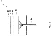
- FIG. 3 is an explanatory view for explaining a configuration of ultrasound probe 20.
- Ultrasound probe 20 includes protective layer 21, pMUT element 22 as an ultrasonic transmission/reception transducer, backing material 23, and signal processing circuit 24. Note that the detailed descriptions of pMUT element 22 will be given below.
- Protective layer 21 protects pMUT element 22.
- This protective layer 21 is formed from a comparatively flexible material such as silicone rubber or the like which, when coming into contact with a human body, does not give discomfort to the human body, and which has an acoustic impedance comparatively similar to that of the human body.
- Backing material 23 forms through-wiring for attenuating unnecessary vibration arising at pMUT element 22 and for electrically connecting pMUT element 22 to signal processing circuit 24. Additionally, backing material 23 has a function of transferring and diffusing, via signal processing circuit 24 through cable 30, heat arising at pMUT element 22, so as to prevent a temperature rise at the surface of the human body with which protective layer 21 comes into contact.
- Signal processing circuit 24 is a circuit which generates pulse signals for ultrasonic transmission, processes received pulse signals, and the like, and which is connected to ultrasound-diagnostic-apparatus body 10 via cable 30.
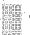
- PMUT element 22 is produced using Micro Electro Mechanical Systems (MEMS) techniques. PMUT element 22 is formed by bonding together substrate 101 in which multiple diaphragms 22a as vibrators are disposed two-dimensionally (or, one-dimensionally) and substrate 401 (see FIG. 5 described below) in which signal detection circuit 400 configured to detect signals from diaphragms 22a is provided.
- FIG. 4 is a plan view of substrate 101 for explaining diaphragms 22a. Diaphragms 22a transmit/receive ultrasonic waves by vibration. In FIG. 4 , the section surrounded by the dotted line (region E in FIG. 4 ) corresponds to one cell.
- FIG. 5 is a sectional view of one of diaphragms 22a constituting pMUT element 22.
- Diaphragm 22a is composed of piezoelectric element 100, and includes substrate 101 having opening 101d, vibrating plate 102, piezoelectric material layer 103, and electrodes 104a and 104b.
- Substrate 101 is a Silicon on Insulator (SOI) substrate formed by stacking, for example, Si layer 101a, SiO 2 layer 101b, and Si layer 101c on one another.
- Substrate 101 is an example of the MEMS substrate of the present invention.
- Vibrating plate 102 is formed by opening 101d provided by removing Si layer 101c and SiO 2 layer 101b, for example, by etching from the undersurface side of substrate 101. That is, vibrating plate 102 has a thin plate structure formed by Si layer 101a and opening 101d.
- Piezoelectric material layer 103 is composed of a thin film of PZT (lead zirconate titanate), for example, and is formed on the side opposite to opening 101d relative to vibrating plate 102 in order for vibrating plate 102 to be vibrated by an applied electric field.
- Piezoelectric material layer 103 is patterned and, for example, has a substantially regular octagonal cell shape in cross section. Note that, the cross section of piezoelectric material layer 103 may also have a shape other than regular octagonal (e.g., a circular shape, polygonal shape other than regular octagonal, or the like).
- Electrode 104a is an electrode on the side of upper surface of piezoelectric material layer 103, and is a common electrode.
- electrode 104b is an electrode on the side of undersurface of piezoelectric material layer 103, and is drawn out downward from substrate 101 via a through-silicon via or the like.
- Drawn-out electrode 104b is electrically connected to signal detection circuit 400 disposed on substrate 401.
- Signal detection circuit 400 is a CMOS circuit for detecting signals from diaphragms 22a, for example.
- Substrate 401 is an example of an electronic circuit substrate of the present invention.
- Signal detection circuit 400 is electrically connected to signal processing circuit 24.
- Diaphragms 22a are each designed such that the effectual acoustic impedance is consistent with the acoustic impedance of the living body, and thus can convey an ultrasonic wave to a living body efficiently.
- the rigidity of each of diaphragms 22a may be optimized, and more preferably, the material and thickness of vibrating plate 102, the thickness of piezoelectric material layer 103, the diameter of diaphragm 22a, the space between electrodes 104a and 104b, and/or the like may be optimized appropriately depending on a resonance frequency, transmission characteristics (sensitivity, frequency band), reception characteristics (sensitivity, frequency band), and/or the like.
- a SOI wafer having the stack structure in which SiO 2 layer 101b is stacked between two Si layers 101a and 101c is prepared as substrate 101, and electrode 104b is formed on a platelike silicon member on one side of substrate 101 by depositing titanium, gold, platinum, and the like by sputtering or the like.
- Piezoelectric material layer 103 is formed on electrode 104b by depositing PZT by sputtering process, sol-gel process, or the like. Additionally, electrode 104a is formed on piezoelectric material layer 103 by depositing gold, platinum, and the like by sputtering or the like.
- electrode 104a, piezoelectric material layer 103, and electrode 104b are shaped one after another by patterning such that electrode 104a, piezoelectric material layer 103, and electrode 104b each have substantially regular octagonal cell shapes. Additionally, openings 101d are each formed at a position corresponding to vibrating plate 102 in the platelike member by etching or the like from the surface of substrate 101 facing away from vibrating plate 102 and piezoelectric material layer 103. Each of these cell shapes corresponds to diaphragm 22a.
- electrode 104a, piezoelectric material layer 103, electrode 104b, and the platelike silicon member that is a part of substrate 101 are stacked on one another, and multiple vibrating plates 102 uncovered on the undersurface side of the stack are formed.
- electrode 104b on the lower side of piezoelectric material layer 103 is drawn out by the through-silicon via through substrate 101.
- Substrate 101 in which multiple diaphragms 22a are formed as described above is bonded to substrate 401 on which signal detection circuit (CMOS circuit) 400 is formed in advance after substrate 101 is aligned to substrate 400.
- CMOS circuit signal detection circuit
- flip chip assembly techniques such as an anisotropic conductive film (ACF), solder bump, and/or the like may be used, for example. Both of the electrodes are connected to signal detection circuit 400 at this time. The details of the alignment method will be described below.
- diaphragms 22a of pMUT element 22 are produced by forming piezoelectric material layer 103 on one surface of substrate 101 that is a SOI substrate and thereafter by providing openings 101d in the other surface by etching to form vibrating plates 102.
- an etching solution may flow comparatively more into places near the edge portion of the SOI wafer as substrate 101 than into a place near the central portion, so that the etching rate may increase in such places near the edge portion.
- variations in characteristics between those of diaphragms 22a formed near the central portion and those of diaphragms 22a formed near the edge portion of substrate 101 may arise.
- diaphragms 22a when arise, make preferable transmission/reception of ultrasonic waves difficult. In order to avoid such a situation, some of produced multiple diaphragms 22a are determined as dummy diaphragms and are not used for the transmission/reception of ultrasonic waves in the embodiments of the present invention.
- FIG. 6 is an explanatory view for explaining channel diaphragms 22aC constituting a channel for transmission/reception of ultrasonic waves, and for explaining dummy diaphragms 22aD.
- those of two-dimensionally disposed diaphragms 22a disposed in predetermined numbers of columns and rows (two columns and two rows in FIG. 6 ) from the farthest edge portion are determined as dummy diaphragms 22aD
- those of two-dimensionally disposed diaphragms 22a disposed inside dummy diaphragms 22aD are determined as channel diaphragms 22aC.
- the solid line corresponds to the edge of substrate 101 in FIG. 6 .
- channel diaphragms 22aC and dummy diaphragms 22aD there is no difference between methods for producing channel diaphragms 22aC and dummy diaphragms 22aD, and their structures are the same at the design stage.
- those of diaphragms 22a which are disposed at the position where the variations in characteristics arise at the production stage (during etching), for example, at the position near the edge portion are dummy diaphragms 22aD.
- Dummy diaphragms 22aD are not used for transmission/reception of ultrasonic waves, and are not connected to signal detection circuit 400.
- dummy diaphragms 22aD may be configured not to include the aforementioned through-silicon vias from electrodes 104b, for example.
- dummy diaphragms 22aD which are not used for transmission/reception of ultrasonic waves, so that the characteristics of pMUT element 22 as the ultrasonic transmission/reception transducer can be made preferable.
- diaphragms 22a formed near the edge portion are determined as dummy diaphragms 22aD in the example illustrated in FIG. 6 , the present invention is not limited to this example and those of diaphragms 22a disposed at other positions may also be determined as dummy diaphragms 22aD.
- Substrate 101 in which multiple diaphragms 22a are formed by the aforementioned production method is aligned to substrate 401 on which signal detection circuit 400 is formed, and thereafter substrates 101 and 401 are bonded to each other.
- the method for aligning substrate 101 to substrate 401 will be described.
- FIG. 7A is an explanatory view for explaining an alignment diaphragm
- FIG. 7B is a plan view of substrate 401 for explaining alignment mark 402.
- illustration of signal detection circuit 400 formed on substrate 401 is omitted.
- FIG. 7A illustrates at least one of multiple dummy diaphragms 22aD.
- dummy diaphragm 22aD used for alignment is referred to as “alignment diaphragm 22aP.”
- FIG. 7A illustrates the case where those of diaphragms 22a which are disposed in predetermined columns and rows near the edge portion of substrate 101 are determined as dummy diaphragms 22aD.
- Method 1 vibrating plate 102, piezoelectric material layer 103, and electrodes 104a and 104b constituting alignment diaphragm 22aP are broken up and removed, and observation window OW is created.
- This breaking-up and removal are carried out, for example, immediately before substrate 101 and substrate 401 are aligned to each other.
- Breaking-up and removal of alignment diaphragm 22aP may be carried out by breaking up and removing vibrating plate 102, piezoelectric material layer 103, and electrodes 104a and 104b constituting alignment diaphragm 22aP, for example, using a stick or the like having a diameter smaller than that of dummy diaphragm 22aD.
- observation window OW is a mere hole having the same size and shape as other diaphragms 22a.
- vibrating plate 102, piezoelectric material layer 103, and electrodes 104a and 104b are each a thin film having a thickness of the order of ⁇ m, and therefore, breaking-up of alignment diaphragm 22aP can be easily done only by lightly touching with the aforementioned stick or the like.
- alignment mark 402 is provided at a position of substrate 401 corresponding to observation window OW of substrate 101.
- Alignment mark 402 is an example of an alignment item of the present invention.
- alignment mark 105 of the same shape and of the same direction as alignment mark 402 provided on substrate 401 illustrated in FIG. 7B is provided on substrate 101 in advance.
- methods for forming alignment marks 105 and 402 include a sputtering process, vapor deposition process, pattern printing process, and the like.
- FIG. 8 is an explanatory view for explaining alignment method 1 and is a sectional view of substrates 101 and 401 at the position of alignment diaphragm 22aP. Note that, illustration of diaphragms 22a other than alignment diaphragm 22aP is omitted in FIG. 8 for explanation.
- the optical recognition device moves substrate 101 or substrate 401 until the shape and direction of alignment mark 402 recognized through observation window OW and the shape and direction of alignment mark 105 provided on substrate 101 correspond to each other in pattern matching. This allows accurate alignment between substrates 101 and 401.
- observation windows OW and alignment marks 402 are not particularly limited in the embodiments of the present invention, it is desirable to provide at least two or more observation windows OW and alignment marks 402 on each of substrates 101 and 401 from a viewpoint of alignment between substrates. More preferably, it is desirable to provide observation windows OW and alignment marks 402 at positions of each of substrates 101 and 401 corresponding to dummy diaphragms 22aD existing on opposite sides of the edge portion of substrate 101 across the center of substrate 101. Still more preferably, observation windows OW and alignment marks 402 may also be provided at positions corresponding to four dummy diaphragms 22aD existing on two mutually perpendicular lines among multiple lines passing through the center.
- alignment mark 105 used for pattern matching is provided on substrate 101 in aforementioned Method 1, Method 2 described below will be described in relation to the case where alignment mark 105 is not provided on substrate 101.
- substrates 101 and 401 for which the alignment is accomplished are prepared, and the shape of alignment mark 402 recognized through observation window OW in the case where substrates 101 and 401 are successfully aligned to each other (such a shape may hereinafter be referred to as "first shape") is stored in advance in the optical recognition device. Then, when substrates 101 and 401 are actually aligned to each other, the optical recognition device moves substrate 101 or substrate 401 until the shape of alignment mark 402 recognized through observation window OW corresponds to the first shape stored in advance. This allows accurate alignment between substrates 101 and 401.
- alignment mark 402 not only the shape of alignment mark 402 but also the shape of inner wall surface of observation window OW and the shape of alignment mark 402 recognized through observation window OW may also be stored together in the optical recognition device in advance as the aforementioned first shape.
- vibrating plate 102 that is one component element of diaphragm 22a has the thin plate structure composed of the Si layer. It has been understood that silicon thin films transmit infrared radiation.
- the optical recognition device can use the infrared radiation for recognition of alignment mark 402 so as to perform alignment without breaking up alignment diaphragm 22aP.
- FIG. 9 is an explanatory view for explaining alignment method 3 in which infrared light is used.
- piezoelectric material layer 103 and electrodes 104a and 104b prevent transmission of infrared radiation, it is desirable to remove piezoelectric material layer 103 and electrodes 104a and 104b by etching or the like before the alignment process.
- Method 4 is a method in which scribe lines used during chip separation are utilized.
- Substrate 101 that is a SOI substrate includes predetermined scribe lines.
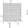
- alignment diaphragm 22aP is provided on any of these scribe lines.
- FIG. 10 is an explanatory view for explaining a case where alignment diaphragm 22aP is provided on one of scribe lines SL.
- observation window OW is created as with Method 1 by removing a remainder of alignment diaphragm 22aP, and the optical recognition device recognizes the shape of alignment mark 402 on substrate 401 through observation window OW, so that alignment may be performed by pattern matching with alignment mark 105 provided on substrate 101. Additionally or alternatively, the alignment may also be performed based on the shape of side wall surface left after removal of alignment diaphragm 22aP (the shape of side wall surface of observation window OW) and based on the shape of alignment mark 402 recognized through observation window OW. Additionally or alternatively, the alignment may also be performed by providing an alignment mark in the side surface of substrate 101 during scribing and by using the alignment mark.
- the method for producing a MEMS transducer includes: a step of producing substrate 101 (corresponding to the MEMS substrate of the present invention) by using a MEMS technique to form multiple diaphragms 22a in a substrate, multiple diaphragms 22a being formed by forming piezoelectric material layer 103 on one surface of the substrate and thereafter by forming openings 101d in the substrate from the other surface of the substrate; a step of aligning substrate 101 to substrate 401 on which signal detection circuit 400 is formed (substrate 401 corresponds to the electronic circuit substrate of the present invention), by using at least one of multiple diaphragms 22a as alignment diaphragm 22aP; and a step of bonding together substrate 101 and substrate 401.
- substrate 101 is aligned to substrate 401 by using a part of multiple diaphragms 22a formed on substrate 101 as alignment diaphragm 22aP. This allows highly accurate alignment using a common optical recognition device or the like neither without an additional process nor without highly accurate equipment for alignment.
- a structure for alignment is provided not on the side of substrate 401 that is the electronic circuit substrate side but on the side of substrate 101 that is the MEMS substrate side, so that it is preferable in view of the cost that the same circuit can be used as the electronic circuit substrate when the MEMS transducer in which the MEMS substrate including various characteristics and the electronic circuit substrate are bonded together is produced. From the above reasoning, substrate 101 that is the MEMS substrate and substrate 401 that is the electronic circuit substrate can be connected to each other with high accuracy and ta low cost.
- alignment using the method for producing a MEMS transducer according to the embodiments of the present invention brings about the following advantages.
- upper and lower electrodes (electrodes 104a and 104b) and piezoelectric substance material layer 103 can be processed from the front surface using the alignment mark existing on the same front surface.
- opening 101d it is necessary to perform backside alignment from the back surface based on the alignment mark on the front surface and to process from the back surface, so that the position of piezoelectric material layer 103 may be shifted slightly from the position of opening 101d depending on the accuracy.
- multiple diaphragms 22a include channel diaphragms 22aC which constitute the channel used for transmission/reception of ultrasonic waves (channel diaphragms 22aC correspond to the first diaphragms of the present invention) and dummy diaphragms 22aD not used for transmission/reception of ultrasonic waves (dummy diaphragms 22aD correspond to the second diaphragms of the present invention), and alignment diaphragm 22aP is at least one of dummy diaphragms 22aD.
- alignment diaphragm 22aP can be formed simultaneously in the same processing process as the normal channel diaphragms 22aC, so that high relative-position accuracy can be ensured and the cost can be held down.
- the method for producing of a MEMS transducer further includes a step of creating observation window OW by destroying and removing alignment diaphragm 22aP, and, in the step of aligning substrate 101 to substrate 401, substrates 101 and 401 are aligned to each other based on observation window OW and alignment mark 402 provided on substrate 401 in advance (alignment mark 402 corresponds to the alignment item of the present invention).
- the method for producing of a MEMS transducer further includes a step of removing piezoelectric material layer 103 located on alignment diaphragm 22aP, and, in the step of bonding together substrates 101 and 401, substrates 101 and 401 are aligned to each other based on alignment diaphragm 22aP and alignment mark 402 provided on substrate 401 in advance, using infrared radiation that passes through alignment diaphragm 22aP from which piezoelectric material layer 103 is removed.
- the method for producing of a MEMS transducer further includes a step of forming alignment diaphragm 22aP, in the step of producing substrate 101, on scribe line SL used for singulation of substrate 101, and, in the step of bonding together substrates 101 and 401, substrates 101 and 401 are aligned to each other based on alignment diaphragm 22aP and alignment mark 402 provided on substrate 401 in advance.
- substrate 101 that is the MEMS substrate and substrate 401 that is the electronic circuit substrate can be connected to each other with high accuracy and ta low cost.
- the pMUT that is an ultrasonic transducer has been described as an example of the MEMS transducer.
- the present invention is not limited to this example.
- the present invention is widely applicable to various kinds of piezoelectric modules (and piezoelectric devices using the piezoelectric modules), each of which includes a diaphragm layer and a piezoelectric material layer disposed on the diaphragm layer and utilizes converting function of converting mechanical deformation of a piezoelectric substance to voltage.
- the present invention may also be applied, for example, to an angular velocity sensor, an inkjet head, a minute-mirrors actuating element, or the like.
- the present invention is suitable for a method for producing a MEMS transducer used for an ultrasound diagnostic apparatus..
Landscapes
- Engineering & Computer Science (AREA)
- Health & Medical Sciences (AREA)
- Life Sciences & Earth Sciences (AREA)
- Microelectronics & Electronic Packaging (AREA)
- Mechanical Engineering (AREA)
- Pathology (AREA)
- Physics & Mathematics (AREA)
- General Health & Medical Sciences (AREA)
- Surgery (AREA)
- Biomedical Technology (AREA)
- Heart & Thoracic Surgery (AREA)
- Medical Informatics (AREA)
- Molecular Biology (AREA)
- Nuclear Medicine, Radiotherapy & Molecular Imaging (AREA)
- Animal Behavior & Ethology (AREA)
- Biophysics (AREA)
- Public Health (AREA)
- Veterinary Medicine (AREA)
- Radiology & Medical Imaging (AREA)
- Manufacturing & Machinery (AREA)
- Chemical & Material Sciences (AREA)
- Ceramic Engineering (AREA)
- Computer Vision & Pattern Recognition (AREA)
- Computer Hardware Design (AREA)
- Gynecology & Obstetrics (AREA)
- Analytical Chemistry (AREA)
- Biochemistry (AREA)
- General Physics & Mathematics (AREA)
- Immunology (AREA)
- Ultra Sonic Daignosis Equipment (AREA)
- Transducers For Ultrasonic Waves (AREA)
Abstract
Description
- The present invention relates to a method for producing a MEMS transducer used for transmission/reception of ultrasonic waves, a MEMS transducer, an ultrasound probe, and an ultrasound diagnostic apparatus.
- Micro electro mechanical system (MEMS) devices produced by MEMS techniques using semiconductor manufacturing techniques have spread recently. The MEMS devices are used for sensors, transducers, and the like.
- Examples of those of the transducers which are configured to generate ultrasonic waves (ultrasound transducers) include a piezoelectric micromachined ultrasonic transducer (pMUT). The pMUT transmits/receives ultrasonic waves by causing vibration of a diaphragm (movable film) in the same manner as a drum. The diaphragm has a unimorph structure in which a piezoelectric thin film (actuator layer) such as PTZ is formed on a substrate (base material layer) such as a silicon substrate or the like.
- As compared, for example, with piezoelectric elements divided by dicing or the like of a bulk PTZ, the pMUT has various characteristics as follows: a frequency bandwidth can be wider; further micromachining is possible, so that high-resolution can be expected; the pMUT is suitable for forming a two-dimensional array of piezoelectric elements for generating three-dimensional images; miniaturization and thickness reduction is possible; and the like.
- Examples of semiconductor manufacturing methods using MEMS techniques include techniques disclosed in Japanese Patent No.
5108100 5450396 2006-202918 - Such a pMUT is produced by bonding together a substrate (MEMS substrate) in which diaphragms are formed, another substrate (electronic circuit substrate) on which a signal detection circuit (e.g., CMOS circuit) adapted to detect transmission/reception signals for transmission/reception of ultrasonic waves at the diaphragms is formed, interposer, and connecting wiring such as a flexible wiring board or the like.
- In this respect, when it is attempted to produce the pMUT by forming the MEMS substrate and electronic substrate at the same time (i.e., by forming the MEMS substrate on the electronic circuit substrate on which the signal detection circuit has been formed, for example), the following disadvantages are caused. That is, high temperature annealing is required in order to deposit a preferable piezoelectric thin film (for example, PZT) on the MEMS substrate, so that the signal detection circuit may be damaged by the high temperature. Additionally, when the MEMS substrate is formed on the signal detection circuit of the electronic circuit substrate, the signal detection circuit of the same size as the MEMS substrate needs to be prepared and this necessity causes a disadvantage in terms of yield of the signal detection circuit. Accordingly, it is desirable for the MEMS substrate and the electronic circuit substrate to be manufactured individually and then bonded together.
- When the MEMS substrate and the electronic circuit substrate are manufactured individually and then bonded together, highly accurate alignment in bonding is required for achieving a higher-definition and higher-resolution ultrasound diagnostic apparatus. However, for achieving highly accurate alignment, dedicated equipment for highly mechanically accurate alignment and/or additional machining for alignment are required, which cost greatly. Moreover, there has been a problem of low accuracy due to inability to directly observe connected surfaces when bonding together the MEMS substrate and the electronic circuit substrate. Thus, in cases where high-density and multi-pin connection is required as in the case of ultrasonic transducers, there has been a risk of a connection error being caused.
- Additionally, there has been a demand for different ultrasound probes (e.g., linear type, convex type, sector type, and the like) to be properly used, and similarly, there also has been a demand for multiple MEMS substrates of different sizes and shapes to be prepared in advance and to be properly used according to observation targets during ultrasonic diagnosis using an ultrasound diagnostic apparatus. In contrast, as for the electronic circuit substrate, it is preferable in view of the cost that the same circuit can possibly be used. For the reasons as stated above, it is desirable for the MEMS substrate to mainly include alignment means.
- Thus, there is a demand for a technique making it possible to connect the MEMS substrate and the electronic circuit substrate with high accuracy and at low cost.
- Objects of the present invention are to provide a method for producing of a MEMS transducer, in which a MEMS substrate and an electronic circuit substrate can be connected with high accuracy and at low cost, a MEMS transducer, an ultrasound probe, and an ultrasound diagnostic apparatus.
- In order to achieve at least one of the aforementioned objects, the method for producing of the MEMS transducer, in which one aspect of the present invention is reflected, includes: a step of producing a MEMS substrate by using a MEMS technique to form a plurality of diaphragms in a substrate, the plurality of diaphragms being formed by forming a piezoelectric material layer on one surface of the substrate and thereafter by forming openings in the substrate from the other surface of the substrate; a step of performing alignment between the MEMS substrate and an electronic circuit substrate by using at least one of the plurality of diaphragms as an alignment diaphragm; and a step of bonding together the MEMS substrate and the electronic circuit substrate.
- The advantages and features provided by one or more embodiments of the invention will become more fully understood from the detailed description given hereinbelow and the appended drawings which are given by way of illustration only, and thus are not intended as a definition of the limits of the present invention:
-
FIG. 1 illustrates a configuration in external appearance of an ultrasound diagnostic apparatus including an ultrasonic transducer; -
FIG. 2 is a block diagram illustrating an electrical configuration example of the ultrasound diagnostic apparatus; -
FIG. 3 is an explanatory view for explaining a configuration of an ultrasound probe; -
FIG. 4 is a plan view of a substrate for explaining diaphragms; -
FIG. 5 is a sectional view of one of the diaphragms constituting a pMUT element; -
FIG. 6 is an explanatory view for explaining channel diaphragms constituting a channel for transmission/reception of ultrasonic waves, and for explaining dummy diaphragms; -
FIG. 7A is an explanatory view for explaining an alignment diaphragm; -
FIG. 7B is a plan view of the substrate for explaining an alignment mark; -
FIG. 8 is an explanatory view for explainingalignment method 1; -
FIG. 9 is an explanatory view for explaining alignment method 3 in which infrared light is used; and -
FIG. 10 is an explanatory view for explaining a case where the alignment diaphragm is provided on one of scribe lines SL. - Hereinafter, one or more embodiments of the present invention will be described with reference to the drawings. However, the scope of the invention is not limited to the disclosed embodiments.
-
FIG. 1 illustrates a configuration of an ultrasound diagnostic apparatus in external appearance, the ultrasound diagnostic apparatus including an ultrasonic transducer as an example of a MEMS transducer according to embodiments of the present invention.FIG. 2 is a block diagram illustrating an electrical configuration example of the ultrasound diagnostic apparatus according to the embodiments of the present invention. - Ultrasound
diagnostic apparatus 1 is configured to include ultrasound-diagnostic-apparatus body 10,ultrasound probe 20, andcable 30. -
Ultrasound probe 20 transmits ultrasonic signals to a human body as a subject (not illustrated), and receives the ultrasonic signals reflected by the human body. Inultrasound probe 20, multiple pMUT cells (described hereinbelow) that are ultrasonic transducers are arranged. - Ultrasound-diagnostic-
apparatus body 10 is connected toultrasound probe 20 viacable 30, and transmits transmission signals that are electrical signals viacable 30, so as to allowultrasound probe 20 to transmit the ultrasonic signals. Additionally, ultrasound-diagnostic-apparatus body 10 forms ultrasonographic images of the internal state of the human body using electrical signals generated atultrasound probe 20 based on the ultrasonic signals received byultrasound probe 20. - Specifically, ultrasound-diagnostic-
apparatus body 10 is configured to includeoperation input section 11,transmission section 12,reception section 13,image processing section 14,display section 15, andcontrol section 16. - For example, a command indicating the start of diagnosis, information on a subject, or the like are input using
operation input section 11.Operation input section 11 is an operation panel, a keyboard, or the like provided with multiple input switches, for example. -
Transmission section 12 transmits control signals received fromcontrol section 16 toultrasound probe 20 viacable 30. That is,transmission section 12 makesultrasound probe 20 operate for transmission of ultrasonic signals to the subject. -
Reception section 13 receives viacable 30, reception signals transmitted fromultrasound probe 20. That is,reception section 13 makesultrasound probe 20 operate to receive ultrasonic signals coming from the subject in response to the transmitted ultrasonic signals. Then,reception section 13 outputs the received ultrasonic signals toimage processing section 14. -
Image processing section 14 uses the ultrasonic signals received fromreception section 13 to generate an image (ultrasonographic image) for ultrasonic diagnosis in accordance with instructions bycontrol section 16. The ultrasonographic image shows the internal state of the subject. -
Display section 15 displays the ultrasonographic image generated byimage processing section 14 in accordance with instructions bycontrol section 16. -
Control section 16 controlsoperation input section 11,transmission section 12,reception section 13,image processing section 14, anddisplay section 15 according to their functions, so as to entirely control ultrasounddiagnostic apparatus 1. -
FIG. 3 is an explanatory view for explaining a configuration ofultrasound probe 20.Ultrasound probe 20 includesprotective layer 21,pMUT element 22 as an ultrasonic transmission/reception transducer, backingmaterial 23, andsignal processing circuit 24. Note that the detailed descriptions ofpMUT element 22 will be given below. -
Protective layer 21 protectspMUT element 22. Thisprotective layer 21 is formed from a comparatively flexible material such as silicone rubber or the like which, when coming into contact with a human body, does not give discomfort to the human body, and which has an acoustic impedance comparatively similar to that of the human body. - Backing
material 23 forms through-wiring for attenuating unnecessary vibration arising atpMUT element 22 and for electrically connectingpMUT element 22 to signalprocessing circuit 24. Additionally, backingmaterial 23 has a function of transferring and diffusing, viasignal processing circuit 24 throughcable 30, heat arising atpMUT element 22, so as to prevent a temperature rise at the surface of the human body with whichprotective layer 21 comes into contact.Signal processing circuit 24 is a circuit which generates pulse signals for ultrasonic transmission, processes received pulse signals, and the like, and which is connected to ultrasound-diagnostic-apparatus body 10 viacable 30. -
PMUT element 22 is produced using Micro Electro Mechanical Systems (MEMS) techniques.PMUT element 22 is formed by bonding togethersubstrate 101 in whichmultiple diaphragms 22a as vibrators are disposed two-dimensionally (or, one-dimensionally) and substrate 401 (seeFIG. 5 described below) in which signaldetection circuit 400 configured to detect signals fromdiaphragms 22a is provided.FIG. 4 is a plan view ofsubstrate 101 for explainingdiaphragms 22a.Diaphragms 22a transmit/receive ultrasonic waves by vibration. InFIG. 4 , the section surrounded by the dotted line (region E inFIG. 4 ) corresponds to one cell. -
FIG. 5 is a sectional view of one ofdiaphragms 22a constitutingpMUT element 22.Diaphragm 22a is composed ofpiezoelectric element 100, and includessubstrate 101 havingopening 101d, vibratingplate 102,piezoelectric material layer 103, andelectrodes -
Substrate 101 is a Silicon on Insulator (SOI) substrate formed by stacking, for example,Si layer 101a, SiO2 layer 101b, andSi layer 101c on one another.Substrate 101 is an example of the MEMS substrate of the present invention. Vibratingplate 102 is formed by opening 101d provided by removingSi layer 101c and SiO2 layer 101b, for example, by etching from the undersurface side ofsubstrate 101. That is, vibratingplate 102 has a thin plate structure formed bySi layer 101a andopening 101d. -
Piezoelectric material layer 103 is composed of a thin film of PZT (lead zirconate titanate), for example, and is formed on the side opposite to opening 101d relative to vibratingplate 102 in order for vibratingplate 102 to be vibrated by an applied electric field.Piezoelectric material layer 103 is patterned and, for example, has a substantially regular octagonal cell shape in cross section. Note that, the cross section ofpiezoelectric material layer 103 may also have a shape other than regular octagonal (e.g., a circular shape, polygonal shape other than regular octagonal, or the like). -
Electrode 104a is an electrode on the side of upper surface ofpiezoelectric material layer 103, and is a common electrode. In contrast,electrode 104b is an electrode on the side of undersurface ofpiezoelectric material layer 103, and is drawn out downward fromsubstrate 101 via a through-silicon via or the like. - Drawn-
out electrode 104b is electrically connected to signaldetection circuit 400 disposed onsubstrate 401.Signal detection circuit 400 is a CMOS circuit for detecting signals fromdiaphragms 22a, for example.Substrate 401 is an example of an electronic circuit substrate of the present invention.Signal detection circuit 400 is electrically connected to signalprocessing circuit 24. -
Diaphragms 22a are each designed such that the effectual acoustic impedance is consistent with the acoustic impedance of the living body, and thus can convey an ultrasonic wave to a living body efficiently. Specifically, the rigidity of each ofdiaphragms 22a may be optimized, and more preferably, the material and thickness of vibratingplate 102, the thickness ofpiezoelectric material layer 103, the diameter ofdiaphragm 22a, the space betweenelectrodes - Next, the method for producing
pMUT element 22 configured as described above will be described. - To begin with, a SOI wafer having the stack structure in which SiO2 layer 101b is stacked between two
Si layers substrate 101, andelectrode 104b is formed on a platelike silicon member on one side ofsubstrate 101 by depositing titanium, gold, platinum, and the like by sputtering or the like. -
Piezoelectric material layer 103 is formed onelectrode 104b by depositing PZT by sputtering process, sol-gel process, or the like. Additionally,electrode 104a is formed onpiezoelectric material layer 103 by depositing gold, platinum, and the like by sputtering or the like. - Next,
electrode 104a,piezoelectric material layer 103, andelectrode 104b are shaped one after another by patterning such thatelectrode 104a,piezoelectric material layer 103, andelectrode 104b each have substantially regular octagonal cell shapes. Additionally,openings 101d are each formed at a position corresponding to vibratingplate 102 in the platelike member by etching or the like from the surface ofsubstrate 101 facing away from vibratingplate 102 andpiezoelectric material layer 103. Each of these cell shapes corresponds todiaphragm 22a. - In this way, electrode 104a,
piezoelectric material layer 103,electrode 104b, and the platelike silicon member that is a part ofsubstrate 101 are stacked on one another, and multiple vibratingplates 102 uncovered on the undersurface side of the stack are formed. - Then,
electrode 104b on the lower side ofpiezoelectric material layer 103 is drawn out by the through-silicon via throughsubstrate 101. -
Substrate 101 in whichmultiple diaphragms 22a are formed as described above is bonded tosubstrate 401 on which signal detection circuit (CMOS circuit) 400 is formed in advance aftersubstrate 101 is aligned tosubstrate 400. As for the bonding method, flip chip assembly techniques, such as an anisotropic conductive film (ACF), solder bump, and/or the like may be used, for example. Both of the electrodes are connected to signaldetection circuit 400 at this time. The details of the alignment method will be described below. - As described above,
diaphragms 22a ofpMUT element 22 are produced by formingpiezoelectric material layer 103 on one surface ofsubstrate 101 that is a SOI substrate and thereafter by providingopenings 101d in the other surface by etching to form vibratingplates 102. - It should be noted that, when
multiple diaphragms 22a are formed insubstrate 101 by the method as described above, an etching solution may flow comparatively more into places near the edge portion of the SOI wafer assubstrate 101 than into a place near the central portion, so that the etching rate may increase in such places near the edge portion. In that case, variations in characteristics between those ofdiaphragms 22a formed near the central portion and those ofdiaphragms 22a formed near the edge portion ofsubstrate 101 may arise. - The variations in characteristics of
diaphragms 22a, when arise, make preferable transmission/reception of ultrasonic waves difficult. In order to avoid such a situation, some of producedmultiple diaphragms 22a are determined as dummy diaphragms and are not used for the transmission/reception of ultrasonic waves in the embodiments of the present invention. -
FIG. 6 is an explanatory view for explaining channel diaphragms 22aC constituting a channel for transmission/reception of ultrasonic waves, and for explaining dummy diaphragms 22aD. In the example illustrated inFIG. 6 , those of two-dimensionallydisposed diaphragms 22a disposed in predetermined numbers of columns and rows (two columns and two rows inFIG. 6 ) from the farthest edge portion are determined as dummy diaphragms 22aD, and those of two-dimensionallydisposed diaphragms 22a disposed inside dummy diaphragms 22aD are determined as channel diaphragms 22aC. Note that the solid line corresponds to the edge ofsubstrate 101 inFIG. 6 . - There is no difference between methods for producing channel diaphragms 22aC and dummy diaphragms 22aD, and their structures are the same at the design stage. In the example illustrated in
FIG. 6 , those ofdiaphragms 22a which are disposed at the position where the variations in characteristics arise at the production stage (during etching), for example, at the position near the edge portion are dummy diaphragms 22aD. Dummy diaphragms 22aD are not used for transmission/reception of ultrasonic waves, and are not connected to signaldetection circuit 400. Specifically, dummy diaphragms 22aD may be configured not to include the aforementioned through-silicon vias fromelectrodes 104b, for example. - In this way, some of
multiple diaphragms 22a produced by the same production method are determined as dummy diaphragms 22aD which are not used for transmission/reception of ultrasonic waves, so that the characteristics ofpMUT element 22 as the ultrasonic transmission/reception transducer can be made preferable. Note that, although those ofdiaphragms 22a formed near the edge portion are determined as dummy diaphragms 22aD in the example illustrated inFIG. 6 , the present invention is not limited to this example and those ofdiaphragms 22a disposed at other positions may also be determined as dummy diaphragms 22aD. -
Substrate 101 in whichmultiple diaphragms 22a are formed by the aforementioned production method is aligned tosubstrate 401 on whichsignal detection circuit 400 is formed, and thereaftersubstrates substrate 101 tosubstrate 401 will be described. -
FIG. 7A is an explanatory view for explaining an alignment diaphragm, andFIG. 7B is a plan view ofsubstrate 401 for explainingalignment mark 402. InFIG. 7B , illustration ofsignal detection circuit 400 formed onsubstrate 401 is omitted. - As illustrated in
FIG. 7A , at least one of multiple dummy diaphragms 22aD is used for alignment. Hereinbelow, dummy diaphragm 22aD used for alignment is referred to as "alignment diaphragm 22aP." Note that, as in the illustration ofFIG. 6 ,FIG. 7A illustrates the case where those ofdiaphragms 22a which are disposed in predetermined columns and rows near the edge portion ofsubstrate 101 are determined as dummy diaphragms 22aD. - In
Method 1, vibratingplate 102,piezoelectric material layer 103, andelectrodes substrate 101 andsubstrate 401 are aligned to each other. Breaking-up and removal of alignment diaphragm 22aP may be carried out by breaking up and removing vibratingplate 102,piezoelectric material layer 103, andelectrodes Method 1, observation window OW is a mere hole having the same size and shape asother diaphragms 22a. Note that, vibratingplate 102,piezoelectric material layer 103, andelectrodes - As illustrated in
FIG. 7B ,alignment mark 402 is provided at a position ofsubstrate 401 corresponding to observation window OW ofsubstrate 101.Alignment mark 402 is an example of an alignment item of the present invention. - Moreover, as illustrated in
FIG. 7A ,alignment mark 105 of the same shape and of the same direction asalignment mark 402 provided onsubstrate 401 illustrated inFIG. 7B is provided onsubstrate 101 in advance. Note that examples of methods for forming alignment marks 105 and 402 include a sputtering process, vapor deposition process, pattern printing process, and the like. - The alignment and bonding of
substrates FIG. 8 , whilesubstrate 101 is held abovesubstrate 401,substrate 101 orsubstrate 401 is moved to a position wherealignment mark 402 provided onsubstrate 401 is preferably observed by a camera of the optical recognition device through observation window OW.FIG. 8 is an explanatory view for explainingalignment method 1 and is a sectional view ofsubstrates diaphragms 22a other than alignment diaphragm 22aP is omitted inFIG. 8 for explanation. - Here, the optical recognition device moves
substrate 101 orsubstrate 401 until the shape and direction ofalignment mark 402 recognized through observation window OW and the shape and direction ofalignment mark 105 provided onsubstrate 101 correspond to each other in pattern matching. This allows accurate alignment betweensubstrates - Note that, although the number and positions of observation windows OW and alignment marks 402 are not particularly limited in the embodiments of the present invention, it is desirable to provide at least two or more observation windows OW and alignment marks 402 on each of
substrates substrates substrate 101 across the center ofsubstrate 101. Still more preferably, observation windows OW and alignment marks 402 may also be provided at positions corresponding to four dummy diaphragms 22aD existing on two mutually perpendicular lines among multiple lines passing through the center. - Although
alignment mark 105 used for pattern matching is provided onsubstrate 101 inaforementioned Method 1, Method 2 described below will be described in relation to the case wherealignment mark 105 is not provided onsubstrate 101. - To begin with,
substrates alignment mark 402 recognized through observation window OW in the case wheresubstrates substrates substrate 101 orsubstrate 401 until the shape ofalignment mark 402 recognized through observation window OW corresponds to the first shape stored in advance. This allows accurate alignment betweensubstrates - Note that, not only the shape of
alignment mark 402 but also the shape of inner wall surface of observation window OW and the shape ofalignment mark 402 recognized through observation window OW may also be stored together in the optical recognition device in advance as the aforementioned first shape. - As described above, vibrating
plate 102 that is one component element ofdiaphragm 22a has the thin plate structure composed of the Si layer. It has been understood that silicon thin films transmit infrared radiation. The optical recognition device can use the infrared radiation for recognition ofalignment mark 402 so as to perform alignment without breaking up alignment diaphragm 22aP.FIG. 9 is an explanatory view for explaining alignment method 3 in which infrared light is used. - However, because
piezoelectric material layer 103 andelectrodes piezoelectric material layer 103 andelectrodes - Method 4 is a method in which scribe lines used during chip separation are utilized.
Substrate 101 that is a SOI substrate includes predetermined scribe lines. In Method 4, alignment diaphragm 22aP is provided on any of these scribe lines. -
FIG. 10 is an explanatory view for explaining a case where alignment diaphragm 22aP is provided on one of scribe lines SL. - In the case where alignment diaphragm 22aP is provided on one of scribe lines SL, observation window OW is created as with
Method 1 by removing a remainder of alignment diaphragm 22aP, and the optical recognition device recognizes the shape ofalignment mark 402 onsubstrate 401 through observation window OW, so that alignment may be performed by pattern matching withalignment mark 105 provided onsubstrate 101. Additionally or alternatively, the alignment may also be performed based on the shape of side wall surface left after removal of alignment diaphragm 22aP (the shape of side wall surface of observation window OW) and based on the shape ofalignment mark 402 recognized through observation window OW. Additionally or alternatively, the alignment may also be performed by providing an alignment mark in the side surface ofsubstrate 101 during scribing and by using the alignment mark. - As described above, the method for producing a MEMS transducer according to the embodiments of the present invention includes: a step of producing substrate 101 (corresponding to the MEMS substrate of the present invention) by using a MEMS technique to form
multiple diaphragms 22a in a substrate,multiple diaphragms 22a being formed by formingpiezoelectric material layer 103 on one surface of the substrate and thereafter by formingopenings 101d in the substrate from the other surface of the substrate; a step of aligningsubstrate 101 tosubstrate 401 on whichsignal detection circuit 400 is formed (substrate 401 corresponds to the electronic circuit substrate of the present invention), by using at least one ofmultiple diaphragms 22a as alignment diaphragm 22aP; and a step of bonding togethersubstrate 101 andsubstrate 401. - In this way, according to the method for producing the MEMS transducer according to the embodiments of the present invention,
substrate 101 is aligned tosubstrate 401 by using a part ofmultiple diaphragms 22a formed onsubstrate 101 as alignment diaphragm 22aP. This allows highly accurate alignment using a common optical recognition device or the like neither without an additional process nor without highly accurate equipment for alignment. Additionally, a structure for alignment (alignment diaphragm 22aP) is provided not on the side ofsubstrate 401 that is the electronic circuit substrate side but on the side ofsubstrate 101 that is the MEMS substrate side, so that it is preferable in view of the cost that the same circuit can be used as the electronic circuit substrate when the MEMS transducer in which the MEMS substrate including various characteristics and the electronic circuit substrate are bonded together is produced. From the above reasoning,substrate 101 that is the MEMS substrate andsubstrate 401 that is the electronic circuit substrate can be connected to each other with high accuracy and ta low cost. - Note that alignment using the method for producing a MEMS transducer according to the embodiments of the present invention brings about the following advantages. When each of
diaphragms 22a is formed insubstrate 101, upper and lower electrodes (electrodes substance material layer 103 can be processed from the front surface using the alignment mark existing on the same front surface. In contrast, when opening 101d is formed, it is necessary to perform backside alignment from the back surface based on the alignment mark on the front surface and to process from the back surface, so that the position ofpiezoelectric material layer 103 may be shifted slightly from the position of opening 101d depending on the accuracy. With the use of the method for producing of a MEMS transducer according to the embodiments of the present invention, it is made possible to perform alignment regardless of the position ofpiezoelectric material layer 103 even when the position ofpiezoelectric material layer 103 is shifted slightly from the position ofopening 101d since the alignment is performed based on the shape ofalignment mark 402 recognized through observation window OW. - Additionally, in the method for producing of a MEMS transducer according to the embodiments of the present invention,
multiple diaphragms 22a include channel diaphragms 22aC which constitute the channel used for transmission/reception of ultrasonic waves (channel diaphragms 22aC correspond to the first diaphragms of the present invention) and dummy diaphragms 22aD not used for transmission/reception of ultrasonic waves (dummy diaphragms 22aD correspond to the second diaphragms of the present invention), and alignment diaphragm 22aP is at least one of dummy diaphragms 22aD. - With such a configuration, alignment diaphragm 22aP can be formed simultaneously in the same processing process as the normal channel diaphragms 22aC, so that high relative-position accuracy can be ensured and the cost can be held down.
- Additionally, the method for producing of a MEMS transducer according to the embodiments of the present invention further includes a step of creating observation window OW by destroying and removing alignment diaphragm 22aP, and, in the step of aligning
substrate 101 tosubstrate 401,substrates alignment mark 402 provided onsubstrate 401 in advance (alignment mark 402 corresponds to the alignment item of the present invention). - Alternatively, the method for producing of a MEMS transducer according to the embodiments of the present invention further includes a step of removing
piezoelectric material layer 103 located on alignment diaphragm 22aP, and, in the step of bonding togethersubstrates substrates alignment mark 402 provided onsubstrate 401 in advance, using infrared radiation that passes through alignment diaphragm 22aP from whichpiezoelectric material layer 103 is removed. - Alternatively, the method for producing of a MEMS transducer according to the embodiments of the present invention further includes a step of forming alignment diaphragm 22aP, in the step of producing
substrate 101, on scribe line SL used for singulation ofsubstrate 101, and, in the step of bonding togethersubstrates substrates alignment mark 402 provided onsubstrate 401 in advance. - Such configurations allow highly accurate alignment using a common optical recognition device or the like neither without an additional process nor without highly accurate equipment for alignment. Therefore,
substrate 101 that is the MEMS substrate andsubstrate 401 that is the electronic circuit substrate can be connected to each other with high accuracy and ta low cost. - Although the embodiments of the present invention have been described above with reference to the drawings, the present invention is not limited to these examples. The technical scope of the present invention encompasses various variations and modifications which a person skilled in the art can conceive within the scope of the appended claims. Moreover, any combination of features of the above-mentioned embodiments may be made without departing from the spirit of the disclosure.
- In the above-described embodiments, the pMUT that is an ultrasonic transducer has been described as an example of the MEMS transducer. However, the present invention is not limited to this example. For example, the present invention is widely applicable to various kinds of piezoelectric modules (and piezoelectric devices using the piezoelectric modules), each of which includes a diaphragm layer and a piezoelectric material layer disposed on the diaphragm layer and utilizes converting function of converting mechanical deformation of a piezoelectric substance to voltage. Specifically, the present invention may also be applied, for example, to an angular velocity sensor, an inkjet head, a minute-mirrors actuating element, or the like.
- The present invention is suitable for a method for producing a MEMS transducer used for an ultrasound diagnostic apparatus..
- Although embodiments of the present invention have been described and illustrated in detail, it is clearly understood that the same is by way of illustration and example only and not limitation, the scope of the present invention should be interpreted by terms of the appended claims.
Claims (11)
- A method for producing a MEMS transducer (22), the method comprising:a step of producing a MEMS substrate (101) by using a MEMS technique to form a plurality of diaphragms (22a) in a substrate, the plurality of diaphragms (22a) being formed by forming a piezoelectric material layer (103) on one surface of the substrate and thereafter by forming openings (101d) in the substrate from the other surface of the substrate ;a step of performing alignment between the MEMS substrate (101) and an electronic circuit substrate (401) by using at least one of the plurality of diaphragms (22a) as an alignment diaphragm (22aP); anda step of bonding together the MEMS substrate (101) and the electronic circuit substrate (401).
- The method for producing the MEMS transducer (22) according to claim 1, wherein the MEMS transducer (22) is a piezoelectric micromachined ultrasonic transducer (pMUT).
- The method for producing the MEMS transducer (22) according to claim 1 or 2, wherein a signal detection circuit (400) is formed on the electronic circuit substrate (401), the signal detection circuit (400) detecting a transmission signal or a reception signal for transmission or reception of an ultrasonic wave at the plurality of diaphragms (22a).
- The method for producing the MEMS transducer (22) according to any one of claims 1 to 3, wherein
the plurality of diaphragms (22a) include first diaphragms (22aC) constituting a channel used for the transmission or reception of the ultrasonic wave and second diaphragms (22aD) not used for the transmission or reception of the ultrasonic wave, and
the alignment diaphragm (22aP) is at least one of the second diaphragms (22aD). - The method for producing the MEMS transducer (22) according to any one of claims 1 to 4, further comprising a step of creating an observation window (OW) by destroying and removing the alignment diaphragm (22aP), wherein,
in the step of performing the alignment between the MEMS substrate (101) and the electronic circuit substrate (401), the alignment is performed based on the observation window (OW) and an alignment item (402) provided in advance on the electronic circuit substrate (401). - The method for producing the MEMS transducer (22) according to any one of claims 1 to 4, further comprising a step of removing the piezoelectric material layer (103) located on the alignment diaphragm (22aP), wherein,
in the step of bonding together the MEMS substrate (101) and the electronic circuit substrate (401), the alignment is performed by using infrared radiation that passes through the alignment diaphragm (22aP) from which the piezoelectric material layer (103) is removed, the alignment being performed based on the alignment diaphragm (22aP) and an alignment item (402) provided in advance on the electronic circuit substrate (401). - The method for producing the MEMS transducer (22) according to any one of claims 1 to 4, further comprising a step of forming the alignment diaphragm (22aP) on a scribe line (SL) used for singulation of the MEMS substrate (101), in the step of producing the MEMS substrate (101), wherein,
in the step of bonding together the MEMS substrate (101) and the electronic circuit substrate (401), the alignment is performed based on the alignment diaphragm (22aP) and an alignment item (402) provided in advance on the electronic circuit substrate (401). - A MEMS transducer (22), comprising:a MEMS substrate (101) produced by using a MEMS technique to form a plurality of diaphragms (22a) in a substrate, the plurality of diaphragms (22a) being formed by forming a piezoelectric material layer (103) on one surface of the substrate and thereafter by forming openings (101d) in the substrate from the other surface of the substrate, one part of the plurality of diaphragms (22a) being determined as first diaphragms (22aC) constituting a channel used for transmission or reception of an ultrasonic wave, the other part of the plurality of diaphragms (22a) being determined as second diaphragms (22aD) not used for the transmission or reception of the ultrasonic wave, at least one of the second diaphragms (22aD) being destroyed and removed to be created as an observation window (OW); andan electronic circuit substrate (401), whereinthe MEMS substrate (101) and the electronic circuit substrate (401) are aligned to each other using the observation window (OW) and the MEMS substrate (101) and the electronic circuit substrate (401) are bonded together.
- A MEMS transducer (22), comprising:a MEMS substrate (101) produced by using a MEMS technique to form a plurality of diaphragms (22a) in a substrate, the plurality of diaphragms (22a) being formed by forming a piezoelectric material layer (103) on one surface of the substrate and thereafter by forming openings (101d) in the substrate from the other surface of the substrate , one part of the plurality of diaphragms (22a) being determined as first diaphragms (22aC) constituting a channel used for transmission or reception of an ultrasonic wave, the other part of the plurality of diaphragms (22a) being determined as second diaphragms (22aD) not used for the transmission or reception of the ultrasonic wave, at least one of the second diaphragms (22aD) being created as an alignment diaphragm (22aP) by removing the piezoelectric material layer (103) of the at least one second diaphragm; andan electronic circuit substrate (401), whereinthe MEMS substrate (101) and the electronic circuit substrate (401) are aligned to each other using infrared radiation that passes through the alignment diaphragm (22aP) and the MEMS substrate (101) and the electronic circuit substrate (401) are bonded together.
- An ultrasound probe (20), comprising the MEMS transducer (22) according to claim 8 or 9.
- An ultrasound diagnostic apparatus (1) that generates an ultrasound diagnostic image using a received ultrasonic signal obtained from an ultrasound probe (20) including the MEMS transducer (22) according to claim 8 or 9.
Applications Claiming Priority (1)
| Application Number | Priority Date | Filing Date | Title |
|---|---|---|---|
| JP2017133827A JP6992292B2 (en) | 2017-07-07 | 2017-07-07 | Manufacturing method of MEMS transducer, MEMS transducer, ultrasonic probe, and ultrasonic diagnostic equipment |
Publications (1)
| Publication Number | Publication Date |
|---|---|
| EP3424603A1 true EP3424603A1 (en) | 2019-01-09 |
Family
ID=62631032
Family Applications (1)
| Application Number | Title | Priority Date | Filing Date |
|---|---|---|---|
| EP18177581.8A Withdrawn EP3424603A1 (en) | 2017-07-07 | 2018-06-13 | Method for producing mems transducer, mems transducer, ultrasound probe, and ultrasound diagnostic apparatus |
Country Status (3)
| Country | Link |
|---|---|
| US (1) | US11369345B2 (en) |
| EP (1) | EP3424603A1 (en) |
| JP (1) | JP6992292B2 (en) |
Cited By (2)
| Publication number | Priority date | Publication date | Assignee | Title |
|---|---|---|---|---|
| EP3748352A1 (en) | 2019-06-07 | 2020-12-09 | Commissariat à l'énergie atomique et aux énergies alternatives | Method for manufacturing a plurality of resonators |
| CN113853804A (en) * | 2019-06-13 | 2021-12-28 | 悠声股份有限公司 | Microelectromechanical acoustic transducer with polymer coating |
Families Citing this family (3)
| Publication number | Priority date | Publication date | Assignee | Title |
|---|---|---|---|---|
| CN109472182B (en) * | 2017-09-08 | 2020-09-22 | 茂丞科技(深圳)有限公司 | Wafer-level ultrasonic chip scale manufacturing and packaging method |
| CN110732476A (en) * | 2019-09-29 | 2020-01-31 | 杭州电子科技大学 | Multiband MEMS Ultrasonic Transducer Array Based on Square Grid Layout |
| CN114486014B (en) * | 2022-03-18 | 2022-11-22 | 浙江仙声科技有限公司 | Ultrasonic transducer unit and array combining PMUT with MEMS pressure sensor and manufacturing method |
Citations (6)
| Publication number | Priority date | Publication date | Assignee | Title |
|---|---|---|---|---|
| JPS518100B1 (en) | 1966-02-05 | 1976-03-13 | ||
| US20020175975A1 (en) * | 2001-05-28 | 2002-11-28 | Masashige Mitsuhashi | Inkjet recording head and method for manufacturing the same |
| US20060082257A1 (en) * | 2004-10-15 | 2006-04-20 | Andreas Bibl | Forming piezoelectric actuators |
| JP2006202918A (en) | 2005-01-19 | 2006-08-03 | Sony Corp | Functional element package and manufacturing method thereof |
| US20130140955A1 (en) * | 2008-09-18 | 2013-06-06 | N. Christopher Chaggares | Methods for manufacturing ultrasound transducers and other components |
| JP5450396B2 (en) | 2007-06-04 | 2014-03-26 | エプコス アクチエンゲゼルシャフト | Manufacturing method of MEMS package |
Family Cites Families (7)
| Publication number | Priority date | Publication date | Assignee | Title |
|---|---|---|---|---|
| US7141450B2 (en) | 2002-04-08 | 2006-11-28 | Lucent Technologies Inc. | Flip-chip alignment method |
| JP2004363746A (en) | 2003-06-03 | 2004-12-24 | Fuji Photo Film Co Ltd | Ultrasonic probe and its manufacturing method |
| JP2007276157A (en) | 2006-04-03 | 2007-10-25 | Fuji Xerox Co Ltd | Liquid droplet delivering head and liquid droplet delivering apparatus |
| US8119426B2 (en) | 2008-06-17 | 2012-02-21 | Hitachi, Ltd. | Method of manufacturing an ultrasonic transducer semiconductor device |
| EP2598255A2 (en) | 2010-07-30 | 2013-06-05 | Koninklijke Philips Electronics N.V. | Thin film ultrasound transducer |
| JP6424507B2 (en) * | 2014-07-28 | 2018-11-21 | コニカミノルタ株式会社 | Ultrasonic transducer and ultrasonic diagnostic apparatus |
| JP2016181840A (en) | 2015-03-24 | 2016-10-13 | セイコーエプソン株式会社 | Ultrasonic sensor |
-
2017
- 2017-07-07 JP JP2017133827A patent/JP6992292B2/en active Active
-
2018
- 2018-06-13 EP EP18177581.8A patent/EP3424603A1/en not_active Withdrawn
- 2018-07-02 US US16/024,984 patent/US11369345B2/en active Active
Patent Citations (6)
| Publication number | Priority date | Publication date | Assignee | Title |
|---|---|---|---|---|
| JPS518100B1 (en) | 1966-02-05 | 1976-03-13 | ||
| US20020175975A1 (en) * | 2001-05-28 | 2002-11-28 | Masashige Mitsuhashi | Inkjet recording head and method for manufacturing the same |
| US20060082257A1 (en) * | 2004-10-15 | 2006-04-20 | Andreas Bibl | Forming piezoelectric actuators |
| JP2006202918A (en) | 2005-01-19 | 2006-08-03 | Sony Corp | Functional element package and manufacturing method thereof |
| JP5450396B2 (en) | 2007-06-04 | 2014-03-26 | エプコス アクチエンゲゼルシャフト | Manufacturing method of MEMS package |
| US20130140955A1 (en) * | 2008-09-18 | 2013-06-06 | N. Christopher Chaggares | Methods for manufacturing ultrasound transducers and other components |
Cited By (5)
| Publication number | Priority date | Publication date | Assignee | Title |
|---|---|---|---|---|
| EP3748352A1 (en) | 2019-06-07 | 2020-12-09 | Commissariat à l'énergie atomique et aux énergies alternatives | Method for manufacturing a plurality of resonators |
| US20200385262A1 (en) * | 2019-06-07 | 2020-12-10 | Commissariat A L'energie Atomique Et Aux Energies Alternatives | Method for manufacturing a plurality of resonators |
| FR3097052A1 (en) * | 2019-06-07 | 2020-12-11 | Commissariat A L'energie Atomique Et Aux Energies Alternatives | Method of manufacturing a plurality of resonators |
| US11584639B2 (en) | 2019-06-07 | 2023-02-21 | Commissariat A L'energie Atomique Et Aux Energies Alternatives | Method for manufacturing a plurality of resonators |
| CN113853804A (en) * | 2019-06-13 | 2021-12-28 | 悠声股份有限公司 | Microelectromechanical acoustic transducer with polymer coating |
Also Published As
| Publication number | Publication date |
|---|---|
| US11369345B2 (en) | 2022-06-28 |
| US20190008479A1 (en) | 2019-01-10 |
| JP6992292B2 (en) | 2022-01-13 |
| JP2019016934A (en) | 2019-01-31 |
Similar Documents
| Publication | Publication Date | Title |
|---|---|---|
| US11369345B2 (en) | Method for producing MEMS transducer, MEMS transducer, ultrasound probe, and ultrasound diagnostic apparatus | |
| US10603689B2 (en) | Ultrasonic transducer, method for making same, ultrasonic transducer array, and ultrasonic test apparatus | |
| US10864553B2 (en) | Piezoelectric transducers and methods of making and using the same | |
| EP3079838B1 (en) | Flexible micromachined transducer device and method for fabricating same | |
| JP4730162B2 (en) | Ultrasonic transmitting / receiving device, ultrasonic probe, and manufacturing method thereof | |
| US20080315331A1 (en) | Ultrasound system with through via interconnect structure | |
| CN105310715B (en) | Piezoelectric devices, ultrasonic devices and imaging devices, detectors and electronic equipment | |
| US7872949B2 (en) | Vibrator array, manufacturing method thereof, and ultrasonic probe | |
| US8241931B1 (en) | Method of forming MEMS device with weakened substrate | |
| EP2174359A2 (en) | Thin film detector for presence detection | |
| Liu et al. | Fabrication and characterization of row-column addressed pMUT array with monocrystalline PZT thin film toward creating ultrasonic imager | |
| JP5178791B2 (en) | Capacitive ultrasonic transducer | |
| CN116713172B (en) | An ultrasonic transducer substrate and its fabrication method and equipment | |
| US20150200350A1 (en) | Method, apparatus and system for a transferable micromachined piezoelectric transducer array | |
| EP3546073B1 (en) | Ultrasound probe and ultrasound diagnostic apparatus | |
| JP2020057860A (en) | Capacitive transducer and method of manufacturing the same | |
| CN116507580B (en) | Micromechanical components, acoustic transducer devices, and methods for manufacturing micromechanical components | |
| CN113560158B (en) | Piezoelectric micromechanical ultrasonic transducer, array chip and manufacturing method | |
| Joshi et al. | Flexible PZT-Based Row-Column Addressed 2-D PMUT Array | |
| JP4774394B2 (en) | Ultrasonic transducer, ultrasonic transducer manufacturing method, ultrasonic diagnostic apparatus, and ultrasonic microscope | |
| US11642695B2 (en) | Ultrasonic probe and ultrasonic measurement apparatus using the same | |
| US12486159B2 (en) | Micro-machined ultrasound transducers with insulation layer and methods of manufacture | |
| JP2015100093A (en) | Ultrasonic device and probe, electronic apparatus and ultrasonic imaging apparatus | |
| JP7666048B2 (en) | Electromechanical conversion element, ultrasonic transducer, ultrasonic probe, ultrasonic diagnostic device | |
| JP7312274B2 (en) | Ultrasound device and ultrasound diagnostic equipment |
Legal Events
| Date | Code | Title | Description |
|---|---|---|---|
| PUAI | Public reference made under article 153(3) epc to a published international application that has entered the european phase |
Free format text: ORIGINAL CODE: 0009012 |
|
| STAA | Information on the status of an ep patent application or granted ep patent |
Free format text: STATUS: THE APPLICATION HAS BEEN PUBLISHED |
|
| AK | Designated contracting states |
Kind code of ref document: A1 Designated state(s): AL AT BE BG CH CY CZ DE DK EE ES FI FR GB GR HR HU IE IS IT LI LT LU LV MC MK MT NL NO PL PT RO RS SE SI SK SM TR |
|
| AX | Request for extension of the european patent |
Extension state: BA ME |
|
| STAA | Information on the status of an ep patent application or granted ep patent |
Free format text: STATUS: REQUEST FOR EXAMINATION WAS MADE |
|
| 17P | Request for examination filed |
Effective date: 20190702 |
|
| RBV | Designated contracting states (corrected) |
Designated state(s): AL AT BE BG CH CY CZ DE DK EE ES FI FR GB GR HR HU IE IS IT LI LT LU LV MC MK MT NL NO PL PT RO RS SE SI SK SM TR |
|
| STAA | Information on the status of an ep patent application or granted ep patent |
Free format text: STATUS: THE APPLICATION HAS BEEN WITHDRAWN |
|
| 18W | Application withdrawn |
Effective date: 20210305 |