EP3423285B1 - Hybrid banknote with electronic indicia - Google Patents
Hybrid banknote with electronic indicia Download PDFInfo
- Publication number
- EP3423285B1 EP3423285B1 EP17712035.9A EP17712035A EP3423285B1 EP 3423285 B1 EP3423285 B1 EP 3423285B1 EP 17712035 A EP17712035 A EP 17712035A EP 3423285 B1 EP3423285 B1 EP 3423285B1
- Authority
- EP
- European Patent Office
- Prior art keywords
- light
- banknote
- controller
- power source
- hybrid currency
- Prior art date
- Legal status (The legal status is an assumption and is not a legal conclusion. Google has not performed a legal analysis and makes no representation as to the accuracy of the status listed.)
- Active
Links
Images







Classifications
-
- B—PERFORMING OPERATIONS; TRANSPORTING
- B42—BOOKBINDING; ALBUMS; FILES; SPECIAL PRINTED MATTER
- B42D—BOOKS; BOOK COVERS; LOOSE LEAVES; PRINTED MATTER CHARACTERISED BY IDENTIFICATION OR SECURITY FEATURES; PRINTED MATTER OF SPECIAL FORMAT OR STYLE NOT OTHERWISE PROVIDED FOR; DEVICES FOR USE THEREWITH AND NOT OTHERWISE PROVIDED FOR; MOVABLE-STRIP WRITING OR READING APPARATUS
- B42D25/00—Information-bearing cards or sheet-like structures characterised by identification or security features; Manufacture thereof
- B42D25/30—Identification or security features, e.g. for preventing forgery
- B42D25/305—Associated digital information
-
- B—PERFORMING OPERATIONS; TRANSPORTING
- B42—BOOKBINDING; ALBUMS; FILES; SPECIAL PRINTED MATTER
- B42D—BOOKS; BOOK COVERS; LOOSE LEAVES; PRINTED MATTER CHARACTERISED BY IDENTIFICATION OR SECURITY FEATURES; PRINTED MATTER OF SPECIAL FORMAT OR STYLE NOT OTHERWISE PROVIDED FOR; DEVICES FOR USE THEREWITH AND NOT OTHERWISE PROVIDED FOR; MOVABLE-STRIP WRITING OR READING APPARATUS
- B42D25/00—Information-bearing cards or sheet-like structures characterised by identification or security features; Manufacture thereof
- B42D25/20—Information-bearing cards or sheet-like structures characterised by identification or security features; Manufacture thereof characterised by a particular use or purpose
- B42D25/29—Securities; Bank notes
-
- B—PERFORMING OPERATIONS; TRANSPORTING
- B42—BOOKBINDING; ALBUMS; FILES; SPECIAL PRINTED MATTER
- B42D—BOOKS; BOOK COVERS; LOOSE LEAVES; PRINTED MATTER CHARACTERISED BY IDENTIFICATION OR SECURITY FEATURES; PRINTED MATTER OF SPECIAL FORMAT OR STYLE NOT OTHERWISE PROVIDED FOR; DEVICES FOR USE THEREWITH AND NOT OTHERWISE PROVIDED FOR; MOVABLE-STRIP WRITING OR READING APPARATUS
- B42D25/00—Information-bearing cards or sheet-like structures characterised by identification or security features; Manufacture thereof
- B42D25/30—Identification or security features, e.g. for preventing forgery
-
- B—PERFORMING OPERATIONS; TRANSPORTING
- B42—BOOKBINDING; ALBUMS; FILES; SPECIAL PRINTED MATTER
- B42D—BOOKS; BOOK COVERS; LOOSE LEAVES; PRINTED MATTER CHARACTERISED BY IDENTIFICATION OR SECURITY FEATURES; PRINTED MATTER OF SPECIAL FORMAT OR STYLE NOT OTHERWISE PROVIDED FOR; DEVICES FOR USE THEREWITH AND NOT OTHERWISE PROVIDED FOR; MOVABLE-STRIP WRITING OR READING APPARATUS
- B42D25/00—Information-bearing cards or sheet-like structures characterised by identification or security features; Manufacture thereof
- B42D25/40—Manufacture
- B42D25/48—Controlling the manufacturing process
- B42D25/485—Controlling the manufacturing process by electronic processing means
-
- G—PHYSICS
- G07—CHECKING-DEVICES
- G07D—HANDLING OF COINS OR VALUABLE PAPERS, e.g. TESTING, SORTING BY DENOMINATIONS, COUNTING, DISPENSING, CHANGING OR DEPOSITING
- G07D11/00—Devices accepting coins; Devices accepting, dispensing, sorting or counting valuable papers
- G07D11/10—Mechanical details
- G07D11/16—Handling of valuable papers
-
- G—PHYSICS
- G07—CHECKING-DEVICES
- G07D—HANDLING OF COINS OR VALUABLE PAPERS, e.g. TESTING, SORTING BY DENOMINATIONS, COUNTING, DISPENSING, CHANGING OR DEPOSITING
- G07D11/00—Devices accepting coins; Devices accepting, dispensing, sorting or counting valuable papers
- G07D11/20—Controlling or monitoring the operation of devices; Data handling
- G07D11/24—Managing the inventory of valuable papers
-
- G—PHYSICS
- G07—CHECKING-DEVICES
- G07D—HANDLING OF COINS OR VALUABLE PAPERS, e.g. TESTING, SORTING BY DENOMINATIONS, COUNTING, DISPENSING, CHANGING OR DEPOSITING
- G07D11/00—Devices accepting coins; Devices accepting, dispensing, sorting or counting valuable papers
- G07D11/20—Controlling or monitoring the operation of devices; Data handling
- G07D11/30—Tracking or tracing valuable papers or cassettes
-
- G—PHYSICS
- G07—CHECKING-DEVICES
- G07D—HANDLING OF COINS OR VALUABLE PAPERS, e.g. TESTING, SORTING BY DENOMINATIONS, COUNTING, DISPENSING, CHANGING OR DEPOSITING
- G07D7/00—Testing specially adapted to determine the identity or genuineness of valuable papers or for segregating those which are unacceptable, e.g. banknotes that are alien to a currency
- G07D7/01—Testing electronic circuits therein
-
- G—PHYSICS
- G07—CHECKING-DEVICES
- G07D—HANDLING OF COINS OR VALUABLE PAPERS, e.g. TESTING, SORTING BY DENOMINATIONS, COUNTING, DISPENSING, CHANGING OR DEPOSITING
- G07D7/00—Testing specially adapted to determine the identity or genuineness of valuable papers or for segregating those which are unacceptable, e.g. banknotes that are alien to a currency
- G07D7/06—Testing specially adapted to determine the identity or genuineness of valuable papers or for segregating those which are unacceptable, e.g. banknotes that are alien to a currency using wave or particle radiation
- G07D7/12—Visible light, infrared or ultraviolet radiation
-
- H—ELECTRICITY
- H02—GENERATION; CONVERSION OR DISTRIBUTION OF ELECTRIC POWER
- H02N—ELECTRIC MACHINES NOT OTHERWISE PROVIDED FOR
- H02N2/00—Electric machines in general using piezoelectric effect, electrostriction or magnetostriction
- H02N2/18—Electric machines in general using piezoelectric effect, electrostriction or magnetostriction producing electrical output from mechanical input, e.g. generators
-
- H—ELECTRICITY
- H10—SEMICONDUCTOR DEVICES; ELECTRIC SOLID-STATE DEVICES NOT OTHERWISE PROVIDED FOR
- H10N—ELECTRIC SOLID-STATE DEVICES NOT OTHERWISE PROVIDED FOR
- H10N30/00—Piezoelectric or electrostrictive devices
- H10N30/30—Piezoelectric or electrostrictive devices with mechanical input and electrical output, e.g. functioning as generators or sensors
Definitions
- the present invention relates to currency and particularly to banknotes having electronically controlled inorganic light-emitting diodes embedded in the banknotes.
- Government-issued currency typically includes banknotes (also known as paper currency or bills) having visible markings printed on high-quality paper, plastic, or paper impregnated with other materials, such as plastic.
- the visible markings indicate the denomination (value) of the banknote, includes a serial number, and has decorations such as images, and anti-counterfeiting structures such as special threads, ribbons, and holograms.
- Currency circulates within an economic system as a medium of monetary exchange having a fixed value until it is physically worn out. Worn out banknotes are generally returned by banks or other financial institutions and then replaced.
- Other privately issued monetary instruments are also used, such as credit cards and gift cards. These cards typically include an electronically accessible value (e.g., stored in a magnetic stripe or in a chip in the card) or an electronically accessible account that can be used to make purchases. However, the value of the card is not readily viewed by a user without special equipment, such as a reader.
- Patent document US 2005/150740 A1 discloses a banknote having an electronic circuit that communicates with an optical security device using optical communication. J
- the present invention provides a hybrid document, for example a currency banknote, having visible markings and one or more light-controlling elements, for example inorganic light-emitting diodes (iLEDs), and a controller embedded in or on the banknote and electrically connected to control the light-controlling elements to emit light.
- a power input connection is electrically connected to the controller, or one or more light-controlling elements, or both.
- a power source such as a piezoelectric or photovoltaic device, is electrically connected to the power input connection, with or without a power convertor.
- the visible markings include printed images or value indicators.
- the light-controlling elements can form a graphic indicator such as a number, letter, or pictogram or can highlight a visible marking on the banknote.
- the light-controlling elements can form a display, for example a monochrome or full-color display.
- the light-controlling elements or controller are printed on the pre-printed banknote.
- the light-controlling elements or controller is printed on a ribbon or thread that is subsequently woven or otherwise incorporated into the banknote.
- the ribbon or thread can also include electrical conductors to electrically connect the controller, the light-controlling elements, and the power source in a circuit.
- the controller controls the light-controlling elements to emit light, for example in a spatial pattern, or in a temporal pattern (for example with flashing lights or sequentially flashing lights), or both.
- Different light-controlling elements 30 can be activated in response to sequential squeezes of the piezoelectric power source 60.
- the currency can also include light pipes (optical waveguides) arranged in association with the light-controlling elements.
- the light pipes can conduct light to desired locations on the banknote or can form patterns such as graphic indicators.
- the light pipes can include light-emitting portions, for example diffusers, along the length of the light pipes to emit light at locations along the length of the light pipe as well as at the end of the light pipe.
- the controller can include a memory, for example a read-only memory or a write-once memory storing one or more values and the light-controlling elements can be controlled to display numerals corresponding to the values. Multiple values can be stored in a sequential order corresponding to a temporally sequential set of values and can monotonically decline in magnitude. Values stored in the banknote can be electronically read by a teller machine having a reader and the value of the banknote displayed on the teller machine. In a further embodiment, the teller machine can write a value to the banknote using a writer. In an embodiment, the controller controls the written value so that it must be equal to or smaller than a value already stored in the banknote.
- a memory for example a read-only memory or a write-once memory storing one or more values and the light-controlling elements can be controlled to display numerals corresponding to the values. Multiple values can be stored in a sequential order corresponding to a temporally sequential set of values and can monotonically decline in magnitude. Values stored in the banknote can
- a method of making a hybrid currency banknote includes providing a banknote having visible markings, a wafer having a plurality of micro-transfer printable light-controlling elements, and a wafer having a plurality of controllers.
- One or more of the light-controlling elements and at least one controller are embedded in the banknote, for example by micro-transfer printing onto the banknote or onto a thread or ribbon that is subsequently incorporated into the banknote.
- the controller is electrically connected to the one or more light-controlling elements and to a power input connection.
- a power source can also be provided, for example by micro-transfer printing the power source on the banknote or ribbon.
- An issuer of the hybrid currency banknote can provide a memory with a value or write the value to a memory in the banknote to provide the banknote with a value.
- the hybrid currency banknote of the present invention can be used by receiving the banknote and providing power to the power input connection, for example by a teller machine that then displays the value of the banknote on the banknote itself or on a display incorporated into the teller machine.
- the banknote includes a piezoelectric power source and upon squeezing the power source the controller controls the light-controlling elements to emit light.
- the banknote includes a photovoltaic power source and upon exposure to electromagnetic radiation (such as infrared or ultraviolet radiation), the controller controls the light-controlling elements to emit light.
- a user can insert a received banknote into a teller machine, input an input value to the teller machine, and the teller machine can write a value derived from the input value into the banknote.
- the input value can represent the value of a monetary transaction, for example a purchase of goods or payment of debt and the difference between the input value and the current value can be written into the hybrid currency banknote.
- the present invention provides an anonymous, government-issued currency with anti-counterfeiting light emitters whose value can be visibly ascertained without requiring specialized equipment and modified electronically.
- the disclosed technology includes a hybrid currency banknote, including: a banknote having visible markings; one or more light-emitting elements embedded in or on the banknote; a controller embedded in or on the banknote electrically connected to the one or more light-controlling elements for controlling the one or more light-controlling elements; and a power input connection electrically connected to the controller, or one or more light-emitting elements, or both.
- the light-controlling elements are light-emitting elements, light-reflecting elements, inorganic light-emitting diodes, organic light-emitting diodes, micro-electromechanical reflective elements, reflective electrophoretic elements, or reflective electrochromic display elements.
- the banknote includes a power source connected to the power input connection.
- the power source is a piezoelectric power source or a photovoltaic power source.
- the power source is indicated by the visible markings, the power source forms a part of the visible markings, or the power source is obscured by the visible markings.
- the power source comprises a plurality of electrically connected individual power source components.
- the banknote includes a power convertor connected to the power input connection and the controller or one or more light-controlling elements.
- the banknote is a government-issued banknote indicated by the visible markings.
- the banknote includes a flexible substrate that includes paper, plastic, or impregnated paper, and the one or more light-controlling elements and the controller are printed on the flexible substrate.
- the banknote includes a ribbon or thread woven into the banknote and the and the one or more light-controlling elements and the controller are printed on the ribbon or thread.
- the ribbon or thread or portions of the ribbon or thread are at least partially electrically conductive or include conductive wires.
- the one or more light-controlling elements, the controller, or both the one or more light-controlling elements and the controller include at least a portion of a tether.
- the one or more light-controlling elements are disposed in a location corresponding to a portion of the visible markings to highlight or otherwise indicate the portion of the visible markings.
- the one or more light-controlling elements are disposed to form a graphic indicator.
- the graphic indicator is any of one or more of a number, a letter, and a pictogram.
- the graphic indicator indicates a value, a date, or a person.
- the banknote includes one or more light pipes located in association with the one or more light-controlling elements.
- the light pipes include portions that leak light at desired locations.
- the one or more light pipes are disposed in a location or arranged in a pattern corresponding to a portion of the visible markings to highlight or otherwise indicate the portion of the visible markings.
- the one or more light pipes are disposed to form a graphic indicator.
- the graphic indicator is any of one or more of a number, a letter, and a pictogram.
- the graphic indicator indicates a value, a date, or a person.
- the controller controls the one or more light-controlling elements to flash or flash sequentially.
- the one or more light-controlling elements include inorganic light-emitting diodes that emit different colors of light.
- the different colors of light include red, green, and blue.
- the one or more light-controlling elements forms a display or a two-dimensional array.
- the visible markings do not include a value.
- the one or more light-controlling elements are arranged to indicate a value.
- the controller includes protective layers disposed over at least one or more portions of the controller.
- the controller includes a circuit having a memory that stores a value and the circuit causes the one or more light-controlling elements to indicate the value or the memory stores an electronic serial number.
- the memory is a read-only memory.
- the memory is a write-once memory that stores multiple values in memory locations that are ordered in a sequential order.
- the banknote is adapted to a teller machine that writes a value into the memory in a location sequentially after the previous written value.
- the one or more light-controlling elements or the controller has a width from 2 to 5 ⁇ m, 5 to 10 ⁇ m, 10 to 20 ⁇ m, or 20 to 50 ⁇ m, a length from 2 to 5 ⁇ m, 5 to 10 ⁇ m, 10 to 20 ⁇ m, or 20 to 50 ⁇ m, or a height from 2 to 5 ⁇ m, 4 to 10 ⁇ m, 10 to 20 ⁇ m, or 20 to 50 ⁇ m.
- the disclosed technology includes a hybrid currency teller machine, including an optional display and a reader adapted to accept the hybrid currency banknote (e.g., as described above), read one or more of the values stored in the memory, and optionally display the read value on the display.
- a hybrid currency banknote e.g., as described above
- the hybrid currency teller machine includes an input device for accepting an input value and a writer for writing a new stored value responsive to the input value in the memory.
- the disclosed technology includes a method of making a hybrid currency banknote, the method including: providing a banknote having visible markings; providing a wafer having a plurality of micro-transfer printable light-controlling elements; providing a wafer having a plurality of controllers; embedding one or more of the light-controlling elements and at least one controller to the banknote; and electrically connecting the controller to the one or more light-controlling elements and to a power input connection.
- the method includes micro-transfer printing the light-controlling elements and at least one controller to the banknote.
- the method includes providing ribbon or thread, micro-transfer printing the light-controlling elements and at least one controller to the ribbon or thread, and integrating the micro-transfer printed ribbon or thread in the banknote.
- the method includes providing a power source on the banknote and electrically connecting the power source to the power input connection.
- the controller includes a memory and comprising providing the memory with a value.
- the disclosed technology includes a method of using a hybrid currency banknote according to claim 1, the method including: receiving the banknote; providing power to the power input connection; and viewing light emitted by the one or more light-controlling elements.
- the method includes inserting the hybrid currency banknote into a teller machine (e.g., as described above).
- the method includes communicating an identification of the hybrid currency banknote to a remote database and receiving a communication from the database.
- the communicated identity is recorded by the remote database.
- the method includes inserting the hybrid currency banknote into a hybrid currency teller machine according to claim 35, entering an input value with the input device, and retrieving the hybrid currency banknote from the hybrid currency teller machine, the hybrid currency banknote having a new stored value responsive to the input value.
- the new stored value is the difference between a previously stored value and the input value.
- the method includes communicating an identification of the hybrid currency banknote to a remote database and receiving a communication from the remote database.
- the received communication is an approval or disapproval and the hybrid currency banknote has a new stored value responsive to the input value only if an approval is received.
- the input value represents a desired transaction and the remote database records the transaction.
- the hybrid currency banknote comprises a power source connected to the power input connection.
- the power source is a piezoelectric power source and comprising squeezing the piezoelectric power source.
- the power source is a photovoltaic power source and comprising exposing the photovoltaic power source to photons.
- the disclosed technology includes a hybrid currency banknote, including: a banknote having visible markings; one or more energy output devices embedded in or on the banknote; a controller embedded in or on the banknote electrically connected to the one or more energy output devices for controlling the one or more energy output devices; and a power input connection electrically connected to the controller, or to the one or energy output devices, or both.
- the one or energy output devices is one or more of one or more light-emitting elements, a sound-emitting element, and a vibration element.
- the disclosed technology includes a hybrid document, including: a document having visible markings; one or more light-emitting elements embedded in or on the document; a controller embedded in or on the banknote electrically connected to the one or more light-controlling elements for controlling the one or more light-controlling elements; and a power input connection electrically connected to the controller, or one or more light-emitting elements, or both.
- the light-controlling elements are light-emitting elements, light-reflecting elements, inorganic light-emitting diodes, organic light-emitting diodes, micro-electromechanical reflective elements, reflective electrophoretic elements, or reflective electrochromic display elements.
- the hybrid document includes a power source connected to the power input connection.
- the power source is a piezoelectric power source or a photovoltaic power source.
- the power source is indicated by the visible markings, the power source forms a part of the visible markings, or the power source is obscured by the visible markings.
- the power source comprises a plurality of electrically connected individual power source components.
- the hybrid banknote includes a power convertor connected to the power input connection and the controller or one or more light-controlling elements.
- the banknote is a government-issued banknote indicated by the visible markings.
- the banknote includes a flexible substrate that includes paper, plastic, or impregnated paper, and the one or more light-controlling elements and the controller are printed on the flexible substrate.
- the banknote includes a ribbon or thread woven into the banknote and the and the one or more light-controlling elements and the controller are printed on the ribbon or thread.
- the ribbon or thread or portions of the ribbon or thread are at least partially electrically conductive or include conductive wires.
- the one or more light-controlling elements, the controller, or both the one or more light-controlling elements and the controller include at least a portion of a tether.
- the one or more light-controlling elements are disposed in a location corresponding to a portion of the visible markings to highlight or otherwise indicate the portion of the visible markings.
- the one or more light-controlling elements are disposed to form a graphic indicator.
- the graphic indicator is any of one or more of a number, a letter, and a pictogram.
- the graphic indicator indicates a value, a date, or a person.
- the hybrid banknote includes one or more light pipes located in association with the one or more light-controlling elements.
- the light pipes include portions that leak light at desired locations.
- the one or more light pipes are disposed in a location or arranged in a pattern corresponding to a portion of the visible markings to highlight or otherwise indicate the portion of the visible markings.
- the one or more light pipes are disposed to form a graphic indicator.
- the graphic indicator is any of one or more of a number, a letter, and a pictogram.
- the graphic indicator indicates a value, a date, or a person.
- the controller controls the one or more light-controlling elements to flash or flash sequentially.
- the one or more light-controlling elements include inorganic light-emitting diodes that emit different colors of light.
- the different colors of light include red, green, and blue.
- the one or more light-controlling elements forms a display or a two-dimensional array.
- the visible markings do not include a value.
- the one or more light-controlling elements are arranged to indicate a value.
- the controller includes protective layers disposed over at least one or more portions of the controller.
- the controller includes a circuit having a memory that stores a value and the circuit causes the one or more light-controlling elements to indicate the value or the memory stores an electronic serial number.
- the memory is a read-only memory.
- the memory is a write-once memory that stores multiple values in memory locations that are ordered in a sequential order.
- the banknote is adapted to a teller machine that writes a value into the memory in a location sequentially after the previous written value.
- the one or more light-controlling elements or the controller has a width from 2 to 5 ⁇ m, 5 to 10 ⁇ m, 10 to 20 ⁇ m, or 20 to 50 ⁇ m , a length from 2 to 5 ⁇ m, 5 to 10 ⁇ m, 10 to 20 ⁇ m, or 20 to 50 ⁇ m, or a height from 2 to 5 ⁇ m, 4 to 10 ⁇ m, 10 to 20 ⁇ m, or 20 to 50 ⁇ m.
- the disclosed technology includes a method of making a hybrid document, including: providing a banknote having visible markings; providing a wafer having a plurality of micro-transfer printable light-controlling elements; providing a wafer having a plurality of controllers; embedding one or more of the light-controlling elements and at least one controller to the document; and electrically connecting the controller to the one or more light-controlling elements and to a power input connection.
- the method includes micro-transfer printing the light-controlling elements and at least one controller to the document.
- the method includes providing ribbon or thread, micro-transfer printing the light-controlling elements and at least one controller to the ribbon or thread, and integrating the micro-transfer printed ribbon or thread in the document.
- the method includes providing a power source on the document and electrically connecting the power source to the power input connection.
- the controller includes a memory and comprising providing the memory with a value.
- the disclosed technology includes a method of using a hybrid document (e.g., as described above), including: receiving the document; providing power to the power input connection; and viewing light emitted by the one or more light-controlling elements.
- the method includes communicating an identification of the hybrid document to a remote database and receiving a communication from the database.
- the communicated identity is recorded by the remote database.
- the disclosed technology includes a hybrid document, including: a banknote having visible markings; one or more energy output devices embedded in or on the banknote; a controller embedded in or on the banknote electrically connected to the one or more energy output devices for controlling the one or more energy output devices; and a power input connection electrically connected to the controller, or to the one or energy output devices, or both.
- the one or energy output devices is one or more of one or more light-emitting elements, a sound-emitting element, and a vibration element.
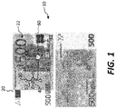
- a hybrid document for example a currency banknote 10, includes a banknote 20 having visible markings 22.
- the banknote 20 can be a government-issued banknote 20 indicated by the visible markings 22 and can comprise a flexible substrate that includes paper, plastic, or impregnated paper.
- One or more light-controlling elements 30 are embedded in or on the banknote 20 and can be printed on the flexible substrate.
- a controller 40 is embedded in or on the banknote 20 and electrically connected to the one or more light-controlling elements 30 for controlling the one or more light-controlling elements 30.
- a power input connection 50 is electrically connected to the controller 40, one or more light-controlling elements 30, or both.
- a power source 60 is electrically connected to the power input connection 50, for example directly to the power input connection 50 (not shown) or through a power convertor 64 (as shown).
- the power source 60 and the controller 40 can be a common element or a common circuit and the controller 40 can be a power conditioning circuit or can include analog or digital control circuitry.
- the controller 40, the light-controlling elements 30 and the power input connection 50 can be electrically connected, for example with wires 52.
- Multiple controllers 40 can be used to provide redundancy, reduce failures, and increase lifetime.
- the multiple controllers 40 can be connected in parallel with common input, output, power, and ground connections.
- the controller 40 can include multiple circuits in multiple integrated circuits and include discrete components, such as capacitors and resistors that can provide additional control support, for example as timing or trimming devices to support light-controlling element 30 flash rates, filter devices such as acoustic wave devices (either bulk or surface).
- discrete components such as capacitors and resistors that can provide additional control support, for example as timing or trimming devices to support light-controlling element 30 flash rates, filter devices such as acoustic wave devices (either bulk or surface).
- the hybrid document can be any document for which authentication is a useful feature, for example government-issued documents such as currency banknotes 20, passports, driver licenses, or identification documents.
- the hybrid document can also be a financial instrument (e.g., banknotes, bonds, bearer bonds, or stock certificates) issued by a financial organization, including central banks, private banks, investment banks, or commercial entities such as corporations.
- the power source 60 can be a piezoelectric power source or a photovoltaic power source and the power convertor 64 can convert the power provided by the power source 60 to a form that is used by the controller 40, the light-controlling elements 30, or both.
- the power convertor 64 can include power storage, for example using capacitors such as thin-film capacitors with a high-K dielectric to provide power over a time period. The capacitors can be distributed, for example located among the power components 62. Output diodes can be used to isolate the power supplies 60 or light-controlling elements 30.
- the power source 60 is indicated by the visible markings 22, the power source 60 forms a part of the visible markings 22, or the power source 60 is obscured by the visible markings 22. Multiple power sources 60 and multiple power convertors 64 can be used to provide redundancy.
- the power source 60 comprises a plurality of electrically connected but physically separated individual power components 62.
- the power components 62 can be arranged in a 2-d array (as shown) or a 1-d array (not shown) and operated by squeezing, waving, or sliding an object across the power components 62.
- the power components 62 can be a group of elements that are operated at the same time with a single action, for example pressure applied to all of the power components 62 simultaneously.
- the power components 62 can be electrically arranged in series to achieve a desired voltage or in parallel to achieve a desired current or some combination of series and parallel to achieve the desired power characteristics.
- the light-controlling elements light-controlling elements 30 can be inorganic light-emitting diodes 30 such as micro-light-emitting diodes suitable for micro-transfer printing, for example made on a semiconductor wafer adapted to the manufacture of inorganic light-emitting diodes 30.
- the light-controlling elements 30 can be light-emitting elements, light-reflecting elements, inorganic light-emitting diodes, organic light-emitting diodes, micro-electromechanical reflective elements, reflective electrophoretic elements, or reflective electrochromic display elements.
- the light-controlling elements 30 of the present invention are referred to below as inorganic light-emitting diodes (iLEDs) 30.
- the present invention contemplates the use of a corresponding variety of light-controlling elements 30.
- the light-controlling elements 30 are also energy harvesting elements (for example silicon photodiodes) and provide power as part of the power source 60.
- the controller 40 can also be an integrated circuit, for example a small chiplet, suitable for micro-transfer printing.
- the controller 40 can include digital circuits or logic (for example CMOS circuits) and power circuits (for example for driving an LED).
- the controller 40 can include information storage circuits, a state machine, or a stored program machine to implement the desired functionality of the hybrid currency banknote 10.
- the controller 40 can read or write information such as currency values, process information, respond to input and provide output.
- the power connection 50 can be directly connected to the controller 40 (as shown) or to the iLEDs 30, or both. Alternatively, the power connection 50 can indirectly connect to the controller 40 or the iLEDs 30, or both through the power convertor 64 (not shown).
- the power connection 50 can be an electrical conductor, for example small wires 52, and can include power connection pads that, when electrically connected to a power source, (such as a 3.3-volt, 5-volt, or 12-volt power source), provides power to the controller 40 and iLEDs 30 to enable them to function.
- a power source such as a 3.3-volt, 5-volt, or 12-volt power source
- the power source can be external (not shown) or can be provided by the internal power source 60.
- the power source 60 comprises a plurality of electrically connected smaller individual power components 62.
- a single large power source 60 can be too rigid to readily fold or curve, whereas an arrangement of individual smaller physically separate power components 62 can allow folding between the smaller power components 62, even if the smaller power components 62 themselves are relatively rigid.
- the iLEDs 30 and controller 40 are too small to be readily visible with the unaided human eye.
- the iLEDs 30 and controller 40 can be located in areas of the banknote 20 that include visible markings 22 to further obscure the presence of the iLEDs 30 and controller 40, as well as any wires 52.
- the power source 60 or an arrangement of individual smaller power components 62 can be obscured by the visible markings 22.
- any of the iLEDs 30, controller 40, wires 52, power source 60, power components 62, or power convertor 64 are marked with visible markings 22.
- ink can be printed over the iLEDs 30, controller 40, wires 52, power source 60, power components 62, or power convertor 64 to obscure them or otherwise make them a part of the visible markings 22 on the banknote 20. Since the iLEDs 30, controller 40, wires 52, power source 60, power components 62, or power convertor 64 can each be very small, for example having a size in the micron range, they can be effectively invisible to the unaided human eye.
- the one or more inorganic micro light-emitting diodes 30 or the controller 40 of the hybrid currency banknote 10 can have a width from 2 to 5 ⁇ m, 5 to 10 ⁇ m, 10 to 20 ⁇ m, or 20 to 50 ⁇ m, a length from 2 to 5 ⁇ m, 5 to 10 ⁇ m, 10 to 20 ⁇ m, or 20 to 50 ⁇ m, or a height from 2 to 5 ⁇ m, 4 to 10 ⁇ m, 10 to 20 ⁇ m, or 20 to 50 ⁇ m.
- the iLEDs 30 and controller 40 are directly printed onto a banknote 20, for example before or after the banknote 20 is printed with ink.
- wires 52 can be woven into the banknote 20 in predetermined locations at which the iLEDs 30 and controller 40 are printed before or after the iLEDs 30 and controller 40 are printed.
- the banknote 20 includes a metalized or metallic ribbon 70 or thread, for example Mylar, with a pattern of electrical conductors or wires 52.
- the iLEDs 30 and controller 40 are printed, for example micro-transfer printed, onto the ribbon 70 before or after the electrical conductors such as wires 52 are formed, patterned, or impressed into the ribbon 70 to make an electrical circuit.
- the iLEDs 30 and controller 40 can include at least a portion of a tether, resulting from the fracturing of a tether on a source wafer from which the iLEDs 30 and controller 40 originate and that connects the iLEDs 30 and controller 40 to an anchor on the source wafer in the micro-transfer printing process.
- the ribbon 70 or thread is then incorporated into the banknote 20 to make an embodiment of the hybrid currency banknote 10 of the present invention.
- the power source 60 (and any power components 62), power convertor 64, or power input connection 50 can likewise be formed in the ribbon 70. Alternatively, some components can be on the ribbon 70 and others not on the ribbon 70, in particular the power source 60.
- the one or more inorganic LEDs 30 are disposed in a location corresponding to a portion of the visible markings 22 to highlight or otherwise indicate the portion of the visible markings 22.
- the one or more inorganic LEDs 30 can underline or surround a graphic element of the visible markings 22.
- the one or more inorganic LEDs 30 outline the numeral 5.
- the one or more inorganic LEDs 30 can be disposed to form a graphic indicator such as any of one or more of a number, a letter, and a pictogram.
- the graphic indicator can have semantic content, for example indicating a value, a date, or a person.
- one or more light pipes 32 are located in association with the one or more inorganic light-emitting diodes 30 to transmit light emitted by the inorganic light-emitting diodes 30 through the light pipes 32 and emit the transmitted light from the opposite end of the light pipe 32.
- the light pipes 32 include portions that leak light at desired locations, for example by purposefully forming nicks, scratches, or other forms of light diffusers 34 in the light pipes 32 to allow light to leak from the light pipe 32.
- the arrangement of the light pipes 32 can also correspond to a portion of the visible markings 22 to highlight or otherwise indicate the portion of the visible markings 22, form a graphic indicator, or form any one or all of a number, a letter, and a pictogram to indicate a value, a date, or a person.
- the controller 40 can control the one or more inorganic light-emitting diodes 30 to flash or sequentially flash individual iLEDs 30, forming spatial, temporal, or temporal-spatial light patterns.
- the inorganic light-emitting diodes 30 can emit different colors of light.
- a red light-emitting diode 82 can emit red light
- a green light-emitting diode 84 can emit green light
- a blue light-emitting diode 86 can emit blue light.
- the different inorganic light-emitting diodes 30 can be arranged spatially to form a display 80, a two-dimensional array, or a graphic element.
- the hybrid currency banknote 10 includes visible markings 22 that do not include a value.
- a hybrid currency banknote 10 can be a non-denominational banknote that either has an assigned value or a variable value stored in a memory 44 in the controller 40, as shown in Fig. 7 .
- an assigned value can be provided by providing a circuit 42 and memory 44 in the controller 40 or providing circuits 42, such as the memory 44, connected to the controller 40.
- the memory 44 can be a read-only memory that encodes a desired assigned value.
- the assigned value can be a currency value or can include an electronic serial number, or both. The assigned value can be discovered by providing power to the power input connection 50.
- the power energizes the controller 40 which, in turn, controls the iLEDs 30 to display or otherwise indicate the assigned value.
- the memory 44 can be protected from overwriting, damage, or alternative discovery by protective layers such as a protective shield 46 formed over the memory 44 to discourage exposure by light and protect the memory 44 from heat.
- the shield 46 can be a light shield, a light reflector, a light absorber, or a heat conductor.
- the memory 44 can be a write-once memory that stores multiple values in memory locations that are ordered in a sequential order, for example by memory address.
- the write-once memory can, for example, employ fuses that are electrically destroyed and cannot be rewritten.
- the memory 44 can be a non-volatile read-write memory.
- the value stored by the hybrid currency banknote 10 can change over time.
- the current value can be discovered by providing power to the power input connection 50. The power energizes the controller 40 which, in turn, controls the iLEDs 30 to display or otherwise indicate the current value.
- the current value can be modified by, for example, a teller machine. Referring to Figs.
- the hybrid currency banknote 10 is adapted to a hybrid currency teller machine 90 that writes a value into the memory 44 in a memory storage location having an address sequentially after the address of a previous written value.
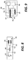
- the power input connection 50 includes or is connected to power connection pads 66 that can be contacted by an external power source to provide power to the controller 40 and iLEDs 30 through wires 52.
- a hybrid currency teller machine 90 includes a slot 91 into which a hybrid currency banknote 10 can be inserted.
- the hybrid currency banknote 10 is read by a reader 92 that can access the controller 40 or memory 44, for example by contacting electrical conductors to the power connection pads. (Only two power connection pads 66 are illustrated, but one or more power connection pads 66 can be included in various embodiments of the present invention).
- a reader 92 that can access the controller 40 or memory 44, for example by contacting electrical conductors to the power connection pads.
- the current value of the hybrid currency banknote 10 can be displayed, for example on an optional teller machine display 96. If a change in the current value of the hybrid currency banknote 10 is desired, an input value can be input by a user with an input device 94.
- a teller machine controller 98 can then calculate or otherwise determine a new stored value responsive to the input value and store the new value in the hybrid currency banknote 10, for example by communicating the new stored value to the controller 40 which then writes the new stored value in the memory 44 with a writer 93.
- the controller 40 only writes new stored values in the memory 44 that are smaller than the current value.
- the controller 40 can write new stored values in the memory 44 that are larger than the current value, or that are larger than the current value but are limited to a maximum value.
- the change in current value of the hybrid currency banknote 10 can represent or be the result of a financial transaction, for example a purchase or a financial exchange with or facilitated by a financial institution such as a bank.
- Read-only memories, write-once memories, and read/write memories together with controllers and read/write circuitry can be formed in integrated circuits and electrical circuits.
- Devices for currency handling, optical inspection, making physical electronic contacts, displays, input devices (such as keyboards or touch screens) can be made using electromechanical, electronic, and optical technologies.
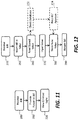
- a hybrid currency banknote 10 of the present invention can be made by providing a banknote 20 with markings in step 100, for example by printing on a high-quality paper with ink using intaglio printing.
- a ribbon 70 is provided in step 110, an inorganic LED wafer having micro-transfer printable iLEDs 30 is provided in step 120, and a controller wafer having micro-transfer printable controllers 40 is provided in step 130.
- the iLEDs 30 are micro-transfer printed from the inorganic LED wafer onto the ribbon 70 using a stamp to fracture tethers connecting the iLEDs 30 to the inorganic LED wafer leaving at least a portion of a tether on the iLEDs 30 in step 140.
- the controllers 40 are micro-transfer printed from the controller wafer onto the ribbon 70 using a stamp to fracture tethers connecting the controllers 40 to the controller wafer leaving at least a portion of a tether on the controllers 40 in step 150.
- the power source 60 is similarly micro-transfer printed to the ribbon 70 in step 160.
- Power connection pads 66, wires 52 and any other necessary electrical conductors are formed in step 170 to make an electronic circuit having electrical conductors.
- the electrical conductors can be provided before or after the iLEDs 30 and controllers 40 are micro-transfer printed.
- the ribbon 70 can be further processed, for example to provide environmental robustness by coating with protective layers.
- the ribbon 70 is then integrated into the banknote 20 in step 180 to make the hybrid currency banknote 10 of the present invention.
- the hybrid currency banknote 10 can be further processed, for example by over coating or printing to provide environmental robustness, decoration, or to obscure the micro-transfer printed elements.
- the hybrid currency banknote 10 of the present invention can be used by first receiving the hybrid currency banknote 10 in step 200, providing power to the hybrid currency banknote 10 in step 210, and viewing light emitted by the hybrid currency banknote 10 in step 220.
- Power can be provided by connecting the hybrid currency banknote 10 to an external power source (e.g., using the power connection pads 66), squeezing a piezoelectric power source 60, or exposing a photovoltaic power source 60 to light.
- an assigned or current value can be programmed into the controller 40 or an associated memory 44 (also micro-transfer printed if it is a separate integrated circuit or chiplet) either before or after the controller 40 or memory 44 is micro-transfer printed.
- an external device such as a hybrid currency teller machine 90 can communicate with the controller to write an assigned or current value to the hybrid currency banknote 10.
- the hybrid currency banknote 10 can be received in step 200, inserted into the hybrid currency teller machine 90 in step 250, the current value read by the reader 92 in step 260, an input value input by the input device 94 in step 270, a new stored value responsive to the input value computed by the teller machine controller 98 and stored by the writer 93 in step 280 and the hybrid currency banknote 10 returned in step 290.
- the hybrid currency teller machine 90 can also communicate with a central or remote database (step 272) to establish the legitimacy of the hybrid currency banknote 10, track its use or location, or approve a transaction and record or approve the transaction (step 274).
- the communication can include an electronic serial number.
- U.S. Patent Application Serial No. 14/743,981 filed June 18, 2015 , entitled Micro Assembled LED Displays and Lighting Elements, describes micro-transfer printing structures and processes useful with the present invention.
- micro-transfer printing techniques see also U.S. Patent Nos. 8,722,458 , 7,622,367 and 8,506,867 .
- Micro-transfer printing using compound micro assembly structures and methods can also be used with the present invention, for example, as described in U.S. Patent Application Serial No. 14/822,868, filed August 10, 2015 , entitled Compound Micro-Assembly Strategies and Devices .
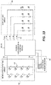
- a power source 60 includes two parallel groups of four series-connected power components 62 electrically connected to the power connection 50 and the power convertor 64 and controller 40.
- the power convertor 64 and controller 40 can be a single component, as shown, or include multiple different components such as separate integrated circuits.
- Control current from the power convertor 64 and controller 40 drives the iLEDs 30 of the display 80.
- a capacitive touch sensor 68 is also included ( Fig. 13 ).
- the power source 60 is a photovoltaic power source.
- the power source 60 is a piezoelectric power source. Fig.
- FIG. 15 illustrates an example power convertor 64 and controller 40 having a four-diode bridge rectifier and storage capacitor C R providing power from a piezoelectric power source 60 to a current limiter that, in turn, provides current to the iLEDs 30.
- the controller 40 can be powered by the power component 60 to control the iLEDs 30, but is not illustrated in Fig. 15 .
- the controller 40 and power component 60 can be a common component or circuit or can be separate or individual components or circuits.
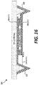
- a power component 64 can include a dielectric layer such as a silicon nitride layer with a first metal layer providing a first connection post 69 or spike.
- a piezoelectric material layer is in electrical contact with the first metal layer and, on a side of the piezoelectric material layer opposite the first metal layer, a second metal layer is in electrical contact with a second metal layer and forms a second connection post 69 or spike.
- the power component 64 of Fig. 16 can be micro-transfer printed onto two conductors (e.g., wires 52) so that the first and second connection posts 69 are in contact with the conductors.
- the first and second connection posts 69 can pierce or otherwise deform and adhere to the conductors after micro-transfer printing.
- Fig. 17 illustrates the process of making a banknote 20 according to an embodiment of the present invention.
- a printed banknote is provided together with a ribbon 70 having an array of micro-transfer printed iLEDs 30 electrically connected to a controller, a power convertor 64, and a power source 60.
- the ribbon 70 is laminated or otherwise integrated into the banknote 20 to make a hybrid currency banknote 10.
- a hybrid currency banknote 10 of the present invention having a photovoltaic power source 60 can be exposed to ambient illumination to provide power to iLEDs 30 in a display 80, causing the iLEDs 30 to emit light. It has been calculated that conventional ambient office light provides sufficient illumination (e.g., 500 lux) to operate a photovoltaic embodiment of the present invention, including digital control for iLEDs 30 sequencing, for example flashing.
- Photovoltaic cells e.g., power components 62
- the array of power components 62 can occupy a larger area with a lower fill factor to provide apparent transparency and improved flexibility to the power source 60.
- a 20 x 20 array of 400 iLEDs 30 (for example, green-light-emitting iLEDs 30) can provide a readable display 80 in these conditions over a viewing angle of 140 degrees similar to displays found in body-worn electronic devices (e.g., watches, fitness trackers) and can consume 66 ⁇ W.
- a hybrid currency banknote 10 of the present invention having a piezoelectric power source 60 can be pressed or squeezed, for example, by a finger, to provide power to iLEDs 30 in a display 80, causing the iLEDs 30 to emit light. Power is provided both when pressing and releasing (hence the use of a bridge rectifier in Fig. 15 ). It has been demonstrated that a fingertip having a one square cm area can provide a force of 35 N. Even with a smaller force of 10 N, a piezoelectric power source 60 with a total area of 0.06 cm 2 provides sufficient power to operate a piezoelectric embodiment of the present invention, including digital control for iLEDs 30 sequencing, for example flashing.
- the array of power components 62 can occupy a larger area (e.g., 0.5 cm 2 with a lower fill factor to provide apparent transparency and improved flexibility to the power source 60.
- a hybrid currency banknote 10 can have one or more energy output devices embedded in or on the banknote.
- the one or more energy output devices can be one or more of one or more light-emitting elements, a sound-emitting element, and a vibration element.
- the sound-emitting element can be a piezoelectric speaker and the vibration device can be a piezoelectric device.
- the elements can be controlled, powered, hidden, constructed, or otherwise provided in ways similar to those of the light-emitting elements 30 discussed at greater length above. Such alternative energy output modalities can be useful for persons with impaired vision.
- a first layer on a second layer in some embodiments means a first layer directly on and in contact with a second layer. In other embodiments, a first layer on a second layer can include another layer there between.
Landscapes
- Physics & Mathematics (AREA)
- General Physics & Mathematics (AREA)
- Engineering & Computer Science (AREA)
- Manufacturing & Machinery (AREA)
- Toxicology (AREA)
- Health & Medical Sciences (AREA)
- General Health & Medical Sciences (AREA)
- Accounting & Taxation (AREA)
- Finance (AREA)
- Business, Economics & Management (AREA)
- Credit Cards Or The Like (AREA)
- Inspection Of Paper Currency And Valuable Securities (AREA)
- Illuminated Signs And Luminous Advertising (AREA)
Description
- This application claims priority to and benefit of
U.S. Patent Application No. 15/433,119, filed February 15, 2017 U.S. Patent Application No. 62/301,211, filed February 29, 2016 - The present invention relates to currency and particularly to banknotes having electronically controlled inorganic light-emitting diodes embedded in the banknotes.
- Monetary instruments issued by governments such as money or currency are used throughout the world today. Government-issued currency typically includes banknotes (also known as paper currency or bills) having visible markings printed on high-quality paper, plastic, or paper impregnated with other materials, such as plastic. The visible markings indicate the denomination (value) of the banknote, includes a serial number, and has decorations such as images, and anti-counterfeiting structures such as special threads, ribbons, and holograms. Currency circulates within an economic system as a medium of monetary exchange having a fixed value until it is physically worn out. Worn out banknotes are generally returned by banks or other financial institutions and then replaced.
- Other privately issued monetary instruments are also used, such as credit cards and gift cards. These cards typically include an electronically accessible value (e.g., stored in a magnetic stripe or in a chip in the card) or an electronically accessible account that can be used to make purchases. However, the value of the card is not readily viewed by a user without special equipment, such as a reader.
- In the past, banknotes have not been electronically enabled. However, more recently there have been proposals to use RFID (radio-frequency identification device) in banknotes to validate the banknote and avoid counterfeiting. For example,
U.S. Patent No. 8,391,688 andU.S. Patent No. 8,791,822 disclose systems for currency validation.U.S. Patent No. 5,394,969 describes a capacitance-based verification device for a security thread embedded within currency paper to defeat counterfeiting. Security systems for scanning a paper banknote and checking identification information in the banknote (e.g., the serial number) with a network-accessible database have been proposed, for example inU.S. Patent No. 6,131,718 . In all of these systems, however, there is no way to visibly test small details of a banknote without using a separate electronic or optical reader. - There remains a need therefore, for currency providing a variable value that is electronically accessible with visible indicia without using a separate electronic or optical reader.
- Patent document
US 2005/150740 A1 discloses a banknote having an electronic circuit that communicates with an optical security device using optical communication. J - The present invention provides a hybrid document, for example a currency banknote, having visible markings and one or more light-controlling elements, for example inorganic light-emitting diodes (iLEDs), and a controller embedded in or on the banknote and electrically connected to control the light-controlling elements to emit light. A power input connection is electrically connected to the controller, or one or more light-controlling elements, or both. In a further embodiment, a power source, such as a piezoelectric or photovoltaic device, is electrically connected to the power input connection, with or without a power convertor. In various embodiments, the visible markings include printed images or value indicators. The light-controlling elements can form a graphic indicator such as a number, letter, or pictogram or can highlight a visible marking on the banknote. The light-controlling elements can form a display, for example a monochrome or full-color display.
- In one embodiment, the light-controlling elements or controller are printed on the pre-printed banknote. In another embodiment, the light-controlling elements or controller is printed on a ribbon or thread that is subsequently woven or otherwise incorporated into the banknote. The ribbon or thread can also include electrical conductors to electrically connect the controller, the light-controlling elements, and the power source in a circuit. When operated by applying power, the controller controls the light-controlling elements to emit light, for example in a spatial pattern, or in a temporal pattern (for example with flashing lights or sequentially flashing lights), or both. Different light-controlling
elements 30 can be activated in response to sequential squeezes of thepiezoelectric power source 60. - The currency can also include light pipes (optical waveguides) arranged in association with the light-controlling elements. The light pipes can conduct light to desired locations on the banknote or can form patterns such as graphic indicators. The light pipes can include light-emitting portions, for example diffusers, along the length of the light pipes to emit light at locations along the length of the light pipe as well as at the end of the light pipe.
- The controller can include a memory, for example a read-only memory or a write-once memory storing one or more values and the light-controlling elements can be controlled to display numerals corresponding to the values. Multiple values can be stored in a sequential order corresponding to a temporally sequential set of values and can monotonically decline in magnitude. Values stored in the banknote can be electronically read by a teller machine having a reader and the value of the banknote displayed on the teller machine. In a further embodiment, the teller machine can write a value to the banknote using a writer. In an embodiment, the controller controls the written value so that it must be equal to or smaller than a value already stored in the banknote.
- A method of making a hybrid currency banknote includes providing a banknote having visible markings, a wafer having a plurality of micro-transfer printable light-controlling elements, and a wafer having a plurality of controllers. One or more of the light-controlling elements and at least one controller are embedded in the banknote, for example by micro-transfer printing onto the banknote or onto a thread or ribbon that is subsequently incorporated into the banknote. The controller is electrically connected to the one or more light-controlling elements and to a power input connection. A power source can also be provided, for example by micro-transfer printing the power source on the banknote or ribbon. An issuer of the hybrid currency banknote can provide a memory with a value or write the value to a memory in the banknote to provide the banknote with a value.
- The hybrid currency banknote of the present invention can be used by receiving the banknote and providing power to the power input connection, for example by a teller machine that then displays the value of the banknote on the banknote itself or on a display incorporated into the teller machine. Alternatively, the banknote includes a piezoelectric power source and upon squeezing the power source the controller controls the light-controlling elements to emit light. In another embodiment, the banknote includes a photovoltaic power source and upon exposure to electromagnetic radiation (such as infrared or ultraviolet radiation), the controller controls the light-controlling elements to emit light.
- A user can insert a received banknote into a teller machine, input an input value to the teller machine, and the teller machine can write a value derived from the input value into the banknote. The input value can represent the value of a monetary transaction, for example a purchase of goods or payment of debt and the difference between the input value and the current value can be written into the hybrid currency banknote.
- The present invention provides an anonymous, government-issued currency with anti-counterfeiting light emitters whose value can be visibly ascertained without requiring specialized equipment and modified electronically.
- In one aspect, the disclosed technology includes a hybrid currency banknote, including: a banknote having visible markings; one or more light-emitting elements embedded in or on the banknote; a controller embedded in or on the banknote electrically connected to the one or more light-controlling elements for controlling the one or more light-controlling elements; and a power input connection electrically connected to the controller, or one or more light-emitting elements, or both.
- In certain embodiments, the light-controlling elements are light-emitting elements, light-reflecting elements, inorganic light-emitting diodes, organic light-emitting diodes, micro-electromechanical reflective elements, reflective electrophoretic elements, or reflective electrochromic display elements.
- In certain embodiments, the banknote includes a power source connected to the power input connection.
- In certain embodiments, the power source is a piezoelectric power source or a photovoltaic power source.
- In certain embodiments, the power source is indicated by the visible markings, the power source forms a part of the visible markings, or the power source is obscured by the visible markings.
- In certain embodiments, the power source comprises a plurality of electrically connected individual power source components.
- In certain embodiments, the banknote includes a power convertor connected to the power input connection and the controller or one or more light-controlling elements.
- In certain embodiments, the banknote is a government-issued banknote indicated by the visible markings.
- In certain embodiments, the banknote includes a flexible substrate that includes paper, plastic, or impregnated paper, and the one or more light-controlling elements and the controller are printed on the flexible substrate.
- In certain embodiments, the banknote includes a ribbon or thread woven into the banknote and the and the one or more light-controlling elements and the controller are printed on the ribbon or thread.
- In certain embodiments, the ribbon or thread or portions of the ribbon or thread are at least partially electrically conductive or include conductive wires.
- In certain embodiments, the one or more light-controlling elements, the controller, or both the one or more light-controlling elements and the controller include at least a portion of a tether.
- In certain embodiments, the one or more light-controlling elements are disposed in a location corresponding to a portion of the visible markings to highlight or otherwise indicate the portion of the visible markings.
- In certain embodiments, the one or more light-controlling elements are disposed to form a graphic indicator.
- In certain embodiments, the graphic indicator is any of one or more of a number, a letter, and a pictogram.
- In certain embodiments, the graphic indicator indicates a value, a date, or a person.
- In certain embodiments, the banknote includes one or more light pipes located in association with the one or more light-controlling elements.
- In certain embodiments, the light pipes include portions that leak light at desired locations.
- In certain embodiments, the one or more light pipes are disposed in a location or arranged in a pattern corresponding to a portion of the visible markings to highlight or otherwise indicate the portion of the visible markings.
- In certain embodiments, the one or more light pipes are disposed to form a graphic indicator.
- In certain embodiments, the graphic indicator is any of one or more of a number, a letter, and a pictogram.
- In certain embodiments, the graphic indicator indicates a value, a date, or a person.
- In certain embodiments, the controller controls the one or more light-controlling elements to flash or flash sequentially.
- In certain embodiments, the one or more light-controlling elements include inorganic light-emitting diodes that emit different colors of light.
- In certain embodiments, the different colors of light include red, green, and blue.
- In certain embodiments, the one or more light-controlling elements forms a display or a two-dimensional array.
- In certain embodiments, the visible markings do not include a value.
- In certain embodiments, the one or more light-controlling elements are arranged to indicate a value.
- In certain embodiments, the controller includes protective layers disposed over at least one or more portions of the controller.
- In certain embodiments, the controller includes a circuit having a memory that stores a value and the circuit causes the one or more light-controlling elements to indicate the value or the memory stores an electronic serial number.
- In certain embodiments, the memory is a read-only memory.
- In certain embodiments, the memory is a write-once memory that stores multiple values in memory locations that are ordered in a sequential order.
- In certain embodiments, the banknote is adapted to a teller machine that writes a value into the memory in a location sequentially after the previous written value.
- In certain embodiments, the one or more light-controlling elements or the controller has a width from 2 to 5 µm, 5 to 10 µm, 10 to 20 µm, or 20 to 50 µm, a length from 2 to 5 µm, 5 to 10 µm, 10 to 20 µm, or 20 to 50 µm, or a height from 2 to 5 µm, 4 to 10 µm, 10 to 20 µm, or 20 to 50 µm.
- In another aspect, the disclosed technology includes a hybrid currency teller machine, including an optional display and a reader adapted to accept the hybrid currency banknote (e.g., as described above), read one or more of the values stored in the memory, and optionally display the read value on the display.
- In certain embodiments, the hybrid currency teller machine includes an input device for accepting an input value and a writer for writing a new stored value responsive to the input value in the memory.
- In certain embodiments, the disclosed technology includes a method of making a hybrid currency banknote, the method including: providing a banknote having visible markings; providing a wafer having a plurality of micro-transfer printable light-controlling elements; providing a wafer having a plurality of controllers; embedding one or more of the light-controlling elements and at least one controller to the banknote; and electrically connecting the controller to the one or more light-controlling elements and to a power input connection.
- In certain embodiments, the method includes micro-transfer printing the light-controlling elements and at least one controller to the banknote.
- In certain embodiments, the method includes providing ribbon or thread, micro-transfer printing the light-controlling elements and at least one controller to the ribbon or thread, and integrating the micro-transfer printed ribbon or thread in the banknote.
- In certain embodiments, the method includes providing a power source on the banknote and electrically connecting the power source to the power input connection.
- In certain embodiments, the controller includes a memory and comprising providing the memory with a value.
- In another aspect, the disclosed technology includes a method of using a hybrid currency banknote according to
claim 1, the method including: receiving the banknote; providing power to the power input connection; and viewing light emitted by the one or more light-controlling elements. - In certain embodiments, the method includes inserting the hybrid currency banknote into a teller machine (e.g., as described above).
- In certain embodiments, the method includes communicating an identification of the hybrid currency banknote to a remote database and receiving a communication from the database.
- In certain embodiments, the communicated identity is recorded by the remote database.
- In certain embodiments, the method includes inserting the hybrid currency banknote into a hybrid currency teller machine according to claim 35, entering an input value with the input device, and retrieving the hybrid currency banknote from the hybrid currency teller machine, the hybrid currency banknote having a new stored value responsive to the input value.
- In certain embodiments, the new stored value is the difference between a previously stored value and the input value.
- In certain embodiments, the method includes communicating an identification of the hybrid currency banknote to a remote database and receiving a communication from the remote database.
- In certain embodiments, the received communication is an approval or disapproval and the hybrid currency banknote has a new stored value responsive to the input value only if an approval is received.
- In certain embodiments, the input value represents a desired transaction and the remote database records the transaction.
- In certain embodiments, the hybrid currency banknote comprises a power source connected to the power input connection.
- In certain embodiments, the power source is a piezoelectric power source and comprising squeezing the piezoelectric power source.
- In certain embodiments, the power source is a photovoltaic power source and comprising exposing the photovoltaic power source to photons.
- In another aspect, the disclosed technology includes a hybrid currency banknote, including: a banknote having visible markings; one or more energy output devices embedded in or on the banknote; a controller embedded in or on the banknote electrically connected to the one or more energy output devices for controlling the one or more energy output devices; and a power input connection electrically connected to the controller, or to the one or energy output devices, or both.
- In certain embodiments, the one or energy output devices is one or more of one or more light-emitting elements, a sound-emitting element, and a vibration element.
- In another aspect, the disclosed technology includes a hybrid document, including: a document having visible markings; one or more light-emitting elements embedded in or on the document; a controller embedded in or on the banknote electrically connected to the one or more light-controlling elements for controlling the one or more light-controlling elements; and a power input connection electrically connected to the controller, or one or more light-emitting elements, or both.
- In certain embodiments, the light-controlling elements are light-emitting elements, light-reflecting elements, inorganic light-emitting diodes, organic light-emitting diodes, micro-electromechanical reflective elements, reflective electrophoretic elements, or reflective electrochromic display elements.
- In certain embodiments, the hybrid document includes a power source connected to the power input connection.
- In certain embodiments, the power source is a piezoelectric power source or a photovoltaic power source.
- In certain embodiments, the power source is indicated by the visible markings, the power source forms a part of the visible markings, or the power source is obscured by the visible markings.
- In certain embodiments, the power source comprises a plurality of electrically connected individual power source components.
- In certain embodiments, the hybrid banknote includes a power convertor connected to the power input connection and the controller or one or more light-controlling elements.
- In certain embodiments, the banknote is a government-issued banknote indicated by the visible markings.
- In certain embodiments, the banknote includes a flexible substrate that includes paper, plastic, or impregnated paper, and the one or more light-controlling elements and the controller are printed on the flexible substrate.
- In certain embodiments, the banknote includes a ribbon or thread woven into the banknote and the and the one or more light-controlling elements and the controller are printed on the ribbon or thread.
- In certain embodiments, the ribbon or thread or portions of the ribbon or thread are at least partially electrically conductive or include conductive wires.
- In certain embodiments, the one or more light-controlling elements, the controller, or both the one or more light-controlling elements and the controller include at least a portion of a tether.
- In certain embodiments, the one or more light-controlling elements are disposed in a location corresponding to a portion of the visible markings to highlight or otherwise indicate the portion of the visible markings.
- In certain embodiments, the one or more light-controlling elements are disposed to form a graphic indicator.
- In certain embodiments, the graphic indicator is any of one or more of a number, a letter, and a pictogram.
- In certain embodiments, the graphic indicator indicates a value, a date, or a person.
- In certain embodiments, the hybrid banknote includes one or more light pipes located in association with the one or more light-controlling elements.
- In certain embodiments, the light pipes include portions that leak light at desired locations.
- In certain embodiments, the one or more light pipes are disposed in a location or arranged in a pattern corresponding to a portion of the visible markings to highlight or otherwise indicate the portion of the visible markings.
- In certain embodiments, the one or more light pipes are disposed to form a graphic indicator.
- In certain embodiments, the graphic indicator is any of one or more of a number, a letter, and a pictogram.
- In certain embodiments, the graphic indicator indicates a value, a date, or a person.
- In certain embodiments, the controller controls the one or more light-controlling elements to flash or flash sequentially.
- In certain embodiments, the one or more light-controlling elements include inorganic light-emitting diodes that emit different colors of light.
- In certain embodiments, the different colors of light include red, green, and blue.
- In certain embodiments, the one or more light-controlling elements forms a display or a two-dimensional array.
- In certain embodiments, the visible markings do not include a value.
- In certain embodiments, the one or more light-controlling elements are arranged to indicate a value.
- In certain embodiments, the controller includes protective layers disposed over at least one or more portions of the controller.
- In certain embodiments, the controller includes a circuit having a memory that stores a value and the circuit causes the one or more light-controlling elements to indicate the value or the memory stores an electronic serial number.
- In certain embodiments, the memory is a read-only memory.
- In certain embodiments, the memory is a write-once memory that stores multiple values in memory locations that are ordered in a sequential order.
- In certain embodiments, the banknote is adapted to a teller machine that writes a value into the memory in a location sequentially after the previous written value.
- In certain embodiments, the one or more light-controlling elements or the controller has a width from 2 to 5 µm, 5 to 10 µm, 10 to 20 µm, or 20 to 50 µm , a length from 2 to 5 µm, 5 to 10 µm, 10 to 20 µm, or 20 to 50 µm, or a height from 2 to 5 µm, 4 to 10 µm, 10 to 20 µm, or 20 to 50 µm.
- In another aspect, the disclosed technology includes a method of making a hybrid document, including: providing a banknote having visible markings; providing a wafer having a plurality of micro-transfer printable light-controlling elements; providing a wafer having a plurality of controllers; embedding one or more of the light-controlling elements and at least one controller to the document; and electrically connecting the controller to the one or more light-controlling elements and to a power input connection.
- In certain embodiments, the method includes micro-transfer printing the light-controlling elements and at least one controller to the document.
- In certain embodiments, the method includes providing ribbon or thread, micro-transfer printing the light-controlling elements and at least one controller to the ribbon or thread, and integrating the micro-transfer printed ribbon or thread in the document.
- In certain embodiments, the method includes providing a power source on the document and electrically connecting the power source to the power input connection.
- In certain embodiments, the controller includes a memory and comprising providing the memory with a value.
- In another aspect, the disclosed technology includes a method of using a hybrid document (e.g., as described above), including: receiving the document; providing power to the power input connection; and viewing light emitted by the one or more light-controlling elements.
- In certain embodiments, the method includes communicating an identification of the hybrid document to a remote database and receiving a communication from the database.
- In certain embodiments, the communicated identity is recorded by the remote database.
- In another aspect, the disclosed technology includes a hybrid document, including: a banknote having visible markings; one or more energy output devices embedded in or on the banknote; a controller embedded in or on the banknote electrically connected to the one or more energy output devices for controlling the one or more energy output devices; and a power input connection electrically connected to the controller, or to the one or energy output devices, or both.
- In certain embodiments, the one or energy output devices is one or more of one or more light-emitting elements, a sound-emitting element, and a vibration element.
- The foregoing and other objects, aspects, features, and advantages of the present disclosure will become more apparent and better understood by referring to the following description taken in conjunction with the accompanying drawings, in which:
-
Fig. 1 is a plan view of the front and back sides of an embodiment of the present invention; -
Fig. 2 is a schematic diagram according to an embodiment of the present invention; -
Fig. 3 is a plan view of the front and back sides of another embodiment of the present invention; -
Fig. 4 is an illustration of a light pipe according to an embodiment of the present invention; -
Fig. 5 is a schematic illustration of a display according to an embodiment of the present invention; -
Fig. 6 is a schematic diagram of one side of a hybrid currency banknote according to another embodiment of the present invention; -
Fig. 7 is a schematic diagram illustrating a controller and circuit according to another embodiment of the present invention; -
Fig. 8 is a schematic diagram illustrating a circuit according to another embodiment of the present invention; -
Fig. 9 is a schematic of a teller machine according to an embodiment of the present invention; -
Figs. 10-12 are flow charts illustrating methods of the present invention; -
Figs. 13-15 are schematic diagrams according to embodiments of the present invention; -
Fig. 16 is a cross section of a piezoelectric power component according to an embodiment of the present invention; -
Fig. 17 is a schematic illustration of a method according to an embodiment of the present invention; and -
Figs. 18 and19 are schematic illustrations of methods of operating an embodiment of the present invention. - The features and advantages of the present disclosure will become more apparent from the detailed description set forth below when taken in conjunction with the drawings, in which like reference characters identify corresponding elements throughout. In the drawings, like reference numbers generally indicate identical, functionally similar, and/or structurally similar elements. The figures are not drawn to scale since the variation in size of various elements in the Figures is too great to permit depiction to scale.
- Referring to
Fig. 1 , in an embodiment of the present invention a hybrid document, for example acurrency banknote 10, includes abanknote 20 havingvisible markings 22. Thebanknote 20 can be a government-issuedbanknote 20 indicated by thevisible markings 22 and can comprise a flexible substrate that includes paper, plastic, or impregnated paper. One or more light-controllingelements 30 are embedded in or on thebanknote 20 and can be printed on the flexible substrate. Acontroller 40 is embedded in or on thebanknote 20 and electrically connected to the one or more light-controllingelements 30 for controlling the one or more light-controllingelements 30. Apower input connection 50 is electrically connected to thecontroller 40, one or more light-controllingelements 30, or both. In a further embodiment, apower source 60 is electrically connected to thepower input connection 50, for example directly to the power input connection 50 (not shown) or through a power convertor 64 (as shown). Thepower source 60 and thecontroller 40 can be a common element or a common circuit and thecontroller 40 can be a power conditioning circuit or can include analog or digital control circuitry. Thecontroller 40, the light-controllingelements 30 and thepower input connection 50 can be electrically connected, for example withwires 52.Multiple controllers 40 can be used to provide redundancy, reduce failures, and increase lifetime. Themultiple controllers 40 can be connected in parallel with common input, output, power, and ground connections. In other embodiments, thecontroller 40 can include multiple circuits in multiple integrated circuits and include discrete components, such as capacitors and resistors that can provide additional control support, for example as timing or trimming devices to support light-controllingelement 30 flash rates, filter devices such as acoustic wave devices (either bulk or surface). - In embodiments of the present invention, the hybrid document can be any document for which authentication is a useful feature, for example government-issued documents such as
currency banknotes 20, passports, driver licenses, or identification documents. The hybrid document can also be a financial instrument (e.g., banknotes, bonds, bearer bonds, or stock certificates) issued by a financial organization, including central banks, private banks, investment banks, or commercial entities such as corporations. - The
power source 60 can be a piezoelectric power source or a photovoltaic power source and thepower convertor 64 can convert the power provided by thepower source 60 to a form that is used by thecontroller 40, the light-controllingelements 30, or both. Thepower convertor 64 can include power storage, for example using capacitors such as thin-film capacitors with a high-K dielectric to provide power over a time period. The capacitors can be distributed, for example located among thepower components 62. Output diodes can be used to isolate the power supplies 60 or light-controllingelements 30. In one arrangement, thepower source 60 is indicated by thevisible markings 22, thepower source 60 forms a part of thevisible markings 22, or thepower source 60 is obscured by thevisible markings 22.Multiple power sources 60 andmultiple power convertors 64 can be used to provide redundancy. - In an embodiment, the
power source 60 comprises a plurality of electrically connected but physically separatedindividual power components 62. Thepower components 62 can be arranged in a 2-d array (as shown) or a 1-d array (not shown) and operated by squeezing, waving, or sliding an object across thepower components 62. Thepower components 62 can be a group of elements that are operated at the same time with a single action, for example pressure applied to all of thepower components 62 simultaneously. Thepower components 62 can be electrically arranged in series to achieve a desired voltage or in parallel to achieve a desired current or some combination of series and parallel to achieve the desired power characteristics. - The light-controlling elements light-controlling
elements 30 can be inorganic light-emittingdiodes 30 such as micro-light-emitting diodes suitable for micro-transfer printing, for example made on a semiconductor wafer adapted to the manufacture of inorganic light-emittingdiodes 30. In general, the light-controllingelements 30 can be light-emitting elements, light-reflecting elements, inorganic light-emitting diodes, organic light-emitting diodes, micro-electromechanical reflective elements, reflective electrophoretic elements, or reflective electrochromic display elements. For clarity of exposition, the light-controllingelements 30 of the present invention are referred to below as inorganic light-emitting diodes (iLEDs) 30. However, in various embodiments the present invention contemplates the use of a corresponding variety of light-controllingelements 30. In another embodiment, the light-controllingelements 30 are also energy harvesting elements (for example silicon photodiodes) and provide power as part of thepower source 60. - The
controller 40 can also be an integrated circuit, for example a small chiplet, suitable for micro-transfer printing. Thecontroller 40 can include digital circuits or logic (for example CMOS circuits) and power circuits (for example for driving an LED). Thecontroller 40 can include information storage circuits, a state machine, or a stored program machine to implement the desired functionality of thehybrid currency banknote 10. Thecontroller 40 can read or write information such as currency values, process information, respond to input and provide output. Thepower connection 50 can be directly connected to the controller 40 (as shown) or to theiLEDs 30, or both. Alternatively, thepower connection 50 can indirectly connect to thecontroller 40 or theiLEDs 30, or both through the power convertor 64 (not shown). Thepower connection 50 can be an electrical conductor, for examplesmall wires 52, and can include power connection pads that, when electrically connected to a power source, (such as a 3.3-volt, 5-volt, or 12-volt power source), provides power to thecontroller 40 andiLEDs 30 to enable them to function. The power source can be external (not shown) or can be provided by theinternal power source 60. - It can be desirable to fold or spindle the
hybrid currency banknote 10 of the present invention. To facilitate such a manipulation, in an embodiment of the present invention, thepower source 60 comprises a plurality of electrically connected smallerindividual power components 62. A singlelarge power source 60 can be too rigid to readily fold or curve, whereas an arrangement of individual smaller physicallyseparate power components 62 can allow folding between thesmaller power components 62, even if thesmaller power components 62 themselves are relatively rigid. - In a further embodiment, the
iLEDs 30 andcontroller 40 are too small to be readily visible with the unaided human eye. Furthermore, theiLEDs 30 andcontroller 40 can be located in areas of thebanknote 20 that includevisible markings 22 to further obscure the presence of theiLEDs 30 andcontroller 40, as well as anywires 52. Similarly, thepower source 60 or an arrangement of individualsmaller power components 62 can be obscured by thevisible markings 22. In one embodiment, any of theiLEDs 30,controller 40,wires 52,power source 60,power components 62, orpower convertor 64 are marked withvisible markings 22. For example, ink can be printed over theiLEDs 30,controller 40,wires 52,power source 60,power components 62, orpower convertor 64 to obscure them or otherwise make them a part of thevisible markings 22 on thebanknote 20. Since theiLEDs 30,controller 40,wires 52,power source 60,power components 62, orpower convertor 64 can each be very small, for example having a size in the micron range, they can be effectively invisible to the unaided human eye. For example, the one or more inorganic micro light-emittingdiodes 30 or thecontroller 40 of thehybrid currency banknote 10 can have a width from 2 to 5 µm, 5 to 10 µm, 10 to 20 µm, or 20 to 50 µm, a length from 2 to 5 µm, 5 to 10 µm, 10 to 20 µm, or 20 to 50 µm, or a height from 2 to 5 µm, 4 to 10 µm, 10 to 20 µm, or 20 to 50 µm. - In one embodiment of the present invention, the
iLEDs 30 andcontroller 40 are directly printed onto abanknote 20, for example before or after thebanknote 20 is printed with ink. In this embodiment,wires 52 can be woven into thebanknote 20 in predetermined locations at which the iLEDs 30 andcontroller 40 are printed before or after the iLEDs 30 andcontroller 40 are printed. Referring toFig. 2 in another embodiment, thebanknote 20 includes a metalized ormetallic ribbon 70 or thread, for example Mylar, with a pattern of electrical conductors orwires 52. The iLEDs 30 andcontroller 40 are printed, for example micro-transfer printed, onto theribbon 70 before or after the electrical conductors such aswires 52 are formed, patterned, or impressed into theribbon 70 to make an electrical circuit. In such an embodiment, theiLEDs 30 andcontroller 40 can include at least a portion of a tether, resulting from the fracturing of a tether on a source wafer from which the iLEDs 30 andcontroller 40 originate and that connects the iLEDs 30 andcontroller 40 to an anchor on the source wafer in the micro-transfer printing process. Theribbon 70 or thread is then incorporated into thebanknote 20 to make an embodiment of thehybrid currency banknote 10 of the present invention. The power source 60 (and any power components 62),power convertor 64, orpower input connection 50 can likewise be formed in theribbon 70. Alternatively, some components can be on theribbon 70 and others not on theribbon 70, in particular thepower source 60. - Referring to
Fig. 3 , in an embodiment the one or moreinorganic LEDs 30 are disposed in a location corresponding to a portion of thevisible markings 22 to highlight or otherwise indicate the portion of thevisible markings 22. For example, the one or moreinorganic LEDs 30 can underline or surround a graphic element of thevisible markings 22. As shown inFig. 3 , the one or moreinorganic LEDs 30 outline the numeral 5. Thus, the one or moreinorganic LEDs 30 can be disposed to form a graphic indicator such as any of one or more of a number, a letter, and a pictogram. The graphic indicator can have semantic content, for example indicating a value, a date, or a person. - Referring next to
Fig. 4 , one or morelight pipes 32 are located in association with the one or more inorganic light-emittingdiodes 30 to transmit light emitted by the inorganic light-emittingdiodes 30 through thelight pipes 32 and emit the transmitted light from the opposite end of thelight pipe 32. In an embodiment, thelight pipes 32 include portions that leak light at desired locations, for example by purposefully forming nicks, scratches, or other forms oflight diffusers 34 in thelight pipes 32 to allow light to leak from thelight pipe 32. Thus, the arrangement of thelight pipes 32 can also correspond to a portion of thevisible markings 22 to highlight or otherwise indicate the portion of thevisible markings 22, form a graphic indicator, or form any one or all of a number, a letter, and a pictogram to indicate a value, a date, or a person. - The
controller 40 can control the one or more inorganic light-emittingdiodes 30 to flash or sequentially flashindividual iLEDs 30, forming spatial, temporal, or temporal-spatial light patterns. Referring toFig. 5 , in an embodiment, the inorganic light-emittingdiodes 30 can emit different colors of light. For example, a red light-emittingdiode 82 can emit red light, a green light-emittingdiode 84 can emit green light, and a blue light-emittingdiode 86 can emit blue light. The different inorganic light-emittingdiodes 30 can be arranged spatially to form adisplay 80, a two-dimensional array, or a graphic element. - In another embodiment of the present invention and referring to
Fig. 6 , thehybrid currency banknote 10 includesvisible markings 22 that do not include a value. Such ahybrid currency banknote 10 can be a non-denominational banknote that either has an assigned value or a variable value stored in amemory 44 in thecontroller 40, as shown inFig. 7 . Referring toFig. 7 , an assigned value can be provided by providing acircuit 42 andmemory 44 in thecontroller 40 or providingcircuits 42, such as thememory 44, connected to thecontroller 40. Thememory 44 can be a read-only memory that encodes a desired assigned value. The assigned value can be a currency value or can include an electronic serial number, or both. The assigned value can be discovered by providing power to thepower input connection 50. The power energizes thecontroller 40 which, in turn, controls theiLEDs 30 to display or otherwise indicate the assigned value. Thememory 44 can be protected from overwriting, damage, or alternative discovery by protective layers such as aprotective shield 46 formed over thememory 44 to discourage exposure by light and protect thememory 44 from heat. Theshield 46 can be a light shield, a light reflector, a light absorber, or a heat conductor. - In the case in which the assigned value is variable, the
memory 44 can be a write-once memory that stores multiple values in memory locations that are ordered in a sequential order, for example by memory address. The write-once memory can, for example, employ fuses that are electrically destroyed and cannot be rewritten. Alternatively, thememory 44 can be a non-volatile read-write memory. In this case, the value stored by thehybrid currency banknote 10 can change over time. The current value can be discovered by providing power to thepower input connection 50. The power energizes thecontroller 40 which, in turn, controls theiLEDs 30 to display or otherwise indicate the current value. The current value can be modified by, for example, a teller machine. Referring toFigs. 8 and 9 , in an embodiment of the present invention, thehybrid currency banknote 10 is adapted to a hybridcurrency teller machine 90 that writes a value into thememory 44 in a memory storage location having an address sequentially after the address of a previous written value. As shown inFig. 8 , thepower input connection 50 includes or is connected topower connection pads 66 that can be contacted by an external power source to provide power to thecontroller 40 andiLEDs 30 throughwires 52. Referring toFig. 9 , a hybridcurrency teller machine 90 includes aslot 91 into which ahybrid currency banknote 10 can be inserted. Once inserted into the hybridcurrency teller machine 90, thehybrid currency banknote 10 is read by areader 92 that can access thecontroller 40 ormemory 44, for example by contacting electrical conductors to the power connection pads. (Only twopower connection pads 66 are illustrated, but one or morepower connection pads 66 can be included in various embodiments of the present invention). Once the current value of thehybrid currency banknote 10 is read, it can be displayed, for example on an optionalteller machine display 96. If a change in the current value of thehybrid currency banknote 10 is desired, an input value can be input by a user with aninput device 94. Ateller machine controller 98 can then calculate or otherwise determine a new stored value responsive to the input value and store the new value in thehybrid currency banknote 10, for example by communicating the new stored value to thecontroller 40 which then writes the new stored value in thememory 44 with awriter 93. In an embodiment, thecontroller 40 only writes new stored values in thememory 44 that are smaller than the current value. In another embodiment, thecontroller 40 can write new stored values in thememory 44 that are larger than the current value, or that are larger than the current value but are limited to a maximum value. The change in current value of thehybrid currency banknote 10 can represent or be the result of a financial transaction, for example a purchase or a financial exchange with or facilitated by a financial institution such as a bank. Read-only memories, write-once memories, and read/write memories together with controllers and read/write circuitry (e.g.,reader 92 and writer 93) can be formed in integrated circuits and electrical circuits. Devices for currency handling, optical inspection, making physical electronic contacts, displays, input devices (such as keyboards or touch screens) can be made using electromechanical, electronic, and optical technologies. - Referring to
Fig. 10 , ahybrid currency banknote 10 of the present invention can be made by providing abanknote 20 with markings instep 100, for example by printing on a high-quality paper with ink using intaglio printing. Aribbon 70 is provided instep 110, an inorganic LED wafer having micro-transferprintable iLEDs 30 is provided instep 120, and a controller wafer having micro-transferprintable controllers 40 is provided instep 130. The iLEDs 30 are micro-transfer printed from the inorganic LED wafer onto theribbon 70 using a stamp to fracture tethers connecting theiLEDs 30 to the inorganic LED wafer leaving at least a portion of a tether on theiLEDs 30 instep 140. Thecontrollers 40 are micro-transfer printed from the controller wafer onto theribbon 70 using a stamp to fracture tethers connecting thecontrollers 40 to the controller wafer leaving at least a portion of a tether on thecontrollers 40 instep 150. Optionally, thepower source 60 is similarly micro-transfer printed to theribbon 70 instep 160.Power connection pads 66,wires 52 and any other necessary electrical conductors are formed instep 170 to make an electronic circuit having electrical conductors. The electrical conductors can be provided before or after the iLEDs 30 andcontrollers 40 are micro-transfer printed. Theribbon 70 can be further processed, for example to provide environmental robustness by coating with protective layers. Theribbon 70 is then integrated into thebanknote 20 instep 180 to make thehybrid currency banknote 10 of the present invention. Thehybrid currency banknote 10 can be further processed, for example by over coating or printing to provide environmental robustness, decoration, or to obscure the micro-transfer printed elements. - Referring to
Fig. 11 , thehybrid currency banknote 10 of the present invention can be used by first receiving thehybrid currency banknote 10 instep 200, providing power to thehybrid currency banknote 10 instep 210, and viewing light emitted by thehybrid currency banknote 10 instep 220. Power can be provided by connecting thehybrid currency banknote 10 to an external power source (e.g., using the power connection pads 66), squeezing apiezoelectric power source 60, or exposing aphotovoltaic power source 60 to light. - Referring to
Fig. 12 , an assigned or current value can be programmed into thecontroller 40 or an associated memory 44 (also micro-transfer printed if it is a separate integrated circuit or chiplet) either before or after thecontroller 40 ormemory 44 is micro-transfer printed. Alternatively, an external device such as a hybridcurrency teller machine 90 can communicate with the controller to write an assigned or current value to thehybrid currency banknote 10. For example, thehybrid currency banknote 10 can be received instep 200, inserted into the hybridcurrency teller machine 90 instep 250, the current value read by thereader 92 instep 260, an input value input by theinput device 94 instep 270, a new stored value responsive to the input value computed by theteller machine controller 98 and stored by thewriter 93 instep 280 and thehybrid currency banknote 10 returned instep 290. Optionally, the hybridcurrency teller machine 90 can also communicate with a central or remote database (step 272) to establish the legitimacy of thehybrid currency banknote 10, track its use or location, or approve a transaction and record or approve the transaction (step 274). The communication can include an electronic serial number. -
U.S. Patent Application Serial No. 14/743,981, filed June 18, 2015 U.S. Patent Nos. 8,722,458 ,7,622,367 and8,506,867 . Micro-transfer printing using compound micro assembly structures and methods can also be used with the present invention, for example, as described inU.S. Patent Application Serial No. 14/822,868, filed August 10, 2015 - A simplified schematic of an embodiment of the present invention is illustrated in
Figs. 13 and14 . As shown in these Figures, apower source 60 includes two parallel groups of four series-connectedpower components 62 electrically connected to thepower connection 50 and thepower convertor 64 andcontroller 40. Thepower convertor 64 andcontroller 40 can be a single component, as shown, or include multiple different components such as separate integrated circuits. Control current from thepower convertor 64 andcontroller 40 drives theiLEDs 30 of thedisplay 80. Acapacitive touch sensor 68 is also included (Fig. 13 ). InFig. 13 , thepower source 60 is a photovoltaic power source. InFig. 14 , thepower source 60 is a piezoelectric power source.Fig. 15 illustrates anexample power convertor 64 andcontroller 40 having a four-diode bridge rectifier and storage capacitor CR providing power from apiezoelectric power source 60 to a current limiter that, in turn, provides current to theiLEDs 30. (Thecontroller 40 can be powered by thepower component 60 to control theiLEDs 30, but is not illustrated inFig. 15 . As noted above, thecontroller 40 andpower component 60 can be a common component or circuit or can be separate or individual components or circuits.) - Referring to
Fig. 16 , apower component 64 can include a dielectric layer such as a silicon nitride layer with a first metal layer providing afirst connection post 69 or spike. A piezoelectric material layer is in electrical contact with the first metal layer and, on a side of the piezoelectric material layer opposite the first metal layer, a second metal layer is in electrical contact with a second metal layer and forms asecond connection post 69 or spike. Thepower component 64 ofFig. 16 can be micro-transfer printed onto two conductors (e.g., wires 52) so that the first and second connection posts 69 are in contact with the conductors. The first and second connection posts 69 can pierce or otherwise deform and adhere to the conductors after micro-transfer printing. -
Fig. 17 illustrates the process of making abanknote 20 according to an embodiment of the present invention. A printed banknote is provided together with aribbon 70 having an array of micro-transfer printediLEDs 30 electrically connected to a controller, apower convertor 64, and apower source 60. Theribbon 70 is laminated or otherwise integrated into thebanknote 20 to make ahybrid currency banknote 10. - As shown in
Fig. 18 , ahybrid currency banknote 10 of the present invention having aphotovoltaic power source 60 can be exposed to ambient illumination to provide power to iLEDs 30 in adisplay 80, causing theiLEDs 30 to emit light. It has been calculated that conventional ambient office light provides sufficient illumination (e.g., 500 lux) to operate a photovoltaic embodiment of the present invention, including digital control foriLEDs 30 sequencing, for example flashing. Photovoltaic cells (e.g., power components 62) can be GaAs having lateral dimensions of 50 µ by 50 µ and providing 66 µW in an array of 50,000power components 62 and requiring approximately 1.27 cm2. The array ofpower components 62 can occupy a larger area with a lower fill factor to provide apparent transparency and improved flexibility to thepower source 60. A 20 x 20 array of 400 iLEDs 30 (for example, green-light-emitting iLEDs 30) can provide areadable display 80 in these conditions over a viewing angle of 140 degrees similar to displays found in body-worn electronic devices (e.g., watches, fitness trackers) and can consume 66 µW. - As shown in
Fig. 19 , ahybrid currency banknote 10 of the present invention having apiezoelectric power source 60 can be pressed or squeezed, for example, by a finger, to provide power to iLEDs 30 in adisplay 80, causing theiLEDs 30 to emit light. Power is provided both when pressing and releasing (hence the use of a bridge rectifier inFig. 15 ). It has been demonstrated that a fingertip having a one square cm area can provide a force of 35 N. Even with a smaller force of 10 N, apiezoelectric power source 60 with a total area of 0.06 cm2 provides sufficient power to operate a piezoelectric embodiment of the present invention, including digital control foriLEDs 30 sequencing, for example flashing. The array ofpower components 62 can occupy a larger area (e.g., 0.5 cm2 with a lower fill factor to provide apparent transparency and improved flexibility to thepower source 60. - According to another embodiment of the present invention, a
hybrid currency banknote 10 can have one or more energy output devices embedded in or on the banknote. The one or more energy output devices can be one or more of one or more light-emitting elements, a sound-emitting element, and a vibration element. The sound-emitting element can be a piezoelectric speaker and the vibration device can be a piezoelectric device. The elements can be controlled, powered, hidden, constructed, or otherwise provided in ways similar to those of the light-emittingelements 30 discussed at greater length above. Such alternative energy output modalities can be useful for persons with impaired vision. - As is understood by those skilled in the art, the terms "over", "under", "above", "below", "beneath", and "on" are relative terms and can be interchanged in reference to different orientations of the layers, elements, and substrates included in the present invention. For example, a first layer on a second layer, in some embodiments means a first layer directly on and in contact with a second layer. In other embodiments, a first layer on a second layer can include another layer there between.
- Having described certain embodiments, it will now become apparent to one of skill in the art that other embodiments incorporating the concepts of the disclosure may be used. Therefore, the invention should not be limited to the described embodiments, but rather should be limited only by the scope of the following claims.
- The various described embodiments of the invention may be used in conjunction with one or more other embodiments unless technically incompatible.
- Throughout the description, where apparatus and systems are described as having, including, or comprising specific components, or where processes and methods are described as having, including, or comprising specific steps, it is contemplated that, additionally, there are apparatus, and systems of the disclosed technology that consist essentially of, or consist of, the recited components, and that there are processes and methods according to the disclosed technology that consist essentially of, or consist of, the recited processing steps.
- It should be understood that the order of steps or order for performing certain action is immaterial so long as the disclosed technology remains operable. Moreover, two or more steps or actions in some circumstances can be conducted simultaneously. The invention has been described in detail with particular reference to certain embodiments thereof, but it will be understood that variations and modifications can be effected within the scope of the invention, which is defined by the appended claims.
-
- 10
- hybrid currency banknote
- 20
- banknote
- 22
- visible markings
- 30
- inorganic light-emitting diode
- 32
- light pipe
- 34
- light leak / diffuser
- 40
- controller
- 42
- circuit
- 44
- memory
- 46
- shield
- 50
- power input connection
- 52
- wires
- 60
- power source
- 62
- power component
- 64
- power convertor
- 66
- power connection pads
- 68
- capacitive touch sensor
- 69
- connection post
- 70
- ribbon
- 80
- display
- 82
- red inorganic light-emitting diode
- 84
- green inorganic light-emitting diode
- 86
- blue inorganic light-emitting diode
- 90
- hybrid currency teller machine
- 91
- slot
- 92
- reader
- 93
- writer
- 94
- input device
- 96
- optional teller machine display
- 98
- teller machine controller
- 100
- provide banknote with markings step
- 110
- provide ribbon step
- 120
- provide iLED wafer step
- 130
- provide controller wafer step
- 140
- micro-transfer print iLEDs on ribbon step
- 150
- micro-transfer print controller on ribbon step
- 160
- optional micro-transfer print power source on ribbon step
- 170
- form connections / pads on ribbon step
- 180
- integrate ribbon in banknote step
- 200
- receive banknote step
- 210
- provide power to banknote step
- 220
- view emitted light step
- 250
- insert banknote in teller step
- 260
- read stored value step
- 270
- input value step
- 280
- store new value step
- 290
- return banknote step
Claims (15)
- A hybrid currency banknote, comprising:a banknote comprising visible markings on a flexible substrate;one or more inorganic light-emitting diodes embedded in or on the flexible substrate;a controller embedded in or on the flexible substrate electrically connected to the one or more light-emitting diodes for controlling the one or more light-emitting diodes to emit viewable light;a power input connection electrically connected to the controller, or one or more light-emitting diodes, or both; anda power source embedded in or on the flexible substrate and connected to the power input connection,characterised in that (i) the one or more light-emitting diodes are very small, so as to be effectively invisible to the unaided human eye and (ii) the one or more light-emitting diodes and the controller each comprise at least a portion of a tether.
- The hybrid currency banknote of claim 1, wherein the power source is a piezoelectric power source or a photovoltaic power source.
- The hybrid currency banknote of claim 1, wherein the power source is indicated by the visible markings, the power source forms a part of the visible markings, or the power source is obscured by the visible markings.
- The hybrid currency banknote of claim 1, wherein the one or more light-emitting diodes are disposed in a location corresponding to a portion of the visible markings to highlight or otherwise indicate the portion of the visible markings.
- The hybrid currency banknote of claim 1, wherein the one or more light-emitting diodes are disposed to form a graphic indicator.
- The hybrid currency banknote of claim 5, wherein the graphic indicator is any of one or more of a number, a letter, and a pictogram.
- The hybrid currency banknote of claim 5, wherein the graphic indicator indicates a value, a date, or a person.
- The hybrid currency banknote of claim 1, comprising one or more light pipes located in association with the one or more light-emitting diodes.
- The hybrid currency banknote of claim 8, wherein the light pipes include portions that leak light at desired locations.
- The hybrid currency banknote of claim 8, wherein the one or more light pipes are disposed in a location or arranged in a pattern corresponding to a portion of the visible markings to highlight or otherwise indicate the portion of the visible markings.
- The hybrid currency banknote of claim 8, wherein the one or more light pipes are disposed to form a graphic indicator.
- The hybrid currency banknote of claim 11, wherein the graphic indicator is any of one or more of a number, a letter, and a pictogram.
- The hybrid currency banknote of claim 11, wherein the graphic indicator indicates a value, a date, or a person.
- The hybrid currency banknote of claim 1, wherein the controller includes a circuit having a memory that stores a value and the circuit causes the one or more light-emitting diodes to indicate the value or the memory stores an electronic serial number.
- The hybrid currency banknote of claim 1, wherein the one or more light-emitting diodes or the controller has a width from 2 to 5 µm, 5 to 10 µm, 10 to 20 µm, or 20 to 50 µm, a length from 2 to 5 µm, 5 to 10 µm, 10 to 20 µm, or 20 to 50 µm, or a height from 2 to 5 µm, 4 to 10 µm, 10 to 20 µm, or 20 to 50 µm.
Applications Claiming Priority (3)
| Application Number | Priority Date | Filing Date | Title |
|---|---|---|---|
| US201662301211P | 2016-02-29 | 2016-02-29 | |
| US15/433,119 US10150325B2 (en) | 2016-02-29 | 2017-02-15 | Hybrid banknote with electronic indicia |
| PCT/EP2017/054537 WO2017148875A1 (en) | 2016-02-29 | 2017-02-27 | Hybrid banknote with electronic indicia |
Publications (2)
| Publication Number | Publication Date |
|---|---|
| EP3423285A1 EP3423285A1 (en) | 2019-01-09 |
| EP3423285B1 true EP3423285B1 (en) | 2020-04-22 |
Family
ID=59679246
Family Applications (1)
| Application Number | Title | Priority Date | Filing Date |
|---|---|---|---|
| EP17712035.9A Active EP3423285B1 (en) | 2016-02-29 | 2017-02-27 | Hybrid banknote with electronic indicia |
Country Status (3)
| Country | Link |
|---|---|
| US (2) | US10150325B2 (en) |
| EP (1) | EP3423285B1 (en) |
| WO (1) | WO2017148875A1 (en) |
Families Citing this family (13)
| Publication number | Priority date | Publication date | Assignee | Title |
|---|---|---|---|---|
| US10150325B2 (en) | 2016-02-29 | 2018-12-11 | X-Celeprint Limited | Hybrid banknote with electronic indicia |
| US10150326B2 (en) | 2016-02-29 | 2018-12-11 | X-Celeprint Limited | Hybrid document with variable state |
| US10198890B2 (en) | 2016-04-19 | 2019-02-05 | X-Celeprint Limited | Hybrid banknote with electronic indicia using near-field-communications |
| US9997102B2 (en) | 2016-04-19 | 2018-06-12 | X-Celeprint Limited | Wirelessly powered display and system |
| US10836200B2 (en) | 2017-11-13 | 2020-11-17 | X Display Company Technology Limited | Rigid micro-modules with ILED and light conductor |
| US10963768B2 (en) | 2017-12-12 | 2021-03-30 | CPI Card Group—Colorado, Inc. | Illuminable card |
| DE102019006799A1 (en) * | 2019-09-30 | 2021-04-01 | Giesecke+Devrient Gesellschaft mit beschränkter Haftung | CARD AND METHOD OF MANUFACTURING THE CARD |
| US12414471B2 (en) | 2020-05-01 | 2025-09-09 | X-Celeprint Limited | Piezoelectric power components |
| US12437174B2 (en) * | 2020-05-01 | 2025-10-07 | X-Celeprint Limited | Hybrid documents with electronic indicia |
| US12528308B2 (en) * | 2020-05-01 | 2026-01-20 | X-Celeprint Limited | Hybrid documents with electronic indicia |
| DE102020115034A1 (en) * | 2020-06-05 | 2021-12-09 | Bundesdruckerei Gmbh | Banknote with processor |
| WO2023016625A1 (en) * | 2021-08-09 | 2023-02-16 | X-Celeprint Limited | Integrated-circuit module collection and deposition |
| US12531537B2 (en) | 2022-04-15 | 2026-01-20 | X-Celeprint Limited | Suspended components and functional frames |
Family Cites Families (174)
| Publication number | Priority date | Publication date | Assignee | Title |
|---|---|---|---|---|
| US5394969A (en) | 1991-12-31 | 1995-03-07 | Authentication Technologies, Inc. | Capacitance-based verification device for a security thread embedded within currency paper |
| KR100343376B1 (en) | 1993-12-31 | 2002-11-23 | 고려화학 주식회사 | Manufacturing method of hardening agent for semiconductor device encapsulation and resin composition for semiconductor device encapsulation |
| US5550066A (en) | 1994-12-14 | 1996-08-27 | Eastman Kodak Company | Method of fabricating a TFT-EL pixel |
| DE19645035C1 (en) | 1996-10-31 | 1998-04-30 | Siemens Ag | Multi-color light emitting image display device |
| JP3281848B2 (en) | 1996-11-29 | 2002-05-13 | 三洋電機株式会社 | Display device |
| US6142358A (en) | 1997-05-31 | 2000-11-07 | The Regents Of The University Of California | Wafer-to-wafer transfer of microstructures using break-away tethers |
| US5815303A (en) | 1997-06-26 | 1998-09-29 | Xerox Corporation | Fault tolerant projective display having redundant light modulators |
| JPH11251059A (en) | 1998-02-27 | 1999-09-17 | Sanyo Electric Co Ltd | Color display |
| US6307527B1 (en) | 1998-07-27 | 2001-10-23 | John S. Youngquist | LED display assembly |
| US6169294B1 (en) | 1998-09-08 | 2001-01-02 | Epistar Co. | Inverted light emitting diode |
| US6131718A (en) | 1998-09-30 | 2000-10-17 | Lucent Technologies Inc. | System and method for the detection of counterfeit currency |
| TWI233769B (en) | 1998-11-26 | 2005-06-01 | Kansai Paint Co Ltd | Method of forming conductive pattern |
| US6184477B1 (en) | 1998-12-02 | 2001-02-06 | Kyocera Corporation | Multi-layer circuit substrate having orthogonal grid ground and power planes |
| DE19926010C2 (en) | 1999-06-08 | 2003-01-30 | Bundesdruckerei Gmbh | Value and security document with security feature with piezo-effect-based properties and associated verification procedure |
| KR100682563B1 (en) | 1999-07-26 | 2007-02-15 | 라보 스피아 가부시키가이샤 | Bulk lens, light emitting body, lighting device and optical information system |
| US6466281B1 (en) | 1999-08-23 | 2002-10-15 | Industrial Technology Research Institute | Integrated black matrix/color filter structure for TFT-LCD |
| KR100671211B1 (en) | 2000-01-12 | 2007-01-18 | 엘지.필립스 엘시디 주식회사 | Manufacturing method of array substrate for liquid crystal display device |
| US6278242B1 (en) | 2000-03-20 | 2001-08-21 | Eastman Kodak Company | Solid state emissive display with on-demand refresh |
| EP1158775A1 (en) | 2000-05-15 | 2001-11-28 | EASTMAN KODAK COMPANY (a New Jersey corporation) | Self-illuminating colour imaging device |
| GB0011749D0 (en) | 2000-05-17 | 2000-07-05 | Cambridge Display Tech Ltd | Light-eminating devices |
| DE10032128A1 (en) | 2000-07-05 | 2002-01-17 | Giesecke & Devrient Gmbh | Security paper and value document made from it |
| JP3906653B2 (en) | 2000-07-18 | 2007-04-18 | ソニー株式会社 | Image display device and manufacturing method thereof |
| US6756576B1 (en) | 2000-08-30 | 2004-06-29 | Micron Technology, Inc. | Imaging system having redundant pixel groupings |
| US6631849B2 (en) | 2000-12-06 | 2003-10-14 | Bank One, Delaware, National Association | Selectable multi-purpose card |
| US6703780B2 (en) | 2001-01-16 | 2004-03-09 | General Electric Company | Organic electroluminescent device with a ceramic output coupler and method of making the same |
| CN1589457B (en) | 2001-12-21 | 2010-05-12 | 德国捷德有限公司 | Sheet material and apparatus and method for manufacturing and processing the same |
| JP3946062B2 (en) | 2002-03-18 | 2007-07-18 | シャープ株式会社 | Display device and manufacturing method thereof |
| US6975180B2 (en) | 2002-08-08 | 2005-12-13 | Matsushita Electric Industrial Co., Ltd. | Surface acoustic wave filter, and antenna duplexer and communication equipment using the same |
| JP2004107572A (en) | 2002-09-20 | 2004-04-08 | Sharp Corp | Phosphor and lighting device and display device including the same |
| ES2282496T3 (en) | 2002-11-12 | 2007-10-16 | Fabriano Securities S.R.L. | METHOD OF MANUFACTURING A SAFETY THREAD THAT HAS A MICROCHIPINATED, A SAFETY THREAD AND A DOCUMENT THAT UNDERSTANDS THE THREAD. |
| ATE355185T1 (en) | 2002-12-20 | 2006-03-15 | European Central Bank | SECURITY DOCUMENT WITH ELECTRONIC SECURITY MEANS |
| US6812637B2 (en) | 2003-03-13 | 2004-11-02 | Eastman Kodak Company | OLED display with auxiliary electrode |
| US6933532B2 (en) | 2003-03-28 | 2005-08-23 | Eastman Kodak Company | OLED display with photosensor |
| US7030555B2 (en) | 2003-04-04 | 2006-04-18 | Nitto Denko Corporation | Organic electroluminescence device, planar light source and display device using the same |
| US7098589B2 (en) | 2003-04-15 | 2006-08-29 | Luminus Devices, Inc. | Light emitting devices with high light collimation |
| US20040227704A1 (en) | 2003-05-14 | 2004-11-18 | Wen-Chun Wang | Apparatus for improving yields and uniformity of active matrix oled panels |
| US7021811B2 (en) | 2003-06-13 | 2006-04-04 | Delphi Technologies, Inc. | Light distribution hub |
| ATE383733T1 (en) | 2003-11-18 | 2008-01-15 | 3M Innovative Properties Co | ELECTROLUMINESCENT COMPONENTS AND METHOD FOR PRODUCING ELECTROLUMINESCENT COMPONENTS HAVING A COLOR CONVERSION ELEMENT |
| KR100845565B1 (en) | 2003-12-01 | 2008-07-10 | 더 보드 오브 트러스티즈 오브 더 유니버시티 오브 일리노이 | Methods and devices for fabricating three-dimensional nanoscale structures |
| KR100670543B1 (en) | 2003-12-29 | 2007-01-16 | 엘지.필립스 엘시디 주식회사 | Organic electroluminescent device |
| US20050177480A1 (en) | 2004-01-20 | 2005-08-11 | Silicon Valley Micro C Corporation | Intelligent billing system |
| JP2008507114A (en) | 2004-04-27 | 2008-03-06 | ザ ボード オブ トラスティーズ オブ ザ ユニヴァーシティー オブ イリノイ | Composite patterning device for soft lithography |
| US7012382B2 (en) | 2004-04-30 | 2006-03-14 | Tak Meng Cheang | Light emitting diode based light system with a redundant light source |
| US7288753B2 (en) | 2004-05-05 | 2007-10-30 | Eastman Kodak Company | OLED display with composite photosensor |
| US7091523B2 (en) | 2004-05-13 | 2006-08-15 | Eastman Kodak Company | Color OLED device having improved performance |
| US8860051B2 (en) | 2006-11-15 | 2014-10-14 | The Regents Of The University Of California | Textured phosphor conversion layer light emitting diode |
| EP2650907B1 (en) | 2004-06-04 | 2024-10-23 | The Board Of Trustees Of The University Of Illinois | Methods and devices for fabricating and assembling printable semiconductor elements |
| US7943491B2 (en) | 2004-06-04 | 2011-05-17 | The Board Of Trustees Of The University Of Illinois | Pattern transfer printing by kinetic control of adhesion to an elastomeric stamp |
| US7799699B2 (en) | 2004-06-04 | 2010-09-21 | The Board Of Trustees Of The University Of Illinois | Printable semiconductor structures and related methods of making and assembling |
| US7521292B2 (en) | 2004-06-04 | 2009-04-21 | The Board Of Trustees Of The University Of Illinois | Stretchable form of single crystal silicon for high performance electronics on rubber substrates |
| US7262758B2 (en) | 2004-06-09 | 2007-08-28 | Eastman Kodak Company | Display device using vertical cavity laser arrays |
| KR20070098787A (en) | 2004-09-09 | 2007-10-05 | 코닌클리즈케 필립스 일렉트로닉스 엔.브이. | Light-generating body |
| JP2006086469A (en) | 2004-09-17 | 2006-03-30 | Matsushita Electric Ind Co Ltd | Semiconductor light emitting device, illumination module, illumination device, and method for manufacturing semiconductor light emitting device |
| DE102004045211B4 (en) | 2004-09-17 | 2015-07-09 | Ovd Kinegram Ag | Security document with electrically controlled display element |
| JP4801337B2 (en) | 2004-09-21 | 2011-10-26 | 株式会社半導体エネルギー研究所 | Method for manufacturing semiconductor device |
| US7662545B2 (en) | 2004-10-14 | 2010-02-16 | The Board Of Trustees Of The University Of Illinois | Decal transfer lithography |
| US20080296589A1 (en) | 2005-03-24 | 2008-12-04 | Ingo Speier | Solid-State Lighting Device Package |
| TWI446004B (en) | 2005-06-14 | 2014-07-21 | Koninkl Philips Electronics Nv | Combined single/multiple view-display |
| TWI485681B (en) | 2005-08-12 | 2015-05-21 | 半導體能源研究所股份有限公司 | Display device |
| US7402951B2 (en) | 2005-09-27 | 2008-07-22 | Eastman Kodak Company | OLED device having improved contrast |
| US20070077349A1 (en) | 2005-09-30 | 2007-04-05 | Eastman Kodak Company | Patterning OLED device electrodes and optical material |
| US7466075B2 (en) | 2005-12-08 | 2008-12-16 | Eastman Kodak Company | OLED device having improved output and contrast with light-scattering layer and contrast-enhancement layer |
| US7586497B2 (en) | 2005-12-20 | 2009-09-08 | Eastman Kodak Company | OLED display with improved power performance |
| US7791271B2 (en) | 2006-02-24 | 2010-09-07 | Global Oled Technology Llc | Top-emitting OLED device with light-scattering layer and color-conversion |
| US20070201056A1 (en) | 2006-02-24 | 2007-08-30 | Eastman Kodak Company | Light-scattering color-conversion material layer |
| US8243027B2 (en) | 2006-06-09 | 2012-08-14 | Apple Inc. | Touch screen liquid crystal display |
| FR2904723B1 (en) | 2006-08-01 | 2008-12-19 | Arjowiggins Security Soc Par A | SECURITY STRUCTURE, IN PARTICULAR FOR A DOCUMENT OF SECURITY AND / OR VALUE |
| US7969085B2 (en) | 2006-08-18 | 2011-06-28 | Global Oled Technology Llc | Color-change material layer |
| US7932123B2 (en) | 2006-09-20 | 2011-04-26 | The Board Of Trustees Of The University Of Illinois | Release strategies for making transferable semiconductor structures, devices and device components |
| EP2081776B1 (en) * | 2006-10-04 | 2014-06-25 | Reserve Bank of Australia | Security document containing an authentication device |
| US7834541B2 (en) | 2006-10-05 | 2010-11-16 | Global Oled Technology Llc | OLED device having improved light output |
| EP2104954B1 (en) | 2007-01-17 | 2022-03-16 | The Board of Trustees of the University of Illinois | Optical systems fabricated by printing-based assembly |
| US20080204873A1 (en) | 2007-02-23 | 2008-08-28 | Strategic Patent Acquisitions Llc | Techniques for three dimensional displays |
| US20080218068A1 (en) | 2007-03-05 | 2008-09-11 | Cok Ronald S | Patterned inorganic led device |
| JP4367717B2 (en) | 2007-03-26 | 2009-11-18 | ソニー・エリクソン・モバイルコミュニケーションズ株式会社 | Near field communication antenna and portable device |
| US8902152B2 (en) | 2007-04-30 | 2014-12-02 | Motorola Mobility Llc | Dual sided electrophoretic display |
| US7687812B2 (en) | 2007-06-15 | 2010-03-30 | Tpo Displays Corp. | Light-emitting diode arrays and methods of manufacture |
| US8450927B2 (en) | 2007-09-14 | 2013-05-28 | Switch Bulb Company, Inc. | Phosphor-containing LED light bulb |
| US8029139B2 (en) | 2008-01-29 | 2011-10-04 | Eastman Kodak Company | 2D/3D switchable color display apparatus with narrow band emitters |
| US8791822B2 (en) | 2008-02-07 | 2014-07-29 | International Business Machines Corporation | Embedded RFID verifiable currency |
| US7893612B2 (en) | 2008-02-27 | 2011-02-22 | Global Oled Technology Llc | LED device having improved light output |
| US8470701B2 (en) | 2008-04-03 | 2013-06-25 | Advanced Diamond Technologies, Inc. | Printable, flexible and stretchable diamond for thermal management |
| TWI377383B (en) | 2008-05-05 | 2012-11-21 | Au Optronics Corp | Pixel, display and the driving method thereof |
| KR20100003321A (en) | 2008-06-24 | 2010-01-08 | 삼성전자주식회사 | Light emitting element, light emitting device comprising the same, and fabricating method of the light emitting element and the light emitting device |
| US7927976B2 (en) | 2008-07-23 | 2011-04-19 | Semprius, Inc. | Reinforced composite stamp for dry transfer printing of semiconductor elements |
| US7999454B2 (en) | 2008-08-14 | 2011-08-16 | Global Oled Technology Llc | OLED device with embedded chip driving |
| WO2010032603A1 (en) | 2008-09-19 | 2010-03-25 | Semiconductor Energy Laboratory Co., Ltd. | Semiconductor device and wireless tag using the same |
| KR101497953B1 (en) | 2008-10-01 | 2015-03-05 | 삼성전자 주식회사 | Light emitting device with improved light extraction efficiency, light emitting device including same, method of manufacturing light emitting device and light emitting device |
| WO2010059781A1 (en) | 2008-11-19 | 2010-05-27 | Semprius, Inc. | Printing semiconductor elements by shear-assisted elastomeric stamp transfer |
| JP4724222B2 (en) | 2008-12-12 | 2011-07-13 | 株式会社東芝 | Method for manufacturing light emitting device |
| US20100214247A1 (en) | 2009-02-20 | 2010-08-26 | Acrosense Technology Co., Ltd. | Capacitive Touch Panel |
| US7816856B2 (en) | 2009-02-25 | 2010-10-19 | Global Oled Technology Llc | Flexible oled display with chiplets |
| US8854294B2 (en) | 2009-03-06 | 2014-10-07 | Apple Inc. | Circuitry for independent gamma adjustment points |
| US8877648B2 (en) | 2009-03-26 | 2014-11-04 | Semprius, Inc. | Methods of forming printable integrated circuit devices by selective etching to suspend the devices from a handling substrate and devices formed thereby |
| US8324602B2 (en) | 2009-04-14 | 2012-12-04 | Intersil Americas Inc. | Optical sensors that reduce specular reflections |
| US8253536B2 (en) * | 2009-04-22 | 2012-08-28 | Simon Fraser University | Security document with electroactive polymer power source and nano-optical display |
| KR101706915B1 (en) | 2009-05-12 | 2017-02-15 | 더 보드 오브 트러스티즈 오브 더 유니버시티 오브 일리노이 | Printed assemblies of ultrathin, microscale inorganic light emitting diodes for deformable and semitransparent displays |
| US8207547B2 (en) | 2009-06-10 | 2012-06-26 | Brudgelux, Inc. | Thin-film LED with P and N contacts electrically isolated from the substrate |
| US8261660B2 (en) | 2009-07-22 | 2012-09-11 | Semprius, Inc. | Vacuum coupled tool apparatus for dry transfer printing semiconductor elements |
| JP5356952B2 (en) | 2009-08-31 | 2013-12-04 | レムセン イノベーション、リミティッド ライアビリティー カンパニー | Display device |
| WO2011034586A2 (en) | 2009-09-16 | 2011-03-24 | Semprius, Inc. | High-yield fabrication of large-format substrates with distributed, independent control elements |
| JP5349260B2 (en) | 2009-11-19 | 2013-11-20 | 株式会社東芝 | Semiconductor light emitting device and manufacturing method thereof |
| US8642363B2 (en) | 2009-12-09 | 2014-02-04 | Nano And Advanced Materials Institute Limited | Monolithic full-color LED micro-display on an active matrix panel manufactured using flip-chip technology |
| US8502192B2 (en) | 2010-01-12 | 2013-08-06 | Varian Semiconductor Equipment Associates, Inc. | LED with uniform current spreading and method of fabrication |
| US8334545B2 (en) | 2010-03-24 | 2012-12-18 | Universal Display Corporation | OLED display architecture |
| US9496155B2 (en) | 2010-03-29 | 2016-11-15 | Semprius, Inc. | Methods of selectively transferring active components |
| US9161448B2 (en) | 2010-03-29 | 2015-10-13 | Semprius, Inc. | Laser assisted transfer welding process |
| KR101047778B1 (en) | 2010-04-01 | 2011-07-07 | 엘지이노텍 주식회사 | Light emitting device package and light unit having same |
| JP6076903B2 (en) | 2010-08-06 | 2017-02-08 | セムプリウス インコーポレイテッド | Materials and processes for releasing printable compound semiconductor devices |
| WO2012027458A1 (en) | 2010-08-26 | 2012-03-01 | Semprius, Inc. | Structures and methods for testing printable integrated circuits |
| US8391688B2 (en) | 2010-10-18 | 2013-03-05 | Microsoft Corporation | Smooth rewind media playback |
| KR101194844B1 (en) | 2010-11-15 | 2012-10-25 | 삼성전자주식회사 | light emitting diode device and method of manufacturing the same |
| US8803857B2 (en) | 2011-02-10 | 2014-08-12 | Ronald S. Cok | Chiplet display device with serial control |
| JP5754173B2 (en) | 2011-03-01 | 2015-07-29 | ソニー株式会社 | Light emitting unit and display device |
| WO2012158709A1 (en) | 2011-05-16 | 2012-11-22 | The Board Of Trustees Of The University Of Illinois | Thermally managed led arrays assembled by printing |
| US8934259B2 (en) | 2011-06-08 | 2015-01-13 | Semprius, Inc. | Substrates with transferable chiplets |
| JP2013021175A (en) | 2011-07-12 | 2013-01-31 | Toshiba Corp | Semiconductor light-emitting element |
| WO2013010113A1 (en) | 2011-07-14 | 2013-01-17 | The Board Of Trustees Of The University Of Illinois | Non-contact transfer printing |
| US9412727B2 (en) | 2011-09-20 | 2016-08-09 | Semprius, Inc. | Printing transferable components using microstructured elastomeric surfaces with pressure modulated reversible adhesion |
| GB2495507A (en) | 2011-10-11 | 2013-04-17 | Cambridge Display Tech Ltd | OLED display circuit |
| DE102011117044B4 (en) * | 2011-10-27 | 2019-05-29 | Bundesdruckerei Gmbh | security element |
| GB2496183A (en) | 2011-11-05 | 2013-05-08 | Optovate Ltd | Illumination apparatus |
| US8333860B1 (en) | 2011-11-18 | 2012-12-18 | LuxVue Technology Corporation | Method of transferring a micro device |
| US8794501B2 (en) | 2011-11-18 | 2014-08-05 | LuxVue Technology Corporation | Method of transferring a light emitting diode |
| US9368546B2 (en) | 2012-02-15 | 2016-06-14 | Microsoft Technology Licensing, Llc | Imaging structure with embedded light sources |
| TWI543128B (en) | 2012-03-19 | 2016-07-21 | 天鈺科技股份有限公司 | Electronic device |
| KR101891257B1 (en) | 2012-04-02 | 2018-08-24 | 삼성전자주식회사 | Light Emitting Device and Manufacturing Method thereof |
| KR101315939B1 (en) | 2012-04-30 | 2013-10-08 | 부경대학교 산학협력단 | Led package and manufacturing method thereof |
| EP2782148B1 (en) | 2012-07-18 | 2020-05-06 | Semicon Light Co. Ltd. | Semiconductor light-emitting device |
| US8933433B2 (en) | 2012-07-30 | 2015-01-13 | LuxVue Technology Corporation | Method and structure for receiving a micro device |
| US8941215B2 (en) | 2012-09-24 | 2015-01-27 | LuxVue Technology Corporation | Micro device stabilization post |
| US8835940B2 (en) | 2012-09-24 | 2014-09-16 | LuxVue Technology Corporation | Micro device stabilization post |
| US9558721B2 (en) | 2012-10-15 | 2017-01-31 | Apple Inc. | Content-based adaptive refresh schemes for low-power displays |
| US9202996B2 (en) | 2012-11-30 | 2015-12-01 | Corning Incorporated | LED lighting devices with quantum dot glass containment plates |
| US9029880B2 (en) | 2012-12-10 | 2015-05-12 | LuxVue Technology Corporation | Active matrix display panel with ground tie lines |
| US9178123B2 (en) | 2012-12-10 | 2015-11-03 | LuxVue Technology Corporation | Light emitting device reflective bank structure |
| US9105714B2 (en) | 2012-12-11 | 2015-08-11 | LuxVue Technology Corporation | Stabilization structure including sacrificial release layer and staging bollards |
| US9166114B2 (en) | 2012-12-11 | 2015-10-20 | LuxVue Technology Corporation | Stabilization structure including sacrificial release layer and staging cavity |
| US9153171B2 (en) | 2012-12-17 | 2015-10-06 | LuxVue Technology Corporation | Smart pixel lighting and display microcontroller |
| TWI542049B (en) | 2012-12-21 | 2016-07-11 | 鴻海精密工業股份有限公司 | Illuminated wafer combination |
| TWI557942B (en) | 2013-02-04 | 2016-11-11 | 財團法人工業技術研究院 | Light-emitting diode |
| KR20140100115A (en) | 2013-02-05 | 2014-08-14 | 삼성전자주식회사 | Semiconductor light emitting device |
| CN103094269B (en) | 2013-02-07 | 2016-03-23 | 厦门市三安光电科技有限公司 | White light emitting device and preparation method thereof |
| DE102013102003A1 (en) | 2013-02-28 | 2014-08-28 | Bundesdruckerei Gmbh | Chip card with integrated active components |
| US9252375B2 (en) | 2013-03-15 | 2016-02-02 | LuxVue Technology Corporation | Method of fabricating a light emitting diode display with integrated defect detection test |
| US8791474B1 (en) | 2013-03-15 | 2014-07-29 | LuxVue Technology Corporation | Light emitting diode display with redundancy scheme |
| US9362113B2 (en) | 2013-03-15 | 2016-06-07 | Semprius, Inc. | Engineered substrates for semiconductor epitaxy and methods of fabricating the same |
| JP6254674B2 (en) | 2013-03-15 | 2017-12-27 | アップル インコーポレイテッド | Light emitting diode display panel with redundancy scheme |
| DE102013207998A1 (en) * | 2013-05-02 | 2014-11-06 | Bundesdruckerei Gmbh | Security or value product with electroluminescent security element and method for producing the same |
| US9484504B2 (en) | 2013-05-14 | 2016-11-01 | Apple Inc. | Micro LED with wavelength conversion layer |
| US9217541B2 (en) | 2013-05-14 | 2015-12-22 | LuxVue Technology Corporation | Stabilization structure including shear release posts |
| US8987765B2 (en) | 2013-06-17 | 2015-03-24 | LuxVue Technology Corporation | Reflective bank structure and method for integrating a light emitting device |
| US9111464B2 (en) | 2013-06-18 | 2015-08-18 | LuxVue Technology Corporation | LED display with wavelength conversion layer |
| US9460665B2 (en) * | 2013-08-11 | 2016-10-04 | NanoMedia Solutions Inc. | Nano-media information carrier based on pixelated nano-structures combined with an intensity control layer |
| US9367094B2 (en) | 2013-12-17 | 2016-06-14 | Apple Inc. | Display module and system applications |
| US9583533B2 (en) | 2014-03-13 | 2017-02-28 | Apple Inc. | LED device with embedded nanowire LEDs |
| JP2015195332A (en) | 2014-03-27 | 2015-11-05 | 株式会社東芝 | Semiconductor light emitting device and manufacturing method thereof |
| JP6106120B2 (en) | 2014-03-27 | 2017-03-29 | 株式会社東芝 | Semiconductor light emitting device |
| US9818005B2 (en) | 2014-06-13 | 2017-11-14 | Verily Life Sciences Llc | Zero-power wireless device programming |
| JP6438978B2 (en) | 2014-06-18 | 2018-12-19 | エックス−セレプリント リミテッドX−Celeprint Limited | Micro assembled LED display |
| CN111180381B (en) | 2014-06-18 | 2021-08-27 | 艾克斯展示公司技术有限公司 | System and method for controlling release of transferable semiconductor structures |
| WO2015193436A1 (en) | 2014-06-18 | 2015-12-23 | X-Celeprint Limited | Systems and methods for preparing gan and related materials for micro assembly |
| US9929053B2 (en) | 2014-06-18 | 2018-03-27 | X-Celeprint Limited | Systems and methods for controlling release of transferable semiconductor structures |
| KR102085212B1 (en) | 2014-07-20 | 2020-03-05 | 엑스-셀레프린트 리미티드 | Apparatus and methods for micro-transfer printing |
| KR20170047324A (en) | 2014-08-26 | 2017-05-04 | 엑스-셀레프린트 리미티드 | Micro assembled hybrid displays and lighting elements |
| TW201619917A (en) | 2014-09-09 | 2016-06-01 | 西克帕控股有限公司 | Banknotes with interrelated features |
| US20160093600A1 (en) | 2014-09-25 | 2016-03-31 | X-Celeprint Limited | Compound micro-assembly strategies and devices |
| US9478583B2 (en) | 2014-12-08 | 2016-10-25 | Apple Inc. | Wearable display having an array of LEDs on a conformable silicon substrate |
| US9640715B2 (en) | 2015-05-15 | 2017-05-02 | X-Celeprint Limited | Printable inorganic semiconductor structures |
| JP6546278B2 (en) | 2015-05-21 | 2019-07-17 | ゴルテック.インク | Method of transporting micro light emitting diode, manufacturing method, apparatus and electronic device |
| US10150325B2 (en) | 2016-02-29 | 2018-12-11 | X-Celeprint Limited | Hybrid banknote with electronic indicia |
| US10150326B2 (en) | 2016-02-29 | 2018-12-11 | X-Celeprint Limited | Hybrid document with variable state |
| US10198890B2 (en) | 2016-04-19 | 2019-02-05 | X-Celeprint Limited | Hybrid banknote with electronic indicia using near-field-communications |
| US9997102B2 (en) | 2016-04-19 | 2018-06-12 | X-Celeprint Limited | Wirelessly powered display and system |
-
2017
- 2017-02-15 US US15/433,119 patent/US10150325B2/en active Active
- 2017-02-27 WO PCT/EP2017/054537 patent/WO2017148875A1/en not_active Ceased
- 2017-02-27 EP EP17712035.9A patent/EP3423285B1/en active Active
-
2018
- 2018-11-05 US US16/181,294 patent/US10675905B2/en active Active
Non-Patent Citations (1)
| Title |
|---|
| None * |
Also Published As
| Publication number | Publication date |
|---|---|
| EP3423285A1 (en) | 2019-01-09 |
| US20170246899A1 (en) | 2017-08-31 |
| US10675905B2 (en) | 2020-06-09 |
| WO2017148875A4 (en) | 2017-10-26 |
| US10150325B2 (en) | 2018-12-11 |
| US20190077182A1 (en) | 2019-03-14 |
| WO2017148875A1 (en) | 2017-09-08 |
Similar Documents
| Publication | Publication Date | Title |
|---|---|---|
| US10675905B2 (en) | Hybrid banknote with electronic indicia | |
| US10150326B2 (en) | Hybrid document with variable state | |
| US10217308B2 (en) | Hybrid banknote with electronic indicia using near-field-communications | |
| US9997102B2 (en) | Wirelessly powered display and system | |
| US8810816B2 (en) | Electronic document having a component of an integrated display and a component of an electronic circuit formed on a common substrate and a method of manufacture thereof | |
| US12528308B2 (en) | Hybrid documents with electronic indicia | |
| US20080099556A1 (en) | Card Having Password Input Key | |
| CA2612589C (en) | Security document comprising an integrated circuit and an integrated display element | |
| US8690067B2 (en) | Smart card comprising an electronic module supported on a card body provided with a means for authenticating the peering of the module with the body | |
| US12240262B2 (en) | Rigid micro-modules with iLED and light conductor | |
| CN101389491A (en) | Documents, especially value documents or security documents, methods of information entry, computer program products and reading devices | |
| CN102667871A (en) | Document | |
| US20240153933A1 (en) | Hybrid documents | |
| US12437174B2 (en) | Hybrid documents with electronic indicia | |
| TW201901530A (en) | Method for identifying objects, in particular for identifying security elements and security elements | |
| US20130049348A1 (en) | Device, system, and method for organizing and retrieving cards | |
| JP2019525245A (en) | Polymer laminate having at least one diffractive element and method for producing the same | |
| CN101990675B (en) | Document having an emissive display device | |
| JP5217858B2 (en) | IC card and IC card manufacturing method | |
| EP0545580B1 (en) | Portable storage and portable storage verifying device and method | |
| US9594995B1 (en) | Magnetic card | |
| KR101822900B1 (en) | System of certification card checking fingerprint and sensing a henatocele of finger with wireless charging |
Legal Events
| Date | Code | Title | Description |
|---|---|---|---|
| STAA | Information on the status of an ep patent application or granted ep patent |
Free format text: STATUS: UNKNOWN |
|
| STAA | Information on the status of an ep patent application or granted ep patent |
Free format text: STATUS: THE INTERNATIONAL PUBLICATION HAS BEEN MADE |
|
| PUAI | Public reference made under article 153(3) epc to a published international application that has entered the european phase |
Free format text: ORIGINAL CODE: 0009012 |
|
| STAA | Information on the status of an ep patent application or granted ep patent |
Free format text: STATUS: REQUEST FOR EXAMINATION WAS MADE |
|
| 17P | Request for examination filed |
Effective date: 20180808 |
|
| AK | Designated contracting states |
Kind code of ref document: A1 Designated state(s): AL AT BE BG CH CY CZ DE DK EE ES FI FR GB GR HR HU IE IS IT LI LT LU LV MC MK MT NL NO PL PT RO RS SE SI SK SM TR |
|
| AX | Request for extension of the european patent |
Extension state: BA ME |
|
| DAV | Request for validation of the european patent (deleted) | ||
| DAX | Request for extension of the european patent (deleted) | ||
| RIC1 | Information provided on ipc code assigned before grant |
Ipc: B42D 25/485 20140101ALI20190927BHEP Ipc: B42D 25/305 20140101AFI20190927BHEP Ipc: G07D 11/00 20190101ALI20190927BHEP Ipc: G07D 7/01 20160101ALI20190927BHEP Ipc: B42D 25/29 20140101ALI20190927BHEP Ipc: G07D 7/12 20160101ALI20190927BHEP Ipc: B42D 25/30 20140101ALI20190927BHEP |
|
| GRAP | Despatch of communication of intention to grant a patent |
Free format text: ORIGINAL CODE: EPIDOSNIGR1 |
|
| STAA | Information on the status of an ep patent application or granted ep patent |
Free format text: STATUS: GRANT OF PATENT IS INTENDED |
|
| INTG | Intention to grant announced |
Effective date: 20191118 |
|
| GRAS | Grant fee paid |
Free format text: ORIGINAL CODE: EPIDOSNIGR3 |
|
| GRAA | (expected) grant |
Free format text: ORIGINAL CODE: 0009210 |
|
| STAA | Information on the status of an ep patent application or granted ep patent |
Free format text: STATUS: THE PATENT HAS BEEN GRANTED |
|
| AK | Designated contracting states |
Kind code of ref document: B1 Designated state(s): AL AT BE BG CH CY CZ DE DK EE ES FI FR GB GR HR HU IE IS IT LI LT LU LV MC MK MT NL NO PL PT RO RS SE SI SK SM TR |
|
| REG | Reference to a national code |
Ref country code: CH Ref legal event code: EP |
|
| REG | Reference to a national code |
Ref country code: IE Ref legal event code: FG4D |
|
| REG | Reference to a national code |
Ref country code: DE Ref legal event code: R096 Ref document number: 602017015201 Country of ref document: DE |
|
| REG | Reference to a national code |
Ref country code: AT Ref legal event code: REF Ref document number: 1259608 Country of ref document: AT Kind code of ref document: T Effective date: 20200515 |
|
| REG | Reference to a national code |
Ref country code: CH Ref legal event code: NV Representative=s name: NOVAGRAAF INTERNATIONAL SA, CH |
|
| RAP2 | Party data changed (patent owner data changed or rights of a patent transferred) |
Owner name: VANDER TECHNOLOGY LIMITED |
|
| RAP2 | Party data changed (patent owner data changed or rights of a patent transferred) |
Owner name: X-CELEPRINT LIMITED |
|
| RAP2 | Party data changed (patent owner data changed or rights of a patent transferred) |
Owner name: X-CELEPRINT LIMITED |
|
| REG | Reference to a national code |
Ref country code: LT Ref legal event code: MG4D |
|
| REG | Reference to a national code |
Ref country code: NL Ref legal event code: MP Effective date: 20200422 |
|
| PG25 | Lapsed in a contracting state [announced via postgrant information from national office to epo] |
Ref country code: PT Free format text: LAPSE BECAUSE OF FAILURE TO SUBMIT A TRANSLATION OF THE DESCRIPTION OR TO PAY THE FEE WITHIN THE PRESCRIBED TIME-LIMIT Effective date: 20200824 Ref country code: NL Free format text: LAPSE BECAUSE OF FAILURE TO SUBMIT A TRANSLATION OF THE DESCRIPTION OR TO PAY THE FEE WITHIN THE PRESCRIBED TIME-LIMIT Effective date: 20200422 Ref country code: LT Free format text: LAPSE BECAUSE OF FAILURE TO SUBMIT A TRANSLATION OF THE DESCRIPTION OR TO PAY THE FEE WITHIN THE PRESCRIBED TIME-LIMIT Effective date: 20200422 Ref country code: FI Free format text: LAPSE BECAUSE OF FAILURE TO SUBMIT A TRANSLATION OF THE DESCRIPTION OR TO PAY THE FEE WITHIN THE PRESCRIBED TIME-LIMIT Effective date: 20200422 Ref country code: GR Free format text: LAPSE BECAUSE OF FAILURE TO SUBMIT A TRANSLATION OF THE DESCRIPTION OR TO PAY THE FEE WITHIN THE PRESCRIBED TIME-LIMIT Effective date: 20200723 Ref country code: NO Free format text: LAPSE BECAUSE OF FAILURE TO SUBMIT A TRANSLATION OF THE DESCRIPTION OR TO PAY THE FEE WITHIN THE PRESCRIBED TIME-LIMIT Effective date: 20200722 Ref country code: SE Free format text: LAPSE BECAUSE OF FAILURE TO SUBMIT A TRANSLATION OF THE DESCRIPTION OR TO PAY THE FEE WITHIN THE PRESCRIBED TIME-LIMIT Effective date: 20200422 Ref country code: IS Free format text: LAPSE BECAUSE OF FAILURE TO SUBMIT A TRANSLATION OF THE DESCRIPTION OR TO PAY THE FEE WITHIN THE PRESCRIBED TIME-LIMIT Effective date: 20200822 |
|
| REG | Reference to a national code |
Ref country code: AT Ref legal event code: MK05 Ref document number: 1259608 Country of ref document: AT Kind code of ref document: T Effective date: 20200422 |
|
| PG25 | Lapsed in a contracting state [announced via postgrant information from national office to epo] |
Ref country code: RS Free format text: LAPSE BECAUSE OF FAILURE TO SUBMIT A TRANSLATION OF THE DESCRIPTION OR TO PAY THE FEE WITHIN THE PRESCRIBED TIME-LIMIT Effective date: 20200422 Ref country code: BG Free format text: LAPSE BECAUSE OF FAILURE TO SUBMIT A TRANSLATION OF THE DESCRIPTION OR TO PAY THE FEE WITHIN THE PRESCRIBED TIME-LIMIT Effective date: 20200722 Ref country code: HR Free format text: LAPSE BECAUSE OF FAILURE TO SUBMIT A TRANSLATION OF THE DESCRIPTION OR TO PAY THE FEE WITHIN THE PRESCRIBED TIME-LIMIT Effective date: 20200422 Ref country code: LV Free format text: LAPSE BECAUSE OF FAILURE TO SUBMIT A TRANSLATION OF THE DESCRIPTION OR TO PAY THE FEE WITHIN THE PRESCRIBED TIME-LIMIT Effective date: 20200422 |
|
| PG25 | Lapsed in a contracting state [announced via postgrant information from national office to epo] |
Ref country code: AL Free format text: LAPSE BECAUSE OF FAILURE TO SUBMIT A TRANSLATION OF THE DESCRIPTION OR TO PAY THE FEE WITHIN THE PRESCRIBED TIME-LIMIT Effective date: 20200422 |
|
| REG | Reference to a national code |
Ref country code: DE Ref legal event code: R097 Ref document number: 602017015201 Country of ref document: DE |
|
| PG25 | Lapsed in a contracting state [announced via postgrant information from national office to epo] |
Ref country code: RO Free format text: LAPSE BECAUSE OF FAILURE TO SUBMIT A TRANSLATION OF THE DESCRIPTION OR TO PAY THE FEE WITHIN THE PRESCRIBED TIME-LIMIT Effective date: 20200422 Ref country code: AT Free format text: LAPSE BECAUSE OF FAILURE TO SUBMIT A TRANSLATION OF THE DESCRIPTION OR TO PAY THE FEE WITHIN THE PRESCRIBED TIME-LIMIT Effective date: 20200422 Ref country code: CZ Free format text: LAPSE BECAUSE OF FAILURE TO SUBMIT A TRANSLATION OF THE DESCRIPTION OR TO PAY THE FEE WITHIN THE PRESCRIBED TIME-LIMIT Effective date: 20200422 Ref country code: ES Free format text: LAPSE BECAUSE OF FAILURE TO SUBMIT A TRANSLATION OF THE DESCRIPTION OR TO PAY THE FEE WITHIN THE PRESCRIBED TIME-LIMIT Effective date: 20200422 Ref country code: DK Free format text: LAPSE BECAUSE OF FAILURE TO SUBMIT A TRANSLATION OF THE DESCRIPTION OR TO PAY THE FEE WITHIN THE PRESCRIBED TIME-LIMIT Effective date: 20200422 Ref country code: SM Free format text: LAPSE BECAUSE OF FAILURE TO SUBMIT A TRANSLATION OF THE DESCRIPTION OR TO PAY THE FEE WITHIN THE PRESCRIBED TIME-LIMIT Effective date: 20200422 Ref country code: IT Free format text: LAPSE BECAUSE OF FAILURE TO SUBMIT A TRANSLATION OF THE DESCRIPTION OR TO PAY THE FEE WITHIN THE PRESCRIBED TIME-LIMIT Effective date: 20200422 Ref country code: EE Free format text: LAPSE BECAUSE OF FAILURE TO SUBMIT A TRANSLATION OF THE DESCRIPTION OR TO PAY THE FEE WITHIN THE PRESCRIBED TIME-LIMIT Effective date: 20200422 |
|
| PG25 | Lapsed in a contracting state [announced via postgrant information from national office to epo] |
Ref country code: SK Free format text: LAPSE BECAUSE OF FAILURE TO SUBMIT A TRANSLATION OF THE DESCRIPTION OR TO PAY THE FEE WITHIN THE PRESCRIBED TIME-LIMIT Effective date: 20200422 Ref country code: PL Free format text: LAPSE BECAUSE OF FAILURE TO SUBMIT A TRANSLATION OF THE DESCRIPTION OR TO PAY THE FEE WITHIN THE PRESCRIBED TIME-LIMIT Effective date: 20200422 |
|
| PLBE | No opposition filed within time limit |
Free format text: ORIGINAL CODE: 0009261 |
|
| STAA | Information on the status of an ep patent application or granted ep patent |
Free format text: STATUS: NO OPPOSITION FILED WITHIN TIME LIMIT |
|
| 26N | No opposition filed |
Effective date: 20210125 |
|
| PG25 | Lapsed in a contracting state [announced via postgrant information from national office to epo] |
Ref country code: SI Free format text: LAPSE BECAUSE OF FAILURE TO SUBMIT A TRANSLATION OF THE DESCRIPTION OR TO PAY THE FEE WITHIN THE PRESCRIBED TIME-LIMIT Effective date: 20200422 |
|
| PG25 | Lapsed in a contracting state [announced via postgrant information from national office to epo] |
Ref country code: MC Free format text: LAPSE BECAUSE OF FAILURE TO SUBMIT A TRANSLATION OF THE DESCRIPTION OR TO PAY THE FEE WITHIN THE PRESCRIBED TIME-LIMIT Effective date: 20200422 |
|
| PG25 | Lapsed in a contracting state [announced via postgrant information from national office to epo] |
Ref country code: LU Free format text: LAPSE BECAUSE OF NON-PAYMENT OF DUE FEES Effective date: 20210227 |
|
| PG25 | Lapsed in a contracting state [announced via postgrant information from national office to epo] |
Ref country code: CY Free format text: LAPSE BECAUSE OF FAILURE TO SUBMIT A TRANSLATION OF THE DESCRIPTION OR TO PAY THE FEE WITHIN THE PRESCRIBED TIME-LIMIT Effective date: 20200422 |
|
| PG25 | Lapsed in a contracting state [announced via postgrant information from national office to epo] |
Ref country code: HU Free format text: LAPSE BECAUSE OF FAILURE TO SUBMIT A TRANSLATION OF THE DESCRIPTION OR TO PAY THE FEE WITHIN THE PRESCRIBED TIME-LIMIT; INVALID AB INITIO Effective date: 20170227 |
|
| P01 | Opt-out of the competence of the unified patent court (upc) registered |
Effective date: 20230811 |
|
| PG25 | Lapsed in a contracting state [announced via postgrant information from national office to epo] |
Ref country code: MK Free format text: LAPSE BECAUSE OF FAILURE TO SUBMIT A TRANSLATION OF THE DESCRIPTION OR TO PAY THE FEE WITHIN THE PRESCRIBED TIME-LIMIT Effective date: 20200422 |
|
| PG25 | Lapsed in a contracting state [announced via postgrant information from national office to epo] |
Ref country code: TR Free format text: LAPSE BECAUSE OF FAILURE TO SUBMIT A TRANSLATION OF THE DESCRIPTION OR TO PAY THE FEE WITHIN THE PRESCRIBED TIME-LIMIT Effective date: 20200422 |
|
| PG25 | Lapsed in a contracting state [announced via postgrant information from national office to epo] |
Ref country code: MT Free format text: LAPSE BECAUSE OF FAILURE TO SUBMIT A TRANSLATION OF THE DESCRIPTION OR TO PAY THE FEE WITHIN THE PRESCRIBED TIME-LIMIT Effective date: 20200422 |
|
| REG | Reference to a national code |
Ref country code: CH Ref legal event code: U11 Free format text: ST27 STATUS EVENT CODE: U-0-0-U10-U11 (AS PROVIDED BY THE NATIONAL OFFICE) Effective date: 20260301 |
|
| PGFP | Annual fee paid to national office [announced via postgrant information from national office to epo] |
Ref country code: GB Payment date: 20260227 Year of fee payment: 10 |
|
| PGFP | Annual fee paid to national office [announced via postgrant information from national office to epo] |
Ref country code: DE Payment date: 20260227 Year of fee payment: 10 Ref country code: IE Payment date: 20260227 Year of fee payment: 10 |
|
| PGFP | Annual fee paid to national office [announced via postgrant information from national office to epo] |
Ref country code: BE Payment date: 20260227 Year of fee payment: 10 |
|
| PGFP | Annual fee paid to national office [announced via postgrant information from national office to epo] |
Ref country code: FR Payment date: 20260225 Year of fee payment: 10 |
|
| PGFP | Annual fee paid to national office [announced via postgrant information from national office to epo] |
Ref country code: CH Payment date: 20260301 Year of fee payment: 10 |