EP3422574A1 - Semiconductor device, power module, and control method of power conversion device - Google Patents
Semiconductor device, power module, and control method of power conversion device Download PDFInfo
- Publication number
- EP3422574A1 EP3422574A1 EP18178686.4A EP18178686A EP3422574A1 EP 3422574 A1 EP3422574 A1 EP 3422574A1 EP 18178686 A EP18178686 A EP 18178686A EP 3422574 A1 EP3422574 A1 EP 3422574A1
- Authority
- EP
- European Patent Office
- Prior art keywords
- field effect
- effect transistor
- node
- state
- power supply
- Prior art date
- Legal status (The legal status is an assumption and is not a legal conclusion. Google has not performed a legal analysis and makes no representation as to the accuracy of the status listed.)
- Granted
Links
Images






Classifications
-
- H—ELECTRICITY
- H03—ELECTRONIC CIRCUITRY
- H03K—PULSE TECHNIQUE
- H03K17/00—Electronic switching or gating, i.e. not by contact-making and –breaking
- H03K17/08—Modifications for protecting switching circuit against overcurrent or overvoltage
- H03K17/082—Modifications for protecting switching circuit against overcurrent or overvoltage by feedback from the output to the control circuit
- H03K17/0822—Modifications for protecting switching circuit against overcurrent or overvoltage by feedback from the output to the control circuit in field-effect transistor switches
-
- H—ELECTRICITY
- H03—ELECTRONIC CIRCUITRY
- H03K—PULSE TECHNIQUE
- H03K17/00—Electronic switching or gating, i.e. not by contact-making and –breaking
- H03K17/14—Modifications for compensating variations of physical values, e.g. of temperature
- H03K17/145—Modifications for compensating variations of physical values, e.g. of temperature in field-effect transistor switches
-
- H—ELECTRICITY
- H10—SEMICONDUCTOR DEVICES; ELECTRIC SOLID-STATE DEVICES NOT OTHERWISE PROVIDED FOR
- H10D—INORGANIC ELECTRIC SEMICONDUCTOR DEVICES
- H10D84/00—Integrated devices formed in or on semiconductor substrates that comprise only semiconducting layers, e.g. on Si wafers or on GaAs-on-Si wafers
- H10D84/80—Integrated devices formed in or on semiconductor substrates that comprise only semiconducting layers, e.g. on Si wafers or on GaAs-on-Si wafers characterised by the integration of at least one component covered by groups H10D12/00 or H10D30/00, e.g. integration of IGFETs
- H10D84/82—Integrated devices formed in or on semiconductor substrates that comprise only semiconducting layers, e.g. on Si wafers or on GaAs-on-Si wafers characterised by the integration of at least one component covered by groups H10D12/00 or H10D30/00, e.g. integration of IGFETs of only field-effect components
- H10D84/83—Integrated devices formed in or on semiconductor substrates that comprise only semiconducting layers, e.g. on Si wafers or on GaAs-on-Si wafers characterised by the integration of at least one component covered by groups H10D12/00 or H10D30/00, e.g. integration of IGFETs of only field-effect components of only insulated-gate FETs [IGFET]
-
- H—ELECTRICITY
- H02—GENERATION; CONVERSION OR DISTRIBUTION OF ELECTRIC POWER
- H02M—APPARATUS FOR CONVERSION BETWEEN AC AND AC, BETWEEN AC AND DC, OR BETWEEN DC AND DC, AND FOR USE WITH MAINS OR SIMILAR POWER SUPPLY SYSTEMS; CONVERSION OF DC OR AC INPUT POWER INTO SURGE OUTPUT POWER; CONTROL OR REGULATION THEREOF
- H02M7/00—Conversion of AC power input into DC power output; Conversion of DC power input into AC power output
- H02M7/42—Conversion of DC power input into AC power output without possibility of reversal
- H02M7/44—Conversion of DC power input into AC power output without possibility of reversal by static converters
- H02M7/48—Conversion of DC power input into AC power output without possibility of reversal by static converters using discharge tubes with control electrode or semiconductor devices with control electrode
- H02M7/53—Conversion of DC power input into AC power output without possibility of reversal by static converters using discharge tubes with control electrode or semiconductor devices with control electrode using devices of a triode or transistor type requiring continuous application of a control signal
- H02M7/537—Conversion of DC power input into AC power output without possibility of reversal by static converters using discharge tubes with control electrode or semiconductor devices with control electrode using devices of a triode or transistor type requiring continuous application of a control signal using semiconductor devices only, e.g. single switched pulse inverters
- H02M7/5387—Conversion of DC power input into AC power output without possibility of reversal by static converters using discharge tubes with control electrode or semiconductor devices with control electrode using devices of a triode or transistor type requiring continuous application of a control signal using semiconductor devices only, e.g. single switched pulse inverters in a bridge configuration
- H02M7/53871—Conversion of DC power input into AC power output without possibility of reversal by static converters using discharge tubes with control electrode or semiconductor devices with control electrode using devices of a triode or transistor type requiring continuous application of a control signal using semiconductor devices only, e.g. single switched pulse inverters in a bridge configuration with automatic control of output voltage or current
-
- H—ELECTRICITY
- H02—GENERATION; CONVERSION OR DISTRIBUTION OF ELECTRIC POWER
- H02M—APPARATUS FOR CONVERSION BETWEEN AC AND AC, BETWEEN AC AND DC, OR BETWEEN DC AND DC, AND FOR USE WITH MAINS OR SIMILAR POWER SUPPLY SYSTEMS; CONVERSION OF DC OR AC INPUT POWER INTO SURGE OUTPUT POWER; CONTROL OR REGULATION THEREOF
- H02M7/00—Conversion of AC power input into DC power output; Conversion of DC power input into AC power output
- H02M7/42—Conversion of DC power input into AC power output without possibility of reversal
- H02M7/44—Conversion of DC power input into AC power output without possibility of reversal by static converters
- H02M7/48—Conversion of DC power input into AC power output without possibility of reversal by static converters using discharge tubes with control electrode or semiconductor devices with control electrode
- H02M7/53—Conversion of DC power input into AC power output without possibility of reversal by static converters using discharge tubes with control electrode or semiconductor devices with control electrode using devices of a triode or transistor type requiring continuous application of a control signal
- H02M7/537—Conversion of DC power input into AC power output without possibility of reversal by static converters using discharge tubes with control electrode or semiconductor devices with control electrode using devices of a triode or transistor type requiring continuous application of a control signal using semiconductor devices only, e.g. single switched pulse inverters
-
- H—ELECTRICITY
- H03—ELECTRONIC CIRCUITRY
- H03F—AMPLIFIERS
- H03F3/00—Amplifiers with only discharge tubes or only semiconductor devices as amplifying elements
- H03F3/45—Differential amplifiers
- H03F3/45071—Differential amplifiers with semiconductor devices only
- H03F3/45076—Differential amplifiers with semiconductor devices only characterised by the way of implementation of the active amplifying circuit in the differential amplifier
- H03F3/45475—Differential amplifiers with semiconductor devices only characterised by the way of implementation of the active amplifying circuit in the differential amplifier using IC blocks as the active amplifying circuit
-
- H—ELECTRICITY
- H03—ELECTRONIC CIRCUITRY
- H03K—PULSE TECHNIQUE
- H03K17/00—Electronic switching or gating, i.e. not by contact-making and –breaking
- H03K17/51—Electronic switching or gating, i.e. not by contact-making and –breaking characterised by the components used
- H03K17/74—Electronic switching or gating, i.e. not by contact-making and –breaking characterised by the components used by the use, as active elements, of diodes
-
- H—ELECTRICITY
- H10—SEMICONDUCTOR DEVICES; ELECTRIC SOLID-STATE DEVICES NOT OTHERWISE PROVIDED FOR
- H10D—INORGANIC ELECTRIC SEMICONDUCTOR DEVICES
- H10D30/00—Field-effect transistors [FET]
- H10D30/60—Insulated-gate field-effect transistors [IGFET]
-
- H—ELECTRICITY
- H02—GENERATION; CONVERSION OR DISTRIBUTION OF ELECTRIC POWER
- H02M—APPARATUS FOR CONVERSION BETWEEN AC AND AC, BETWEEN AC AND DC, OR BETWEEN DC AND DC, AND FOR USE WITH MAINS OR SIMILAR POWER SUPPLY SYSTEMS; CONVERSION OF DC OR AC INPUT POWER INTO SURGE OUTPUT POWER; CONTROL OR REGULATION THEREOF
- H02M1/00—Details of apparatus for conversion
- H02M1/32—Means for protecting converters other than automatic disconnection
- H02M1/327—Means for protecting converters other than automatic disconnection against abnormal temperatures
-
- H—ELECTRICITY
- H02—GENERATION; CONVERSION OR DISTRIBUTION OF ELECTRIC POWER
- H02M—APPARATUS FOR CONVERSION BETWEEN AC AND AC, BETWEEN AC AND DC, OR BETWEEN DC AND DC, AND FOR USE WITH MAINS OR SIMILAR POWER SUPPLY SYSTEMS; CONVERSION OF DC OR AC INPUT POWER INTO SURGE OUTPUT POWER; CONTROL OR REGULATION THEREOF
- H02M7/00—Conversion of AC power input into DC power output; Conversion of DC power input into AC power output
- H02M7/42—Conversion of DC power input into AC power output without possibility of reversal
- H02M7/44—Conversion of DC power input into AC power output without possibility of reversal by static converters
- H02M7/48—Conversion of DC power input into AC power output without possibility of reversal by static converters using discharge tubes with control electrode or semiconductor devices with control electrode
- H02M7/53—Conversion of DC power input into AC power output without possibility of reversal by static converters using discharge tubes with control electrode or semiconductor devices with control electrode using devices of a triode or transistor type requiring continuous application of a control signal
- H02M7/537—Conversion of DC power input into AC power output without possibility of reversal by static converters using discharge tubes with control electrode or semiconductor devices with control electrode using devices of a triode or transistor type requiring continuous application of a control signal using semiconductor devices only, e.g. single switched pulse inverters
- H02M7/539—Conversion of DC power input into AC power output without possibility of reversal by static converters using discharge tubes with control electrode or semiconductor devices with control electrode using devices of a triode or transistor type requiring continuous application of a control signal using semiconductor devices only, e.g. single switched pulse inverters with automatic control of output wave form or frequency
-
- H—ELECTRICITY
- H03—ELECTRONIC CIRCUITRY
- H03K—PULSE TECHNIQUE
- H03K17/00—Electronic switching or gating, i.e. not by contact-making and –breaking
- H03K17/08—Modifications for protecting switching circuit against overcurrent or overvoltage
- H03K2017/0806—Modifications for protecting switching circuit against overcurrent or overvoltage against excessive temperature
-
- H—ELECTRICITY
- H03—ELECTRONIC CIRCUITRY
- H03K—PULSE TECHNIQUE
- H03K2217/00—Indexing scheme related to electronic switching or gating, i.e. not by contact-making or -breaking covered by H03K17/00
- H03K2217/0027—Measuring means of, e.g. currents through or voltages across the switch
Definitions
- the present disclosure relates to a semiconductor device, a power module, and a control method of a power conversion device, and it is suitably applied to a semiconductor device to control power conversion devices, such as an inverter device.
- Another method commonly known detects the temperature of a semiconductor element, by utilizing the temperature characteristic of an internal gate resistor that is coupled between a gate electrode of the semiconductor element and a gate terminal of the power module (refer to "Summary" of Patent Literature 1).
- Yet another method known detects the temperature of a semiconductor chip, based on the temperature characteristic of a temperature detecting diode that is provided over the surface of the semiconductor chip (refer to Patent Literature 2).
- Patent Literature 1 Japanese Unexamined Patent Application Publication No. 2000-124781
- Patent Literature 2 Japanese Unexamined Patent Application Publication No. 2006-114575
- the temperature detected with the thermistor is the temperature of a case of the power module (hereinafter called a case temperature).
- a case temperature the temperature of a case of the power module
- Heat is conducted slowly from the junction of the semiconductor element as a heat source to the case of the power module; accordingly, it is likely that the case temperature is lower than the junction temperature. Therefore, it is necessary to estimate the junction temperature of the semiconductor element from the detection temperature, and the energization to the semiconductor element must be stopped before the detection temperature reaches 150 °C as the failure temperature of a Si semiconductor element.
- the detection temperature is not the junction temperature itself. Therefore, also in this case, it is necessary to estimate the junction temperature based on the detection temperature, leaving a problem in regard to the measurement accuracy.
- a semiconductor device controls multiple field effect transistors configuring a power conversion device, and includes a controller to control ON/OFF of each of the multiple field effect transistors, and a differential amplifier.
- the differential amplifier detects potential difference between a source and a drain of a field effect transistor in which an electric current flows via a body diode thereof because of being set to an OFF state by the controller, among the multiple field effect transistors.
- the present embodiment it is possible to detect the junction temperature of a field effect transistor with a higher degree of accuracy than in the past.
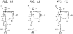
- FIGS. 1A, 1B, and 1C illustrate a temperature detection method of a semiconductor element according to Embodiment 1.
- a half bridge circuit 20 comprised of insulated-gate field effect transistors (FETs) Tr1 and Tr2 as a semiconductor element is exemplified.
- the half bridge circuit 20 configures at least a part of a power conversion device for example, and is controlled by pulse width modulation.
- the half bridge circuit 20 is comprised of the field effect transistor Tr1 coupled between a high potential node 21 and a coupling node U, and the field effect transistor Tr2 coupled between the coupling node U and a ground node 22.
- a high potential VH is supplied to the high potential node 21, and a ground potential GND is supplied to the ground node 22.
- An inductor 23 as a load is coupled between the coupling node U and the high potential node 21.
- each of the field effect transistor Tr1 and the field effect transistor Tr2 is an N-type MISFET (Metal Insulator Semiconductor FET).
- the MISFET includes an MOSFET (Metal Oxide Semiconductor FET) of which the insulator is formed with an oxide. Therefore, a drain electrode (D) of the field effect transistor Tr1 is coupled to the high potential node 21, and a source electrode (S) of the field effect transistor Tr1 is coupled to the coupling node U.
- a drain electrode (D) of the field effect transistor Tr2 is coupled to the coupling node U, and a source electrode (S) of the field effect transistor Tr2 is coupled to the ground node 22 via a shunt resistor RES.
- a circulating current 102 (also called a regenerative current) flows from the high potential node 21, passing an inductor 23 and a body diode of the field effect transistor Tr1 in order, and reaching the high potential node 21 again.
- the body diode will be explained in detail with reference to FIG. 2 and FIG. 3 .
- the field effect transistor Tr1 is set to an ON state from the state of FIG. 1B .
- a circulating current 103 flows from the high potential node 21, passing the inductor 23 and a channel region of the field effect transistor Tr1 in order, and reaching the high potential node 21 again.
- the state illustrated in FIG. 1A and the state illustrated in FIG. 1C are repeated alternately. In this case, it is necessary to prevent a flow-through current from flowing between the high potential node 21 and the ground node 22 via the field effect transistors Tr1 and Tr2 both in an ON state. Therefore, the state illustrated in FIG. 1B is inserted between the state illustrated in FIG. 1A and the state illustrated in FIG. 1C .
- the state illustrated in FIG. 1B is a period called "dead time.”
- the voltage between a source and a drain of the field effect transistor (that is, a forward voltage between an anode and a cathode of the body diode) is detected in this dead time (that is, in the state when a circulating current flows through the body diode).
- the forward voltage of the body diode decreases as the temperature rises. Therefore, by detecting the forward voltage of the body diode, it is possible to detect correctly the junction temperature of the semiconductor element.
- the forward voltage of the body diode is detected in the dead time in process of shifting from the state where the energization current 101 illustrated in FIG. 1A flows to the state where the circulating current 103 illustrated in FIG. 1C flows.
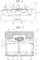
- FIG. 2 explains about a horizontal-type MISFET
- FIG. 3 explains about a vertical-type MISFET.
- FIG. 2 is a sectional view illustrating an example of the configuration of a horizontal-type MISFET.
- the horizontal-type MISFET 30 is comprised of a P-type semiconductor substrate 31, a P-type diffusion region (P-well) 32 formed in a part of the upper part of the P-type semiconductor substrate 31, and N-type impurity regions 33 and 34 formed in a part of the upper part of the P-type diffusion region 32.
- a body diode 36 is formed by the P-type diffusion region 32 and the N-type impurity region 33.
- the horizontal-type MISFET 30 is further comprised of a drain electrode D formed over the surface of the N-type impurity region 33, a source electrode S formed over the surface of the N-type impurity region 34, a gate electrode G formed between the drain electrode D and the source electrode S, and a back gate electrode BG formed over the surface of the P-type diffusion region 32.
- the gate electrode G is coupled to the surface of the P-type diffusion region 32 and the surface of the N-type impurity regions 33 and 34, through the intervention of a gate insulating film 35.
- the source electrode S and the back gate electrode BG are mutually coupled via wiring.
- the energization current 101 flows from the drain electrode D to the source electrode S, passing the N-type impurity region 33, the N-type channel region formed in the upper part of the P-type diffusion region 32, and the N-type impurity region 34 in order.
- the circulating current 103 flows from the source electrode S to the drain electrode D, passing the N-type impurity region 34, the N-type channel region, and the N-type impurity region 33 in order.
- the circulating current 102 can flow in the direction from the back gate electrode BG to the drain electrode D, passing the P-type diffusion region 32 and the N-type impurity region 33 in order. Therefore, it is possible to detect the junction temperature of the horizontal-type MISFET 30 by detecting the source-drain voltage of the horizontal-type MISFET 30 (that is, the forward voltage of the body diode 36) in the state where this circulating current 102 is flowing.
- FIG. 3 is a sectional view illustrating an example of the configuration of a vertical-type MISFET.
- the vertical-type MISFET 40 is comprised of a high-concentration N(+)-type drain layer 44, a low-concentration N(-) -type drift layer 43 formed in the upper part of the N(+)-type drain layer 44, a P-type base layer 42 formed in a part of the upper part of the N(-) -type drift layer 43, and a high-concentration N(+) -type source layer 41 formed in a part of the upper part of the P-type base layer 42.
- a body diode 46 is formed by the P-type base layer 42 and the N(-) -type drift layer 43.
- a gate electrode G is formed over a part of the surface of the N(+) -type source layer 41, a part of the surface of the P-type base layer 42, and a part of the surface of the N(-) -type drift layer 43, with the intervention of the gate insulating film 45.
- a source electrode S is formed over a part of the surface of the N (+) -type source layer 41 and a part of the surface of the P-type base layer 42.
- a drain electrode D is formed over the surface of the N(+) -type drain layer 44 on the opposite side of the source electrode S.
- an energization current 101 flows from the drain electrode D to the source electrode, passing the N(+) -type drain layer 44, the N(-) -type drift layer 43, the N-type channel region of the upper part of the P-type base layer 42, and the N(+)-type source layer 41 in order.
- the circulating current 103 flows from the source electrode S to the drain electrode D, passing the N(+)-type source layer 41, the N-type channel region of the upper part of the P-type base layer 42, the N(-) -type drift layer 43, and the N(+) -type drain layer 44 in order.
- the circulating current 102 can flow in the direction from the source electrode S to the drain electrode D, passing the P-type base layer 42, the N(-) -type drift layer 43, and the N(+) -type drain layer 44. Therefore, it is possible to detect the junction temperature of the vertical-type MISFET 40 by detecting the source-drain voltage of the vertical-type MISFET 40 (that is, the forward voltage of the body diode 46) in the state where this circulating current 102 is flowing.
- FIG. 4 is a block diagram illustrating the configuration of the semiconductor device according to Embodiment 1.
- the semiconductor device 50A illustrated in FIG. 4 controls ON/OFF of the field effect transistors Tr1 and Tr2 that configure the half bridge circuit 20, and detects the anode-cathode voltage of the body diode of the field effect transistor Tr1.
- the half bridge circuit 20 configures at least a part of the power conversion device.
- the half bridge circuit 20 and the semiconductor device 50A may configure a part of the power modules.
- a load current IU flowing in the direction from a coupling node U of the half bridge circuit 20 to the load 23 is defined as positive. Therefore, the sign of the energization current 101 illustrated in FIG. 1A (that is, the electric current flowing in the direction from the load 23 to the coupling node U of the half bridge circuit 20) is negative.
- the semiconductor device 50A is comprised of a gate driving circuit 51 on the high potential side, a gate driving circuit 52 on the low potential side, a differential amplifier 53, a sample hold circuit 54, an A/D (Analog to Digital) converter 55, a controller 56, and a switch 57.
- the gate driving circuit 51 receives a gate control signal VT from the controller 56.
- the gate driving circuit 51 converts a reference potential of the gate control signal VT from the ground potential GND to a potential VU of the coupling node U, and amplifies the signal level of the gate control signal VT to generate a drive voltage to be supplied to a gate electrode G1 of the high-potential-side field effect transistor Tr1.
- ON/OFF of the field effect transistor Tr1 is controlled by the drive voltage supplied to the gate electrode G1 from the gate driving circuit 51.
- the gate driving circuit 52 amplifies a gate control signal VB received from the controller 56 to generate a drive voltage to be supplied to a gate electrode G2 of the low-potential-side field effect transistor Tr2. ON/OFF of the field effect transistor Tr2 is controlled by the drive voltage supplied to the gate electrode G2 from the gate driving circuit 52.
- the differential amplifier 53 has input nodes IN1 and IN2, and an output node OT.
- the input node IN1 is coupled to the coupling node U via the switch 57 that switches ON/OFF. Accordingly, the potential VU of the coupling node U is fetched into the input node IN1.
- the input node IN2 is coupled to the high potential node 21 and fetches the potential VH of the high potential node 21.
- the output node OT is coupled to the sample hold circuit 54.
- the differential amplifier 53 outputs, from the output node OT, a voltage signal proportional to the potential difference between the input node IN1 and the input node IN2.
- FIG. 4 illustrates an example the differential amplifier 53 comprised of an operational amplifier. As illustrated in FIG. 4 , the differential amplifier 53 is comprised of an operational amplifier 65 and resistive elements 61, 62, 63, and 64.
- the resistive element 61 is coupled between the input node IN2 and the (-) terminal of the operational amplifier 65.
- the resistive element 62 is coupled between the (-) terminal and an output terminal of the operational amplifier 65 (the output terminal is directly coupled to the output node OT).
- the resistive element 63 is coupled between the input node IN1 and the (+) terminal of the operational amplifier 65.
- One end of the resistive element 64 is coupled to the (+) terminal of the operational amplifier 65, and the other end of the resistive element 64 is supplied with a reference voltage Vref on the basis of the ground potential GND.
- a terminal 58 for fetching the ground potential GND is provided in the semiconductor device 50A.
- the terminal 58 is coupled to a coupling node of the field effect transistor Tr2 and a shunt resistor RES (hereinafter the coupling node is called a low potential node 24).
- Vtemp VU ⁇ VH ⁇ R 2 / R 1 + Vref
- the sample hold circuit 54 is comprised of a switch 70 that switches ON/OFF and a capacitor 71.
- One end of the switch 70 is coupled to the output node OT of the differential amplifier 53, and the other end of the switch 70 is coupled to one end of the capacitor 71.
- the other end of the capacitor 71 is supplied with the ground potential GND.
- the other end of the switch 70 is further coupled to the A/D converter 55.
- the A/D converter 55 performs digital conversion of a voltage Vtemp held by the capacitor 71 of the sample hold circuit 54 and outputs the A/D-converted voltage Vtemp to the controller 56.
- the controller 56 generates the gate control signals VT and VB, a control signal CTL1 for controlling ON/OFF of the switch 70 of the sample hold circuit 54, and a control signal CTL2 for controlling ON/OFF of the switch 57.
- the controller 56 performs protected operation, such as setting to OFF all the field effect transistors Tr1 and Tr2, when the voltage Vtemp reaches an upper limit.
- the controller 56 may be configured with a microcomputer including a CPU (Central Processing Unit) and a memory, or may be configured with an FPGA (Field Programmable Gate Array), or may be configured with an exclusive-use circuit. Alternatively, the controller 56 may be configured by combining these circuits arbitrarily.
- a microcomputer including a CPU (Central Processing Unit) and a memory
- FPGA Field Programmable Gate Array
- the controller 56 may be configured by combining these circuits arbitrarily.
- FIG. 5 is a timing chart illustrating operation of the semiconductor device illustrated in FIG. 4 .
- FIG. 5 illustrates schematically, from the top, the waveforms of the gate control signals VT and VB, the control signals CTL1 and CTL2, and the potential VU at the coupling node U.
- the operation of the semiconductor device 50A illustrated in FIG. 4 is explained.
- the controller 56 sets the gate control signal VT at the H level and the gate control signal VB at the L level. According to this setting, the high-potential-side field effect transistor Tr1 is controlled in the ON state, and the low-potential-side field effect transistor Tr2 is controlled in the OFF state. As a result, the potential VU of the coupling node U becomes equal to the potential VH of the high potential node 21. It is assumed that, at the point of Time t1, the circulating current 103 illustrated in FIG. 1 has attenuated to 0.
- the controller 56 sets the control signals CTL1 and CTL2 at the L level. Accordingly, the switch 70 of the sample hold circuit 54 and the switch 57 are set in the OFF state.
- the controller 56 sets the gate control signal VT at the L level and the gate control signal VB at the H level. According to this setting, the field effect transistor Tr1 is controlled in the OFF state, and the field effect transistor Tr2 is controlled in the ON state. As a result, the potential VU of the coupling node U falls to the ground potential GND. During this Period T11, the energization current 101 illustrated in FIG. 1A flows, and the magnitude of the current increases gradually.
- the controller 56 switches the gate control signal VB from the H level to the L level.
- the low-potential-side field effect transistor Tr2 changes from the ON state to the OFF state, and the potential VU of the coupling node U rises from the ground potential GND.
- the field effect transistors Tr1 and Tr2 are both maintained in the OFF state.
- the circulating current 102 illustrated in FIG. 1B flows through the body diode of the field effect transistor Tr1.
- the potential VU of the coupling node U finally reaches a value that is higher than the potential VH of the high potential node 21, by the forward voltage Vf of the body diode.
- the controller 56 sets the control signals CTL1 and CTL2 at the H level, to set the switch 70 of the sample hold circuit 54 and the switch 57 in the ON state.
- the source-drain voltage of the field effect transistor Tr1 (that is, the forward voltage Vf of the body diode) is detected by the differential amplifier 53.
- the voltage Vtemp outputted from the differential amplifier 53 is sampled by the sample hold circuit 54 and is held by the capacitor 71.
- the controller 56 detects the junction temperature of the field effect transistor Tr1 based on the voltage Vtemp held by the capacitor 71.
- the voltage detected changes corresponding to the electric current flowing through the body diode. Therefore, it is necessary to control the magnitude of the energization current 101 at Time t2 immediately before being switched to Period T12, to a predetermined value. This value can be adjusted by the length of Period T11 (that is, the duty factor corresponding to a carrier frequency).
- the controller 56 switches the gate control signal VT from the L level to the H level.
- the state of the high-potential-side field effect transistor Tr1 changes from the OFF state to the ON state. Therefore, as illustrated in FIG. 1C , FIG. 2, and FIG. 3 , the path of the circulating current changes to the path (103) that passes the N-type channel region of the field effect transistor Tr1.
- the controller 56 switches the control signals CTL1 and CTL2 from the H level to the L level, to terminate the sampling of the source-drain voltage of the field effect transistor Tr1.
- Period T13 from Time t4 to Time t5 the field effect transistor Tr1 is maintained in the ON state, and the field effect transistor Tr2 is maintained in the OFF state.
- the controller 56 switches the gate control signal VT from the H level to the L level. According to this switching, the state of the high-potential-side field effect transistor Tr1 changes from the ON state to the OFF state. Therefore, as illustrated in FIG. 1B , FIG. 2, and FIG. 3 , the path of the circulating current changes to the path (102) that passes the body diode. During Period T14 from Time t5 to Time t6, the field effect transistors Tr1 and Tr2 are both maintained in the OFF state.
- Period T14 Different from the case of Period T12, in Period T14, the sampling of the source-drain voltage of the field effect transistor Tr1 is not performed.
- the circulating current gradually attenuates in Periods T12, T13, and T14 (it attenuates to 0 depending on conditions) ; accordingly, it is difficult to make a precise measurement of the forward voltage Vf of the body diode in Period T14. This is the reason of not performing the sampling in Period T14. Therefore, the detection of the junction temperature of the field effect transistor is performed at a time of changing from the energization period to supply the electric power to the load from the power supply to the regeneration period.
- Periods T11 to T14 correspond to one cycle of the PWM signal. Periods T21 to T24 as the next one cycle correspond to Periods T11 to T14, respectively, and the same control is repeated. Therefore, the change of the load current IU in Periods T21 to T24 is the same as the change of the load current IU in Periods T11 to T14.
- the load current IU that is 0 at the start time (Time t1) of Period T11 illustrated in FIG. 5 increases in the energization period T11 (from Time t1 to t2), and decreases gradually in the regeneration periods T12, T13, and T14 (from Time t3 to t6). Then, at the end of Period T14 (Time t6), the load current IU starts to increase again. The load current IU increases again in the energization period T21, and decreases gradually in the regeneration periods T22, T23, and T24.
- the control signals CTL1 and CTL2 are set to the H level, to perform remeasurement of the forward voltage Vf of the body diode.
- the remeasurement described above may be performed several times. In this case, the value obtained by averaging the measurement results of several times may be determined as the final forward voltage Vf.
- the forward voltage Vf When the forward voltage Vf is remeasured as shown in FIG. 5 , it is desirable to make the measuring condition of the forward voltage Vf the same, in the first measurement in Period T12 and the second measurement in Period T22. Specifically, in order to set the initial value of the load current IU to 0 at the start time (Time t1) of the energization period T11 and at the start time (Time t6) of the energization period T21, it is desirable for the load current IU to attenuate to 0 in the regeneration periods T12, T13, and T14.
- the junction temperature of the power MISFET is measured based on the temperature characteristic of the body diode of the power MISFET. Therefore, it is possible to measure the junction temperature of the MISFET more accurately than the method used in the past. It is not necessary to employ sensors, such as a thermistor or a diode, for the temperature detection; accordingly, it is possible to reduce the number of parts that configure the system compared with the past.
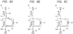
- FIGS. 6A, 6B, and 6C illustrate the temperature detection method of the semiconductor element according to the modified example of Embodiment 1.
- the explanatory drawings illustrated in FIGS. 6A, 6B, and 6C correspond to the explanatory drawings illustrated in FIGS. 1A, 1B, and 1C , and illustrate the half bridge circuit 20 comprised of the field effect transistors Tr1 and Tr2.
- the half bridge circuit 20 may be considered to configure at least a part of the power conversion device. In the case of FIGS.
- the inductor 23 as the load is coupled in parallel with the field effect transistor Tr2, between the coupling node U and the low potential node 24 (the low potential node 24 is a coupling node of the field effect transistor Tr2 and the shunt resistor RES).
- the field effect transistor Tr1 is set to an OFF state from the state of FIG. 6A .
- the circulating current 102 flows from the coupling node U, passing the inductor 23, the low potential node 24, and the body diode of the field effect transistor Tr2 in order, and reaching the coupling node U again.
- the field effect transistor Tr2 is set to an ON state from the state of FIG. 1B .
- the circulating current 103 flows from the coupling node U, passing the inductor 23, the low potential node 24, the N-type channel region of the field effect transistor Tr2 in order, and reaching the coupling node U again.
- the state illustrated in FIG. 6A and the state illustrated in FIG. 6C are repeated alternately. In this case, it is necessary to prevent a flow-through current from flowing between the high potential node 21 and the ground node 22 via the field effect transistors Tr1 and Tr2, both in an ON state. Therefore, the state illustrated in FIG. 6B , that is the period of so-called dead time, is inserted between the state illustrated in FIG. 6A and the state illustrated in FIG. 6C .
- the source-drain voltage of the field effect transistor Tr2 (that is, the forward voltage between the anode and the cathode of the body diode) is detected. Then, based on the temperature characteristic of the body diode, the junction temperature of the field effect transistor Tr2 is detected.
- FIG. 7 is a block diagram illustrating the configuration of the semiconductor device according to the modified example of Embodiment 1.
- a semiconductor device 50B illustrated in FIG. 7 is different from the semiconductor device 50A illustrated in FIG. 4 in the connection of the differential amplifier 53.
- the input node IN1 of the differential amplifier 53 is coupled to the low potential node 24 via the terminal 58.
- the input node IN2 of the differential amplifier 53 is coupled to the coupling node U via the switch 57.
- the other configurations illustrated in FIG. 7 are the same as those illustrated in FIG. 4 . Therefore, the same reference number or symbol is given to the same or corresponding part, and the explanation thereof is not repeated.
- FIG. 8 is a timing chart illustrating operation of the semiconductor device illustrated in FIG. 7 .
- the timing chart illustrated in FIG. 8 corresponds to the timing chart illustrated in FIG. 5 .
- FIG. 8 illustrates schematically, from the top, the waveforms of the gate control signals VT and VB, the control signals CTL1 and CTL2, and the potential VU at the coupling node U.
- FIG. 7 and FIG. 8 mainly, the operation of the semiconductor device 50B illustrated in FIG. 7 is explained.
- the controller 56 sets the gate control signal VT at the L level and the gate control signal VB at the H level. According to this setting, the high-potential-side field effect transistor Tr1 is controlled in the OFF state and the low-potential-side field effect transistor Tr2 is controlled in the ON state. As a result, the potential VU of the coupling node U becomes equal to the potential of the low potential node 24 (nearly the ground potential GND). It is assumed that, at the point of Time t1, the circulating current 103 illustrated in FIG. 6 has attenuated to 0.
- the controller 56 sets the control signals CTL1 and CTL2 at the L level. Accordingly, the switch 70 of the sample hold circuit 54 and the switch 57 are set in the OFF state.
- the controller 56 sets the gate control signal VT at the H level and the gate control signal VB at the L level. According to this setting, the field effect transistor Tr1 is controlled in the ON state, and the field effect transistor Tr2 is controlled in the OFF state. As a result, the potential VU of the coupling node U rises to the potential VH of the high potential node 21. During this Period T11, the energization current 101 illustrated in FIG. 6A flows, and the magnitude of the current increases gradually.
- the controller 56 switches the gate control signal VT from the H level to the L level. According to this switching, the high-potential-side field effect transistor Tr1 changes from the ON state to the OFF state, and the potential VU of the coupling node U falls from the potential VH of the high potential node 21.
- the field effect transistors Tr1 and Tr2 are both maintained in the OFF state.
- the circulating current 102 illustrated in FIG. 6B flows through the body diode of the field effect transistor Tr2.
- the potential VU of the coupling node U finally reaches a value that is lower than the potential of the low potential node 24 (that is, the ground potential GND), by the forward voltage Vf of the body diode.
- the controller 56 From Time t3 after the lapse of the prescribed period of time from Time t2 to Time t4, the controller 56 sets the control signals CTL1 and CTL2 at the H level, to set the switch 70 of the sample hold circuit 54 and the switch 57 in the ON state.
- the source-drain voltage of the field effect transistor Tr2 (that is, the forward voltage Vf of the body diode) is detected by the differential amplifier 53 .
- the voltage Vtemp outputted from the differential amplifier 53 is sampled by the sample hold circuit 54 and is held by the capacitor 71.
- the controller 56 detects the junction temperature of the field effect transistor Tr2 based on the voltage Vtemp held by the capacitor 71.
- the controller 56 switches the gate control signal VB from the L level to the H level. According to this switching, the low-potential-side field effect transistor Tr2 changes from the OFF state to the ON state. Therefore, as illustrated in FIG. 6C , FIG. 2, and FIG. 3 , the path of the circulating current changes to the path (103) that passes the N-type channel region of the field effect transistor Tr2.
- the controller 56 switches the control signals CTL1 and CTL2 from the H level to the L level, to terminate the sampling of the source-drain voltage of the field effect transistor Tr2.
- Period T13 from Time t4 to Time t5 the field effect transistor Tr1 is maintained in the OFF state, and the field effect transistor Tr2 is maintained in the ON state.
- the controller 56 switches the gate control signal VB from the H level to the L level. According to this switching, the low-potential-side field effect transistor Tr2 changes from the ON state to the OFF state. Therefore, as illustrated in FIG. 6B , FIG. 2, and FIG. 3 , the path of the circulating current changes to the path (102) that passes the body diode.
- the field effect transistors Tr1 and Tr2 are both maintained in the OFF state. Different from the case of Period T12, in Period T14, the sampling of the source-drain voltage of the field effect transistor Tr1 is not performed.
- Periods T11 to T14 correspond to one cycle of the PWM signal.
- Periods T21 to T24 correspond to Periods T11 to T14, respectively, and the same control is repeated.
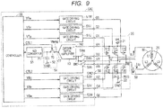
- Embodiment 2 the explanation is made for an example in which a motor-controlling inverter device 25 as a power conversion device is controlled by a semiconductor device 50C.
- FIG. 9 is a block diagram illustrating the configuration of the semiconductor device according to Embodiment 2.
- the semiconductor device 50C illustrated in FIG. 9 controls ON/OFF of field effect transistors Tr1 to Tr6 that configure the inverter device 25 (also called a three-phase bridge circuit) as the power conversion device, and detects the cathode-to-anode voltage of a body diode of the field effect transistors Tr1, Tr3, and Tr5 of the upper arm.
- the semiconductor device 50C and the inverter device 25 may be configured as a part of the power module.
- the three-phase motor M is a three-phase synchronous motor or a brushless DC motor.
- the three-phase motor M includes star-connected stator windings L1, L2, and L3.
- the inverter device 25 is comprised of the field effect transistors Tr1 and Tr2 for generating a U-phase motor current IU, the field effect transistors Tr3 and Tr4 for generating a V-phase motor current IV, and the field effect transistors Tr5 and Tr6 for generating a W-phase motor current IW.
- the field effect transistors Tr1 to Tr6 are all N-type MISFETs.
- the field effect transistor Tr1 is coupled between the high potential node 21 and the coupling node U, and the field effect transistor Tr2 is coupled between the coupling node U and the low potential node 24.
- the coupling node U is coupled to one end of the stator winding L1, and the other end of the stator winding L1 is coupled to a neutral point 26.
- the low potential node 24 is coupled to the ground node 22 via the shunt resistor RES.
- the field effect transistor Tr3 is coupled between the high potential node 21 and a coupling node V
- the field effect transistor Tr4 is coupled between the coupling node V and the low potential node 24.
- the coupling node V is coupled to one end of the stator winding L2, and the other end of the stator winding L2 is coupled to the neutral point 26.
- the field effect transistor Tr5 is coupled between the high potential node 21 and a coupling node W
- the field effect transistor Tr6 is coupled between the coupling node W and the low potential node 24.
- the coupling node W is coupled to one end of the stator winding L3, and the other end of the stator winding L3 is coupled to the neutral point 26.
- the Semiconductor device 50C is comprised of high-potential-side gate driving circuits 51U, 51V, and 51W, low-potential-side gate driving circuits 52U, 52V, and 52W, a differential amplifier 53, a sample hold circuit 54, an A/D (Analog to Digital) converter 55, a controller 56, and switches SWa, SWb, and SWc.
- the gate driving circuit 51U receives a gate control signal VTu from the controller 56.
- the gate driving circuit 51U converts a reference potential of the gate control signal VTu from the ground potential GND to a potential VU of the coupling node U, and amplifies the signal level of the gate control signal VTu to generate a drive voltage to be supplied to a gate electrode G1 of the high-potential-side field effect transistor Tr1.
- ON/OFF of the field effect transistor Tr1 is controlled by the drive voltage supplied to the gate electrode G1 from the gate driving circuit 51U.
- the gate driving circuit 51V receives a gate control signal VTv from the controller 56.
- the gate driving circuit 51V converts a reference potential of the gate control signal VTv from the ground potential GND to a potential VV of the coupling node V, and amplifies the signal level of the gate control signal VTv to generate a drive voltage to be supplied to a gate electrode G3 of the high-potential-side field effect transistor Tr3. ON/OFF of the field effect transistor Tr3 is controlled by the drive voltage supplied to the gate electrode G3 from the gate driving circuit 51V.
- the gate driving circuit 51W receives a gate control signal VTw from the controller 56.
- the gate driving circuit 51W converts a reference potential of the gate control signal VTw from the ground potential GND to a potential VW of the coupling node W, and amplifies the signal level of the gate control signal VTw to generate a drive voltage to be supplied to a gate electrode G5 of the high-potential-side field effect transistor Tr5.
- ON/OFF of the field effect transistor Tr5 is controlled by the drive voltage supplied to the gate electrode G5 from the gate driving circuit 51W.
- the gate driving circuit 52U amplifies a gate control signal VBu received from the controller 56 to generate a drive voltage to be supplied to a gate electrode G2 of the low-potential-side field effect transistor Tr2. ON/OFF of the field effect transistor Tr2 is controlled by the drive voltage supplied to the gate electrode G2 from the gate driving circuit 52U.
- the gate driving circuit 52V amplifies a gate control signal VBv received from the controller 56 to generate a drive voltage to be supplied to a gate electrode G4 of the low-potential-side field effect transistor Tr4. ON/OFF of the field effect transistor Tr4 is controlled by the drive voltage supplied to the gate electrode G4 from the gate driving circuit 52V.
- the gate driving circuit 52W amplifies a gate control signal VBw received from the controller 56 to generate a drive voltage to be supplied to a gate electrode G6 of the low-potential-side field effect transistor Tr6. ON/OFF of the field effect transistor Tr6 is controlled by the drive voltage supplied to the gate electrode G6 from the gate driving circuit 52W.
- the differential amplifier 53 has the same configuration as the differential amplifier 53 explained in FIG. 4 .
- the differential amplifier 53 outputs, from the output node OT, a voltage signal proportional to the potential difference between the input node IN1 and the input node IN2.
- the input node IN1 of the differential amplifier 53 is coupled to the coupling node U via the switch SWa that switches ON/OFF and can fetch the potential VU of the coupling node U.
- the input node IN1 of the differential amplifier 53 is coupled to the coupling node V via the switch SWb that switches ON/OFF and can fetch the potential W of the coupling node V.
- the input node IN1 of the differential amplifier 53 is coupled to the coupling node W via the switch SWc that switches ON/OFF and can fetch the potential VW of the coupling node W.
- the input node IN2 is coupled to the high potential node 21 and fetches the potential VH of the high potential node 21.
- the output node OT is coupled to the sample hold circuit 54.
- the differential amplifier 53 outputs, from the output node OT, a voltage signal proportional to the potential difference between the input node IN1 and the input node IN2.
- the configuration of the sample hold circuit 54 is the same as in FIG. 4 ; therefore, the explanation thereof is not repeated.
- the A/D converter 55 performs digital conversion of a voltage Vtemp held by the capacitor 71 of the sample hold circuit 54 and outputs the A/D-converted voltage Vtemp to the controller 56.
- the controller 56 generates the gate control signals VTu, VTv, VTw, VBu, VBv, and VBw, the control signal CTL1 for controlling ON/OFF of the switch 70 of the sample hold circuit 54, and the control signal CTL2 for controlling ON/OFF of the switches SWa, SWb, and SWc. Furthermore, the controller 56 performs protected operation, such as turning off all the field effect transistors Tr1 to Tr6, when the voltage Vtemp reaches an upper limit.
- the three-phase motor M is driven by the 2-phase excitation method in which an electric current is made to flow only through two phases.
- two phases through which the motor current flows are switched for every electrical angle of 60 degrees by the inverter device 25.
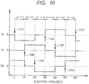
- FIG. 10 illustrates switching of energized phases of the motor current.
- the horizontal axis of FIG. 10 indicates an electrical angle, and the vertical axis indicates the magnitude of the motor currents IU, IV, and IW schematically.
- the sign of the motor currents IU, IV, and IW is defined as positive.
- the inverter device 25 is PWM-controlled to make the motor current flow in the direction from the stator winding L3 to the stator winding L1. Therefore, the value of the motor current IU is negative, the value of the motor current IV is 0, and the value of the motor current IW is positive.
- the inverter device 25 is PWM-controlled to make the motor current flow in the direction from the stator winding L2 to the stator winding L1. Therefore, the value of the motor current IU is negative, the value of the motor current IV is positive, and the value of the motor current IW is 0.
- the inverter device 25 is PWM-controlled to make the motor current flow in the direction from the stator winding L2 to the stator winding L3. Therefore, the value of the motor current IU is 0, the value of the motor current IV is positive, and the value of the motor current IW is negative.
- the inverter device 25 is PWM-controlled to make the motor current flow in the direction from the stator winding L1 to the stator winding L3. Therefore, the value of the motor current IU is positive, the value of the motor current IV is 0, and the value of the motor current IW is negative.
- the inverter device 25 is PWM-controlled to make the motor current flow in the direction from the stator winding L1 to the stator winding L2. Therefore, the value of the motor current IU is positive, the value of the motor current IV is negative, and the value of the motor current IW is 0.
- the inverter device 25 is PWM-controlled to make the motor current flow in the direction from the stator winding L3 to the stator winding L2. Therefore, the value of the motor current IU is 0, the value of the motor current IV is negative, and the value of the motor current IW is positive.
- the junction temperature can be detected without practically affecting the drive control of the three-phase motor M. This is because, in the state immediately after starting energization to a stator winding that is not energized until now, the magnitude of the electric current flowing through the stator winding concerned can be controlled to a current value (for example, about 1 to 2A) that is smaller than the current value in the steady state.
- the small current value in this case is adjusted to a value suitable for the measurement of the forward voltage Vf of the body diode.
- the detection of the junction temperature of the field effect transistor is performed at a time of changing to the regeneration period from the energization period to supply the electric power to the load from the power supply.
- the following explains specifically the case of detecting the junction temperature of the field effect transistor Tr1 of the upper arm of the U phase directly coupled to the stator winding L1.
- the dead time after switching the field effect transistor Tr2 from the ON state to the OFF state first until switching the field effect transistor Tr1 from the OFF state to the ON state is used for detection of the junction temperature.
- the dead time after switching the field effect transistor Tr1 from the ON state to the OFF state first until switching the field effect transistor Tr2 from the OFF state to the ON state is used for detection of the junction temperature.
- the following explains the case of detecting the junction temperature of the field effect transistor Tr3 of the upper arm of the V phase directly coupled to the stator winding L2.
- the timing 112P at 240 degrees of the electrical angle in FIG. 10
- the dead time after switching the field effect transistor Tr4 from the ON state to the OFF state first until switching the field effect transistor Tr3 from the OFF state to the ON state is used for detection of the junction temperature.
- the dead time after switching the field effect transistor Tr3 from the ON state to the OFF state first until switching the field effect transistor Tr4 from the OFF state to the ON state is used for detection of the junction temperature.
- the following explains the case of detecting the junction temperature of the field effect transistor Tr5 of the upper arm of the W phase directly coupled to the stator winding L3.
- the timing 113P at 120 degrees of the electrical angle in FIG. 10
- the dead time after switching the field effect transistor Tr6 from the ON state to the OFF state first until switching the field effect transistor Tr5 from the OFF state to the ON state is used for detection of the junction temperature.
- the dead time after switching the field effect transistor Tr5 from the ON state to the OFF state first until switching the field effect transistor Tr6 from the OFF state to the ON state is used for detection of the junction temperature.
- FIGS. 11A, 11B, and 11C illustrate the concrete example of the temperature detection method of the field effect transistor according to Embodiment 2.
- FIG. 11A illustrates the case where the field effect transistors Tr1 and Tr4 are in the ON state and the field effect transistors Tr2, Tr3, Tr5, and Tr6 are in the OFF state.
- the motor current flows through the high-potential-side field effect transistor Tr1, the stator winding L1, the stator winding L2, and the low-potential-side field effect transistor Tr4 in order.
- the field effect transistor Tr4 is set to an OFF state from the state of FIG. 11A .
- the circulating current also called a regenerative current
- the high-potential-side field effect transistor Tr1 flows through the high-potential-side field effect transistor Tr1, the stator winding L1, the stator winding L2, and the body diode of the high-potential-side field effect transistor Tr3 in order. Therefore, it is possible to detect the junction temperature of the field effect transistor Tr3, based on the temperature characteristic of the body diode.
- the field effect transistor Tr3 is set to an ON state from the state of FIG. 11B .
- the circulating current (regenerative current) flows through the high-potential-side field effect transistor Tr1, the stator winding L1, the stator winding L2, and the channel region of the high-potential-side field effect transistor Tr3.
- FIG. 12 is a timing chart illustrating the temperature detection procedure of the field effect transistor according to Embodiment 2.
- FIG. 12 illustrates schematically the waveform of the control signals and the waveform of the potential VV of the coupling node V in the neighborhood of the timing 112P (240 degrees of the electrical angle) illustrated in FIG. 10 .
- the operation of the semiconductor device 50C in case of detecting the junction temperature of the field effect transistor Tr3 is explained.
- the controller 56 controls the inverter device 25 to make the energization current flow in the direction from the stator winding L1 to the stator winding L3.
- the controller 56 sets the gate control signals VTu and VBw at the H level, and sets the gate control signals VBu, VTv, VBv, and VTw at the L level.
- the motor current flows through the field effect transistor Tr1, the stator winding L1, the stator winding L3, and the field effect transistor Tr6 in order.
- the controller 56 switches the gate control signal VBv from the L level to the H level, and switches the gate control signal VBw from the H level to the L level. According to this switching, the low-potential-side field effect transistor Tr4 of the V phase changes from the OFF state to the ON state, and the low-potential-side field effect transistor Tr6 of the W phase changes from the ON state to the OFF state. As a result, the potential W of the coupling node V falls to the ground potential GND.
- the state of the control signal described above is maintained during Period T11 from Time t1 to Time t2. Therefore, during Period T11, the motor current (that is, the energization current) flows in the direction from the stator winding L1 to the stator winding L2 as illustrated in FIG. 11A , and the value of the electric current flowing through the stator winding L2 increases from 0 gradually. Although not illustrated in FIG. 11A , the electric current that has been flowing through the stator winding L3 in the immediately preceding period of Time t1 flows through the body diode of the field effect transistor Tr5 as the circulating current, and the current value thereof decreases gradually.
- the controller 56 switches the gate control signal VBv from the H level to the L level.
- the low-potential-side field effect transistor Tr4 of the V phase changes from the ON state to the OFF state, and the potential W of the coupling node V rises from the ground potential GND.
- the state of the control signal described above is maintained during Period T12 from Time t2 to Time t4. Therefore, the circulating current illustrated in FIG. 11B flows during Period T12. This circulating current flows through the body diode of the field effect transistor Tr3. Therefore, the potential VV of the coupling node V finally reaches a value that is higher than the potential VH of the high potential node 21, by the forward voltage Vf of the body diode.
- the forward voltage Vf of the body diode of the field effect transistor Tr3 is detected in the period from Time t3 after a prescribed period of time from Time t2, to Time t4.
- the controller 56 controls the control signals CTL1 and CTL2 to set the switch 70 of the sample hold circuit 54 and the switch SWb in the ON state.
- the source-drain voltage of the field effect transistor Tr3 (that is, the forward voltage Vf of the body diode) is detected by the differential amplifier 53.
- the voltage Vtemp outputted from the differential amplifier 53 is sampled by the sample hold circuit 54 and is held by the capacitor 71.
- the controller 56 detects the junction temperature of the field effect transistor Tr3 based on the voltage Vtemp held by the capacitor 71.
- the voltage detected changes corresponding to the electric current flowing through the body diode. Therefore, it is necessary to control the magnitude of the motor current IV flowing through the stator winding L2 at Time t2 immediately before being switched to Period T12, to a predetermined value. This value can be adjusted by the length of Period T11 (that is, the duty factor corresponding to a carrier frequency).
- the controller 56 switches the gate control signal VTv from the L level to the H level. According to this switching, the state of the high-potential-side field effect transistor Tr3 changes from the OFF state to the ON state. Therefore, as illustrated in FIG. 11C , the path of the circulating current changes to the path (103 in FIG. 2 and FIG. 3 ) that passes the N-type channel region of the field effect transistor Tr3.
- the controller 56 controls the control signals CTL1 and CTL2, to terminate the sampling of the source-drain voltage of the field effect transistor Tr3. The state of the control signal outputted from the controller 56 is maintained during Period T13 from Time t4 to Time t5.
- the controller 56 switches the gate control signal VTv from the H level to the L level. According to this switching, the high-potential-side field effect transistor Tr3 changes from the ON state to the OFF state. Therefore, as illustrated in FIG. 11B , the path of the circulating current changes to the path (102 illustrated in FIG. 2 and FIG. 3 ) that passes along the body diode.
- the state of the control signal outputted from the controller 56 is maintained during Period T14 from Time t5 to Time t6.
- Period T14 Different from the case of Period T12, in Period T14, the sampling of the source-drain voltage of the field effect transistor Tr1 is not performed.
- the circulating current flowing through the stator winding L2 gradually attenuates in Periods T12, T13, and T14 (it attenuates to 0 depending on conditions); accordingly, it is difficult to make a precise measurement of the forward voltage Vf of the body diode in Period T14. This is the reason of not performing the sampling in Period T14.
- Periods T11 to T14 correspond to one cycle of the PWM signal.
- Periods T21 to T24 correspond to Periods T11 to T14, respectively, and the same control is repeated.
- the measurement of the junction temperature of the field effect transistor Tr3 is performed only in Period T12.
- the length of Period T12 when the measurement of the junction temperature is performed needs to be lengthen by the time necessary for the sampling of the voltage Vtemp.
- the length of Periods T12, T14, T22, and T24 may be set equal mutually.
- FIG. 13 is a functional block diagram illustrating operation of the controller.
- the controller 56 is comprised of a PWM signal generator 80, a temperature detection timing determination unit 81, a dead time appending unit 82, and a control signal generator 83.
- the PWM signal generator 80 acquires periodically the information on the detection value of the motor currents IU, IV, and IW, and the detection value of the position of a rotor.
- a current detecting resistor may be inserted in an electric line of each phase between the inverter device 25 and the three-phase motor M for example or, alternatively, a current detecting resistor may be provided between the low potential node 24 and each of the field effect transistors Tr2, Tr4, and Tr6 of the lower arm of the inverter device 25.
- a Hall element or a resolver may be provided in the three-phase motor M or, alternatively, the position of the rotor may be estimated based on the motor currents IU, IV, and IW (called a sensorless system).
- the PWM signal generator 80 When controlling the rotational speed, the PWM signal generator 80, generates the gate control signals VTu*, VBu*, VTv* , VBv*, VTw* , and VBw* in the PWM form, based on the detection value of the motor currents IU, IV, and IW and the detection value of the position of the rotor, so that the measured value becomes equal to the command value of the rotational speed supplied from the exterior.
- the dead time is not appended at this point in time.
- the temperature detection timing determination unit 81 determines the timing to detect the junction temperature of the field effect transistor of each phase, based on the detection value of the position of the rotor. Specifically, as explained in FIG. 10 , the temperature detection timing determination unit 81 outputs a signal indicating that the temperature detection is in process, for the prescribed period of times (or the prescribed number of PWM cycles) from the timing at which the motor current supply to the stator windings L1, L2, and L3 is switched.
- the dead time appending unit 82 appends a dead time to the gate control signals VTu*, VBu*, VTv*, VBv*, VTw*, and VBw*, outputted from the PWM signal generator 80 and generates the gate control signal VTu, VBu, VTv, VBv, VTw, and VBw to be outputted to the gate driving circuits 51U, 52U, 51V, 52V, 51W, and 52W, respectively.
- the dead time is appended when one transistor of two field effect transistors (Tr1, Tr2; Tr3, Tr4; Tr5, Tr6) mutually coupled in series between the high potential node 21 and the low potential node 24 is switched from the ON state to the OFF state and when the other transistor is switched from the OFF state to the ON state.
- Tr1, Tr2; Tr3, Tr4; Tr5, Tr6 mutually coupled in series between the high potential node 21 and the low potential node 24 is switched from the ON state to the OFF state and when the other transistor is switched from the OFF state to the ON state.
- the length of the dead time to be appended varies depending on whether the junction temperature of the field effect transistor is under detection. Specifically, the length of the dead time when the differential amplifier 53 is detecting the potential difference between the corresponding nodes is longer than the length of the dead time when the differential amplifier 53 is not detecting the potential difference.
- the control signal generator 83 generates a control signal CTL1 to be outputted to the sample hold circuit 54, and a control signal CTL2 to be outputted to the switches SWa, SWb, and SWc, based on the gate control signals VTu, VBu, VTv, VBv, VTw, and VBw, to which the dead time has been appended by the dead time appending unit 82, and based on the output of the temperature detection timing determination unit 81.
- Each function of the PWM signal generator 80, the temperature detection timing determination unit 81, the dead time appending unit 82, and the control signal generator 83 described above may be realized by a microcomputer including a CPU, a memory, etc., may be realized by an FPGA, or may be realized by an exclusive-use circuit. Each of above-described functions may be realized by combining these circuits arbitrarily.
- FIG. 14 is a flow chart illustrating operation of the dead time appending unit illustrated in FIG. 13 .
- the dead time appending unit 82 determines whether it is the timing to switch the logical level about the PWM signals of each phase (VTu*, VBu*; VTv*, VBv*; VTw*, VBw*) received from the PWM signal generator 80.
- the dead time appending unit 82 determines further, at Step S110, whether the signal indicating that the temperature detection is in process is received from the temperature detection timing determination unit 81.
- the dead time appending unit 82 determines further whether the flow of the electric current to the three-phase motor M changes from the energization current to the regenerative current, by the change of the logical level of the PWM signal of the X phase.
- the energization current flows, based on the fact that the field effect transistor of the upper arm of any one phase is controlled in the ON state and the field effect transistor of the lower arm of another phase is controlled in the ON state. It is possible to determine that the regenerative current flows, based on the fact that any one of the field effect transistors that have been controlled in the ON state when the above-described energization current has been flowing is set to the OFF state.
- the dead time appending unit 82 sets to the L level both PWM signals VTx and VBx of the X phase for the dead time TD2 longer than the normal dead time TD1.
- the dead time appending units 82 sets to the L level both PWM signals VTx and VBx of the X phase for the normal dead time TD1.
- the dead time appending unit 82 switches the H level and the L level of the PWM signals VTx and VBx of the X phase (Step S150).
- the semiconductor device According to the semiconductor device according to Embodiment 2, it is possible to detect the junction temperature of at least one of the MISFETs that configure the inverter device for controlling the three-phase motor, with a higher degree of accuracy than in the past. It is not necessary to employ sensors, such as a thermistor or a diode, for the temperature detection; accordingly, it is possible to reduce the number of parts that configure the system compared with the past.
- the configuration of the bridge circuit that configures the power conversion device is not restricted in particular.
- the above-described explanation of the operation that refers to FIGS. 11A, 11B, and 11C is applicable as it is.
- the field effect transistors Tr1 and Tr2 that configure the half bridge circuit 20 according to Embodiment 1 and the field effect transistors Tr1 to Tr6 that configure the inverter device 25 according to Embodiment 2 are all N-type transistors. However, all of these transistors may be P-type transistors. In this case, the logical level of the gate control signals VT and VB will be reversed from the case of the N-type transistors. However, the circuit regarding the temperature detection operates almost similarly to the case of the N-type transistors. As for the above-described field effect transistors Tr1 to Tr6, the N type and the P type may be intermingled.
Landscapes
- Engineering & Computer Science (AREA)
- Power Engineering (AREA)
- Inverter Devices (AREA)
- Electronic Switches (AREA)
- Bipolar Transistors (AREA)
Abstract
Description
- The disclosure of Japanese Patent Application No.
2017-129113 filed on June 30, 2017 - The present disclosure relates to a semiconductor device, a power module, and a control method of a power conversion device, and it is suitably applied to a semiconductor device to control power conversion devices, such as an inverter device.
- Various methods have been used as a real-time detection method of the temperature of a switching semiconductor element that configures a power module. The method generally used detects the surface temperature rise of a power module by means of a temperature detection circuit with a thermistor (refer to "Related Art" of Patent Literature 1).
- Another method commonly known detects the temperature of a semiconductor element, by utilizing the temperature characteristic of an internal gate resistor that is coupled between a gate electrode of the semiconductor element and a gate terminal of the power module (refer to "Summary" of Patent Literature 1).
- Yet another method known detects the temperature of a semiconductor chip, based on the temperature characteristic of a temperature detecting diode that is provided over the surface of the semiconductor chip (refer to Patent Literature 2).
- (Patent Literature 1) Japanese Unexamined Patent Application Publication No.
2000-124781 - (Patent Literature 2) Japanese Unexamined Patent Application Publication No.
2006-114575 - Each of the above-described methods in the past has a problem in the detection accuracy of the temperature of a semiconductor element. Specifically, in the case of the method of detecting the surface temperature of a power module using a thermistor, the temperature detected with the thermistor is the temperature of a case of the power module (hereinafter called a case temperature). Heat is conducted slowly from the junction of the semiconductor element as a heat source to the case of the power module; accordingly, it is likely that the case temperature is lower than the junction temperature. Therefore, it is necessary to estimate the junction temperature of the semiconductor element from the detection temperature, and the energization to the semiconductor element must be stopped before the detection temperature reaches 150 °C as the failure temperature of a Si semiconductor element.
- In the case of the method to provide a resistive element or a diode inside the power module, it is possible to obtain the temperature detection value that is closer to the junction temperature rather than the case temperature. However, the detection temperature is not the junction temperature itself. Therefore, also in this case, it is necessary to estimate the junction temperature based on the detection temperature, leaving a problem in regard to the measurement accuracy.
- The other issues and new features of the present invention will become clear from the description of the present specification and the accompanying drawings.
- A semiconductor device according to one embodiment controls multiple field effect transistors configuring a power conversion device, and includes a controller to control ON/OFF of each of the multiple field effect transistors, and a differential amplifier. The differential amplifier detects potential difference between a source and a drain of a field effect transistor in which an electric current flows via a body diode thereof because of being set to an OFF state by the controller, among the multiple field effect transistors.
- According to the present embodiment, it is possible to detect the junction temperature of a field effect transistor with a higher degree of accuracy than in the past.
-
-
FIGS. 1A, 1B, and 1C are drawings illustrating a temperature detection method of a semiconductor element according toEmbodiment 1; -
FIG. 2 is a sectional view illustrating an example of the configuration of a horizontal-type MISFET; -
FIG. 3 is a sectional view illustrating an example of the configuration of a vertical-type MISFET; -
FIG. 4 is a block diagram illustrating the configuration of the semiconductor device according toEmbodiment 1; -
FIG. 5 is a timing chart illustrating operation of the semiconductor device illustrated inFIG. 4 ; -
FIGS. 6A, 6B, and 6C are drawings illustrating the temperature detection method of a semiconductor element according to a modified example ofEmbodiment 1; -
FIG. 7 is a block diagram illustrating the configuration of the semiconductor device according to the modified example ofEmbodiment 1; -
FIG. 8 is a timing chart illustrating operation of the semiconductor device illustrated inFIG. 7 ; -
FIG. 9 is a block diagram illustrating the configuration of a semiconductor device according to Embodiment 2; -
FIG. 10 is a drawing illustrating switching of energized phases of a motor current; -
FIGS. 11A, 11B, and 11C are drawings illustrating a concrete example of the temperature detection method of a field effect transistor according to Embodiment 2; -
FIG. 12 is a timing chart illustrating the temperature detection procedure of a field effect transistor according to Embodiment 2; -
FIG. 13 is a functional block diagram illustrating operation of a controller; and -
FIG. 14 is a flow chart illustrating operation of a dead time appending unit illustrated inFIG. 13 . - Hereinafter, each embodiment is explained in detail with reference to drawings. The same reference number or symbol is given to the same or corresponding part, and the explanation thereof is not repeated.
-
FIGS. 1A, 1B, and 1C illustrate a temperature detection method of a semiconductor element according toEmbodiment 1. In the present embodiment, ahalf bridge circuit 20 comprised of insulated-gate field effect transistors (FETs) Tr1 and Tr2 as a semiconductor element is exemplified. Thehalf bridge circuit 20 configures at least a part of a power conversion device for example, and is controlled by pulse width modulation. - With reference to
FIGS. 1A, 1B, and 1C , thehalf bridge circuit 20 is comprised of the field effect transistor Tr1 coupled between a highpotential node 21 and a coupling node U, and the field effect transistor Tr2 coupled between the coupling node U and aground node 22. A high potential VH is supplied to the highpotential node 21, and a ground potential GND is supplied to theground node 22. Aninductor 23 as a load is coupled between the coupling node U and the highpotential node 21. - The field effect transistor Tr1 configures an upper arm of the
half bridge circuit 20, and the field effect transistor Tr2 configures a lower arm of thehalf bridge circuit 20. In the case ofFIGS. 1A, 1B, and 1C , each of the field effect transistor Tr1 and the field effect transistor Tr2 is an N-type MISFET (Metal Insulator Semiconductor FET). The MISFET includes an MOSFET (Metal Oxide Semiconductor FET) of which the insulator is formed with an oxide. Therefore, a drain electrode (D) of the field effect transistor Tr1 is coupled to the highpotential node 21, and a source electrode (S) of the field effect transistor Tr1 is coupled to the coupling node U. A drain electrode (D) of the field effect transistor Tr2 is coupled to the coupling node U, and a source electrode (S) of the field effect transistor Tr2 is coupled to theground node 22 via a shunt resistor RES. - With reference to
FIG. 1A , it is assumed that the field effect transistor Tr1 is in an OFF state and the field effect transistor Tr2 is in an ON state. In this case, anenergization current 101 flows from the highpotential node 21 to theground node 22, passing aninductor 23, the coupling node U, and the field effect transistor Tr2 in order. - With reference to
FIG. 1B , it is assumed that the field effect transistor Tr2 is set to an OFF state from the state ofFIG. 1A . In this case, a circulating current 102 (also called a regenerative current) flows from the highpotential node 21, passing aninductor 23 and a body diode of the field effect transistor Tr1 in order, and reaching the highpotential node 21 again. The body diode will be explained in detail with reference toFIG. 2 and FIG. 3 . - With reference to
FIG. 1C , it is assumed that the field effect transistor Tr1 is set to an ON state from the state ofFIG. 1B . In this case, a circulating current 103 flows from the highpotential node 21, passing theinductor 23 and a channel region of the field effect transistor Tr1 in order, and reaching the highpotential node 21 again. - When performing PWM control of the
inductor 23, the state illustrated inFIG. 1A and the state illustrated inFIG. 1C are repeated alternately. In this case, it is necessary to prevent a flow-through current from flowing between the highpotential node 21 and theground node 22 via the field effect transistors Tr1 and Tr2 both in an ON state. Therefore, the state illustrated inFIG. 1B is inserted between the state illustrated inFIG. 1A and the state illustrated inFIG. 1C . The state illustrated inFIG. 1B is a period called "dead time." - In the temperature detection of the semiconductor element according to the present disclosure, the voltage between a source and a drain of the field effect transistor (that is, a forward voltage between an anode and a cathode of the body diode) is detected in this dead time (that is, in the state when a circulating current flows through the body diode). The forward voltage of the body diode decreases as the temperature rises. Therefore, by detecting the forward voltage of the body diode, it is possible to detect correctly the junction temperature of the semiconductor element. Specifically, the forward voltage of the body diode is detected in the dead time in process of shifting from the state where the energization current 101 illustrated in
FIG. 1A flows to the state where the circulating current 103 illustrated inFIG. 1C flows. - Hereinafter, the body diode of the field effect transistor is explained.
FIG. 2 explains about a horizontal-type MISFET, andFIG. 3 explains about a vertical-type MISFET. -
FIG. 2 is a sectional view illustrating an example of the configuration of a horizontal-type MISFET. With reference toFIG. 2 , the horizontal-type MISFET 30 is comprised of a P-type semiconductor substrate 31, a P-type diffusion region (P-well) 32 formed in a part of the upper part of the P-type semiconductor substrate 31, and N-type impurity regions type diffusion region 32. Abody diode 36 is formed by the P-type diffusion region 32 and the N-type impurity region 33. - The horizontal-
type MISFET 30 is further comprised of a drain electrode D formed over the surface of the N-type impurity region 33, a source electrode S formed over the surface of the N-type impurity region 34, a gate electrode G formed between the drain electrode D and the source electrode S, and a back gate electrode BG formed over the surface of the P-type diffusion region 32. The gate electrode G is coupled to the surface of the P-type diffusion region 32 and the surface of the N-type impurity regions gate insulating film 35. The source electrode S and the back gate electrode BG are mutually coupled via wiring. - In the configuration of the horizontal-
type MISFET 30 illustrated inFIG. 2 , when a gate voltage greater than a threshold voltage is applied to the gate electrode G, the energization current 101 flows from the drain electrode D to the source electrode S, passing the N-type impurity region 33, the N-type channel region formed in the upper part of the P-type diffusion region 32, and the N-type impurity region 34 in order. Alternatively, the circulating current 103 flows from the source electrode S to the drain electrode D, passing the N-type impurity region 34, the N-type channel region, and the N-type impurity region 33 in order. - On the other hand, in the configuration of the horizontal-
type MISFET 30 illustrated inFIG. 2 , when the gate voltage greater than the threshold voltage is not applied to the gate electrode G and the horizontal-type MISFET 30 is in an OFF state, the circulating current 102 can flow in the direction from the back gate electrode BG to the drain electrode D, passing the P-type diffusion region 32 and the N-type impurity region 33 in order. Therefore, it is possible to detect the junction temperature of the horizontal-type MISFET 30 by detecting the source-drain voltage of the horizontal-type MISFET 30 (that is, the forward voltage of the body diode 36) in the state where this circulating current 102 is flowing. -
FIG. 3 is a sectional view illustrating an example of the configuration of a vertical-type MISFET. With reference toFIG. 3 , the vertical-type MISFET 40 is comprised of a high-concentration N(+)-type drain layer 44, a low-concentration N(-) -type drift layer 43 formed in the upper part of the N(+)-type drain layer 44, a P-type base layer 42 formed in a part of the upper part of the N(-) -type drift layer 43, and a high-concentration N(+) -type source layer 41 formed in a part of the upper part of the P-type base layer 42. Abody diode 46 is formed by the P-type base layer 42 and the N(-) -type drift layer 43. - Furthermore, in the vertical-
type MISFET 40, a gate electrode G is formed over a part of the surface of the N(+) -type source layer 41, a part of the surface of the P-type base layer 42, and a part of the surface of the N(-) -type drift layer 43, with the intervention of thegate insulating film 45. At the same time, a source electrode S is formed over a part of the surface of the N (+) -type source layer 41 and a part of the surface of the P-type base layer 42. Furthermore, in the vertical-type MISFET 40, a drain electrode D is formed over the surface of the N(+) -type drain layer 44 on the opposite side of the source electrode S. - In the vertical-
type MISFET 40 configured as illustrated inFIG. 3 , when a gate voltage greater than a threshold voltage is applied to the gate electrode G, an energization current 101 flows from the drain electrode D to the source electrode, passing the N(+) -type drain layer 44, the N(-) -type drift layer 43, the N-type channel region of the upper part of the P-type base layer 42, and the N(+)-type source layer 41 in order. Alternatively, the circulating current 103 flows from the source electrode S to the drain electrode D, passing the N(+)-type source layer 41, the N-type channel region of the upper part of the P-type base layer 42, the N(-) -type drift layer 43, and the N(+) -type drain layer 44 in order. - On the other hand, in the configuration of the vertical-
type MISFET 40 illustrated inFIG. 3 , when the gate voltage greater than the threshold voltage is not applied to the gate electrode G and the vertical-type MISFET 40 is in an OFF state, the circulating current 102 can flow in the direction from the source electrode S to the drain electrode D, passing the P-type base layer 42, the N(-) -type drift layer 43, and the N(+) -type drain layer 44. Therefore, it is possible to detect the junction temperature of the vertical-type MISFET 40 by detecting the source-drain voltage of the vertical-type MISFET 40 (that is, the forward voltage of the body diode 46) in the state where this circulating current 102 is flowing. - Next, the following explains an example of the configuration of the semiconductor device that controls the gate voltage of the MISFET and detects the anode-cathode voltage of the body diode.
-
FIG. 4 is a block diagram illustrating the configuration of the semiconductor device according toEmbodiment 1. Thesemiconductor device 50A illustrated inFIG. 4 controls ON/OFF of the field effect transistors Tr1 and Tr2 that configure thehalf bridge circuit 20, and detects the anode-cathode voltage of the body diode of the field effect transistor Tr1. Thehalf bridge circuit 20 configures at least a part of the power conversion device. Thehalf bridge circuit 20 and thesemiconductor device 50A may configure a part of the power modules. - A load current IU flowing in the direction from a coupling node U of the
half bridge circuit 20 to theload 23 is defined as positive. Therefore, the sign of the energization current 101 illustrated inFIG. 1A (that is, the electric current flowing in the direction from theload 23 to the coupling node U of the half bridge circuit 20) is negative. - With reference to
FIG. 4 , thesemiconductor device 50A is comprised of agate driving circuit 51 on the high potential side, agate driving circuit 52 on the low potential side, adifferential amplifier 53, asample hold circuit 54, an A/D (Analog to Digital)converter 55, acontroller 56, and aswitch 57. - The
gate driving circuit 51 receives a gate control signal VT from thecontroller 56. Thegate driving circuit 51 converts a reference potential of the gate control signal VT from the ground potential GND to a potential VU of the coupling node U, and amplifies the signal level of the gate control signal VT to generate a drive voltage to be supplied to a gate electrode G1 of the high-potential-side field effect transistor Tr1. ON/OFF of the field effect transistor Tr1 is controlled by the drive voltage supplied to the gate electrode G1 from thegate driving circuit 51. - The
gate driving circuit 52 amplifies a gate control signal VB received from thecontroller 56 to generate a drive voltage to be supplied to a gate electrode G2 of the low-potential-side field effect transistor Tr2. ON/OFF of the field effect transistor Tr2 is controlled by the drive voltage supplied to the gate electrode G2 from thegate driving circuit 52. - The
differential amplifier 53 has input nodes IN1 and IN2, and an output node OT. The input node IN1 is coupled to the coupling node U via theswitch 57 that switches ON/OFF. Accordingly, the potential VU of the coupling node U is fetched into the input node IN1. The input node IN2 is coupled to the highpotential node 21 and fetches the potential VH of the highpotential node 21. The output node OT is coupled to thesample hold circuit 54. Thedifferential amplifier 53 outputs, from the output node OT, a voltage signal proportional to the potential difference between the input node IN1 and the input node IN2. -
FIG. 4 illustrates an example thedifferential amplifier 53 comprised of an operational amplifier. As illustrated inFIG. 4 , thedifferential amplifier 53 is comprised of anoperational amplifier 65 andresistive elements - Specifically, the
resistive element 61 is coupled between the input node IN2 and the (-) terminal of theoperational amplifier 65. Theresistive element 62 is coupled between the (-) terminal and an output terminal of the operational amplifier 65 (the output terminal is directly coupled to the output node OT). Theresistive element 63 is coupled between the input node IN1 and the (+) terminal of theoperational amplifier 65. One end of the resistive element 64 is coupled to the (+) terminal of theoperational amplifier 65, and the other end of the resistive element 64 is supplied with a reference voltage Vref on the basis of the ground potential GND. - A terminal 58 for fetching the ground potential GND is provided in the
semiconductor device 50A. The terminal 58 is coupled to a coupling node of the field effect transistor Tr2 and a shunt resistor RES (hereinafter the coupling node is called a low potential node 24). - In the configuration of the
differential amplifier 53, it is defined that the value of resistance of theresistive elements resistive elements 62 and 64 is R2. Then, a voltage Vtemp outputted from thedifferential amplifier 53 is given by
- The
sample hold circuit 54 is comprised of aswitch 70 that switches ON/OFF and acapacitor 71. One end of theswitch 70 is coupled to the output node OT of thedifferential amplifier 53, and the other end of theswitch 70 is coupled to one end of thecapacitor 71. The other end of thecapacitor 71 is supplied with the ground potential GND. The other end of theswitch 70 is further coupled to the A/D converter 55. - The A/
D converter 55 performs digital conversion of a voltage Vtemp held by thecapacitor 71 of thesample hold circuit 54 and outputs the A/D-converted voltage Vtemp to thecontroller 56. - The
controller 56 generates the gate control signals VT and VB, a control signal CTL1 for controlling ON/OFF of theswitch 70 of thesample hold circuit 54, and a control signal CTL2 for controlling ON/OFF of theswitch 57. Thecontroller 56 performs protected operation, such as setting to OFF all the field effect transistors Tr1 and Tr2, when the voltage Vtemp reaches an upper limit. - In the present embodiment, it is assumed that, when the control signal CTL1 changes from a low level (L level) to a high level (H level), the
switch 70 changes from the OFF state to the ON state. It is also assumed that, when the control signal CTL2 changes from the L level to the H level, theswitch 57 changes from the OFF state to the ON state. The relation between the logical level of the control signals CTL1 and CTL2, and the corresponding ON/OFF of theswitches - The
controller 56 may be configured with a microcomputer including a CPU (Central Processing Unit) and a memory, or may be configured with an FPGA (Field Programmable Gate Array), or may be configured with an exclusive-use circuit. Alternatively, thecontroller 56 may be configured by combining these circuits arbitrarily. -
FIG. 5 is a timing chart illustrating operation of the semiconductor device illustrated inFIG. 4 .FIG. 5 illustrates schematically, from the top, the waveforms of the gate control signals VT and VB, the control signals CTL1 and CTL2, and the potential VU at the coupling node U. Hereinafter, with reference toFIG. 4 andFIG. 5 mainly, the operation of thesemiconductor device 50A illustrated inFIG. 4 is explained. - Before Time t1, the
controller 56 sets the gate control signal VT at the H level and the gate control signal VB at the L level. According to this setting, the high-potential-side field effect transistor Tr1 is controlled in the ON state, and the low-potential-side field effect transistor Tr2 is controlled in the OFF state. As a result, the potential VU of the coupling node U becomes equal to the potential VH of the highpotential node 21. It is assumed that, at the point of Time t1, the circulating current 103 illustrated inFIG. 1 has attenuated to 0. - Before Time t1, the
controller 56 sets the control signals CTL1 and CTL2 at the L level. Accordingly, theswitch 70 of thesample hold circuit 54 and theswitch 57 are set in the OFF state. - In Period T11 from Time t1 to Time t2, the
controller 56 sets the gate control signal VT at the L level and the gate control signal VB at the H level. According to this setting, the field effect transistor Tr1 is controlled in the OFF state, and the field effect transistor Tr2 is controlled in the ON state. As a result, the potential VU of the coupling node U falls to the ground potential GND. During this Period T11, the energization current 101 illustrated inFIG. 1A flows, and the magnitude of the current increases gradually. - At Time t2, the
controller 56 switches the gate control signal VB from the H level to the L level. By this switching, the low-potential-side field effect transistor Tr2 changes from the ON state to the OFF state, and the potential VU of the coupling node U rises from the ground potential GND. During Period T12 from Time t2 to Time t4, the field effect transistors Tr1 and Tr2 are both maintained in the OFF state. During this Period T12, the circulating current 102 illustrated inFIG. 1B flows through the body diode of the field effect transistor Tr1. The potential VU of the coupling node U finally reaches a value that is higher than the potential VH of the highpotential node 21, by the forward voltage Vf of the body diode. - Taking into consideration the delay time until the potential VU of the coupling node U reaches the maximum value, the forward voltage Vf of the body diode of the field effect transistor Tr1 is detected, in the period from Time t3 after a prescribed period of time from Time t2 to Time t4. Specifically, the
controller 56 sets the control signals CTL1 and CTL2 at the H level, to set theswitch 70 of thesample hold circuit 54 and theswitch 57 in the ON state. According to this setting, the source-drain voltage of the field effect transistor Tr1 (that is, the forward voltage Vf of the body diode) is detected by thedifferential amplifier 53. Then, the voltage Vtemp outputted from thedifferential amplifier 53 is sampled by thesample hold circuit 54 and is held by thecapacitor 71. Thecontroller 56 detects the junction temperature of the field effect transistor Tr1 based on the voltage Vtemp held by thecapacitor 71. - Here, the voltage detected changes corresponding to the electric current flowing through the body diode. Therefore, it is necessary to control the magnitude of the energization current 101 at Time t2 immediately before being switched to Period T12, to a predetermined value. This value can be adjusted by the length of Period T11 (that is, the duty factor corresponding to a carrier frequency).
- At next Time t4, the
controller 56 switches the gate control signal VT from the L level to the H level. According to this setting, the state of the high-potential-side field effect transistor Tr1 changes from the OFF state to the ON state. Therefore, as illustrated inFIG. 1C ,FIG. 2, and FIG. 3 , the path of the circulating current changes to the path (103) that passes the N-type channel region of the field effect transistor Tr1. At Time t4, thecontroller 56 switches the control signals CTL1 and CTL2 from the H level to the L level, to terminate the sampling of the source-drain voltage of the field effect transistor Tr1. During Period T13 from Time t4 to Time t5, the field effect transistor Tr1 is maintained in the ON state, and the field effect transistor Tr2 is maintained in the OFF state. - At next Time t5, the
controller 56 switches the gate control signal VT from the H level to the L level. According to this switching, the state of the high-potential-side field effect transistor Tr1 changes from the ON state to the OFF state. Therefore, as illustrated inFIG. 1B ,FIG. 2, and FIG. 3 , the path of the circulating current changes to the path (102) that passes the body diode. During Period T14 from Time t5 to Time t6, the field effect transistors Tr1 and Tr2 are both maintained in the OFF state. - Different from the case of Period T12, in Period T14, the sampling of the source-drain voltage of the field effect transistor Tr1 is not performed. The circulating current gradually attenuates in Periods T12, T13, and T14 (it attenuates to 0 depending on conditions) ; accordingly, it is difficult to make a precise measurement of the forward voltage Vf of the body diode in Period T14. This is the reason of not performing the sampling in Period T14. Therefore, the detection of the junction temperature of the field effect transistor is performed at a time of changing from the energization period to supply the electric power to the load from the power supply to the regeneration period.
- Periods T11 to T14 correspond to one cycle of the PWM signal. Periods T21 to T24 as the next one cycle correspond to Periods T11 to T14, respectively, and the same control is repeated. Therefore, the change of the load current IU in Periods T21 to T24 is the same as the change of the load current IU in Periods T11 to T14. Specifically, the load current IU that is 0 at the start time (Time t1) of Period T11 illustrated in
FIG. 5 increases in the energization period T11 (from Time t1 to t2), and decreases gradually in the regeneration periods T12, T13, and T14 (from Time t3 to t6). Then, at the end of Period T14 (Time t6), the load current IU starts to increase again. The load current IU increases again in the energization period T21, and decreases gradually in the regeneration periods T22, T23, and T24. - In the case of
FIG. 5 , in the first dead time period T22 of Periods T21 to T24 as the next one cycle, the control signals CTL1 and CTL2 are set to the H level, to perform remeasurement of the forward voltage Vf of the body diode. The remeasurement described above may be performed several times. In this case, the value obtained by averaging the measurement results of several times may be determined as the final forward voltage Vf. - When the forward voltage Vf is remeasured as shown in
FIG. 5 , it is desirable to make the measuring condition of the forward voltage Vf the same, in the first measurement in Period T12 and the second measurement in Period T22. Specifically, in order to set the initial value of the load current IU to 0 at the start time (Time t1) of the energization period T11 and at the start time (Time t6) of the energization period T21, it is desirable for the load current IU to attenuate to 0 in the regeneration periods T12, T13, and T14. Furthermore, in order to make the magnitude of the load current IU equal at the measurement start time (that is, at the end of each energization period T11 and T21), it is desirable to make equal the length of the energization period T11 and the length of the energization period T21. Furthermore, it is desirable to make equal the length of Period T12 and the length of Period T22 that are the measurement periods of the forward voltage Vf of the body diode. - As described above, according to the
semiconductor device 50A according toEmbodiment 1, the junction temperature of the power MISFET is measured based on the temperature characteristic of the body diode of the power MISFET. Therefore, it is possible to measure the junction temperature of the MISFET more accurately than the method used in the past. It is not necessary to employ sensors, such as a thermistor or a diode, for the temperature detection; accordingly, it is possible to reduce the number of parts that configure the system compared with the past. - Hereinafter, the following explains an example of measuring the temperature of the low-potential-side field effect transistor Tr2 instead of the high-potential-side field effect transistor Tr1.
-
FIGS. 6A, 6B, and 6C illustrate the temperature detection method of the semiconductor element according to the modified example ofEmbodiment 1. The explanatory drawings illustrated inFIGS. 6A, 6B, and 6C correspond to the explanatory drawings illustrated inFIGS. 1A, 1B, and 1C , and illustrate thehalf bridge circuit 20 comprised of the field effect transistors Tr1 and Tr2. Thehalf bridge circuit 20 may be considered to configure at least a part of the power conversion device. In the case ofFIGS. 6A, 6B, and 6C , theinductor 23 as the load is coupled in parallel with the field effect transistor Tr2, between the coupling node U and the low potential node 24 (the lowpotential node 24 is a coupling node of the field effect transistor Tr2 and the shunt resistor RES). - With reference to
FIG. 6A , it is assumed that the field effect transistor Tr1 is in an ON state and the field effect transistor Tr2 is in an OFF state. In this case, an energization current 101 flows from the highpotential node 21 to theground node 22, passing the field effect transistor Tr1, the coupling node U, theinductor 23, and the lowpotential node 24 in order. - With reference to
FIG. 6B , it is assumed that the field effect transistor Tr1 is set to an OFF state from the state ofFIG. 6A . In this case, the circulating current 102 flows from the coupling node U, passing theinductor 23, the lowpotential node 24, and the body diode of the field effect transistor Tr2 in order, and reaching the coupling node U again. - With reference to
FIG. 6C , it is assumed that the field effect transistor Tr2 is set to an ON state from the state ofFIG. 1B . In this case, the circulating current 103 flows from the coupling node U, passing theinductor 23, the lowpotential node 24, the N-type channel region of the field effect transistor Tr2 in order, and reaching the coupling node U again. - When performing PWM control of the
inductor 23, the state illustrated inFIG. 6A and the state illustrated inFIG. 6C are repeated alternately. In this case, it is necessary to prevent a flow-through current from flowing between the highpotential node 21 and theground node 22 via the field effect transistors Tr1 and Tr2, both in an ON state. Therefore, the state illustrated inFIG. 6B , that is the period of so-called dead time, is inserted between the state illustrated inFIG. 6A and the state illustrated inFIG. 6C . - In the present embodiment, in the dead time in process of shifting from the state where the energization current 101 illustrated in
FIG. 6A flows to the state where the circulating current 103 illustrated inFIG. 6C flows, the source-drain voltage of the field effect transistor Tr2 (that is, the forward voltage between the anode and the cathode of the body diode) is detected. Then, based on the temperature characteristic of the body diode, the junction temperature of the field effect transistor Tr2 is detected. - Next, the configuration of the semiconductor device according to the modified example of
Embodiment 1 is explained. -
FIG. 7 is a block diagram illustrating the configuration of the semiconductor device according to the modified example ofEmbodiment 1. Asemiconductor device 50B illustrated inFIG. 7 is different from thesemiconductor device 50A illustrated inFIG. 4 in the connection of thedifferential amplifier 53. - Specifically, with reference to
FIG. 7 , the input node IN1 of thedifferential amplifier 53 is coupled to the lowpotential node 24 via theterminal 58. The input node IN2 of thedifferential amplifier 53 is coupled to the coupling node U via theswitch 57. The other configurations illustrated inFIG. 7 are the same as those illustrated inFIG. 4 . Therefore, the same reference number or symbol is given to the same or corresponding part, and the explanation thereof is not repeated. -
FIG. 8 is a timing chart illustrating operation of the semiconductor device illustrated inFIG. 7 . The timing chart illustrated inFIG. 8 corresponds to the timing chart illustrated inFIG. 5 .FIG. 8 illustrates schematically, from the top, the waveforms of the gate control signals VT and VB, the control signals CTL1 and CTL2, and the potential VU at the coupling node U. Hereinafter, with reference toFIG. 7 andFIG. 8 mainly, the operation of thesemiconductor device 50B illustrated inFIG. 7 is explained. - Before Time t1, the
controller 56 sets the gate control signal VT at the L level and the gate control signal VB at the H level. According to this setting, the high-potential-side field effect transistor Tr1 is controlled in the OFF state and the low-potential-side field effect transistor Tr2 is controlled in the ON state. As a result, the potential VU of the coupling node U becomes equal to the potential of the low potential node 24 (nearly the ground potential GND). It is assumed that, at the point of Time t1, the circulating current 103 illustrated inFIG. 6 has attenuated to 0. - Before Time t1, the
controller 56 sets the control signals CTL1 and CTL2 at the L level. Accordingly, theswitch 70 of thesample hold circuit 54 and theswitch 57 are set in the OFF state. - In Period T11 from Time t1 to Time t2, the
controller 56 sets the gate control signal VT at the H level and the gate control signal VB at the L level. According to this setting, the field effect transistor Tr1 is controlled in the ON state, and the field effect transistor Tr2 is controlled in the OFF state. As a result, the potential VU of the coupling node U rises to the potential VH of the highpotential node 21. During this Period T11, the energization current 101 illustrated inFIG. 6A flows, and the magnitude of the current increases gradually. - At Time t2, the
controller 56 switches the gate control signal VT from the H level to the L level. According to this switching, the high-potential-side field effect transistor Tr1 changes from the ON state to the OFF state, and the potential VU of the coupling node U falls from the potential VH of the highpotential node 21. During Period T12 from Time t2 to Time t4, the field effect transistors Tr1 and Tr2 are both maintained in the OFF state. During this Period T12, the circulating current 102 illustrated inFIG. 6B flows through the body diode of the field effect transistor Tr2. Therefore, after the lapse of a delay time, the potential VU of the coupling node U finally reaches a value that is lower than the potential of the low potential node 24 (that is, the ground potential GND), by the forward voltage Vf of the body diode. - From Time t3 after the lapse of the prescribed period of time from Time t2 to Time t4, the
controller 56 sets the control signals CTL1 and CTL2 at the H level, to set theswitch 70 of thesample hold circuit 54 and theswitch 57 in the ON state. According to this setting, the source-drain voltage of the field effect transistor Tr2 (that is, the forward voltage Vf of the body diode) is detected by thedifferential amplifier 53 . Then, the voltage Vtemp outputted from thedifferential amplifier 53 is sampled by thesample hold circuit 54 and is held by thecapacitor 71. Thecontroller 56 detects the junction temperature of the field effect transistor Tr2 based on the voltage Vtemp held by thecapacitor 71. - At next Time t4, the
controller 56 switches the gate control signal VB from the L level to the H level. According to this switching, the low-potential-side field effect transistor Tr2 changes from the OFF state to the ON state. Therefore, as illustrated inFIG. 6C ,FIG. 2, and FIG. 3 , the path of the circulating current changes to the path (103) that passes the N-type channel region of the field effect transistor Tr2. At Time t4, thecontroller 56 switches the control signals CTL1 and CTL2 from the H level to the L level, to terminate the sampling of the source-drain voltage of the field effect transistor Tr2. During Period T13 from Time t4 to Time t5, the field effect transistor Tr1 is maintained in the OFF state, and the field effect transistor Tr2 is maintained in the ON state. - At next Time t5, the
controller 56 switches the gate control signal VB from the H level to the L level. According to this switching, the low-potential-side field effect transistor Tr2 changes from the ON state to the OFF state. Therefore, as illustrated inFIG. 6B ,FIG. 2, and FIG. 3 , the path of the circulating current changes to the path (102) that passes the body diode. During Period T14 from Time t5 to Time t6, the field effect transistors Tr1 and Tr2 are both maintained in the OFF state. Different from the case of Period T12, in Period T14, the sampling of the source-drain voltage of the field effect transistor Tr1 is not performed. - Periods T11 to T14 correspond to one cycle of the PWM signal. Periods T21 to T24 correspond to Periods T11 to T14, respectively, and the same control is repeated.
- By the
semiconductor device 50B according to the modified example ofEmbodiment 1, it is possible to produce the same effect as produced by thesemiconductor device 50A according toEmbodiment 1. - In Embodiment 2, the explanation is made for an example in which a motor-controlling inverter device 25 as a power conversion device is controlled by a semiconductor device 50C.
-
FIG. 9 is a block diagram illustrating the configuration of the semiconductor device according to Embodiment 2. The semiconductor device 50C illustrated inFIG. 9 controls ON/OFF of field effect transistors Tr1 to Tr6 that configure the inverter device 25 (also called a three-phase bridge circuit) as the power conversion device, and detects the cathode-to-anode voltage of a body diode of the field effect transistors Tr1, Tr3, and Tr5 of the upper arm. The semiconductor device 50C and the inverter device 25 may be configured as a part of the power module. - With reference to
FIG. 9 , the three-phase motor M is a three-phase synchronous motor or a brushless DC motor. The three-phase motor M includes star-connected stator windings L1, L2, and L3. - The inverter device 25 is comprised of the field effect transistors Tr1 and Tr2 for generating a U-phase motor current IU, the field effect transistors Tr3 and Tr4 for generating a V-phase motor current IV, and the field effect transistors Tr5 and Tr6 for generating a W-phase motor current IW. In the case illustrated in
FIG. 9 , the field effect transistors Tr1 to Tr6 are all N-type MISFETs. - More specifically, the field effect transistor Tr1 is coupled between the high
potential node 21 and the coupling node U, and the field effect transistor Tr2 is coupled between the coupling node U and the lowpotential node 24. The coupling node U is coupled to one end of the stator winding L1, and the other end of the stator winding L1 is coupled to aneutral point 26. The lowpotential node 24 is coupled to theground node 22 via the shunt resistor RES. - In the same manner, the field effect transistor Tr3 is coupled between the high
potential node 21 and a coupling node V, and the field effect transistor Tr4 is coupled between the coupling node V and the lowpotential node 24. The coupling node V is coupled to one end of the stator winding L2, and the other end of the stator winding L2 is coupled to theneutral point 26. - In the same manner, the field effect transistor Tr5 is coupled between the high
potential node 21 and a coupling node W, and the field effect transistor Tr6 is coupled between the coupling node W and the lowpotential node 24. The coupling node W is coupled to one end of the stator winding L3, and the other end of the stator winding L3 is coupled to theneutral point 26. - When the motor currents IU, IV, and IW flow in the direction from the inverter device 25 to the three-phase motor M, the sign of the motor currents IU, IV, and IW is defined as positive.
- The Semiconductor device 50C is comprised of high-potential-side
gate driving circuits gate driving circuits differential amplifier 53, asample hold circuit 54, an A/D (Analog to Digital)converter 55, acontroller 56, and switches SWa, SWb, and SWc. - The
gate driving circuit 51U receives a gate control signal VTu from thecontroller 56. Thegate driving circuit 51U converts a reference potential of the gate control signal VTu from the ground potential GND to a potential VU of the coupling node U, and amplifies the signal level of the gate control signal VTu to generate a drive voltage to be supplied to a gate electrode G1 of the high-potential-side field effect transistor Tr1. ON/OFF of the field effect transistor Tr1 is controlled by the drive voltage supplied to the gate electrode G1 from thegate driving circuit 51U. - In the same manner, the
gate driving circuit 51V receives a gate control signal VTv from thecontroller 56. Thegate driving circuit 51V converts a reference potential of the gate control signal VTv from the ground potential GND to a potential VV of the coupling node V, and amplifies the signal level of the gate control signal VTv to generate a drive voltage to be supplied to a gate electrode G3 of the high-potential-side field effect transistor Tr3. ON/OFF of the field effect transistor Tr3 is controlled by the drive voltage supplied to the gate electrode G3 from thegate driving circuit 51V. - In the same manner, the
gate driving circuit 51W receives a gate control signal VTw from thecontroller 56. Thegate driving circuit 51W converts a reference potential of the gate control signal VTw from the ground potential GND to a potential VW of the coupling node W, and amplifies the signal level of the gate control signal VTw to generate a drive voltage to be supplied to a gate electrode G5 of the high-potential-side field effect transistor Tr5. ON/OFF of the field effect transistor Tr5 is controlled by the drive voltage supplied to the gate electrode G5 from thegate driving circuit 51W. - The
gate driving circuit 52U amplifies a gate control signal VBu received from thecontroller 56 to generate a drive voltage to be supplied to a gate electrode G2 of the low-potential-side field effect transistor Tr2. ON/OFF of the field effect transistor Tr2 is controlled by the drive voltage supplied to the gate electrode G2 from thegate driving circuit 52U. - In the same manner, the
gate driving circuit 52V amplifies a gate control signal VBv received from thecontroller 56 to generate a drive voltage to be supplied to a gate electrode G4 of the low-potential-side field effect transistor Tr4. ON/OFF of the field effect transistor Tr4 is controlled by the drive voltage supplied to the gate electrode G4 from thegate driving circuit 52V. - In the same manner, the
gate driving circuit 52W amplifies a gate control signal VBw received from thecontroller 56 to generate a drive voltage to be supplied to a gate electrode G6 of the low-potential-side field effect transistor Tr6. ON/OFF of the field effect transistor Tr6 is controlled by the drive voltage supplied to the gate electrode G6 from thegate driving circuit 52W. - The
differential amplifier 53 has the same configuration as thedifferential amplifier 53 explained inFIG. 4 . Thedifferential amplifier 53 outputs, from the output node OT, a voltage signal proportional to the potential difference between the input node IN1 and the input node IN2. - More specifically, the input node IN1 of the
differential amplifier 53 is coupled to the coupling node U via the switch SWa that switches ON/OFF and can fetch the potential VU of the coupling node U. In the same manner, the input node IN1 of thedifferential amplifier 53 is coupled to the coupling node V via the switch SWb that switches ON/OFF and can fetch the potential W of the coupling node V. In the same manner, the input node IN1 of thedifferential amplifier 53 is coupled to the coupling node W via the switch SWc that switches ON/OFF and can fetch the potential VW of the coupling node W. The input node IN2 is coupled to the highpotential node 21 and fetches the potential VH of the highpotential node 21. The output node OT is coupled to thesample hold circuit 54. Thedifferential amplifier 53 outputs, from the output node OT, a voltage signal proportional to the potential difference between the input node IN1 and the input node IN2. - The configuration of the
sample hold circuit 54 is the same as inFIG. 4 ; therefore, the explanation thereof is not repeated. The A/D converter 55 performs digital conversion of a voltage Vtemp held by thecapacitor 71 of thesample hold circuit 54 and outputs the A/D-converted voltage Vtemp to thecontroller 56. - The
controller 56 generates the gate control signals VTu, VTv, VTw, VBu, VBv, and VBw, the control signal CTL1 for controlling ON/OFF of theswitch 70 of thesample hold circuit 54, and the control signal CTL2 for controlling ON/OFF of the switches SWa, SWb, and SWc. Furthermore, thecontroller 56 performs protected operation, such as turning off all the field effect transistors Tr1 to Tr6, when the voltage Vtemp reaches an upper limit. - In the present embodiment, the three-phase motor M is driven by the 2-phase excitation method in which an electric current is made to flow only through two phases. In this case, two phases through which the motor current flows are switched for every electrical angle of 60 degrees by the inverter device 25.
-
FIG. 10 illustrates switching of energized phases of the motor current. The horizontal axis ofFIG. 10 indicates an electrical angle, and the vertical axis indicates the magnitude of the motor currents IU, IV, and IW schematically. As described above, when the motor currents IU, IV, and IW flow in the direction from the inverter device 25 to the three-phase motor M, the sign of the motor currents IU, IV, and IW is defined as positive. - With reference to
FIG. 10 , in the electrical angle from 0 to 60 degrees, the inverter device 25 is PWM-controlled to make the motor current flow in the direction from the stator winding L3 to the stator winding L1. Therefore, the value of the motor current IU is negative, the value of the motor current IV is 0, and the value of the motor current IW is positive. - In the electrical angle from 60 to 120 degrees, the inverter device 25 is PWM-controlled to make the motor current flow in the direction from the stator winding L2 to the stator winding L1. Therefore, the value of the motor current IU is negative, the value of the motor current IV is positive, and the value of the motor current IW is 0.
- In the electrical angle from 120 to 180 degrees, the inverter device 25 is PWM-controlled to make the motor current flow in the direction from the stator winding L2 to the stator winding L3. Therefore, the value of the motor current IU is 0, the value of the motor current IV is positive, and the value of the motor current IW is negative.
- In the electrical angle from 180 to 240 degrees, the inverter device 25 is PWM-controlled to make the motor current flow in the direction from the stator winding L1 to the stator winding L3. Therefore, the value of the motor current IU is positive, the value of the motor current IV is 0, and the value of the motor current IW is negative.
- In the electrical angle from 240 to 300 degrees, the inverter device 25 is PWM-controlled to make the motor current flow in the direction from the stator winding L1 to the stator winding L2. Therefore, the value of the motor current IU is positive, the value of the motor current IV is negative, and the value of the motor current IW is 0.
- In the electrical angle from 300 to 360 degrees, the inverter device 25 is PWM-controlled to make the motor current flow in the direction from the stator winding L3 to the stator winding L2. Therefore, the value of the motor current IU is 0, the value of the motor current IV is negative, and the value of the motor current IW is positive.
- According to the motor control method illustrated in
FIG. 10 , when the forward voltage of the body diode of the field effect transistors Tr1 to Tr6 is detected in the period of the first dead time after switching the energized phase, the junction temperature can be detected without practically affecting the drive control of the three-phase motor M. This is because, in the state immediately after starting energization to a stator winding that is not energized until now, the magnitude of the electric current flowing through the stator winding concerned can be controlled to a current value (for example, about 1 to 2A) that is smaller than the current value in the steady state. The small current value in this case is adjusted to a value suitable for the measurement of the forward voltage Vf of the body diode. - It is also preferable to detect the forward voltage of the body diode of the field effect transistor in the period of several dead times in the beginning after switching the energized phase, and to average the detected forward voltages. However, as explained in
Embodiment 1, it should be noted that the detection of the junction temperature of the field effect transistor is performed at a time of changing to the regeneration period from the energization period to supply the electric power to the load from the power supply. - The following explains specifically the case of detecting the junction temperature of the field effect transistor Tr1 of the upper arm of the U phase directly coupled to the stator winding L1. In the present case, after switching from the energization in the direction from the stator winding L3 to the stator winding L2 to the energization in the direction from the stator winding L3 to the stator winding L1 (the
timing 111P, at 0 degree of the electrical angle inFIG. 10 ), the dead time after switching the field effect transistor Tr2 from the ON state to the OFF state first until switching the field effect transistor Tr1 from the OFF state to the ON state is used for detection of the junction temperature. - The following explains the case of detecting the junction temperature of the field effect transistor Tr2 of the lower arm of the U phase directly coupled to the stator winding L1. In the present case, after switching from the energization in the direction from the stator winding L2 to the stator winding L3 to the energization in the direction from the stator winding L1 to the stator winding L3 (the
timing 111N, at 180 degrees of the electrical angle inFIG. 10 ), the dead time after switching the field effect transistor Tr1 from the ON state to the OFF state first until switching the field effect transistor Tr2 from the OFF state to the ON state is used for detection of the junction temperature. - In the same manner, the following explains the case of detecting the junction temperature of the field effect transistor Tr3 of the upper arm of the V phase directly coupled to the stator winding L2. In the present case, after switching from the energization in the direction from the stator winding L1 to the stator winding L3 to the energization in the direction from the stator winding L1 to the stator winding L2 (the
timing 112P, at 240 degrees of the electrical angle inFIG. 10 ), the dead time after switching the field effect transistor Tr4 from the ON state to the OFF state first until switching the field effect transistor Tr3 from the OFF state to the ON state is used for detection of the junction temperature. - The following explains the case of detecting the junction temperature of the field effect transistor Tr4 of the lower arm of the V phase directly coupled to the stator winding L2. In the present case, after switching from the energization in the direction from the stator winding L3 to the stator winding L1 to the energization in the direction from the stator winding L2 to the stator winding L1 (the
timing 112N, at 60 degrees of the electrical angle inFIG. 10 ), the dead time after switching the field effect transistor Tr3 from the ON state to the OFF state first until switching the field effect transistor Tr4 from the OFF state to the ON state is used for detection of the junction temperature. - In the same manner, the following explains the case of detecting the junction temperature of the field effect transistor Tr5 of the upper arm of the W phase directly coupled to the stator winding L3. In the present case, after switching from the energization in the direction from the stator winding L2 to the stator winding L1 to the energization in the direction from the stator winding L2 to the stator winding L3 (the
timing 113P, at 120 degrees of the electrical angle inFIG. 10 ), the dead time after switching the field effect transistor Tr6 from the ON state to the OFF state first until switching the field effect transistor Tr5 from the OFF state to the ON state is used for detection of the junction temperature. - The following explains the case of detecting the junction temperature of the field effect transistor Tr6 of the lower arm of the W phase directly coupled to the stator winding L3. In the present case, after switching from the energization in the direction from the stator winding L1 to the stator winding L2 to the energization in the direction from the stator winding L3 to the stator winding L2 (the
timing 113N, at 300 degrees of the electrical angle inFIG. 10 ), the dead time after switching the field effect transistor Tr5 from the ON state to the OFF state first until switching the field effect transistor Tr6 from the OFF state to the ON state is used for detection of the junction temperature. - It should be noted that, according to the configuration of the device illustrated in
FIG. 9 , only the junction temperature of the transistors Tr1, Tr3, and Tr5 of the upper arm can be detected. However, when thedifferential amplifier 53 is enabled to detect the potential difference between the coupling nodes U, V, and W, and the lowpotential node 24 as explained inFIG. 7 , it is possible to detect the junction temperature of the field effect transistors Tr2, Tr4, and Tr6 of the lower arm. - Hereinafter, the further explanation is made for the case of detecting the junction temperature of the field effect transistor Tr3 of the V-phase upper arm, in the first dead time after the
timing 112P (at 240 degrees of the electrical angle inFIG. 10 ). -
FIGS. 11A, 11B, and 11C illustrate the concrete example of the temperature detection method of the field effect transistor according to Embodiment 2. -
FIG. 11A illustrates the case where the field effect transistors Tr1 and Tr4 are in the ON state and the field effect transistors Tr2, Tr3, Tr5, and Tr6 are in the OFF state. In the present case, the motor current flows through the high-potential-side field effect transistor Tr1, the stator winding L1, the stator winding L2, and the low-potential-side field effect transistor Tr4 in order. - With reference to
FIG. 11B , it is assumed that the field effect transistor Tr4 is set to an OFF state from the state ofFIG. 11A . In the present case, the circulating current (also called a regenerative current) flows through the high-potential-side field effect transistor Tr1, the stator winding L1, the stator winding L2, and the body diode of the high-potential-side field effect transistor Tr3 in order. Therefore, it is possible to detect the junction temperature of the field effect transistor Tr3, based on the temperature characteristic of the body diode. - With reference to
FIG. 11C , it is assumed that the field effect transistor Tr3 is set to an ON state from the state ofFIG. 11B . In the present case, the circulating current (regenerative current) flows through the high-potential-side field effect transistor Tr1, the stator winding L1, the stator winding L2, and the channel region of the high-potential-side field effect transistor Tr3. - Then, the state returns to the energized state illustrated in
FIG. 11A via the state of the dead time illustrated inFIG. 11B . However, in the dead time after the state illustrated inFIG. 11C , the detection of the junction temperature of the field effect transistor Tr3 is not performed. This point is the same as inEmbodiment 1. -
FIG. 12 is a timing chart illustrating the temperature detection procedure of the field effect transistor according to Embodiment 2.FIG. 12 illustrates schematically the waveform of the control signals and the waveform of the potential VV of the coupling node V in the neighborhood of thetiming 112P (240 degrees of the electrical angle) illustrated inFIG. 10 . Hereinafter, with reference toFIG. 9 andFIG. 12 mainly, the operation of the semiconductor device 50C in case of detecting the junction temperature of the field effect transistor Tr3 is explained. - In the immediately preceding period of Time t1 (corresponding to 240 degrees of the electrical angle in
FIG. 10 ), thecontroller 56 controls the inverter device 25 to make the energization current flow in the direction from the stator winding L1 to the stator winding L3. In this state, thecontroller 56 sets the gate control signals VTu and VBw at the H level, and sets the gate control signals VBu, VTv, VBv, and VTw at the L level. According to this setting, the motor current flows through the field effect transistor Tr1, the stator winding L1, the stator winding L3, and the field effect transistor Tr6 in order. - At Time t1, the
controller 56 switches the gate control signal VBv from the L level to the H level, and switches the gate control signal VBw from the H level to the L level. According to this switching, the low-potential-side field effect transistor Tr4 of the V phase changes from the OFF state to the ON state, and the low-potential-side field effect transistor Tr6 of the W phase changes from the ON state to the OFF state. As a result, the potential W of the coupling node V falls to the ground potential GND. - The state of the control signal described above is maintained during Period T11 from Time t1 to Time t2. Therefore, during Period T11, the motor current (that is, the energization current) flows in the direction from the stator winding L1 to the stator winding L2 as illustrated in
FIG. 11A , and the value of the electric current flowing through the stator winding L2 increases from 0 gradually. Although not illustrated inFIG. 11A , the electric current that has been flowing through the stator winding L3 in the immediately preceding period of Time t1 flows through the body diode of the field effect transistor Tr5 as the circulating current, and the current value thereof decreases gradually. - At Time t2, the
controller 56 switches the gate control signal VBv from the H level to the L level. By this switching, the low-potential-side field effect transistor Tr4 of the V phase changes from the ON state to the OFF state, and the potential W of the coupling node V rises from the ground potential GND. The state of the control signal described above is maintained during Period T12 from Time t2 to Time t4. Therefore, the circulating current illustrated inFIG. 11B flows during Period T12. This circulating current flows through the body diode of the field effect transistor Tr3. Therefore, the potential VV of the coupling node V finally reaches a value that is higher than the potential VH of the highpotential node 21, by the forward voltage Vf of the body diode. - Taking into consideration the delay time until the potential W of the coupling node V reaches the maximum value, the forward voltage Vf of the body diode of the field effect transistor Tr3 is detected in the period from Time t3 after a prescribed period of time from Time t2, to Time t4. Specifically, the
controller 56 controls the control signals CTL1 and CTL2 to set theswitch 70 of thesample hold circuit 54 and the switch SWb in the ON state. According to this setting, the source-drain voltage of the field effect transistor Tr3 (that is, the forward voltage Vf of the body diode) is detected by thedifferential amplifier 53. Then, the voltage Vtemp outputted from thedifferential amplifier 53 is sampled by thesample hold circuit 54 and is held by thecapacitor 71. Thecontroller 56 detects the junction temperature of the field effect transistor Tr3 based on the voltage Vtemp held by thecapacitor 71. - Here, the voltage detected changes corresponding to the electric current flowing through the body diode. Therefore, it is necessary to control the magnitude of the motor current IV flowing through the stator winding L2 at Time t2 immediately before being switched to Period T12, to a predetermined value. This value can be adjusted by the length of Period T11 (that is, the duty factor corresponding to a carrier frequency).
- At next Time t4, the
controller 56 switches the gate control signal VTv from the L level to the H level. According to this switching, the state of the high-potential-side field effect transistor Tr3 changes from the OFF state to the ON state. Therefore, as illustrated inFIG. 11C , the path of the circulating current changes to the path (103 inFIG. 2 and FIG. 3 ) that passes the N-type channel region of the field effect transistor Tr3. At Time t4, thecontroller 56 controls the control signals CTL1 and CTL2, to terminate the sampling of the source-drain voltage of the field effect transistor Tr3. The state of the control signal outputted from thecontroller 56 is maintained during Period T13 from Time t4 to Time t5. - At next Time t5, the
controller 56 switches the gate control signal VTv from the H level to the L level. According to this switching, the high-potential-side field effect transistor Tr3 changes from the ON state to the OFF state. Therefore, as illustrated inFIG. 11B , the path of the circulating current changes to the path (102 illustrated inFIG. 2 and FIG. 3 ) that passes along the body diode. The state of the control signal outputted from thecontroller 56 is maintained during Period T14 from Time t5 to Time t6. - Different from the case of Period T12, in Period T14, the sampling of the source-drain voltage of the field effect transistor Tr1 is not performed. The circulating current flowing through the stator winding L2 gradually attenuates in Periods T12, T13, and T14 (it attenuates to 0 depending on conditions); accordingly, it is difficult to make a precise measurement of the forward voltage Vf of the body diode in Period T14. This is the reason of not performing the sampling in Period T14.
- Periods T11 to T14 correspond to one cycle of the PWM signal. Periods T21 to T24 correspond to Periods T11 to T14, respectively, and the same control is repeated.
- In the case of
FIG. 12 , the measurement of the junction temperature of the field effect transistor Tr3 is performed only in Period T12. In this case, among the dead time periods T12, T14, T22, and T24, the length of Period T12 when the measurement of the junction temperature is performed needs to be lengthen by the time necessary for the sampling of the voltage Vtemp. On the other hand, it is desirable to make short the length of other periods T14, T22, and T24 as much as possible, in order to reduce the loss and to suppress the heat generation of each field effect transistor Tr. Therefore, the length of Period T12 is longer than the length of Periods T14, T22, and T24. - When the delay time of the
differential amplifier 53 is short enough and the sampling rate of thesample hold circuit 54 and the A/D conversion speed of the A/D converter 55 are sufficiently fast, or when the loss in the current path via the body diode does not cause a problem, the length of Periods T12, T14, T22, and T24 may be set equal mutually. - Hereinafter, the explanation made so far is summarized and the operation of the
controller 56 illustrated inFIG. 9 is explained. -
FIG. 13 is a functional block diagram illustrating operation of the controller. With reference toFIG. 13 , thecontroller 56 is comprised of aPWM signal generator 80, a temperature detectiontiming determination unit 81, a deadtime appending unit 82, and acontrol signal generator 83. - The
PWM signal generator 80 acquires periodically the information on the detection value of the motor currents IU, IV, and IW, and the detection value of the position of a rotor. In order to detect the motor current, a current detecting resistor may be inserted in an electric line of each phase between the inverter device 25 and the three-phase motor M for example or, alternatively, a current detecting resistor may be provided between the lowpotential node 24 and each of the field effect transistors Tr2, Tr4, and Tr6 of the lower arm of the inverter device 25. In order to detect the position of the rotor, a Hall element or a resolver may be provided in the three-phase motor M or, alternatively, the position of the rotor may be estimated based on the motor currents IU, IV, and IW (called a sensorless system). - When controlling the rotational speed, the
PWM signal generator 80, generates the gate control signals VTu*, VBu*, VTv* , VBv*, VTw* , and VBw* in the PWM form, based on the detection value of the motor currents IU, IV, and IW and the detection value of the position of the rotor, so that the measured value becomes equal to the command value of the rotational speed supplied from the exterior. The dead time is not appended at this point in time. - The temperature detection
timing determination unit 81 determines the timing to detect the junction temperature of the field effect transistor of each phase, based on the detection value of the position of the rotor. Specifically, as explained inFIG. 10 , the temperature detectiontiming determination unit 81 outputs a signal indicating that the temperature detection is in process, for the prescribed period of times (or the prescribed number of PWM cycles) from the timing at which the motor current supply to the stator windings L1, L2, and L3 is switched. - The dead
time appending unit 82 appends a dead time to the gate control signals VTu*, VBu*, VTv*, VBv*, VTw*, and VBw*, outputted from thePWM signal generator 80 and generates the gate control signal VTu, VBu, VTv, VBv, VTw, and VBw to be outputted to thegate driving circuits potential node 21 and the lowpotential node 24 is switched from the ON state to the OFF state and when the other transistor is switched from the OFF state to the ON state. In this case, after the lapse of the dead time after one transistor is switched to the OFF state, the other transistor is switched to the ON state. - The length of the dead time to be appended varies depending on whether the junction temperature of the field effect transistor is under detection. Specifically, the length of the dead time when the
differential amplifier 53 is detecting the potential difference between the corresponding nodes is longer than the length of the dead time when thedifferential amplifier 53 is not detecting the potential difference. - The
control signal generator 83 generates a control signal CTL1 to be outputted to thesample hold circuit 54, and a control signal CTL2 to be outputted to the switches SWa, SWb, and SWc, based on the gate control signals VTu, VBu, VTv, VBv, VTw, and VBw, to which the dead time has been appended by the deadtime appending unit 82, and based on the output of the temperature detectiontiming determination unit 81. - Each function of the
PWM signal generator 80, the temperature detectiontiming determination unit 81, the deadtime appending unit 82, and thecontrol signal generator 83 described above may be realized by a microcomputer including a CPU, a memory, etc., may be realized by an FPGA, or may be realized by an exclusive-use circuit. Each of above-described functions may be realized by combining these circuits arbitrarily. -
FIG. 14 is a flow chart illustrating operation of the dead time appending unit illustrated inFIG. 13 . With reference toFIG. 13 andFIG. 14 , at Step S100, the deadtime appending unit 82 determines whether it is the timing to switch the logical level about the PWM signals of each phase (VTu*, VBu*; VTv*, VBv*; VTw*, VBw*) received from thePWM signal generator 80. - When it is the timing to switch the logical level about the PWM signals of a certain phase (hereinafter, it is assumed to be X phase; X = U, V, W) (YES at Step S100), the dead
time appending unit 82 determines further, at Step S110, whether the signal indicating that the temperature detection is in process is received from the temperature detectiontiming determination unit 81. - As a result of the above-described determination, when the signal indicating that the temperature detection is in process is received from the temperature detection timing determination unit 81 (YES at Step S110), the dead
time appending unit 82 determines further whether the flow of the electric current to the three-phase motor M changes from the energization current to the regenerative current, by the change of the logical level of the PWM signal of the X phase. - Specifically, it is possible to determine that the energization current flows, based on the fact that the field effect transistor of the upper arm of any one phase is controlled in the ON state and the field effect transistor of the lower arm of another phase is controlled in the ON state. It is possible to determine that the regenerative current flows, based on the fact that any one of the field effect transistors that have been controlled in the ON state when the above-described energization current has been flowing is set to the OFF state.
- When it is determined that the current flow has changed from the energization current to the regenerative current by the above-described determination (YES at Step S130), at Step S140, the dead
time appending unit 82 sets to the L level both PWM signals VTx and VBx of the X phase for the dead time TD2 longer than the normal dead time TD1. On the other hand, when the temperature detection is not in process (NO at Step S110) or when the current flow does not change from the energization current to the regenerative current (NO at Step S130), at Step S120, the deadtime appending units 82 sets to the L level both PWM signals VTx and VBx of the X phase for the normal dead time TD1. - After the lapse of the dead time (TD1 or TD2), the dead
time appending unit 82 switches the H level and the L level of the PWM signals VTx and VBx of the X phase (Step S150). - According to the semiconductor device according to Embodiment 2, it is possible to detect the junction temperature of at least one of the MISFETs that configure the inverter device for controlling the three-phase motor, with a higher degree of accuracy than in the past. It is not necessary to employ sensors, such as a thermistor or a diode, for the temperature detection; accordingly, it is possible to reduce the number of parts that configure the system compared with the past.
- By measuring the junction temperature in the period of the first dead time after switching the energized phase of the three-phase motor, it is possible to detect the junction temperature of the MISFET in real time, without practically affecting the operation of the three-phase motor.
- The configuration of the bridge circuit that configures the power conversion device is not restricted in particular. For example, it is possible to apply the above-described detecting method of the junction temperature to the case of the H bridge (full bridge). Specifically, in the case of the H bridge, when it is assumed that the field effect transistors Tr5 and Tr6 and the stator winding L3 do not exist in
FIGS. 11A, 11B, and 11C described above, the above-described explanation of the operation that refers toFIGS. 11A, 11B, and 11C is applicable as it is. - It is assumed that the field effect transistors Tr1 and Tr2 that configure the
half bridge circuit 20 according toEmbodiment 1 and the field effect transistors Tr1 to Tr6 that configure the inverter device 25 according to Embodiment 2 are all N-type transistors. However, all of these transistors may be P-type transistors. In this case, the logical level of the gate control signals VT and VB will be reversed from the case of the N-type transistors. However, the circuit regarding the temperature detection operates almost similarly to the case of the N-type transistors. As for the above-described field effect transistors Tr1 to Tr6, the N type and the P type may be intermingled. - As described above, the invention accomplished by the present inventors has been concretely explained based on the embodiments. However, it cannot be overemphasized that the present invention is not restricted to the embodiments as described above, and it can be changed variously in the range that does not deviate from the gist.
Claims (15)
- A semiconductor device to control a plurality of field effect transistors configuring a power conversion device,
wherein each of the field effect transistors includes a body diode,
wherein the power conversion device comprises:a first power supply node and a second power supply node to supply mutually different reference potentials;a first coupling node to couple to a load;a first field effect transistor coupled between the first power supply node and the first coupling node; anda second field effect transistor coupled between the second power supply node and the first coupling node, andwherein the semiconductor device comprises:a controller to control ON/OFF of each of the field effect transistors configuring the power conversion device by pulse width control; anda differential amplifier to detect the potential difference between the first coupling node and the first power supply node. - The semiconductor device according to claim 1,
wherein, in a first period, the controller sets the first field effect transistor to an OFF state and the second field effect transistor to an ON state, to make a current flow between the first power supply node and the second power supply node through the load and the second field effect transistor,
wherein, in a second period following the first period, the controller sets both of the first field effect transistor and the second field effect transistor to an OFF state, and
wherein, within the second period, the controller detects potential difference between the first coupling node and the first power supply node by means of the differential amplifier. - The semiconductor device according to claim 2 further comprising:a first switch coupled between the first coupling node and a first input node of the differential amplifier; anda sample hold circuit coupled to an output node of the differential amplifier,wherein, in the second period, the controller sets the first switch to an ON state to enable the sample hold circuit to sample the output of the differential amplifier.
- The semiconductor device according to one of claims 1 to 3,
wherein the power conversion device further comprises:a second coupling node different from the first coupling node to couple to the load;a third field effect transistor coupled between the first power supply node and the second coupling node; anda fourth field effect transistor coupled between the second power supply node and the second coupling node, andwherein the differential amplifier detects potential difference between the second coupling node and the first power supply node. - The semiconductor device according to claim 4,
wherein, in a first period, the controller sets the first field effect transistor and the fourth field effect transistor to an ON state and sets the second field effect transistor and the third field effect transistor to an OFF state,
wherein, in a second period following the first period, the controller sets the first field effect transistor to an ON state and sets the second field effect transistor, the third field effect transistor, and the fourth field effect transistor to an OFF state, and
wherein, within the second period, the controller detects potential difference between the second coupling node and the first power supply node by means of the differential amplifier. - The semiconductor device according to claim 5,
wherein the semiconductor device further comprises:a first switch coupled between the first coupling node and a first input node of the differential amplifier;a second switch coupled between the second coupling node and the first input node of the differential amplifier; anda sample hold circuit coupled to an output node of the differential amplifier, andwherein, in the second period, the controller sets the first switch to an OFF state and the second switch to an ON state to enable the sample hold circuit to sample the output of the differential amplifier. - The semiconductor device according to one of claims 4 to 6,
wherein the load is a star-connected three-phase motor including a first stator winding, a second stator winding, and a third stator winding, and the first coupling node is coupled to the first stator winding, and the second coupling node is coupled to the second stator winding,
wherein the power conversion device comprises:a third coupling node to couple to the third stator winding;a fifth field effect transistor coupled between the first power supply node and the third coupling node; anda sixth field effect transistor coupled between the second power supply node and the third coupling node, andwherein the differential amplifier detects potential difference between the third coupling node and the first power supply node. - The semiconductor device according to one of claims 4 to 7,
wherein, in a first period, the controller sets the first field effect transistor and the sixth field effect transistor to an ON state and sets the second field effect transistor, the third field effect transistor, the fourth field effect transistor, and the fifth field effect transistor to an OFF state,
wherein, in a second period following the first period, the controller sets the first field effect transistor and the fourth field effect transistor to an ON state and sets the second field effect transistor, the third field effect transistor, the fifth field effect transistor, and the sixth field effect transistor to an OFF state,
wherein, in a third period following the second period, the controller sets the first field effect transistor to an ON state and sets the second field effect transistor, the third field effect transistor, the fourth field effect transistor, the fifth field effect transistor, and the sixth field effect transistor to an OFF state, and
wherein, within the third period, the controller detects potential difference between the second coupling node and the first power supply node. - The semiconductor device according to claim 8, wherein the semiconductor device further comprises:a first switch coupled between the first coupling node and a first input node of the differential amplifier;a second switch coupled between the second coupling node and the first input node of the differential amplifier;a third switch coupled between the third coupling node and the first input node of the differential amplifier; anda sample hold circuit coupled to an output node of the differential amplifier, andwherein, in the third period, the controller sets the first switch and the third switch to an OFF state and sets the second switch to an ON state, to enable the sample hold circuit to sample the output of the differential amplifier.
- The semiconductor device according to one of claims 7 to 9,
wherein, in two transistors mutually coupled in series between the first power supply node and the second power supply node among the first through the sixth field effect transistor, when the controller switches one transistor from an ON state to an OFF state and switches the other transistor from an OFF state to an ON state, the controller switches the one transistor to the OFF state and switches the other transistor to the ON state after a lapse of dead time, and
wherein the controller detects the potential difference between the corresponding nodes by means of the differential amplifier within a period of the selected dead time. - The semiconductor device according to claim 10,
wherein the potential of the first power supply node is higher than the potential of the second power supply node, and
wherein after the controller switches from the energization in the direction from the first stator winding to the second stator winding, to the energization in the direction from the first stator winding to the third stator winding, the controller detects the potential difference between the third coupling node and the first power supply node by means of the differential amplifier, within a period of dead time after switching first the sixth field effect transistor from the ON state to the OFF state until switching the fifth field effect transistor from the OFF state to the ON state. - The semiconductor device according to claim 10 or 11,
wherein the potential of the second power supply node is higher than the potential of the first power supply node, and
wherein after the controller switches from the energization in the direction from the first stator winding to the second stator winding, to the energization in the direction from the third stator winding to the second stator winding, the controller detects the potential difference between the third coupling node and the first power supply node by means of the differential amplifier, within a period of dead time after switching first the sixth field effect transistor from the ON state to the OFF state until switching the fifth field effect transistor from the OFF state to the ON state. - The semiconductor device according to one of claims 10 to 13,
wherein the length of the dead time when the differential amplifier detects the potential difference between the corresponding nodes is longer than the length of the dead time when the differential amplifier does not detect the potential difference. - A power module comprising:a first power supply node and a second power supply node to supply mutually different reference potentials;a first coupling node for coupling to a load;a first field effect transistor coupled between the first power supply node and first coupling node; anda second field effect transistor coupled between the second power supply node and the first coupling node,wherein each of the first field effect transistor and the second field effect transistor includes a body diode, andwherein the power module further comprises:a controller to control ON/OFF of each of the field effect transistors by pulse width control; anda differential amplifier to detect the potential difference between the first coupling node and first power supply node.
- A control method of a power conversion device, wherein the power conversion device comprises:a first power supply node and a second power supply node to supply mutually different reference potentials;a first coupling node to couple to a load;a first field effect transistor coupled between the first power supply node and the first coupling node; anda second field effect transistor coupled between the second power supply node and the first coupling node,wherein each of the field effect transistors includes a body diode,wherein the control method comprises the steps of:setting the first field effect transistor to an OFF state and the second field effect transistor to an ON state in a first period to make a current flow between the first power supply node and the second power supply node through the load and the second field effect transistor;setting both of the first field effect transistor and the second field effect transistor to an OFF state in a second period following the first period; anddetecting potential difference between the first coupling node and the first power supply node by means of the differential amplifier within the second period.
Applications Claiming Priority (1)
| Application Number | Priority Date | Filing Date | Title |
|---|---|---|---|
| JP2017129113A JP6826499B2 (en) | 2017-06-30 | 2017-06-30 | Semiconductor devices and power modules |
Publications (2)
| Publication Number | Publication Date |
|---|---|
| EP3422574A1 true EP3422574A1 (en) | 2019-01-02 |
| EP3422574B1 EP3422574B1 (en) | 2020-08-05 |
Family
ID=62814801
Family Applications (1)
| Application Number | Title | Priority Date | Filing Date |
|---|---|---|---|
| EP18178686.4A Active EP3422574B1 (en) | 2017-06-30 | 2018-06-20 | Semiconductor device, power module, and control method of power conversion device |
Country Status (6)
| Country | Link |
|---|---|
| US (1) | US10658947B2 (en) |
| EP (1) | EP3422574B1 (en) |
| JP (1) | JP6826499B2 (en) |
| KR (1) | KR102515021B1 (en) |
| CN (1) | CN109216355B (en) |
| TW (1) | TWI774775B (en) |
Cited By (1)
| Publication number | Priority date | Publication date | Assignee | Title |
|---|---|---|---|---|
| EP4383537A1 (en) * | 2022-12-06 | 2024-06-12 | Rolls-Royce plc | Power electronics converter thermal management |
Families Citing this family (5)
| Publication number | Priority date | Publication date | Assignee | Title |
|---|---|---|---|---|
| KR102881916B1 (en) * | 2019-08-01 | 2025-11-05 | 현대자동차주식회사 | Overcurrent detection reference compensation system of switching element for inverter and overcurrent detection system using the same |
| EP4243271A4 (en) * | 2020-11-09 | 2024-09-18 | Hitachi Astemo, Ltd. | TEMPERATURE ESTIMATING DEVICE AND CONTROL DEVICE |
| JP7580259B2 (en) | 2020-12-04 | 2024-11-11 | 日立Astemo株式会社 | Temperature Estimation Device and Control Device |
| US20240146179A1 (en) * | 2021-03-24 | 2024-05-02 | Mitsubishi Electric Corporation | Driving device for semiconductor element, and power conversion device |
| WO2023170885A1 (en) * | 2022-03-10 | 2023-09-14 | 三菱電機株式会社 | Gate drive circuit and power conversion device |
Citations (4)
| Publication number | Priority date | Publication date | Assignee | Title |
|---|---|---|---|---|
| JP2000124781A (en) | 1998-10-12 | 2000-04-28 | Hitachi Ltd | Voltage-driven semiconductor device temperature detection circuit and temperature detection method, and drive device and voltage-driven semiconductor device using them |
| JP2006114575A (en) | 2004-10-13 | 2006-04-27 | Fuji Electric Device Technology Co Ltd | Power module |
| US20100328831A1 (en) * | 2009-06-29 | 2010-12-30 | Summit Microelectronics, Inc. | Method and Circuit for Over-Current Protection |
| DE102015222990A1 (en) * | 2015-11-20 | 2017-05-24 | Zf Friedrichshafen Ag | Safe control of a consumer |
Family Cites Families (13)
| Publication number | Priority date | Publication date | Assignee | Title |
|---|---|---|---|---|
| JP3526245B2 (en) * | 1999-07-30 | 2004-05-10 | ローム株式会社 | Load drive circuit |
| JP2005168262A (en) * | 2003-12-05 | 2005-06-23 | Nissan Motor Co Ltd | Temperature detector for inverter circuit for electric motor |
| JP5228387B2 (en) * | 2007-07-11 | 2013-07-03 | パナソニック株式会社 | Inverter device |
| JP5155624B2 (en) * | 2007-08-29 | 2013-03-06 | ルネサスエレクトロニクス株式会社 | Motor drive device |
| JP2009148074A (en) * | 2007-12-14 | 2009-07-02 | Renesas Technology Corp | Motor drive |
| JP4734390B2 (en) * | 2008-09-19 | 2011-07-27 | 株式会社東芝 | Converter control circuit |
| JP2011010404A (en) | 2009-06-24 | 2011-01-13 | Hitachi Ltd | Power converter, and electric motor drive device and transportation system employing the same |
| JP5359604B2 (en) | 2009-06-26 | 2013-12-04 | 株式会社デンソー | Control device for power conversion circuit |
| US8847575B2 (en) * | 2011-10-14 | 2014-09-30 | Infineon Technologies Ag | Circuit arrangement |
| JP5565432B2 (en) * | 2012-04-20 | 2014-08-06 | 株式会社デンソー | Rotating machine control device |
| TWI484148B (en) * | 2013-12-27 | 2015-05-11 | Univ Nat Kaohsiung Normal | Temperature sensor circuit |
| US9829387B2 (en) * | 2014-10-28 | 2017-11-28 | Infineon Technologies Austria Ag | System and method for temperature sensing |
| JP2016208770A (en) * | 2015-04-27 | 2016-12-08 | 株式会社ノーリツ | Power converter |
-
2017
- 2017-06-30 JP JP2017129113A patent/JP6826499B2/en active Active
-
2018
- 2018-05-24 TW TW107117671A patent/TWI774775B/en active
- 2018-06-05 US US16/000,643 patent/US10658947B2/en active Active
- 2018-06-20 EP EP18178686.4A patent/EP3422574B1/en active Active
- 2018-06-27 KR KR1020180073948A patent/KR102515021B1/en active Active
- 2018-06-28 CN CN201810706113.1A patent/CN109216355B/en active Active
Patent Citations (4)
| Publication number | Priority date | Publication date | Assignee | Title |
|---|---|---|---|---|
| JP2000124781A (en) | 1998-10-12 | 2000-04-28 | Hitachi Ltd | Voltage-driven semiconductor device temperature detection circuit and temperature detection method, and drive device and voltage-driven semiconductor device using them |
| JP2006114575A (en) | 2004-10-13 | 2006-04-27 | Fuji Electric Device Technology Co Ltd | Power module |
| US20100328831A1 (en) * | 2009-06-29 | 2010-12-30 | Summit Microelectronics, Inc. | Method and Circuit for Over-Current Protection |
| DE102015222990A1 (en) * | 2015-11-20 | 2017-05-24 | Zf Friedrichshafen Ag | Safe control of a consumer |
Cited By (2)
| Publication number | Priority date | Publication date | Assignee | Title |
|---|---|---|---|---|
| EP4383537A1 (en) * | 2022-12-06 | 2024-06-12 | Rolls-Royce plc | Power electronics converter thermal management |
| US12562639B2 (en) | 2022-12-06 | 2026-02-24 | Rolls-Royce Plc | Power electronics converter thermal management |
Also Published As
| Publication number | Publication date |
|---|---|
| TWI774775B (en) | 2022-08-21 |
| JP6826499B2 (en) | 2021-02-03 |
| JP2019013102A (en) | 2019-01-24 |
| TW201905426A (en) | 2019-02-01 |
| CN109216355A (en) | 2019-01-15 |
| KR20190003379A (en) | 2019-01-09 |
| CN109216355B (en) | 2023-11-21 |
| US20190007039A1 (en) | 2019-01-03 |
| KR102515021B1 (en) | 2023-03-29 |
| EP3422574B1 (en) | 2020-08-05 |
| US10658947B2 (en) | 2020-05-19 |
Similar Documents
| Publication | Publication Date | Title |
|---|---|---|
| EP3422574B1 (en) | Semiconductor device, power module, and control method of power conversion device | |
| KR102649093B1 (en) | Power conversion device and semiconductor device | |
| US7948205B2 (en) | Multi-phase AC motor driving device | |
| US10892698B2 (en) | Current detection apparatus and control apparatus of rotary electric machine | |
| JP6302760B2 (en) | Power conversion device having degradation diagnosis function | |
| EP3493393B1 (en) | Block commutation to reduce inverter losses for bldc drives | |
| JP2003164159A (en) | Current detector for three-phase inverter | |
| US12199526B2 (en) | Power conversion device configured to observe chip temperature | |
| EP3820046B1 (en) | Driving device and driving method of semiconductor device, and power conversion device | |
| US20240291402A1 (en) | Semiconductor device and power conversion device | |
| EP3076549A1 (en) | Gate drive circuit and intelligent power module | |
| JP2016220481A (en) | Electric power conversion system | |
| US20250070703A1 (en) | Compensation system and method for zero-crossing voltage of back electromotiv force of brushless direct current motor | |
| US11012022B2 (en) | Inverter device and electric motor device using same | |
| JP2020025435A (en) | Integrated circuit and motor device | |
| US20240146179A1 (en) | Driving device for semiconductor element, and power conversion device | |
| US20200091845A1 (en) | Rotor position estimation device, motor control device, and recording medium | |
| JPH10243664A (en) | Output current direction determination method and inverter using the method | |
| EP3035522B1 (en) | Brushless direct current motor and driving apparatus thereof | |
| JP4338483B2 (en) | Inverter output current measuring device | |
| US8547714B2 (en) | Output inverter for single phase and output current detecting method thereof | |
| US7187147B2 (en) | Motor drive | |
| WO2025023028A1 (en) | Power converter | |
| JP2021150818A (en) | Drive circuit | |
| CN120077562A (en) | Motor control device, motor module, motor control program, and motor control method |
Legal Events
| Date | Code | Title | Description |
|---|---|---|---|
| PUAI | Public reference made under article 153(3) epc to a published international application that has entered the european phase |
Free format text: ORIGINAL CODE: 0009012 |
|
| STAA | Information on the status of an ep patent application or granted ep patent |
Free format text: STATUS: THE APPLICATION HAS BEEN PUBLISHED |
|
| AK | Designated contracting states |
Kind code of ref document: A1 Designated state(s): AL AT BE BG CH CY CZ DE DK EE ES FI FR GB GR HR HU IE IS IT LI LT LU LV MC MK MT NL NO PL PT RO RS SE SI SK SM TR |
|
| AX | Request for extension of the european patent |
Extension state: BA ME |
|
| STAA | Information on the status of an ep patent application or granted ep patent |
Free format text: STATUS: REQUEST FOR EXAMINATION WAS MADE |
|
| 17P | Request for examination filed |
Effective date: 20190702 |
|
| RBV | Designated contracting states (corrected) |
Designated state(s): AL AT BE BG CH CY CZ DE DK EE ES FI FR GB GR HR HU IE IS IT LI LT LU LV MC MK MT NL NO PL PT RO RS SE SI SK SM TR |
|
| GRAP | Despatch of communication of intention to grant a patent |
Free format text: ORIGINAL CODE: EPIDOSNIGR1 |
|
| STAA | Information on the status of an ep patent application or granted ep patent |
Free format text: STATUS: GRANT OF PATENT IS INTENDED |
|
| INTG | Intention to grant announced |
Effective date: 20200324 |
|
| GRAS | Grant fee paid |
Free format text: ORIGINAL CODE: EPIDOSNIGR3 |
|
| GRAA | (expected) grant |
Free format text: ORIGINAL CODE: 0009210 |
|
| STAA | Information on the status of an ep patent application or granted ep patent |
Free format text: STATUS: THE PATENT HAS BEEN GRANTED |
|
| AK | Designated contracting states |
Kind code of ref document: B1 Designated state(s): AL AT BE BG CH CY CZ DE DK EE ES FI FR GB GR HR HU IE IS IT LI LT LU LV MC MK MT NL NO PL PT RO RS SE SI SK SM TR |
|
| REG | Reference to a national code |
Ref country code: GB Ref legal event code: FG4D |
|
| REG | Reference to a national code |
Ref country code: CH Ref legal event code: EP |
|
| REG | Reference to a national code |
Ref country code: AT Ref legal event code: REF Ref document number: 1300162 Country of ref document: AT Kind code of ref document: T Effective date: 20200815 |
|
| REG | Reference to a national code |
Ref country code: DE Ref legal event code: R096 Ref document number: 602018006586 Country of ref document: DE |
|
| REG | Reference to a national code |
Ref country code: IE Ref legal event code: FG4D |
|
| REG | Reference to a national code |
Ref country code: LT Ref legal event code: MG4D |
|
| REG | Reference to a national code |
Ref country code: NL Ref legal event code: MP Effective date: 20200805 |
|
| REG | Reference to a national code |
Ref country code: AT Ref legal event code: MK05 Ref document number: 1300162 Country of ref document: AT Kind code of ref document: T Effective date: 20200805 |
|
| PG25 | Lapsed in a contracting state [announced via postgrant information from national office to epo] |
Ref country code: HR Free format text: LAPSE BECAUSE OF FAILURE TO SUBMIT A TRANSLATION OF THE DESCRIPTION OR TO PAY THE FEE WITHIN THE PRESCRIBED TIME-LIMIT Effective date: 20200805 Ref country code: AT Free format text: LAPSE BECAUSE OF FAILURE TO SUBMIT A TRANSLATION OF THE DESCRIPTION OR TO PAY THE FEE WITHIN THE PRESCRIBED TIME-LIMIT Effective date: 20200805 Ref country code: BG Free format text: LAPSE BECAUSE OF FAILURE TO SUBMIT A TRANSLATION OF THE DESCRIPTION OR TO PAY THE FEE WITHIN THE PRESCRIBED TIME-LIMIT Effective date: 20201105 Ref country code: LT Free format text: LAPSE BECAUSE OF FAILURE TO SUBMIT A TRANSLATION OF THE DESCRIPTION OR TO PAY THE FEE WITHIN THE PRESCRIBED TIME-LIMIT Effective date: 20200805 Ref country code: ES Free format text: LAPSE BECAUSE OF FAILURE TO SUBMIT A TRANSLATION OF THE DESCRIPTION OR TO PAY THE FEE WITHIN THE PRESCRIBED TIME-LIMIT Effective date: 20200805 Ref country code: PT Free format text: LAPSE BECAUSE OF FAILURE TO SUBMIT A TRANSLATION OF THE DESCRIPTION OR TO PAY THE FEE WITHIN THE PRESCRIBED TIME-LIMIT Effective date: 20201207 Ref country code: GR Free format text: LAPSE BECAUSE OF FAILURE TO SUBMIT A TRANSLATION OF THE DESCRIPTION OR TO PAY THE FEE WITHIN THE PRESCRIBED TIME-LIMIT Effective date: 20201106 Ref country code: SE Free format text: LAPSE BECAUSE OF FAILURE TO SUBMIT A TRANSLATION OF THE DESCRIPTION OR TO PAY THE FEE WITHIN THE PRESCRIBED TIME-LIMIT Effective date: 20200805 Ref country code: NO Free format text: LAPSE BECAUSE OF FAILURE TO SUBMIT A TRANSLATION OF THE DESCRIPTION OR TO PAY THE FEE WITHIN THE PRESCRIBED TIME-LIMIT Effective date: 20201105 Ref country code: FI Free format text: LAPSE BECAUSE OF FAILURE TO SUBMIT A TRANSLATION OF THE DESCRIPTION OR TO PAY THE FEE WITHIN THE PRESCRIBED TIME-LIMIT Effective date: 20200805 |
|
| PG25 | Lapsed in a contracting state [announced via postgrant information from national office to epo] |
Ref country code: RS Free format text: LAPSE BECAUSE OF FAILURE TO SUBMIT A TRANSLATION OF THE DESCRIPTION OR TO PAY THE FEE WITHIN THE PRESCRIBED TIME-LIMIT Effective date: 20200805 Ref country code: LV Free format text: LAPSE BECAUSE OF FAILURE TO SUBMIT A TRANSLATION OF THE DESCRIPTION OR TO PAY THE FEE WITHIN THE PRESCRIBED TIME-LIMIT Effective date: 20200805 Ref country code: NL Free format text: LAPSE BECAUSE OF FAILURE TO SUBMIT A TRANSLATION OF THE DESCRIPTION OR TO PAY THE FEE WITHIN THE PRESCRIBED TIME-LIMIT Effective date: 20200805 Ref country code: PL Free format text: LAPSE BECAUSE OF FAILURE TO SUBMIT A TRANSLATION OF THE DESCRIPTION OR TO PAY THE FEE WITHIN THE PRESCRIBED TIME-LIMIT Effective date: 20200805 Ref country code: IS Free format text: LAPSE BECAUSE OF FAILURE TO SUBMIT A TRANSLATION OF THE DESCRIPTION OR TO PAY THE FEE WITHIN THE PRESCRIBED TIME-LIMIT Effective date: 20201205 |
|
| PG25 | Lapsed in a contracting state [announced via postgrant information from national office to epo] |
Ref country code: SM Free format text: LAPSE BECAUSE OF FAILURE TO SUBMIT A TRANSLATION OF THE DESCRIPTION OR TO PAY THE FEE WITHIN THE PRESCRIBED TIME-LIMIT Effective date: 20200805 Ref country code: EE Free format text: LAPSE BECAUSE OF FAILURE TO SUBMIT A TRANSLATION OF THE DESCRIPTION OR TO PAY THE FEE WITHIN THE PRESCRIBED TIME-LIMIT Effective date: 20200805 Ref country code: RO Free format text: LAPSE BECAUSE OF FAILURE TO SUBMIT A TRANSLATION OF THE DESCRIPTION OR TO PAY THE FEE WITHIN THE PRESCRIBED TIME-LIMIT Effective date: 20200805 Ref country code: CZ Free format text: LAPSE BECAUSE OF FAILURE TO SUBMIT A TRANSLATION OF THE DESCRIPTION OR TO PAY THE FEE WITHIN THE PRESCRIBED TIME-LIMIT Effective date: 20200805 Ref country code: DK Free format text: LAPSE BECAUSE OF FAILURE TO SUBMIT A TRANSLATION OF THE DESCRIPTION OR TO PAY THE FEE WITHIN THE PRESCRIBED TIME-LIMIT Effective date: 20200805 |
|
| REG | Reference to a national code |
Ref country code: DE Ref legal event code: R097 Ref document number: 602018006586 Country of ref document: DE |
|
| PG25 | Lapsed in a contracting state [announced via postgrant information from national office to epo] |
Ref country code: AL Free format text: LAPSE BECAUSE OF FAILURE TO SUBMIT A TRANSLATION OF THE DESCRIPTION OR TO PAY THE FEE WITHIN THE PRESCRIBED TIME-LIMIT Effective date: 20200805 |
|
| PLBE | No opposition filed within time limit |
Free format text: ORIGINAL CODE: 0009261 |
|
| STAA | Information on the status of an ep patent application or granted ep patent |
Free format text: STATUS: NO OPPOSITION FILED WITHIN TIME LIMIT |
|
| PG25 | Lapsed in a contracting state [announced via postgrant information from national office to epo] |
Ref country code: SK Free format text: LAPSE BECAUSE OF FAILURE TO SUBMIT A TRANSLATION OF THE DESCRIPTION OR TO PAY THE FEE WITHIN THE PRESCRIBED TIME-LIMIT Effective date: 20200805 |
|
| 26N | No opposition filed |
Effective date: 20210507 |
|
| PG25 | Lapsed in a contracting state [announced via postgrant information from national office to epo] |
Ref country code: IT Free format text: LAPSE BECAUSE OF FAILURE TO SUBMIT A TRANSLATION OF THE DESCRIPTION OR TO PAY THE FEE WITHIN THE PRESCRIBED TIME-LIMIT Effective date: 20200805 |
|
| PG25 | Lapsed in a contracting state [announced via postgrant information from national office to epo] |
Ref country code: SI Free format text: LAPSE BECAUSE OF FAILURE TO SUBMIT A TRANSLATION OF THE DESCRIPTION OR TO PAY THE FEE WITHIN THE PRESCRIBED TIME-LIMIT Effective date: 20200805 |
|
| PG25 | Lapsed in a contracting state [announced via postgrant information from national office to epo] |
Ref country code: MC Free format text: LAPSE BECAUSE OF FAILURE TO SUBMIT A TRANSLATION OF THE DESCRIPTION OR TO PAY THE FEE WITHIN THE PRESCRIBED TIME-LIMIT Effective date: 20200805 |
|
| REG | Reference to a national code |
Ref country code: CH Ref legal event code: PL |
|
| REG | Reference to a national code |
Ref country code: BE Ref legal event code: MM Effective date: 20210630 |
|
| PG25 | Lapsed in a contracting state [announced via postgrant information from national office to epo] |
Ref country code: LU Free format text: LAPSE BECAUSE OF NON-PAYMENT OF DUE FEES Effective date: 20210620 |
|
| PG25 | Lapsed in a contracting state [announced via postgrant information from national office to epo] |
Ref country code: LI Free format text: LAPSE BECAUSE OF NON-PAYMENT OF DUE FEES Effective date: 20210630 Ref country code: IE Free format text: LAPSE BECAUSE OF NON-PAYMENT OF DUE FEES Effective date: 20210620 Ref country code: CH Free format text: LAPSE BECAUSE OF NON-PAYMENT OF DUE FEES Effective date: 20210630 |
|
| PG25 | Lapsed in a contracting state [announced via postgrant information from national office to epo] |
Ref country code: FR Free format text: LAPSE BECAUSE OF NON-PAYMENT OF DUE FEES Effective date: 20210630 |
|
| PG25 | Lapsed in a contracting state [announced via postgrant information from national office to epo] |
Ref country code: BE Free format text: LAPSE BECAUSE OF NON-PAYMENT OF DUE FEES Effective date: 20210630 |
|
| GBPC | Gb: european patent ceased through non-payment of renewal fee |
Effective date: 20220620 |
|
| PG25 | Lapsed in a contracting state [announced via postgrant information from national office to epo] |
Ref country code: GB Free format text: LAPSE BECAUSE OF NON-PAYMENT OF DUE FEES Effective date: 20220620 |
|
| PG25 | Lapsed in a contracting state [announced via postgrant information from national office to epo] |
Ref country code: CY Free format text: LAPSE BECAUSE OF FAILURE TO SUBMIT A TRANSLATION OF THE DESCRIPTION OR TO PAY THE FEE WITHIN THE PRESCRIBED TIME-LIMIT Effective date: 20200805 |
|
| PG25 | Lapsed in a contracting state [announced via postgrant information from national office to epo] |
Ref country code: HU Free format text: LAPSE BECAUSE OF FAILURE TO SUBMIT A TRANSLATION OF THE DESCRIPTION OR TO PAY THE FEE WITHIN THE PRESCRIBED TIME-LIMIT; INVALID AB INITIO Effective date: 20180620 |
|
| PG25 | Lapsed in a contracting state [announced via postgrant information from national office to epo] |
Ref country code: MK Free format text: LAPSE BECAUSE OF FAILURE TO SUBMIT A TRANSLATION OF THE DESCRIPTION OR TO PAY THE FEE WITHIN THE PRESCRIBED TIME-LIMIT Effective date: 20200805 |
|
| PG25 | Lapsed in a contracting state [announced via postgrant information from national office to epo] |
Ref country code: MT Free format text: LAPSE BECAUSE OF FAILURE TO SUBMIT A TRANSLATION OF THE DESCRIPTION OR TO PAY THE FEE WITHIN THE PRESCRIBED TIME-LIMIT Effective date: 20200805 |
|
| PGFP | Annual fee paid to national office [announced via postgrant information from national office to epo] |
Ref country code: DE Payment date: 20250626 Year of fee payment: 8 |
|
| PG25 | Lapsed in a contracting state [announced via postgrant information from national office to epo] |
Ref country code: TR Free format text: LAPSE BECAUSE OF FAILURE TO SUBMIT A TRANSLATION OF THE DESCRIPTION OR TO PAY THE FEE WITHIN THE PRESCRIBED TIME-LIMIT Effective date: 20200805 |