EP3422391A1 - Method of conditioning an etch chamber for contaminant free etching of a semiconductor device - Google Patents
Method of conditioning an etch chamber for contaminant free etching of a semiconductor device Download PDFInfo
- Publication number
- EP3422391A1 EP3422391A1 EP18179198.9A EP18179198A EP3422391A1 EP 3422391 A1 EP3422391 A1 EP 3422391A1 EP 18179198 A EP18179198 A EP 18179198A EP 3422391 A1 EP3422391 A1 EP 3422391A1
- Authority
- EP
- European Patent Office
- Prior art keywords
- interior chamber
- type iii
- semiconductor
- wafer
- semiconductor wafer
- Prior art date
- Legal status (The legal status is an assumption and is not a legal conclusion. Google has not performed a legal analysis and makes no representation as to the accuracy of the status listed.)
- Granted
Links
Images





Classifications
-
- H—ELECTRICITY
- H10—SEMICONDUCTOR DEVICES; ELECTRIC SOLID-STATE DEVICES NOT OTHERWISE PROVIDED FOR
- H10P—GENERIC PROCESSES OR APPARATUS FOR THE MANUFACTURE OR TREATMENT OF DEVICES COVERED BY CLASS H10
- H10P72/00—Handling or holding of wafers, substrates or devices during manufacture or treatment thereof
- H10P72/04—Apparatus for manufacture or treatment
- H10P72/0402—Apparatus for fluid treatment
- H10P72/0418—Apparatus for fluid treatment for etching
- H10P72/0421—Apparatus for fluid treatment for etching for drying etching
-
- H—ELECTRICITY
- H01—ELECTRIC ELEMENTS
- H01J—ELECTRIC DISCHARGE TUBES OR DISCHARGE LAMPS
- H01J37/00—Discharge tubes with provision for introducing objects or material to be exposed to the discharge, e.g. for the purpose of examination or processing thereof
- H01J37/32—Gas-filled discharge tubes
- H01J37/32431—Constructional details of the reactor
- H01J37/32458—Vessel
- H01J37/32477—Vessel characterised by the means for protecting vessels or internal parts, e.g. coatings
-
- H—ELECTRICITY
- H01—ELECTRIC ELEMENTS
- H01J—ELECTRIC DISCHARGE TUBES OR DISCHARGE LAMPS
- H01J37/00—Discharge tubes with provision for introducing objects or material to be exposed to the discharge, e.g. for the purpose of examination or processing thereof
- H01J37/32—Gas-filled discharge tubes
- H01J37/32431—Constructional details of the reactor
- H01J37/32798—Further details of plasma apparatus not provided for in groups H01J37/3244 - H01J37/32788; special provisions for cleaning or maintenance of the apparatus
- H01J37/32853—Hygiene
- H01J37/32862—In situ cleaning of vessels and/or internal parts
-
- H—ELECTRICITY
- H10—SEMICONDUCTOR DEVICES; ELECTRIC SOLID-STATE DEVICES NOT OTHERWISE PROVIDED FOR
- H10P—GENERIC PROCESSES OR APPARATUS FOR THE MANUFACTURE OR TREATMENT OF DEVICES COVERED BY CLASS H10
- H10P50/00—Etching of wafers, substrates or parts of devices
- H10P50/20—Dry etching; Plasma etching; Reactive-ion etching
- H10P50/24—Dry etching; Plasma etching; Reactive-ion etching of semiconductor materials
- H10P50/242—Dry etching; Plasma etching; Reactive-ion etching of semiconductor materials of Group IV materials
-
- H—ELECTRICITY
- H10—SEMICONDUCTOR DEVICES; ELECTRIC SOLID-STATE DEVICES NOT OTHERWISE PROVIDED FOR
- H10P—GENERIC PROCESSES OR APPARATUS FOR THE MANUFACTURE OR TREATMENT OF DEVICES COVERED BY CLASS H10
- H10P50/00—Etching of wafers, substrates or parts of devices
- H10P50/20—Dry etching; Plasma etching; Reactive-ion etching
- H10P50/24—Dry etching; Plasma etching; Reactive-ion etching of semiconductor materials
- H10P50/246—Dry etching; Plasma etching; Reactive-ion etching of semiconductor materials of Group III-V materials
-
- H—ELECTRICITY
- H10—SEMICONDUCTOR DEVICES; ELECTRIC SOLID-STATE DEVICES NOT OTHERWISE PROVIDED FOR
- H10P—GENERIC PROCESSES OR APPARATUS FOR THE MANUFACTURE OR TREATMENT OF DEVICES COVERED BY CLASS H10
- H10P72/00—Handling or holding of wafers, substrates or devices during manufacture or treatment thereof
- H10P72/70—Handling or holding of wafers, substrates or devices during manufacture or treatment thereof for supporting or gripping
- H10P72/76—Handling or holding of wafers, substrates or devices during manufacture or treatment thereof for supporting or gripping using mechanical means, e.g. clamps or pinches
-
- H—ELECTRICITY
- H01—ELECTRIC ELEMENTS
- H01J—ELECTRIC DISCHARGE TUBES OR DISCHARGE LAMPS
- H01J2237/00—Discharge tubes exposing object to beam, e.g. for analysis treatment, etching, imaging
- H01J2237/02—Details
- H01J2237/022—Avoiding or removing foreign or contaminating particles, debris or deposits on sample or tube
Definitions
- the instant application relates to semiconductor devices, and in particular relates to techniques for forming high-electron-mobility semiconductor devices.
- HEMT High-electron-mobility Field Effect Transistor
- HFET heterostructure FET
- MODFET modulation-doped FET
- An HEMT is a transistor with a junction between two materials having different band gaps, such as GaN and AIGaN.
- HEMTs are viewed as an attractive candidate for power transistor applications, i.e., applications in which switching of substantially large voltages and/or currents is required.
- HEMTs offer high conduction and low resistive losses in comparison to conventional silicon based devices.
- HEMTs are typically formed from III-V semiconductor materials, such as GaN, GaAs, InGaN, AIGaN, etc.
- Modern HEMT fabrication techniques require methods for etching type III-V semiconductor materials, such as GaN, GaAs, InGaN, AIGaN, etc.
- type III-V semiconductor materials such as GaN, GaAs, InGaN, AIGaN, etc.
- many HEMT devices utilize a recessed gate configuration in which the gate structure is disposed in a recess that is formed in the barrier region of the device. This structure is typically formed by epitaxially growing the type III-V semiconductor layers and etching (either selectively or unselectively) material away from the barrier region to form the recess. Etching of type III-V semiconductor materials is commonly done using plasma and dry etching techniques due to the inertness of the material.
- etching of type III-V semiconductor materials can result in highly roughened surfaces with substantially dislocated crystalline material.
- plasma etching of type III-V semiconductor materials can create surface structures, e.g., needles or droplets. This surface damage creates an increased number of surface atoms along the etched surface. These surface atoms can serve as electrical traps by reconfiguring their atomic structure and electric charge state during electrical operation.
- a method of fabricating a type III-V semiconductor device is disclosed. According to an embodiment of the method, an etching tool that includes an interior chamber is provided. A plurality of type III-V semiconductor wafers is provided. A process cycle is performed for each one of the type III-V semiconductor wafers in the plurality. The process cycle includes performing a preliminary contamination control process. The process cycle further includes inserting one of the type III-V semiconductor wafers into the interior chamber. The process cycle further includes etching type III-V semiconductor material away from the type III-V semiconductor wafer that is present in the interior chamber. The process cycle further includes removing the type III-V semiconductor wafer that is present in the interior chamber. The preliminary contamination control process includes forming a carbon containing protective material that covers exposed surfaces of the interior chamber.
- the preliminary contamination control process comprises an in-situ process wherein a first process gas is introduced into the interior chamber, the first process gas forming the carbon containing protective material.
- the preliminary contamination control process of the process cycle is performed without any wafer being present in the interior chamber.
- the process cycle may further comprise performing an oxygen based ashing step after the etching of the type III-V semiconductor material away from the type III-V semiconductor wafer that is present in the interior chamber.
- the oxygen based ashing step may at least partially removes the carbon containing protective material from the inner sidewalls of the interior chamber.
- the first process gas may comprise at least one of: a C x H y containing gas mixture, and a C x H y Cl z containing gas mixture.
- the first process gas comprises C 2 H 4 .
- an etching tool that includes an interior chamber.
- a carbon containing protective material that covers exposed surfaces of the interior chamber is formed.
- a first type III-V semiconductor wafer is inserted into the interior chamber with the protective material covering the exposed surfaces of the interior chamber.
- Type III-V semiconductor material is etched away from the first type III-V semiconductor wafer that is contained within the interior chamber while the protective material covers the exposed surfaces of the interior chamber.
- a first oxygen based ashing step is performed to at least partially remove the protective material from the exposed surfaces of the interior chamber.
- the preliminary contamination control process includes an in-situ process wherein a first process gas is introduced into the interior chamber. The first process gas forms the carbon containing protective material.
- the first process gas comprises at least one of: a C x H y containing gas mixture, and a C x H y Cl z containing gas mixture.
- the first process gas may comprise C 2 H 4 .
- forming of the carbon containing protective material is performed without any wafer being present in the interior chamber.
- performing the first oxygen based ashing step at least partially removes the protective coating from the interior walls of the interior chamber and may substantially completely removes the protective coating from the interior walls of the interior chamber.
- the method of claim 7, further comprises, after performing the first oxygen based ashing step, removing the first type III-V semiconductor wafer from the interior chamber, inserting a second type III-V semiconductor wafer into the interior chamber with the protective material covering the exposed surfaces of the interior chamber, etching type III-V semiconductor material away from the second type III-V semiconductor wafer that is contained within the interior chamber while the protective material covers the exposed surfaces of the interior chamber; and performing a second oxygen based ashing step to remove the protective material from the exposed surfaces of the interior chamber.
- the carbon containing protective material is formed before inserting the first type III-V semiconductor wafer into the interior chamber and is not formed after removing the first type III-V semiconductor wafer from the interior chamber, and wherein the carbon containing protective material is formed to be sufficiently thick such that the protective coating completely covers the exposed surfaces of the interior chamber after both the first oxygen based ashing step and the second oxygen based ashing step.
- the etching tool comprises a wafer chuck, and the carbon containing protective material is formed with a dummy wafer being present in the wafer chuck.
- the carbon containing protective material is formed with a dummy wafer being present in the wafer chuck in embodiments in which the carbon containing protective material is formed to be sufficiently thick such that the protective coating completely covers the exposed surfaces of the interior chamber after both the first oxygen based ashing step and the second oxygen based ashing step.
- a method of conditioning an etch chamber for each processing cycle during the processing of multiple III-V semiconductor wafers is disclosed.
- a polymer coating is deposited on an inner surface of the etch chamber via a carbon-containing plasma present in the etch chamber without a III-V semiconductor wafer in the etch chamber.
- the polymer coating is removed from the inner surface of the etch chamber after a single III-V semiconductor wafer is processed in the etch chamber.
- the polymer coating deposition and removal processes is repeated for each subsequent III-V semiconductor wafer to be processed in the etch chamber.
- the polymer coating may be a carbon containing protective material.
- removing the polymer coating from the inner surface of the etch chamber comprises performing an oxygen based ashing step after the single III-V semiconductor wafer is processed in the etch chamber.
- the carbon-containing plasma may comprise at least one of: a C x H y containing gas mixture, and a C x H y Cl z containing gas mixture and may comprise C 2 H 4 .
- a process cycle for etching a type III-V semiconductor wafer includes a preliminary step of conditioning the etch chamber prior to the etching process.
- This preliminary step of conditioning the etch chamber includes forming a polymer coating on the interior surfaces of the etch chamber.
- the polymer coating can be formed using an in-situ technique in which process gas, such as a C x H y Cl z containing gas mixture, is introduced into the etch chamber using the process gas intake mechanism of the etching tool.
- the process gas forms a protective polymer coating along the exposed surfaces of the interior chamber.
- a wafer is inserted in the etch chamber and an etching process, such as plasma etching, is performed.
- an oxygen based ashing step can be performed to remove the polymer coating.
- this ashing step at least some of the resistive mask of the wafer can be removed.
- the same process cycle can be repeated multiple times for the etching of multiple semiconductor wafers.
- the above described process cycle advantageously produces a highly controlled and contaminant free environment for the etching process.
- the etching environment is highly consistent as between each semiconductor wafer that is etched in different process cycles.
- the embodiments described herein substantially limit and control the amount of residual oxygen that is present in the interior chamber of the etching tool during the etch cycle.
- Oxygen is a known contaminant that dramatically impacts etch quality and leads to non-desirable etched surfaces including highly roughened surface and/or surface structures.
- the carbon protective layer substantially limits the number of contaminants such as oxygen in the etching tool by protecting the interior surfaces from being etched and by absorbing free radical state oxygen.
- embodiments of the presently disclosed techniques reform a protective layer prior to each etching cycle, the conditions of the interior chamber are effectively identical for each etching cycle.
- protective layers for etch chambers are formed at the beginning of a production cycle. That is, the protective layer is not reformed prior to each subsequent wafer etch in the wafer lot.
- These methods require the protective layer to be very thick because it must survive multiple etching and ashing cycles.
- a notable drawback of this technique is that the protective layer gradually disintegrates over multiple etching cycles.
- the etch conditions for the etching of each wafer are not identical, as some contaminants tend to accumulate in the protective layer over multiple etch cycles.
- the protective layer can be much thinner, as it only needs to withstand a single etching cycle. Moreover, although the protective layer may partially or completely disintegrate during the ashing step, this does not detrimentally impact the subsequent etching cycle, as a new and substantially contaminant free protective layer is reformed prior to each wafer etch.
- the above described process cycle utilizes an in-situ technique to form the protective layer.
- protective layers for etch chambers are formed using an ex-situ technique whereby, before each wafer lot is processed, a dummy wafer is inserted into the etching tool and a portion of the dummy wafer is etched away, resulting in a residue that forms in the etching tool.
- This technique requires an additional process step of inserting and etching the dummy wafer before each lot is processed, and removing the protective layer after each lot is processed. These steps add significant delay and complication to the etching process.
- the presently disclosed techniques utilize an in-situ technique, they can be seamlessly integrated into the etching process with minimal additional time and expense. Moreover, cleaning of the protective material from the etching tool after each lot is processed is not necessary, as the protective layer can be completely removed by the ashing cycle.
- the wafer lot 100 includes a plurality of identical semiconductor wafers 102.
- the wafer lot 100 includes five semiconductor wafers 102. More generally, the wafer lot 100 can include any number of semiconductor wafers 102 greater than two, e.g., 10, 20, 25, 50, etc.
- the semiconductor wafers 102 can include any of a wide variety of semiconductor materials, such as silicon (Si), group IV compound semiconductor materials such as silicon carbide (SiC) or silicon germanium (SiGe), type III-V semiconductors including gallium nitride, gallium arsenide (GaAs), aluminium nitride (AlN), aluminium arsenide (AlAs), indium nitride (InN), indium arsenide (InAs), etc.
- each of the semiconductor wafers 102 is a type III-V semiconductor wafer.
- These wafers 102 may be compound semiconductor wafers that include a silicon base wafer with a number of type III-V semiconductor layers epitaxially grown on the silicon base wafer.
- an etching tool 200 is depicted, according to an embodiment.
- the etching tool 200 can be any commercially available semiconductor wafer processing tool that is designed to perform an etch process, such as plasma etching.
- the etching tool 200 includes an interior chamber 202, i.e., a three-dimensional space that is enclosed.
- a wafer chuck 204 is disposed within the interior chamber 202.
- the wafer chuck 204 is an apparatus that receives a single semiconductor wafer and securely retains the wafer in place, e.g., by a vacuum mechanism, while the wafer is being processed.
- the etching tool 200 includes a mechanism 206 for introducing process gas, into the interior chamber 202.
- the etching tool 200 may also include an RF coil 207 for generating a plasma from process gas.
- the etching tool 200 may also include an RF coil 207 for generating a plasma from process gas and an exhaust mechanism 209 for removing process gasses from the interior chamber 202.
- a preliminary contamination control process for coating interior surfaces 208 of the etching tool 200 is depicted, according to an embodiment.
- This preliminary contamination control process is performed prior to the etching of a semiconductor wafer.
- the preliminary contamination control process is performed without any semiconductor wafer being present in the interior chamber 202.
- the preliminary contamination control process includes introducing a first process gas 210 into the interior chamber 202.
- the first process gas 210 is introduced using a mechanism 206 (e.g., a chute) that is in open communication with the interior chamber 202.
- the first process gas 210 can include any gas that forms a substantially oxygen free polymer. Examples of these process gasses include carbon and hydrogen containing gasses or plasmas.
- the first process gas 210 can include a C x H y containing gas mixture or a C x H y Cl z containing gas mixture.
- the first process gases 210 is C 2 H 4
- the first process gas first process gas 210 is energized into a plasma state, e.g., using the RF coil 207.
- a protective layer 212 is formed along exposed interior surfaces 208 of the interior chamber 202.
- the parameters of the preliminary contamination control process can be selected such that the fully formed protective layer 212 is partially or completely removed after one etching and ashing sequence, such as the etching and ashing steps to be described in further detail below with reference to Figs. 5 and 6 .
- the thickness of the protective layer 212 which is dependent upon the parameters of the process described with reference to Fig. 3 (e.g., time and temperature of exposure to the first process gas 210), can be selected to be relatively thin.
- the protective layer 212 can be formed to be about 1 nm (nanometer) - 1 ⁇ m (micron, and more particularly about 100nm - 500nm. These thicknesses provide adequate protection for at least one, and in some cases, only one, etching and ashing sequence.
- the material composition of the protective layer 212 is correlated to the composition of the first process gas 210.
- these gasses form a carbon-based polymer, such as along the interior surfaces 208 of the interior chamber 202.
- the carbon-based polymer can be any polymer containing carbon (C), hydrogen (H), and chlorine (CI).
- the carbon-based polymer can be a carbon and hydrogen based polyethylene (C 2 H 4 ) or variants thereof. These carbon-based polymers serve to protect the interior surfaces 208 of the interior chamber 202 while absorbing oxygen during an etching step.
- an in-situ process refers to a processing technique whereby the material that forms the protective layer 212 is introduced into the interior chamber 202 in the form of a process gas that is fed through the process gas mechanism 206 of the etching tool 200. That is, the material that ultimately forms the protective layer 212 enters the interior chamber 202 in a gaseous or plasma state, and eventually accumulates in a solid state along exposed interior surfaces 208 of the interior chamber 202.
- an ex-situ technique refers to a technique whereby an extraneous object is used to introduce a foreign material into the interior chamber 202.
- an ex-situ technique encompasses a technique whereby a dummy wafer containing a foreign material is placed in the interior chamber 202 and subsequently etched, resulting in a residue of the foreign material coating the interior chamber 202.
- an in-situ technique utilizes the inherent plasma generation functionality of the etching tool 200 to coat the interior chamber 202
- an ex-situ technique requires an extraneous article to coat the interior chamber 202.
- an etching step of the process cycle is performed.
- This process step includes inserting one of the semiconductor wafers 102 of the wafer lot 100 into the interior chamber 202 of the etching tool 200.
- the semiconductor wafer can be secured to the wafer chuck 204 in a commonly known manner.
- the semiconductor wafer can include a patterned mask 104 that covers an upper surface of the semiconductor wafer 102 in certain locations and exposes the upper surface of the semiconductor wafer 102 in the patterned region of the mask 104.
- the mask 104 can be formed from any of a wide variety of conventionally known masking materials, including photoresist materials and oxides.
- a second process gas 214 is introduced into the interior chamber 202 using the mechanism for introducing process gas.
- the second process gas 214 can be any energized gas that is capable of reacting with the material of the semiconductor wafer 102, selective to the material of the mask 104, so as to remove material away from the unmasked portion of the semiconductor wafer 102.
- these process gasses include fluorine and chlorine containing gasses, such as fluorine and chlorine.
- the second process gas 214 is in a plasma state.
- a recess 106 is formed at the upper surface of the semiconductor wafer 102.
- an ashing step of the process cycle can be performed.
- the ashing step includes introducing a third process gas 216 into the interior chamber 202 using the mechanism 106 for introducing process gas.
- the third process gas 216 can be any gas which, as a plasma, is capable of removing the material of the mask 104, selective to the material of the semiconductor wafer 102.
- third process gas 216 is an oxygen (O 2 ) based plasma.
- O 2 oxygen
- the ashing step may result in partial or complete removal of the protective layer 212 from the exposed interior surfaces 208 of the etch chamber. As a result, the presence of contaminants in the interior chamber 202 of the etching tool 200 in subsequent processing steps is minimized.
- the ashing step may partially or completely remove the mask 104 is removed from the semiconductor wafer 102. Alternatively, the semiconductor wafer 102 can be removed prior to the above described ashing step.
- the semiconductor wafer 102 is removed from the interior chamber 202 of the etching tool 200. Subsequently, the process cycle described with reference to Figs. 3-6 can be repeated for some or all of the wafers 102 in the wafer lot 100. That is, the preliminary contamination control process described with reference to Figs. 3 and 4 can be performed again without any wafer being present in the interior chamber 202. Subsequently, an additional one of the semiconductor wafers 102 in the wafer lot 100 can be inserted in the interior chamber 202 and the etching and ashing steps described with reference to Figs. 5 and 6 can be performed.
- Figs. 7 and 8 depict an alternate embodiment of the preliminary contamination control process. Different to the technique described with reference to Figs. 3 and 4 , the technique described with reference to Figs. 7 and 8 is designed to withstand at least two etching cycles.
- a first process gas 210 is introduced into the interior chamber 202 in a similar manner as described with reference to Figs. 3 and 4 .
- the first process gas 210 can include carbon and hydrogen containing gasses such as a C x H y containing gas mixture or a C x H y Cl z containing gas mixture.
- the first process gas 210 is introduced using a mechanism 206 that is in open communication with the interior chamber 202.
- a dummy wafer 108 is situated in the wafer chuck 204 during the introduction of the first process gas 210.
- the dummy wafer 108 acts as a physical placeholder that covers the wafer chuck 204.
- the wafer chuck 204 is not exposed to the first process gas 210.
- the dummy wafer 108 can be formed from different materials as the semiconductor wafers 102 of the wafer lot 100.
- the dummy wafer 108 can include any of a wide variety of materials, and is not necessarily semiconducting.
- a protective layer 212 is formed in the interior chamber 202 of the etching tool 200.
- the parameters of the preliminary contamination control process are selected such that the fully formed protective layer 212 is sufficiently thick to withstand more than one etching and ashing sequences, such as the etching and ashing steps described with reference to Figs. 5 and 6 .
- the protective layer 212 can be formed to be about 500 nm - 2 ⁇ m thick, which is suitable to withstand two etching and ashing sequences.
- the material composition of the protective layer 212 which is correlated to the composition of the first process gas 210 can be selected to provide a protective layer 212 that is able to withstand at least two of the etching and ashing sequences.
- the protective layer 212 forms on the dummy wafer 108 and not the receptacle portion of the wafer chuck 204.
- the receptacle portion of the wafer chuck 204 is devoid of the protective layer 212.
- the preliminary contamination control process described with reference to Figs. 7 and 8 allow for the preliminary contamination control process step to be omitted in at least some of the process cycles for each wafer lot 100. That is, after performing the preliminary contamination control process described with reference to Figs. 7-8 , the process steps described with reference to Figs. 5 and 6 can be performed on a first semiconductor wafer 102 in the wafer lot 100 and can be repeated immediately thereafter on a second semiconductor wafer 102 in the wafer lot 100. For example, according to an embodiment, the preliminary contamination control process described with reference to Figs. 7 and 8 is performed once for each three semiconductor wafers 102 that are etched.
- the technique described with reference to Figs. 7-8 offers certain advantages in that the cycle time per wafer can be reduced in comparison to the technique described with reference to Figs. 3-6 , as the preliminary contamination control process is not performed each cycle.
- the sufficiently higher thickness values of the protective layer 212 that are required in the technique of Figs. 7-8 so that the protective layer 212 can withstand multiple etching and ashing sequences may require the use of the dummy wafer 108 to protect the receptacle portion of the wafer chuck 204. Without the dummy wafer 108, the protective layer 212 that forms on the receptacle portion can interfere with the mechanical and thermal connection between the semiconductor wafer 102 and the wafer chuck 204.
- the dummy wafer 108 can be omitted in the technique described with reference to Figs. 3-6 because the thinner protective layer 212 of this embodiment is less likely to interfere with the mechanical and thermal connection between the semiconductor wafer 102 and the wafer chuck 204.
- each technique offers different advantages and drawbacks, and selection of one technique over another is dependent on a variety of factors, such as composition of the protective layer 212, number of wafers 102 in the wafer lot 100, etc.
Landscapes
- Physics & Mathematics (AREA)
- Engineering & Computer Science (AREA)
- Plasma & Fusion (AREA)
- Chemical & Material Sciences (AREA)
- Analytical Chemistry (AREA)
- Health & Medical Sciences (AREA)
- Epidemiology (AREA)
- Public Health (AREA)
- Drying Of Semiconductors (AREA)
Abstract
Description
- The instant application relates to semiconductor devices, and in particular relates to techniques for forming high-electron-mobility semiconductor devices.
- Semiconductor transistors, in particular field-effect controlled switching devices such as a MISFET (Metal Insulator Semiconductor Field Effect Transistor), in the following also referred to as MOSFET (Metal Oxide Semiconductor Field Effect Transistor) and a HEMT (high-electron-mobility Field Effect Transistor) also known as heterostructure FET (HFET) and modulation-doped FET (MODFET) are used in a variety of applications. An HEMT is a transistor with a junction between two materials having different band gaps, such as GaN and AIGaN. HEMTs are viewed as an attractive candidate for power transistor applications, i.e., applications in which switching of substantially large voltages and/or currents is required. HEMTs offer high conduction and low resistive losses in comparison to conventional silicon based devices. HEMTs are typically formed from III-V semiconductor materials, such as GaN, GaAs, InGaN, AIGaN, etc.
- Modern HEMT fabrication techniques require methods for etching type III-V semiconductor materials, such as GaN, GaAs, InGaN, AIGaN, etc. For example, many HEMT devices utilize a recessed gate configuration in which the gate structure is disposed in a recess that is formed in the barrier region of the device. This structure is typically formed by epitaxially growing the type III-V semiconductor layers and etching (either selectively or unselectively) material away from the barrier region to form the recess. Etching of type III-V semiconductor materials is commonly done using plasma and dry etching techniques due to the inertness of the material.
- One issue with the etching of type III-V semiconductor materials relates to surface damage. For example, plasma etching of type III-V semiconductor materials can result in highly roughened surfaces with substantially dislocated crystalline material. In addition or in the alternative, plasma etching of type III-V semiconductor materials can create surface structures, e.g., needles or droplets. This surface damage creates an increased number of surface atoms along the etched surface. These surface atoms can serve as electrical traps by reconfiguring their atomic structure and electric charge state during electrical operation.
- A method of fabricating a type III-V semiconductor device is disclosed. According to an embodiment of the method, an etching tool that includes an interior chamber is provided. A plurality of type III-V semiconductor wafers is provided. A process cycle is performed for each one of the type III-V semiconductor wafers in the plurality. The process cycle includes performing a preliminary contamination control process. The process cycle further includes inserting one of the type III-V semiconductor wafers into the interior chamber. The process cycle further includes etching type III-V semiconductor material away from the type III-V semiconductor wafer that is present in the interior chamber. The process cycle further includes removing the type III-V semiconductor wafer that is present in the interior chamber. The preliminary contamination control process includes forming a carbon containing protective material that covers exposed surfaces of the interior chamber.
- In some embodiments, the preliminary contamination control process comprises an in-situ process wherein a first process gas is introduced into the interior chamber, the first process gas forming the carbon containing protective material.
- In some embodiments, the preliminary contamination control process of the process cycle is performed without any wafer being present in the interior chamber.
- The process cycle may further comprise performing an oxygen based ashing step after the etching of the type III-V semiconductor material away from the type III-V semiconductor wafer that is present in the interior chamber. The oxygen based ashing step may at least partially removes the carbon containing protective material from the inner sidewalls of the interior chamber.
- The first process gas may comprise at least one of: a CxHy containing gas mixture, and a CxHyClz containing gas mixture. In an embodiment, the first process gas comprises C2H4.
- According to another embodiment of the method, an etching tool that includes an interior chamber is provided. A carbon containing protective material that covers exposed surfaces of the interior chamber is formed. A first type III-V semiconductor wafer is inserted into the interior chamber with the protective material covering the exposed surfaces of the interior chamber. Type III-V semiconductor material is etched away from the first type III-V semiconductor wafer that is contained within the interior chamber while the protective material covers the exposed surfaces of the interior chamber. A first oxygen based ashing step is performed to at least partially remove the protective material from the exposed surfaces of the interior chamber. The preliminary contamination control process includes an in-situ process wherein a first process gas is introduced into the interior chamber. The first process gas forms the carbon containing protective material.
- In some embodiments, the first process gas comprises at least one of: a CxHy containing gas mixture, and a CxHyClz containing gas mixture. The first process gas may comprise C2H4.
- In some embodiments, forming of the carbon containing protective material is performed without any wafer being present in the interior chamber.
- In some embodiments, performing the first oxygen based ashing step at least partially removes the protective coating from the interior walls of the interior chamber and may substantially completely removes the protective coating from the interior walls of the interior chamber.
- In some embodiments the method of claim 7, further comprises, after performing the first oxygen based ashing step, removing the first type III-V semiconductor wafer from the interior chamber, inserting a second type III-V semiconductor wafer into the interior chamber with the protective material covering the exposed surfaces of the interior chamber, etching type III-V semiconductor material away from the second type III-V semiconductor wafer that is contained within the interior chamber while the protective material covers the exposed surfaces of the interior chamber; and performing a second oxygen based ashing step to remove the protective material from the exposed surfaces of the interior chamber.
- In some embodients, the carbon containing protective material is formed before inserting the first type III-V semiconductor wafer into the interior chamber and is not formed after removing the first type III-V semiconductor wafer from the interior chamber, and wherein the carbon containing protective material is formed to be sufficiently thick such that the protective coating completely covers the exposed surfaces of the interior chamber after both the first oxygen based ashing step and the second oxygen based ashing step.
- In some embodiments, the etching tool comprises a wafer chuck, and the carbon containing protective material is formed with a dummy wafer being present in the wafer chuck. The carbon containing protective material is formed with a dummy wafer being present in the wafer chuck in embodiments in which the carbon containing protective material is formed to be sufficiently thick such that the protective coating completely covers the exposed surfaces of the interior chamber after both the first oxygen based ashing step and the second oxygen based ashing step.
- A method of conditioning an etch chamber for each processing cycle during the processing of multiple III-V semiconductor wafers is disclosed. A polymer coating is deposited on an inner surface of the etch chamber via a carbon-containing plasma present in the etch chamber without a III-V semiconductor wafer in the etch chamber. The polymer coating is removed from the inner surface of the etch chamber after a single III-V semiconductor wafer is processed in the etch chamber. The polymer coating deposition and removal processes is repeated for each subsequent III-V semiconductor wafer to be processed in the etch chamber.
- The polymer coating may be a carbon containing protective material.
- In some embodiments, removing the polymer coating from the inner surface of the etch chamber comprises performing an oxygen based ashing step after the single III-V semiconductor wafer is processed in the etch chamber.
- The carbon-containing plasma may comprise at least one of: a CxHy containing gas mixture, and a CxHyClz containing gas mixture and may comprise C2H4.
- Those skilled in the art will recognize additional features and advantages upon reading the following detailed description, and upon viewing the accompanying drawings.
- The elements of the drawings are not necessarily to scale relative to each other. Like reference numerals designate corresponding similar parts. The features of the various illustrated embodiments can be combined unless they exclude each other. Embodiments are depicted in the drawings and are detailed in the description which follows.
-
Figure 1 illustrates a wafer lot with a plurality of semiconductor wafers, according to an embodiment. -
Figure 2 illustrates an etching tool, according to an embodiment. -
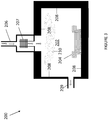
Figure 3 illustrates a preliminary contamination control process that includes introducing a first process gas into the interior chamber of the etching tool, according to an embodiment. -
Figure 4 illustrates a protective layer that forms along interior surfaces of the etching tool as a result of the first process gas, according to an embodiment. -
Figure 5 illustrates etching a semiconductor wafer with the protective layer covering the interior surfaces of the etching tool, according to an embodiment. -
Figure 6 illustrates an ashing step to remove a mask from the semiconductor wafer, according to an embodiment. -
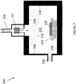
Figure 7 illustrates a preliminary contamination control process that includes introducing a first process gas into the etching tool, according to another embodiment. -
Figure 8 illustrates a protective layer that forms along interior surfaces of the etching tool as a result of the first process gas, according to another embodiment. - According to embodiments described herein, a process cycle for etching a type III-V semiconductor wafer is disclosed. The process cycle includes a preliminary step of conditioning the etch chamber prior to the etching process. This preliminary step of conditioning the etch chamber includes forming a polymer coating on the interior surfaces of the etch chamber. The polymer coating can be formed using an in-situ technique in which process gas, such as a CxHyClz containing gas mixture, is introduced into the etch chamber using the process gas intake mechanism of the etching tool. The process gas forms a protective polymer coating along the exposed surfaces of the interior chamber. After the protective polymer coating is formed, a wafer is inserted in the etch chamber and an etching process, such as plasma etching, is performed. Subsequently, an oxygen based ashing step can be performed to remove the polymer coating. During this ashing step, at least some of the resistive mask of the wafer can be removed. The same process cycle can be repeated multiple times for the etching of multiple semiconductor wafers.
- The above described process cycle advantageously produces a highly controlled and contaminant free environment for the etching process. Moreover, the etching environment is highly consistent as between each semiconductor wafer that is etched in different process cycles. In particular, the embodiments described herein substantially limit and control the amount of residual oxygen that is present in the interior chamber of the etching tool during the etch cycle. Oxygen is a known contaminant that dramatically impacts etch quality and leads to non-desirable etched surfaces including highly roughened surface and/or surface structures. The carbon protective layer substantially limits the number of contaminants such as oxygen in the etching tool by protecting the interior surfaces from being etched and by absorbing free radical state oxygen.
- Advantageously, because embodiments of the presently disclosed techniques reform a protective layer prior to each etching cycle, the conditions of the interior chamber are effectively identical for each etching cycle. Conventionally, protective layers for etch chambers are formed at the beginning of a production cycle. That is, the protective layer is not reformed prior to each subsequent wafer etch in the wafer lot. These methods require the protective layer to be very thick because it must survive multiple etching and ashing cycles. A notable drawback of this technique is that the protective layer gradually disintegrates over multiple etching cycles. Thus, the etch conditions for the etching of each wafer are not identical, as some contaminants tend to accumulate in the protective layer over multiple etch cycles. According to the present techniques, the protective layer can be much thinner, as it only needs to withstand a single etching cycle. Moreover, although the protective layer may partially or completely disintegrate during the ashing step, this does not detrimentally impact the subsequent etching cycle, as a new and substantially contaminant free protective layer is reformed prior to each wafer etch.
- Advantageously, the above described process cycle utilizes an in-situ technique to form the protective layer. Conventionally, protective layers for etch chambers are formed using an ex-situ technique whereby, before each wafer lot is processed, a dummy wafer is inserted into the etching tool and a portion of the dummy wafer is etched away, resulting in a residue that forms in the etching tool. One drawback of this technique is that it requires an additional process step of inserting and etching the dummy wafer before each lot is processed, and removing the protective layer after each lot is processed. These steps add significant delay and complication to the etching process. By contrast, the presently disclosed techniques utilize an in-situ technique, they can be seamlessly integrated into the etching process with minimal additional time and expense. Moreover, cleaning of the protective material from the etching tool after each lot is processed is not necessary, as the protective layer can be completely removed by the ashing cycle.
- Referring to
Fig. 1 , awafer lot 100 and a plan view of one of thesemiconductor wafers 102 in thewafer lot 100 are depicted. Thewafer lot 100 includes a plurality ofidentical semiconductor wafers 102. In the depicted embodiment, thewafer lot 100 includes fivesemiconductor wafers 102. More generally, thewafer lot 100 can include any number ofsemiconductor wafers 102 greater than two, e.g., 10, 20, 25, 50, etc. - In general, the
semiconductor wafers 102 can include any of a wide variety of semiconductor materials, such as silicon (Si), group IV compound semiconductor materials such as silicon carbide (SiC) or silicon germanium (SiGe), type III-V semiconductors including gallium nitride, gallium arsenide (GaAs), aluminium nitride (AlN), aluminium arsenide (AlAs), indium nitride (InN), indium arsenide (InAs), etc. According to an embodiment, each of thesemiconductor wafers 102 is a type III-V semiconductor wafer. Thesewafers 102 may be compound semiconductor wafers that include a silicon base wafer with a number of type III-V semiconductor layers epitaxially grown on the silicon base wafer. - Referring to
Fig. 2 , anetching tool 200 is depicted, according to an embodiment. Generally speaking, theetching tool 200 can be any commercially available semiconductor wafer processing tool that is designed to perform an etch process, such as plasma etching. Theetching tool 200 includes aninterior chamber 202, i.e., a three-dimensional space that is enclosed. Awafer chuck 204 is disposed within theinterior chamber 202. Thewafer chuck 204 is an apparatus that receives a single semiconductor wafer and securely retains the wafer in place, e.g., by a vacuum mechanism, while the wafer is being processed. Theetching tool 200 includes amechanism 206 for introducing process gas, into theinterior chamber 202. Theetching tool 200 may also include anRF coil 207 for generating a plasma from process gas. Theetching tool 200 may also include anRF coil 207 for generating a plasma from process gas and anexhaust mechanism 209 for removing process gasses from theinterior chamber 202. - Referring to
Fig. 3 , a preliminary contamination control process for coatinginterior surfaces 208 of theetching tool 200 is depicted, according to an embodiment. This preliminary contamination control process is performed prior to the etching of a semiconductor wafer. According to an embodiment, the preliminary contamination control process is performed without any semiconductor wafer being present in theinterior chamber 202. The preliminary contamination control process includes introducing afirst process gas 210 into theinterior chamber 202. Thefirst process gas 210 is introduced using a mechanism 206 (e.g., a chute) that is in open communication with theinterior chamber 202. Generally speaking, thefirst process gas 210 can include any gas that forms a substantially oxygen free polymer. Examples of these process gasses include carbon and hydrogen containing gasses or plasmas. More particularly, thefirst process gas 210 can include a CxHy containing gas mixture or a CxHyClz containing gas mixture. According to one embodiment, thefirst process gases 210 is C2H4 According to an embodiment, the first process gasfirst process gas 210 is energized into a plasma state, e.g., using theRF coil 207. - Referring to
Fig. 4 , as a result of thefirst process gas 210 being introduced into theinterior chamber 202 and being transformed into a plasma as described with reference toFig. 3 , aprotective layer 212 is formed along exposedinterior surfaces 208 of theinterior chamber 202. Generally speaking, the parameters of the preliminary contamination control process can be selected such that the fully formedprotective layer 212 is partially or completely removed after one etching and ashing sequence, such as the etching and ashing steps to be described in further detail below with reference toFigs. 5 and6 . The thickness of theprotective layer 212, which is dependent upon the parameters of the process described with reference toFig. 3 (e.g., time and temperature of exposure to the first process gas 210), can be selected to be relatively thin. For example, theprotective layer 212 can be formed to be about 1 nm (nanometer) - 1 µm (micron, and more particularly about 100nm - 500nm. These thicknesses provide adequate protection for at least one, and in some cases, only one, etching and ashing sequence. The material composition of theprotective layer 212 is correlated to the composition of thefirst process gas 210. Using the carbon and hydrogen containing gases described above as exemplaryfirst process gasses 210, these gasses form a carbon-based polymer, such as along theinterior surfaces 208 of theinterior chamber 202. Generally speaking, the carbon-based polymer can be any polymer containing carbon (C), hydrogen (H), and chlorine (CI). For example, the carbon-based polymer can be a carbon and hydrogen based polyethylene (C2H4) or variants thereof. These carbon-based polymers serve to protect theinterior surfaces 208 of theinterior chamber 202 while absorbing oxygen during an etching step. - The technique for forming the
protective layer 212 illustrated inFigs. 3 and4 is an in-situ process. As used herein, an in-situ process refers to a processing technique whereby the material that forms theprotective layer 212 is introduced into theinterior chamber 202 in the form of a process gas that is fed through theprocess gas mechanism 206 of theetching tool 200. That is, the material that ultimately forms theprotective layer 212 enters theinterior chamber 202 in a gaseous or plasma state, and eventually accumulates in a solid state along exposedinterior surfaces 208 of theinterior chamber 202. By way of comparison, an ex-situ technique refers to a technique whereby an extraneous object is used to introduce a foreign material into theinterior chamber 202. For example, an ex-situ technique encompasses a technique whereby a dummy wafer containing a foreign material is placed in theinterior chamber 202 and subsequently etched, resulting in a residue of the foreign material coating theinterior chamber 202. Thus, whereas an in-situ technique utilizes the inherent plasma generation functionality of theetching tool 200 to coat theinterior chamber 202, an ex-situ technique requires an extraneous article to coat theinterior chamber 202. - Referring to
Fig. 5 ., after forming theprotective layer 212, an etching step of the process cycle is performed. This process step includes inserting one of thesemiconductor wafers 102 of thewafer lot 100 into theinterior chamber 202 of theetching tool 200. The semiconductor wafer can be secured to thewafer chuck 204 in a commonly known manner. The semiconductor wafer can include apatterned mask 104 that covers an upper surface of thesemiconductor wafer 102 in certain locations and exposes the upper surface of thesemiconductor wafer 102 in the patterned region of themask 104. Themask 104 can be formed from any of a wide variety of conventionally known masking materials, including photoresist materials and oxides. After thesemiconductor wafer 102 is inserted into theinterior chamber 202, asecond process gas 214 is introduced into theinterior chamber 202 using the mechanism for introducing process gas. Generally speaking, thesecond process gas 214 can be any energized gas that is capable of reacting with the material of thesemiconductor wafer 102, selective to the material of themask 104, so as to remove material away from the unmasked portion of thesemiconductor wafer 102. Examples of these process gasses include fluorine and chlorine containing gasses, such as fluorine and chlorine. According to an embodiment, thesecond process gas 214 is in a plasma state. As a result of the etching step, arecess 106 is formed at the upper surface of thesemiconductor wafer 102. - Due to the presence of the
protective layer 212 in theinterior chamber 202 of theetching tool 200, none of theinterior surfaces 208 of the etch chamber react with thesecond process gas 214. Thus, the presence of contaminants in theinterior chamber 202 of theetching tool 200 in subsequent processing steps is minimized. - Referring to
Fig. 6 , after etching the semiconductor wafer, an ashing step of the process cycle can be performed. The ashing step includes introducing athird process gas 216 into theinterior chamber 202 using themechanism 106 for introducing process gas. In general, thethird process gas 216 can be any gas which, as a plasma, is capable of removing the material of themask 104, selective to the material of thesemiconductor wafer 102. For example, according to an embodiment,third process gas 216 is an oxygen (O2) based plasma. As a result of the ashing step, theprotective layer 212 is thinned, and contaminants from theprotective layer 212 are removed. In some cases, the ashing step may result in partial or complete removal of theprotective layer 212 from the exposedinterior surfaces 208 of the etch chamber. As a result, the presence of contaminants in theinterior chamber 202 of theetching tool 200 in subsequent processing steps is minimized. In addition, the ashing step may partially or completely remove themask 104 is removed from thesemiconductor wafer 102. Alternatively, thesemiconductor wafer 102 can be removed prior to the above described ashing step. - After performing the ashing step described with reference to
Fig. 6 , thesemiconductor wafer 102 is removed from theinterior chamber 202 of theetching tool 200. Subsequently, the process cycle described with reference toFigs. 3-6 can be repeated for some or all of thewafers 102 in thewafer lot 100. That is, the preliminary contamination control process described with reference toFigs. 3 and4 can be performed again without any wafer being present in theinterior chamber 202. Subsequently, an additional one of thesemiconductor wafers 102 in thewafer lot 100 can be inserted in theinterior chamber 202 and the etching and ashing steps described with reference toFigs. 5 and6 can be performed. -
Figs. 7 and8 depict an alternate embodiment of the preliminary contamination control process. Different to the technique described with reference toFigs. 3 and4 , the technique described with reference toFigs. 7 and8 is designed to withstand at least two etching cycles. - Referring to
Fig. 7 , afirst process gas 210 is introduced into theinterior chamber 202 in a similar manner as described with reference toFigs. 3 and4 . Thefirst process gas 210 can include carbon and hydrogen containing gasses such as a CxHy containing gas mixture or a CxHyClz containing gas mixture. Thefirst process gas 210 is introduced using amechanism 206 that is in open communication with theinterior chamber 202. - According to an embodiment, a
dummy wafer 108 is situated in thewafer chuck 204 during the introduction of thefirst process gas 210. Thedummy wafer 108 acts as a physical placeholder that covers thewafer chuck 204. As a result, thewafer chuck 204 is not exposed to thefirst process gas 210. Thedummy wafer 108 can be formed from different materials as thesemiconductor wafers 102 of thewafer lot 100. Thedummy wafer 108 can include any of a wide variety of materials, and is not necessarily semiconducting. - Referring to
Fig. 8 , after sufficient time and temperature of exposing thefirst process gas 210 to theinterior chamber 202, aprotective layer 212 is formed in theinterior chamber 202 of theetching tool 200. Different to the preliminary contamination control process described with reference toFigs. 3 and4 , in this embodiment, the parameters of the preliminary contamination control process are selected such that the fully formedprotective layer 212 is sufficiently thick to withstand more than one etching and ashing sequences, such as the etching and ashing steps described with reference toFigs. 5 and6 . For example, theprotective layer 212 can be formed to be about 500 nm - 2 µm thick, which is suitable to withstand two etching and ashing sequences. Moreover, the material composition of theprotective layer 212, which is correlated to the composition of thefirst process gas 210 can be selected to provide aprotective layer 212 that is able to withstand at least two of the etching and ashing sequences. In the embodiments in which thedummy wafer 108 is situated in thewafer chuck 204 during the exposure to thefirst process gas 210, theprotective layer 212 forms on thedummy wafer 108 and not the receptacle portion of thewafer chuck 204. Thus, as depicted inFig. 8 , when thedummy wafer 108 is removed from thewafer chuck 204, the receptacle portion of thewafer chuck 204 is devoid of theprotective layer 212. - The preliminary contamination control process described with reference to
Figs. 7 and8 allow for the preliminary contamination control process step to be omitted in at least some of the process cycles for eachwafer lot 100. That is, after performing the preliminary contamination control process described with reference toFigs. 7-8 , the process steps described with reference toFigs. 5 and6 can be performed on afirst semiconductor wafer 102 in thewafer lot 100 and can be repeated immediately thereafter on asecond semiconductor wafer 102 in thewafer lot 100. For example, according to an embodiment, the preliminary contamination control process described with reference toFigs. 7 and8 is performed once for each threesemiconductor wafers 102 that are etched. - The technique described with reference to
Figs. 7-8 offers certain advantages in that the cycle time per wafer can be reduced in comparison to the technique described with reference toFigs. 3-6 , as the preliminary contamination control process is not performed each cycle. On the other hand, the sufficiently higher thickness values of theprotective layer 212 that are required in the technique ofFigs. 7-8 so that theprotective layer 212 can withstand multiple etching and ashing sequences may require the use of thedummy wafer 108 to protect the receptacle portion of thewafer chuck 204. Without thedummy wafer 108, theprotective layer 212 that forms on the receptacle portion can interfere with the mechanical and thermal connection between thesemiconductor wafer 102 and thewafer chuck 204. By contrast, thedummy wafer 108 can be omitted in the technique described with reference toFigs. 3-6 because the thinnerprotective layer 212 of this embodiment is less likely to interfere with the mechanical and thermal connection between thesemiconductor wafer 102 and thewafer chuck 204. In other words, each technique offers different advantages and drawbacks, and selection of one technique over another is dependent on a variety of factors, such as composition of theprotective layer 212, number ofwafers 102 in thewafer lot 100, etc. - Spatially relative terms such as "under," "below," "lower," "over," "upper" and the like, are used for ease of description to explain the positioning of one element relative to a second element. These terms are intended to encompass different orientations of the device in addition to different orientations than those depicted in the figures. Further, terms such as "first," "second," and the like, are also used to describe various elements, regions, sections, etc. and are also not intended to be limiting. Like terms refer to like elements throughout the description.
- As used herein, the terms "having," "containing," "including," "comprising" and the like are open-ended terms that indicate the presence of stated elements or features, but do not preclude additional elements or features. The articles "a," "an" and "the" are intended to include the plural as well as the singular, unless the context clearly indicates otherwise.
- With the above range of variations and applications in mind, it should be understood that the present invention is not limited by the foregoing description, nor is it limited by the accompanying drawings. Instead, the present invention is limited only by the following claims and their legal equivalents.
Claims (15)
- A method of fabricating a type III-V semiconductor device, the method comprising:providing an etching tool that comprises an interior chamber;providing a plurality of type III-V semiconductor wafers;performing a process cycle for each one of the type III-V semiconductor wafers in the plurality, the process cycle comprising:performing a preliminary contamination control process;inserting one of the type III-V semiconductor wafers into the interior chamber;etching type III-V semiconductor material away from the type III-V semiconductor wafer that is present in the interior chamber; and removing the type III-V semiconductor wafer that is present in the interior chamber,wherein the preliminary contamination control process comprises forming a carbon containing protective material that covers exposed surfaces of the interior chamber.
- The method of claim 1, wherein the preliminary contamination control process comprises an in-situ process wherein a first process gas is introduced into the interior chamber, the first process gas forming the carbon containing protective material.
- The method of claim 1 or claim 2, wherein the preliminary contamination control process of the process cycle is performed without any wafer being present in the interior chamber.
- The method of any one of claims 1 to 3, wherein the process cycle further comprises:performing an oxygen based ashing step after the etching of the type III-V semiconductor material away from the type III-V semiconductor wafer that is present in the interior chamber,wherein the oxygen based ashing step at least partially removes the carbon containing protective material from the inner sidewalls of the interior chamber.
- The method of any one of claims 2 to 4, wherein the first process gas comprises at least one of: a CxHy containing gas mixture, preferably C2H4, and a CxHyClz containing gas mixture.
- A method of fabricating a type III-V semiconductor device, the method comprising:providing an etching tool that comprises an interior chamber;forming a carbon containing protective material that covers exposed surfaces of the interior chamber;inserting a first type III-V semiconductor wafer into the interior chamber with the protective material covering the exposed surfaces of the interior chamber;etching type III-V semiconductor material away from the first type III-V semiconductor wafer that is contained within the interior chamber while the protective material covers the exposed surfaces of the interior chamber;performing a first oxygen based ashing step to at least partially remove the protective material from the exposed surfaces of the interior chamber;wherein the preliminary contamination control process comprises an in-situ process wherein a first process gas is introduced into the interior chamber, the first process gas forming the carbon containing protective material.
- The method of claim 6, wherein the first process gas comprises at least one of: a CxHy containing gas mixture, preferably C2H4, and a CxHyClz containing gas mixture.
- The method of claim 6 or claim 7, wherein the forming of the carbon containing protective material is performed without any wafer being present in the interior chamber.
- The method of any one of claim 6 to 8, wherein performing the first oxygen based ashing step at least partially removes the protective coating from the interior walls of the interior chamber.
- The method of any one of claims 7 to 9, further comprising, after performing the first oxygen based ashing step:removing the first type III-V semiconductor wafer from the interior chamber;inserting a second type III-V semiconductor wafer into the interior chamber with the protective material covering the exposed surfaces of the interior chamber;etching type III-V semiconductor material away from the second type III-V semiconductor wafer that is contained within the interior chamber while the protective material covers the exposed surfaces of the interior chamber; andperforming a second oxygen based ashing step to remove the protective material from the exposed surfaces of the interior chamber.
- The method of claim 10, wherein the carbon containing protective material is formed before inserting the first type III-V semiconductor wafer into the interior chamber and is not formed after removing the first type III-V semiconductor wafer from the interior chamber, and wherein the carbon containing protective material is formed to be sufficiently thick such that the protective coating completely covers the exposed surfaces of the interior chamber after both the first oxygen based ashing step and the second oxygen based ashing step.
- The method of claim 11, wherein the etching tool comprises a wafer chuck, and wherein the carbon containing protective material is formed with a dummy wafer being present in the wafer chuck.
- A method of conditioning an etch chamber for each processing cycle during the processing of multiple III-V semiconductor wafers, the method comprising:depositing a polymer coating on an inner surface of the etch chamber via a carbon-containing plasma present in the etch chamber without a III-V semiconductor wafer in the etch chamber;removing the polymer coating from the inner surface of the etch chamber after a single III-V semiconductor wafer is processed in the etch chamber; andrepeating the polymer coating deposition and removal processes for each subsequent III-V semiconductor wafer to be processed in the etch chamber.
- The method of claim 13, wherein removing the polymer coating from the inner surface of the etch chamber comprises performing an oxygen based ashing step after the single III-V semiconductor wafer is processed in the etch chamber.
- The method of claim 13 or claim 14, wherein the carbon-containing plasma comprises at least one of: a CxHy containing gas mixture, preferably, C2H4., and a CxHyClz containing gas mixture.
Applications Claiming Priority (1)
| Application Number | Priority Date | Filing Date | Title |
|---|---|---|---|
| US15/638,558 US10128133B1 (en) | 2017-06-30 | 2017-06-30 | Method of conditioning an etch chamber for contaminant free etching of a semiconductor device |
Publications (2)
| Publication Number | Publication Date |
|---|---|
| EP3422391A1 true EP3422391A1 (en) | 2019-01-02 |
| EP3422391B1 EP3422391B1 (en) | 2024-04-03 |
Family
ID=62791523
Family Applications (1)
| Application Number | Title | Priority Date | Filing Date |
|---|---|---|---|
| EP18179198.9A Active EP3422391B1 (en) | 2017-06-30 | 2018-06-22 | Method of conditioning an etch chamber for contaminant free etching of a semiconductor device |
Country Status (2)
| Country | Link |
|---|---|
| US (1) | US10128133B1 (en) |
| EP (1) | EP3422391B1 (en) |
Families Citing this family (1)
| Publication number | Priority date | Publication date | Assignee | Title |
|---|---|---|---|---|
| US20240266149A1 (en) * | 2023-02-03 | 2024-08-08 | Tokyo Electron Limited | Methods for Semiconductor Process Chamber |
Family Cites Families (2)
| Publication number | Priority date | Publication date | Assignee | Title |
|---|---|---|---|---|
| US6350697B1 (en) | 1999-12-22 | 2002-02-26 | Lam Research Corporation | Method of cleaning and conditioning plasma reaction chamber |
| US7094670B2 (en) * | 2000-08-11 | 2006-08-22 | Applied Materials, Inc. | Plasma immersion ion implantation process |
-
2017
- 2017-06-30 US US15/638,558 patent/US10128133B1/en active Active
-
2018
- 2018-06-22 EP EP18179198.9A patent/EP3422391B1/en active Active
Non-Patent Citations (1)
| Title |
|---|
| T. R. HAYES: "Reactive ion etching of InP using CH4/H2 mixtures: Mechanisms of etching and anisotropy", JOURNAL OF VACUUM SCIENCE & TECHNOLOGY B: MICROELECTRONICSPROCESSING AND PHENOMENA., vol. 7, no. 5, 1 September 1989 (1989-09-01), US, pages 1130 - 1140, XP055508549, ISSN: 0734-211X, DOI: 10.1116/1.584564 * |
Also Published As
| Publication number | Publication date |
|---|---|
| US10128133B1 (en) | 2018-11-13 |
| EP3422391B1 (en) | 2024-04-03 |
Similar Documents
| Publication | Publication Date | Title |
|---|---|---|
| CN103094335B (en) | High electron mobility transistor and forming method thereof | |
| TWI500149B (en) | GaN high voltage heterojunction field effect transistor with passivation gate dielectric multilayer structure | |
| EP2772940B1 (en) | Heterostructure Power Transistor with AlSiN Passivation Layer | |
| US8624296B1 (en) | High electron mobility transistor including an embedded flourine region | |
| US20240371941A1 (en) | Fully strained channel | |
| US11164767B2 (en) | Integrated system for semiconductor process | |
| CN102292800A (en) | Dual high-k oxide with SiGe channel | |
| CN102290374A (en) | Method for manufacturing integrated circuit device | |
| CN108352324B (en) | Non-etching gas cooled epitaxial stack for group IIIA-N devices | |
| TW202020965A (en) | Method for protecting nitride layer during formation of silicon germanium nanowire in microelectronic work piece | |
| US20230223273A1 (en) | Plasma-based method for delayering of circuits | |
| CN103000516B (en) | The method forming semiconductor structure | |
| CN103050511B (en) | Semiconductor structure and the method forming semiconductor structure | |
| US10128133B1 (en) | Method of conditioning an etch chamber for contaminant free etching of a semiconductor device | |
| US20240105450A1 (en) | Group iii-v semiconductor device and method of fabrication of same including in-situ surface passivation | |
| WO2022205469A1 (en) | Iii nitride semiconductor wafers | |
| US9698238B2 (en) | Method of forming ultra-thin nanowires | |
| US10121698B2 (en) | Method of manufacturing a semiconductor device | |
| US9922936B1 (en) | Semiconductor lithography alignment feature with epitaxy blocker | |
| US10403496B2 (en) | Compound semiconductor substrate and method of forming a compound semiconductor substrate | |
| US20080199993A1 (en) | Protective layer in device fabrication | |
| CN109585267B (en) | Silicon nitride film formation method | |
| US10872760B2 (en) | Cluster tool and manufacuturing method of semiconductor structure using the same | |
| EP3764401B1 (en) | Insulating structure of high electron mobility transistor and manufacturing method thereof | |
| JP2025515386A (en) | Method for forming a dielectric material-based layer on an etched III-V material-based layer - Patents.com |
Legal Events
| Date | Code | Title | Description |
|---|---|---|---|
| PUAI | Public reference made under article 153(3) epc to a published international application that has entered the european phase |
Free format text: ORIGINAL CODE: 0009012 |
|
| STAA | Information on the status of an ep patent application or granted ep patent |
Free format text: STATUS: THE APPLICATION HAS BEEN PUBLISHED |
|
| AK | Designated contracting states |
Kind code of ref document: A1 Designated state(s): AL AT BE BG CH CY CZ DE DK EE ES FI FR GB GR HR HU IE IS IT LI LT LU LV MC MK MT NL NO PL PT RO RS SE SI SK SM TR |
|
| AX | Request for extension of the european patent |
Extension state: BA ME |
|
| RIN1 | Information on inventor provided before grant (corrected) |
Inventor name: OSTERMAIER, CLEMENS Inventor name: HAGHOFER, ANDREAS |
|
| STAA | Information on the status of an ep patent application or granted ep patent |
Free format text: STATUS: REQUEST FOR EXAMINATION WAS MADE |
|
| 17P | Request for examination filed |
Effective date: 20190702 |
|
| RBV | Designated contracting states (corrected) |
Designated state(s): AL AT BE BG CH CY CZ DE DK EE ES FI FR GB GR HR HU IE IS IT LI LT LU LV MC MK MT NL NO PL PT RO RS SE SI SK SM TR |
|
| STAA | Information on the status of an ep patent application or granted ep patent |
Free format text: STATUS: EXAMINATION IS IN PROGRESS |
|
| 17Q | First examination report despatched |
Effective date: 20210908 |
|
| GRAP | Despatch of communication of intention to grant a patent |
Free format text: ORIGINAL CODE: EPIDOSNIGR1 |
|
| STAA | Information on the status of an ep patent application or granted ep patent |
Free format text: STATUS: GRANT OF PATENT IS INTENDED |
|
| INTG | Intention to grant announced |
Effective date: 20231024 |
|
| GRAS | Grant fee paid |
Free format text: ORIGINAL CODE: EPIDOSNIGR3 |
|
| GRAA | (expected) grant |
Free format text: ORIGINAL CODE: 0009210 |
|
| STAA | Information on the status of an ep patent application or granted ep patent |
Free format text: STATUS: THE PATENT HAS BEEN GRANTED |
|
| P01 | Opt-out of the competence of the unified patent court (upc) registered |
Effective date: 20240130 |
|
| AK | Designated contracting states |
Kind code of ref document: B1 Designated state(s): AL AT BE BG CH CY CZ DE DK EE ES FI FR GB GR HR HU IE IS IT LI LT LU LV MC MK MT NL NO PL PT RO RS SE SI SK SM TR |
|
| REG | Reference to a national code |
Ref country code: GB Ref legal event code: FG4D |
|
| REG | Reference to a national code |
Ref country code: CH Ref legal event code: EP |
|
| REG | Reference to a national code |
Ref country code: IE Ref legal event code: FG4D |
|
| REG | Reference to a national code |
Ref country code: DE Ref legal event code: R096 Ref document number: 602018067405 Country of ref document: DE |
|
| REG | Reference to a national code |
Ref country code: LT Ref legal event code: MG9D |
|
| REG | Reference to a national code |
Ref country code: NL Ref legal event code: MP Effective date: 20240403 |
|
| REG | Reference to a national code |
Ref country code: AT Ref legal event code: MK05 Ref document number: 1673341 Country of ref document: AT Kind code of ref document: T Effective date: 20240403 |
|
| PG25 | Lapsed in a contracting state [announced via postgrant information from national office to epo] |
Ref country code: NL Free format text: LAPSE BECAUSE OF FAILURE TO SUBMIT A TRANSLATION OF THE DESCRIPTION OR TO PAY THE FEE WITHIN THE PRESCRIBED TIME-LIMIT Effective date: 20240403 |
|
| PG25 | Lapsed in a contracting state [announced via postgrant information from national office to epo] |
Ref country code: NL Free format text: LAPSE BECAUSE OF FAILURE TO SUBMIT A TRANSLATION OF THE DESCRIPTION OR TO PAY THE FEE WITHIN THE PRESCRIBED TIME-LIMIT Effective date: 20240403 |
|
| PG25 | Lapsed in a contracting state [announced via postgrant information from national office to epo] |
Ref country code: IS Free format text: LAPSE BECAUSE OF FAILURE TO SUBMIT A TRANSLATION OF THE DESCRIPTION OR TO PAY THE FEE WITHIN THE PRESCRIBED TIME-LIMIT Effective date: 20240803 |
|
| PG25 | Lapsed in a contracting state [announced via postgrant information from national office to epo] |
Ref country code: BG Free format text: LAPSE BECAUSE OF FAILURE TO SUBMIT A TRANSLATION OF THE DESCRIPTION OR TO PAY THE FEE WITHIN THE PRESCRIBED TIME-LIMIT Effective date: 20240403 |
|
| PG25 | Lapsed in a contracting state [announced via postgrant information from national office to epo] |
Ref country code: HR Free format text: LAPSE BECAUSE OF FAILURE TO SUBMIT A TRANSLATION OF THE DESCRIPTION OR TO PAY THE FEE WITHIN THE PRESCRIBED TIME-LIMIT Effective date: 20240403 Ref country code: FI Free format text: LAPSE BECAUSE OF FAILURE TO SUBMIT A TRANSLATION OF THE DESCRIPTION OR TO PAY THE FEE WITHIN THE PRESCRIBED TIME-LIMIT Effective date: 20240403 |
|
| PG25 | Lapsed in a contracting state [announced via postgrant information from national office to epo] |
Ref country code: GR Free format text: LAPSE BECAUSE OF FAILURE TO SUBMIT A TRANSLATION OF THE DESCRIPTION OR TO PAY THE FEE WITHIN THE PRESCRIBED TIME-LIMIT Effective date: 20240704 |
|
| PG25 | Lapsed in a contracting state [announced via postgrant information from national office to epo] |
Ref country code: PT Free format text: LAPSE BECAUSE OF FAILURE TO SUBMIT A TRANSLATION OF THE DESCRIPTION OR TO PAY THE FEE WITHIN THE PRESCRIBED TIME-LIMIT Effective date: 20240805 |
|
| PG25 | Lapsed in a contracting state [announced via postgrant information from national office to epo] |
Ref country code: ES Free format text: LAPSE BECAUSE OF FAILURE TO SUBMIT A TRANSLATION OF THE DESCRIPTION OR TO PAY THE FEE WITHIN THE PRESCRIBED TIME-LIMIT Effective date: 20240403 |
|
| PG25 | Lapsed in a contracting state [announced via postgrant information from national office to epo] |
Ref country code: CZ Free format text: LAPSE BECAUSE OF FAILURE TO SUBMIT A TRANSLATION OF THE DESCRIPTION OR TO PAY THE FEE WITHIN THE PRESCRIBED TIME-LIMIT Effective date: 20240403 |
|
| PG25 | Lapsed in a contracting state [announced via postgrant information from national office to epo] |
Ref country code: AT Free format text: LAPSE BECAUSE OF FAILURE TO SUBMIT A TRANSLATION OF THE DESCRIPTION OR TO PAY THE FEE WITHIN THE PRESCRIBED TIME-LIMIT Effective date: 20240403 |
|
| PG25 | Lapsed in a contracting state [announced via postgrant information from national office to epo] |
Ref country code: PL Free format text: LAPSE BECAUSE OF FAILURE TO SUBMIT A TRANSLATION OF THE DESCRIPTION OR TO PAY THE FEE WITHIN THE PRESCRIBED TIME-LIMIT Effective date: 20240403 |
|
| PG25 | Lapsed in a contracting state [announced via postgrant information from national office to epo] |
Ref country code: LV Free format text: LAPSE BECAUSE OF FAILURE TO SUBMIT A TRANSLATION OF THE DESCRIPTION OR TO PAY THE FEE WITHIN THE PRESCRIBED TIME-LIMIT Effective date: 20240403 |
|
| PG25 | Lapsed in a contracting state [announced via postgrant information from national office to epo] |
Ref country code: PT Free format text: LAPSE BECAUSE OF FAILURE TO SUBMIT A TRANSLATION OF THE DESCRIPTION OR TO PAY THE FEE WITHIN THE PRESCRIBED TIME-LIMIT Effective date: 20240805 Ref country code: PL Free format text: LAPSE BECAUSE OF FAILURE TO SUBMIT A TRANSLATION OF THE DESCRIPTION OR TO PAY THE FEE WITHIN THE PRESCRIBED TIME-LIMIT Effective date: 20240403 Ref country code: NO Free format text: LAPSE BECAUSE OF FAILURE TO SUBMIT A TRANSLATION OF THE DESCRIPTION OR TO PAY THE FEE WITHIN THE PRESCRIBED TIME-LIMIT Effective date: 20240703 Ref country code: LV Free format text: LAPSE BECAUSE OF FAILURE TO SUBMIT A TRANSLATION OF THE DESCRIPTION OR TO PAY THE FEE WITHIN THE PRESCRIBED TIME-LIMIT Effective date: 20240403 Ref country code: IS Free format text: LAPSE BECAUSE OF FAILURE TO SUBMIT A TRANSLATION OF THE DESCRIPTION OR TO PAY THE FEE WITHIN THE PRESCRIBED TIME-LIMIT Effective date: 20240803 Ref country code: HR Free format text: LAPSE BECAUSE OF FAILURE TO SUBMIT A TRANSLATION OF THE DESCRIPTION OR TO PAY THE FEE WITHIN THE PRESCRIBED TIME-LIMIT Effective date: 20240403 Ref country code: GR Free format text: LAPSE BECAUSE OF FAILURE TO SUBMIT A TRANSLATION OF THE DESCRIPTION OR TO PAY THE FEE WITHIN THE PRESCRIBED TIME-LIMIT Effective date: 20240704 Ref country code: FI Free format text: LAPSE BECAUSE OF FAILURE TO SUBMIT A TRANSLATION OF THE DESCRIPTION OR TO PAY THE FEE WITHIN THE PRESCRIBED TIME-LIMIT Effective date: 20240403 Ref country code: ES Free format text: LAPSE BECAUSE OF FAILURE TO SUBMIT A TRANSLATION OF THE DESCRIPTION OR TO PAY THE FEE WITHIN THE PRESCRIBED TIME-LIMIT Effective date: 20240403 Ref country code: CZ Free format text: LAPSE BECAUSE OF FAILURE TO SUBMIT A TRANSLATION OF THE DESCRIPTION OR TO PAY THE FEE WITHIN THE PRESCRIBED TIME-LIMIT Effective date: 20240403 Ref country code: BG Free format text: LAPSE BECAUSE OF FAILURE TO SUBMIT A TRANSLATION OF THE DESCRIPTION OR TO PAY THE FEE WITHIN THE PRESCRIBED TIME-LIMIT Effective date: 20240403 Ref country code: AT Free format text: LAPSE BECAUSE OF FAILURE TO SUBMIT A TRANSLATION OF THE DESCRIPTION OR TO PAY THE FEE WITHIN THE PRESCRIBED TIME-LIMIT Effective date: 20240403 Ref country code: RS Free format text: LAPSE BECAUSE OF FAILURE TO SUBMIT A TRANSLATION OF THE DESCRIPTION OR TO PAY THE FEE WITHIN THE PRESCRIBED TIME-LIMIT Effective date: 20240703 |
|
| REG | Reference to a national code |
Ref country code: DE Ref legal event code: R097 Ref document number: 602018067405 Country of ref document: DE |
|
| PG25 | Lapsed in a contracting state [announced via postgrant information from national office to epo] |
Ref country code: DK Free format text: LAPSE BECAUSE OF FAILURE TO SUBMIT A TRANSLATION OF THE DESCRIPTION OR TO PAY THE FEE WITHIN THE PRESCRIBED TIME-LIMIT Effective date: 20240403 |
|
| PG25 | Lapsed in a contracting state [announced via postgrant information from national office to epo] |
Ref country code: EE Free format text: LAPSE BECAUSE OF FAILURE TO SUBMIT A TRANSLATION OF THE DESCRIPTION OR TO PAY THE FEE WITHIN THE PRESCRIBED TIME-LIMIT Effective date: 20240403 |
|
| PG25 | Lapsed in a contracting state [announced via postgrant information from national office to epo] |
Ref country code: RO Free format text: LAPSE BECAUSE OF FAILURE TO SUBMIT A TRANSLATION OF THE DESCRIPTION OR TO PAY THE FEE WITHIN THE PRESCRIBED TIME-LIMIT Effective date: 20240403 Ref country code: SK Free format text: LAPSE BECAUSE OF FAILURE TO SUBMIT A TRANSLATION OF THE DESCRIPTION OR TO PAY THE FEE WITHIN THE PRESCRIBED TIME-LIMIT Effective date: 20240403 |
|
| PG25 | Lapsed in a contracting state [announced via postgrant information from national office to epo] |
Ref country code: SM Free format text: LAPSE BECAUSE OF FAILURE TO SUBMIT A TRANSLATION OF THE DESCRIPTION OR TO PAY THE FEE WITHIN THE PRESCRIBED TIME-LIMIT Effective date: 20240403 |
|
| PG25 | Lapsed in a contracting state [announced via postgrant information from national office to epo] |
Ref country code: SM Free format text: LAPSE BECAUSE OF FAILURE TO SUBMIT A TRANSLATION OF THE DESCRIPTION OR TO PAY THE FEE WITHIN THE PRESCRIBED TIME-LIMIT Effective date: 20240403 Ref country code: SK Free format text: LAPSE BECAUSE OF FAILURE TO SUBMIT A TRANSLATION OF THE DESCRIPTION OR TO PAY THE FEE WITHIN THE PRESCRIBED TIME-LIMIT Effective date: 20240403 Ref country code: RO Free format text: LAPSE BECAUSE OF FAILURE TO SUBMIT A TRANSLATION OF THE DESCRIPTION OR TO PAY THE FEE WITHIN THE PRESCRIBED TIME-LIMIT Effective date: 20240403 Ref country code: EE Free format text: LAPSE BECAUSE OF FAILURE TO SUBMIT A TRANSLATION OF THE DESCRIPTION OR TO PAY THE FEE WITHIN THE PRESCRIBED TIME-LIMIT Effective date: 20240403 Ref country code: DK Free format text: LAPSE BECAUSE OF FAILURE TO SUBMIT A TRANSLATION OF THE DESCRIPTION OR TO PAY THE FEE WITHIN THE PRESCRIBED TIME-LIMIT Effective date: 20240403 Ref country code: MC Free format text: LAPSE BECAUSE OF FAILURE TO SUBMIT A TRANSLATION OF THE DESCRIPTION OR TO PAY THE FEE WITHIN THE PRESCRIBED TIME-LIMIT Effective date: 20240403 |
|
| REG | Reference to a national code |
Ref country code: CH Ref legal event code: PL |
|
| PLBE | No opposition filed within time limit |
Free format text: ORIGINAL CODE: 0009261 |
|
| STAA | Information on the status of an ep patent application or granted ep patent |
Free format text: STATUS: NO OPPOSITION FILED WITHIN TIME LIMIT |
|
| PG25 | Lapsed in a contracting state [announced via postgrant information from national office to epo] |
Ref country code: LU Free format text: LAPSE BECAUSE OF NON-PAYMENT OF DUE FEES Effective date: 20240622 |
|
| 26N | No opposition filed |
Effective date: 20250106 |
|
| GBPC | Gb: european patent ceased through non-payment of renewal fee |
Effective date: 20240703 |
|
| PG25 | Lapsed in a contracting state [announced via postgrant information from national office to epo] |
Ref country code: IE Free format text: LAPSE BECAUSE OF NON-PAYMENT OF DUE FEES Effective date: 20240622 |
|
| PG25 | Lapsed in a contracting state [announced via postgrant information from national office to epo] |
Ref country code: SI Free format text: LAPSE BECAUSE OF FAILURE TO SUBMIT A TRANSLATION OF THE DESCRIPTION OR TO PAY THE FEE WITHIN THE PRESCRIBED TIME-LIMIT Effective date: 20240403 Ref country code: CH Free format text: LAPSE BECAUSE OF NON-PAYMENT OF DUE FEES Effective date: 20240630 Ref country code: BE Free format text: LAPSE BECAUSE OF NON-PAYMENT OF DUE FEES Effective date: 20240630 |
|
| PG25 | Lapsed in a contracting state [announced via postgrant information from national office to epo] |
Ref country code: FR Free format text: LAPSE BECAUSE OF NON-PAYMENT OF DUE FEES Effective date: 20240630 |
|
| PG25 | Lapsed in a contracting state [announced via postgrant information from national office to epo] |
Ref country code: GB Free format text: LAPSE BECAUSE OF NON-PAYMENT OF DUE FEES Effective date: 20240703 |
|
| REG | Reference to a national code |
Ref country code: BE Ref legal event code: MM Effective date: 20240630 |
|
| PG25 | Lapsed in a contracting state [announced via postgrant information from national office to epo] |
Ref country code: SE Free format text: LAPSE BECAUSE OF FAILURE TO SUBMIT A TRANSLATION OF THE DESCRIPTION OR TO PAY THE FEE WITHIN THE PRESCRIBED TIME-LIMIT Effective date: 20240403 |
|
| PGFP | Annual fee paid to national office [announced via postgrant information from national office to epo] |
Ref country code: DE Payment date: 20250822 Year of fee payment: 8 |
|
| PG25 | Lapsed in a contracting state [announced via postgrant information from national office to epo] |
Ref country code: CY Free format text: LAPSE BECAUSE OF FAILURE TO SUBMIT A TRANSLATION OF THE DESCRIPTION OR TO PAY THE FEE WITHIN THE PRESCRIBED TIME-LIMIT; INVALID AB INITIO Effective date: 20180622 |
|
| REG | Reference to a national code |
Ref country code: DE Ref legal event code: R079 Ref document number: 602018067405 Country of ref document: DE Free format text: PREVIOUS MAIN CLASS: H01L0021306000 Ipc: H10P0050000000 |
|
| PG25 | Lapsed in a contracting state [announced via postgrant information from national office to epo] |
Ref country code: IT Free format text: LAPSE BECAUSE OF FAILURE TO SUBMIT A TRANSLATION OF THE DESCRIPTION OR TO PAY THE FEE WITHIN THE PRESCRIBED TIME-LIMIT Effective date: 20240403 |
|
| PG25 | Lapsed in a contracting state [announced via postgrant information from national office to epo] |
Ref country code: HU Free format text: LAPSE BECAUSE OF FAILURE TO SUBMIT A TRANSLATION OF THE DESCRIPTION OR TO PAY THE FEE WITHIN THE PRESCRIBED TIME-LIMIT; INVALID AB INITIO Effective date: 20180622 |
|
| PG25 | Lapsed in a contracting state [announced via postgrant information from national office to epo] |
Ref country code: TR Free format text: LAPSE BECAUSE OF FAILURE TO SUBMIT A TRANSLATION OF THE DESCRIPTION OR TO PAY THE FEE WITHIN THE PRESCRIBED TIME-LIMIT Effective date: 20240403 |
|
| PG25 | Lapsed in a contracting state [announced via postgrant information from national office to epo] |
Ref country code: LT Free format text: LAPSE BECAUSE OF FAILURE TO SUBMIT A TRANSLATION OF THE DESCRIPTION OR TO PAY THE FEE WITHIN THE PRESCRIBED TIME-LIMIT Effective date: 20240403 |