EP3422242A1 - Performing authenticated writes across aggregate storage volumes - Google Patents
Performing authenticated writes across aggregate storage volumes Download PDFInfo
- Publication number
- EP3422242A1 EP3422242A1 EP18174968.0A EP18174968A EP3422242A1 EP 3422242 A1 EP3422242 A1 EP 3422242A1 EP 18174968 A EP18174968 A EP 18174968A EP 3422242 A1 EP3422242 A1 EP 3422242A1
- Authority
- EP
- European Patent Office
- Prior art keywords
- storage array
- hash table
- aggregate
- aggregate storage
- data payload
- Prior art date
- Legal status (The legal status is an assumption and is not a legal conclusion. Google has not performed a legal analysis and makes no representation as to the accuracy of the status listed.)
- Granted
Links
Images
Classifications
-
- G—PHYSICS
- G06—COMPUTING OR CALCULATING; COUNTING
- G06F—ELECTRIC DIGITAL DATA PROCESSING
- G06F21/00—Security arrangements for protecting computers, components thereof, programs or data against unauthorised activity
- G06F21/60—Protecting data
- G06F21/64—Protecting data integrity, e.g. using checksums, certificates or signatures
- G06F21/645—Protecting data integrity, e.g. using checksums, certificates or signatures using a third party
-
- G—PHYSICS
- G06—COMPUTING OR CALCULATING; COUNTING
- G06F—ELECTRIC DIGITAL DATA PROCESSING
- G06F16/00—Information retrieval; Database structures therefor; File system structures therefor
- G06F16/10—File systems; File servers
- G06F16/18—File system types
- G06F16/182—Distributed file systems
- G06F16/184—Distributed file systems implemented as replicated file system
- G06F16/1844—Management specifically adapted to replicated file systems
-
- G—PHYSICS
- G06—COMPUTING OR CALCULATING; COUNTING
- G06F—ELECTRIC DIGITAL DATA PROCESSING
- G06F11/00—Error detection; Error correction; Monitoring
- G06F11/07—Responding to the occurrence of a fault, e.g. fault tolerance
- G06F11/16—Error detection or correction of the data by redundancy in hardware
- G06F11/1658—Data re-synchronization of a redundant component, or initial sync of replacement, additional or spare unit
- G06F11/1662—Data re-synchronization of a redundant component, or initial sync of replacement, additional or spare unit the resynchronized component or unit being a persistent storage device
-
- G—PHYSICS
- G06—COMPUTING OR CALCULATING; COUNTING
- G06F—ELECTRIC DIGITAL DATA PROCESSING
- G06F12/00—Accessing, addressing or allocating within memory systems or architectures
- G06F12/02—Addressing or allocation; Relocation
- G06F12/0223—User address space allocation, e.g. contiguous or non contiguous base addressing
- G06F12/023—Free address space management
-
- G—PHYSICS
- G06—COMPUTING OR CALCULATING; COUNTING
- G06F—ELECTRIC DIGITAL DATA PROCESSING
- G06F12/00—Accessing, addressing or allocating within memory systems or architectures
- G06F12/02—Addressing or allocation; Relocation
- G06F12/06—Addressing a physical block of locations, e.g. base addressing, module addressing, memory dedication
- G06F12/0646—Configuration or reconfiguration
-
- H—ELECTRICITY
- H04—ELECTRIC COMMUNICATION TECHNIQUE
- H04L—TRANSMISSION OF DIGITAL INFORMATION, e.g. TELEGRAPHIC COMMUNICATION
- H04L67/00—Network arrangements or protocols for supporting network services or applications
- H04L67/01—Protocols
- H04L67/10—Protocols in which an application is distributed across nodes in the network
- H04L67/1097—Protocols in which an application is distributed across nodes in the network for distributed storage of data in networks, e.g. transport arrangements for network file system [NFS], storage area networks [SAN] or network attached storage [NAS]
Definitions
- Storage of public and private cloud data may involve the use of authenticated writes to a storage platform.
- authentication may be achieved via a bidirectional encrypted session between two verified endpoints (e.g., a cloud service provider and the storage platform).
- two verified endpoints e.g., a cloud service provider and the storage platform.
- Such an approach may be relatively complex, inefficient and/or costly.
- the aggregate storage array 10 includes a plurality of storage devices 12.
- the aggregate storage array 10 is an all-flash array (AFA), a redundant array of independent disks (RAID), etc.
- each storage device (“drive") 12 is a solid state drive (SSD).
- the aggregate storage array 10 may be used to store data payloads such as, for example, financial data (e.g., digitized loan documents), boot images (e.g., for a tenant of a cloud service provider), and so forth.
- the aggregate storage array 10 may replicate data and/or correct errors on a storage block basis, wherein the block size may vary depending on the circumstances (e.g., 256 Kilobytes (KB), 512 KB, 4 Megabytes (MB)).
- writes to the aggregate storage array 10 may be authenticated (e.g., to prevent tampering or other unauthorized modifications of the data payloads) in a manner that does not involve a bidirectional encrypted session between each storage device 12 and another verified endpoint (e.g., the entity/component attempting the write operation). More particularly, the data payloads may be partitioned into storage blocks (e.g., pages) that are compatible with the data replication policy and error correction policy (e.g., error correction code/ECC) of the aggregate storage array 10. Additionally, a hash table may be generated to specify how to index into and individually authenticate the storage blocks on a per block basis, wherein the aggregate storage array 10 authenticates a digital signature applied to the hash table.
- storage blocks e.g., pages
- error correction policy e.g., error correction code/ECC
- the hash table is authenticated on the per block basis by each storage device 12 (e.g., at the drive level) of the aggregate storage array 10. Accordingly, the hash table may be used to narrow down the data authentication granularity to a single block within the plurality of blocks. Such an approach may enable authentication of the entire data payload to be avoided.
- the illustrated aggregate storage array 10 therefore provides a relatively simple, efficient and low cost solution to conducting authenticated writes.
- the array 10 may include one or more network interface cards (NICs), switch nodes and/or processors (e.g., compute nodes in a chassis "hot zone") that facilitate modular connectivity to the storage devices 12.
- Each storage device 12 may be, for example, relatively thin and long (e.g., nineteen inches) ruler shaped SSD (RSSD).
- RSSD ruler shaped SSD
- the aggregate storage array 10 might include thirty-two RSSDs positioned at the front of the aggregate storage array 10 and coupled to the chassis hot zone at the rear of the aggregate storage array 10.
- the SSDs may therefore be aggregated and presented to a host as a single device to achieve greater storage density.
- the aggregate storage array 10 may be used for a NAND flash memory, three-dimensional (3D) NAND memory array devices, or other memory devices.
- Non-volatile memory is a storage medium that does not require power to maintain the state of data stored by the medium.
- the storage devices 12 are block addressable memory devices, such as those based on NAND or NOR technologies.
- a memory device may also include future generation nonvolatile devices, such as a three dimensional (3D) crosspoint memory device, or other byte addressable write-in-place nonvolatile memory devices.
- the memory device may be or may include memory devices that use silicon-oxide-nitride-oxide-silicon (SONOS) memory, electrically erasable programmable read-only memory (EEPROM), chalcogenide glass, multi-threshold level NAND flash memory, NOR flash memory, single or multi-level Phase Change Memory (PCM), a resistive memory, nanowire memory, ferroelectric transistor random access memory (FeTRAM), anti-ferroelectric memory, magnetoresistive random access memory (MRAM) memory that incorporates memristor technology, resistive memory including the metal oxide base, the oxygen vacancy base and the conductive bridge Random Access Memory (CB-RAM), or spin transfer torque (STT)-MRAM, a spintronic magnetic junction memory based device, a magnetic tunneling junction (MTJ) based device, a DW (Domain Wall) and SOT (Spin Orbit Transfer) based device, a thiristor based memory device, or a combination of any of the above, or other memory
- the memory device may refer to the die itself and/or to a packaged memory product.
- 3D crosspoint memory may comprise a transistor-less stackable cross point architecture in which memory cells sit at the intersection of words lines and bit lines and are individually addressable and in which bit storage is based on a change in bulk resistance.
- a memory module with non-volatile memory may comply with one or more standards promulgated by the Joint Electron Device Engineering Council (JEDEC), such as JESD218, JESD219, JESD220-1, JESD223B, JESD223-1, or other suitable standard (the JEDEC standards cited herein are available at jedec.org).
- JEDEC Joint Electron Device Engineering Council
- FIG. 2 shows an authenticated write architecture 14 in which a binary update image 16 (e.g., data payload) is sent to an application processor 18 (e.g., host processor incorporated into a semiconductor package apparatus, chip, die), which partitions the binary update image 16 into a plurality of storage blocks 24 (e.g., pages in the illustrated example) and generates (e.g., prefixes) a header 20 that contains a hash table 22.
- the header 20 may also include other security metadata such as, for example, key information (e.g., data at rest protection keys, public signature verification keys), revision control information (e.g., revision number), encryption algorithm information, and so forth.
- a signature server 26 may digitally sign the hash table 22 to obtain a signed image 28.
- the signed image 28 may be sent to a logical volume (e.g., namespace) in the aggregate storage array 10 via, for example, one or more NICs of the aggregate storage array 10.
- the hash table 22 may be distributed to each of the storage devices 12 via, for example, a switch node and/or processor/compute node of the aggregate storage array 10.
- the storage devices 12 are self-encrypting drives (SEDs) that include built-in high speed encryption controllers/engines, encryption operations may be offloaded to the storage devices 12 while sharing the same encryption key across multiple storage devices 12 (e.g., facilitating a "horizontal namespace").
- the hash table 22 may be authenticated at the drive level of the array 10, as will be discussed in greater detail. Upon successful authentication, storage blocks may be distributed to different storage devices 12 or replicated across multiple storage devices 12.
- Example 5 may include the aggregate storage array of any one of Examples 1 to 4, wherein the logic is to determine parity information across the plurality of storage blocks.
- Example 12 may include the at least one computer readable storage medium of Example 11, wherein the instructions, when executed, cause the aggregate storage array to detect a failure in one or more drives in the aggregate storage array, wherein the write is to include replicating one or more storage blocks in the one or more drives containing the failure across multiple drives in the aggregate storage array, recover the parity information in response to the failure, and reconstruct the one or more storage blocks in the one or more drives containing the failure based on the recovered parity information.
- Example 13 may include a semiconductor package apparatus comprising a substrate, and logic coupled to the substrate, wherein the logic is implemented in one or more of configurable logic or fixed-functionality hardware logic, the logic to digitally sign a hash table and a data payload, wherein the data payload is to be partitioned into a plurality of storage blocks and the hash table is to specify how to index into and individually authenticate the plurality of storage blocks on a per block basis, and initiate a write of the digitally signed hash table and data payload to an aggregate storage array.
- Example 15 may include the semiconductor package apparatus of Example 13, wherein the write is to reference a single namespace that spans multiple drives in the aggregate storage array.
- Example 16 may include the semiconductor package apparatus of Example 13, wherein the logic is to conduct a subsequent write of one or more additional storage blocks to the aggregate storage array in accordance with the hash table.
- Example 17 may include the semiconductor package apparatus of any one of Examples 13 to 16, wherein the logic is to partition the data payload into the plurality of storage blocks, generate the hash table, and store the hash table and a revision number to a header of the data payload.
- Example 18 may include the semiconductor package apparatus of Example 17, wherein the logic is to store include one or more of key information, revision control information or encryption algorithm information to the header.
- Example 19 may include at least one computer readable storage medium comprising a set of instructions, which when executed by a computing system, cause the computing system to digitally sign a hash table and a data payload, wherein the data payload is to be partitioned into a plurality of storage blocks and the hash table is to specify how to index into and individually authenticate the plurality of storage blocks on a per block basis, and initiate a write of the digitally signed hash table and data payload to an aggregate storage array.
- a computer readable storage medium comprising a set of instructions, which when executed by a computing system, cause the computing system to digitally sign a hash table and a data payload, wherein the data payload is to be partitioned into a plurality of storage blocks and the hash table is to specify how to index into and individually authenticate the plurality of storage blocks on a per block basis, and initiate a write of the digitally signed hash table and data payload to an aggregate storage array.
- Example 20 may include the at least one computer readable storage medium of Example 19, wherein the plurality of storage blocks are to be compatible with a block size supported by one or more of a data replication policy or an error correction policy of the aggregate storage array.
- Example 21 may include the at least one computer readable storage medium of Example 19, wherein the write is to reference a single namespace that spans multiple drives in the aggregate storage array.
- Example 23 may include the at least one computer readable storage medium of any one of Examples 19 to 22, wherein the instructions, when executed, cause the computing system to partition the data payload into the plurality of storage blocks, generate the hash table, and store the hash table and a revision number to a header of the data payload.
- Example 24 may include the at least one computer readable storage medium of Example 23, wherein the instructions, when executed, cause the computing device to store one or more of key information, revision control information or encryption algorithm information to the header.
- Example 25 may include a method of operating a signature server, comprising digitally signing a hash table and a data payload, wherein the data payload is partitioned into a plurality of storage blocks and the hash table specifies how to index into and individually authenticate the plurality of storage blocks on a per block basis, and initiating a write of the digitally signed hash table and data payload to an aggregate storage array.
- Example 26 may include the method of Example 25, wherein the plurality of storage blocks are compatible with a block size supported by one or more of a data replication policy or an error correction policy of the aggregate storage array.
- Example 29 may include the method of any one of Examples 25 to 28, further including partitioning the data payload into the plurality of storage blocks, generating the hash table, and storing the hash table and a revision number to a header of the data payload.
- Example 31 may include a method of operating an aggregate storage array, comprising authenticating a digital signature of a hash table and a data payload, wherein the data payload is partitioned into a plurality of storage blocks and the hash table specifies how to index into and individually authenticate the plurality of storage blocks on a per block basis, and conducting a write of the data payload to a plurality of drives in the aggregate storage array in accordance with the hash table.
- Example 33 may include the method of Example 31, wherein the write references a single namespace that spans multiple drives in the aggregate storage array.
- Example 34 may include the method of Example 31, wherein the hash table is authenticated on the per block basis at a drive level of the aggregate storage array based at least in part on a revision number in a header of the data payload.
- Example 36 may include the method of Example 35, further including detecting a failure in one or more drives in the aggregate storage array, wherein the write includes replicating one or more storage blocks in the one or more drives containing the failure across multiple drives in the aggregate storage array, recovering the parity information in response to the failure, and reconstructing the one or more storage blocks in the one or more drives containing the failure based on the recovered parity information.
- Example 37 may include a signature server apparatus comprising means for performing the method of any one of Examples 25 to 29.
- Example 38 may include an aggregate storage array comprising means for performing the method of any one of Examples 31 to 34.
- Technology described herein may therefore provide authenticated writes to logical volumes composed of multiple, aggregated storage volumes. Accordingly, storage appliances may have enhanced resilience against malware attacks. Technology described herein may also enable robust and secure recovery of data contained within an aggregate logical volume when one or many of the physical member disks have failed.
- Any represented signal lines may actually comprise one or more signals that may travel in multiple directions and may be implemented with any suitable type of signal scheme, e.g., digital or analog lines implemented with differential pairs, optical fiber lines, and/or single-ended lines.
- Coupled may be used herein to refer to any type of relationship, direct or indirect, between the components in question, and may apply to electrical, mechanical, fluid, optical, electromagnetic, electromechanical or other connections.
- first”, second, etc. may be used herein only to facilitate discussion, and carry no particular temporal or chronological significance unless otherwise indicated.
Landscapes
- Engineering & Computer Science (AREA)
- Theoretical Computer Science (AREA)
- Physics & Mathematics (AREA)
- General Engineering & Computer Science (AREA)
- General Physics & Mathematics (AREA)
- Computer Security & Cryptography (AREA)
- Health & Medical Sciences (AREA)
- Bioethics (AREA)
- General Health & Medical Sciences (AREA)
- Computer Hardware Design (AREA)
- Software Systems (AREA)
- Quality & Reliability (AREA)
- Data Mining & Analysis (AREA)
- Databases & Information Systems (AREA)
- Retry When Errors Occur (AREA)
- Storage Device Security (AREA)
Abstract
Description
- Embodiments generally relate to memory structures.
- Storage of public and private cloud data may involve the use of authenticated writes to a storage platform. For example, authentication may be achieved via a bidirectional encrypted session between two verified endpoints (e.g., a cloud service provider and the storage platform). Such an approach may be relatively complex, inefficient and/or costly.
- The various advantages of the embodiments will become apparent to one skilled in the art by reading the following specification and appended claims, and by referencing the following drawings, in which:
-
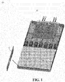
FIG. 1 is a perspective view of an example of an aggregate storage array according to an embodiment; -
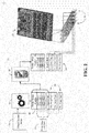
FIG. 2 is an illustration of an example of an authenticated write architecture according to an embodiment; -
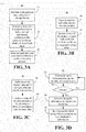
FIG. 3A is a flowchart of an example of a method of operating an application processor according to an embodiment; -
FIG. 3B is a flowchart of an example of a method of operating a signature server according to an embodiment; -
FIG. 3C is a flowchart of an example of a method of operating an aggregate storage array according to an embodiment; -
FIG. 3D is a flowchart of a method of handling drive failures according to an embodiment; -
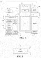
FIG. 4 is a block diagram of an example of a security-enhanced computing system according to an embodiment; and -
FIG. 5 is an illustration of an example of a semiconductor package apparatus according to an embodiment. - Turning now to
FIG. 1 , anaggregate storage array 10 is shown, wherein theaggregate storage array 10 includes a plurality ofstorage devices 12. In one example, theaggregate storage array 10 is an all-flash array (AFA), a redundant array of independent disks (RAID), etc., and each storage device ("drive") 12 is a solid state drive (SSD). Theaggregate storage array 10 may be used to store data payloads such as, for example, financial data (e.g., digitized loan documents), boot images (e.g., for a tenant of a cloud service provider), and so forth. In this regard, theaggregate storage array 10 may replicate data and/or correct errors on a storage block basis, wherein the block size may vary depending on the circumstances (e.g., 256 Kilobytes (KB), 512 KB, 4 Megabytes (MB)). - As will be discussed in greater detail, writes to the
aggregate storage array 10 may be authenticated (e.g., to prevent tampering or other unauthorized modifications of the data payloads) in a manner that does not involve a bidirectional encrypted session between eachstorage device 12 and another verified endpoint (e.g., the entity/component attempting the write operation). More particularly, the data payloads may be partitioned into storage blocks (e.g., pages) that are compatible with the data replication policy and error correction policy (e.g., error correction code/ECC) of theaggregate storage array 10. Additionally, a hash table may be generated to specify how to index into and individually authenticate the storage blocks on a per block basis, wherein theaggregate storage array 10 authenticates a digital signature applied to the hash table. - In one example, the hash table is authenticated on the per block basis by each storage device 12 (e.g., at the drive level) of the
aggregate storage array 10. Accordingly, the hash table may be used to narrow down the data authentication granularity to a single block within the plurality of blocks. Such an approach may enable authentication of the entire data payload to be avoided. The illustratedaggregate storage array 10 therefore provides a relatively simple, efficient and low cost solution to conducting authenticated writes. Thearray 10 may include one or more network interface cards (NICs), switch nodes and/or processors (e.g., compute nodes in a chassis "hot zone") that facilitate modular connectivity to thestorage devices 12. Eachstorage device 12 may be, for example, relatively thin and long (e.g., nineteen inches) ruler shaped SSD (RSSD). In such a case, theaggregate storage array 10 might include thirty-two RSSDs positioned at the front of theaggregate storage array 10 and coupled to the chassis hot zone at the rear of theaggregate storage array 10. The SSDs may therefore be aggregated and presented to a host as a single device to achieve greater storage density. - The
aggregate storage array 10 may be used for a NAND flash memory, three-dimensional (3D) NAND memory array devices, or other memory devices. Non-volatile memory is a storage medium that does not require power to maintain the state of data stored by the medium. In one embodiment, thestorage devices 12 are block addressable memory devices, such as those based on NAND or NOR technologies. A memory device may also include future generation nonvolatile devices, such as a three dimensional (3D) crosspoint memory device, or other byte addressable write-in-place nonvolatile memory devices. In one embodiment, the memory device may be or may include memory devices that use silicon-oxide-nitride-oxide-silicon (SONOS) memory, electrically erasable programmable read-only memory (EEPROM), chalcogenide glass, multi-threshold level NAND flash memory, NOR flash memory, single or multi-level Phase Change Memory (PCM), a resistive memory, nanowire memory, ferroelectric transistor random access memory (FeTRAM), anti-ferroelectric memory, magnetoresistive random access memory (MRAM) memory that incorporates memristor technology, resistive memory including the metal oxide base, the oxygen vacancy base and the conductive bridge Random Access Memory (CB-RAM), or spin transfer torque (STT)-MRAM, a spintronic magnetic junction memory based device, a magnetic tunneling junction (MTJ) based device, a DW (Domain Wall) and SOT (Spin Orbit Transfer) based device, a thiristor based memory device, or a combination of any of the above, or other memory. The memory device may refer to the die itself and/or to a packaged memory product. In some embodiments, 3D crosspoint memory may comprise a transistor-less stackable cross point architecture in which memory cells sit at the intersection of words lines and bit lines and are individually addressable and in which bit storage is based on a change in bulk resistance. In particular embodiments, a memory module with non-volatile memory may comply with one or more standards promulgated by the Joint Electron Device Engineering Council (JEDEC), such as JESD218, JESD219, JESD220-1, JESD223B, JESD223-1, or other suitable standard (the JEDEC standards cited herein are available at jedec.org). -
FIG. 2 shows anauthenticated write architecture 14 in which a binary update image 16 (e.g., data payload) is sent to an application processor 18 (e.g., host processor incorporated into a semiconductor package apparatus, chip, die), which partitions thebinary update image 16 into a plurality of storage blocks 24 (e.g., pages in the illustrated example) and generates (e.g., prefixes) aheader 20 that contains a hash table 22. Theheader 20 may also include other security metadata such as, for example, key information (e.g., data at rest protection keys, public signature verification keys), revision control information (e.g., revision number), encryption algorithm information, and so forth. - A
signature server 26 may digitally sign the hash table 22 to obtain a signedimage 28. The signedimage 28 may be sent to a logical volume (e.g., namespace) in theaggregate storage array 10 via, for example, one or more NICs of theaggregate storage array 10. Additionally, the hash table 22 may be distributed to each of thestorage devices 12 via, for example, a switch node and/or processor/compute node of theaggregate storage array 10. In this regard, if thestorage devices 12 are self-encrypting drives (SEDs) that include built-in high speed encryption controllers/engines, encryption operations may be offloaded to thestorage devices 12 while sharing the same encryption key across multiple storage devices 12 (e.g., facilitating a "horizontal namespace"). Thus, the hash table 22 may be authenticated at the drive level of thearray 10, as will be discussed in greater detail. Upon successful authentication, storage blocks may be distributed todifferent storage devices 12 or replicated acrossmultiple storage devices 12. - Each
storage device 12 may be ECC protected, with all dies (e.g., NVM dies) within aparticular storage device 12 also having XOR protection against die level failure. At the array level, any suitable data reliability and failure recovery solution (e.g., RAID Level 5 or 6) may be used. The compute nodes (e.g., located in the chassis hot zone ofFIG. 1 ) may perform RAID operations and manage the key information that is replicated across all of thestorage devices 12 so that removal of onestorage device 12 does not preclude operation of the entireaggregate storage array 10. - As already noted, the signed
image 28 may be sent (e.g., addressed) to a namespace (e.g., logical volume, not shown) in theaggregate storage array 10. More particularly, the authenticated write may reference a single namespace that spansmultiple storage devices 12 in theaggregate storage array 10. Such an approach may ease tenant migration from one system to another. For example, the single namespace might be allocated to a client and seamlessly migrated from system to system as appropriate. Additionally, a single key may be shared across multipleaggregate storage arrays 10. Accordingly, upon migration thestorage devices 12 may return cipher text instead of plaintext, so that the entire encrypted state is recreated in the new system. Theapplication processor 18, thesignature server 26 and/or theaggregate storage array 10 may be located on the same or different systems/platforms as appropriate. For example, theapplication processor 18 and thesignature server 26 may be located within a hardware security module (HSM) of a data center that includes theaggregate storage array 10. In yet another example, theapplication processor 18, thesignature server 26 and theaggregate storage array 10 may each be remote from one another. -
FIG. 3A shows amethod 30 of operating an application processor. Themethod 30 may generally be implemented in an application processor such as, for example, the application processor 18 (FIG. 2 ), already discussed. More particularly, themethod 30 may be implemented in one or more modules as a set of logic instructions stored in a machine- or computer-readable storage medium such as random access memory (RAM), read only memory (ROM), programmable ROM (PROM), firmware, flash memory, etc., in configurable logic such as, for example, programmable logic arrays (PLAs), field programmable gate arrays (FPGAs), complex programmable logic devices (CPLDs), in fixed-functionality hardware logic using circuit technology such as, for example, application specific integrated circuit (ASIC), complementary metal oxide semiconductor (CMOS) or transistor-transistor logic (TTL) technology, or any combination thereof. - For example, computer program code to carry out operations shown in
method 30 may be written in any combination of one or more programming languages, including an object oriented programming language such as Java, Smalltalk, C++ or the like and conventional procedural programming languages, such as the "C" programming language or similar programming languages. Additionally, logic instructions might include assembler instructions, instruction set architecture (ISA) instructions, machine instructions, machine dependent instructions, microcode, state-setting data, configuration data for integrated circuitry, state information that personalizes electronic circuitry and/or other structural components that are native to hardware (e.g., host processor, central processing unit/CPU, microcontroller, etc.). - Illustrated
processing block 32 provides for partitioning a data payload into a plurality of storage blocks. The storage blocks may be compatible with the block size supported by the data replication policy and/or error correction policy of an aggregate storage array. The data replication policy may generally dictate how individual storage blocks are copied across the drives of the aggregate storage array to enhance resiliency through redundancy. The error correction policy may generally dictate how individual storage blocks are checked for errors (e.g., via parity information) and how errors are remedied (e.g., via recovery of redundant storage blocks). The policies may be documented and/or maintained in any suitable data structure and/or storage medium associated with the array. - A hash table may be generated at processing
block 34, wherein the hash table specifies how to index into and individually authenticate the plurality of storage blocks on a per block basis. More particularly, the hash table may use a hash function to compute an index into the storage blocks, from which a target value can be found. Thus, processingblock 34 may include generating a hash for each storage block and placing the hashes of all of the storage blocks into the hash table/header. Illustratedprocessing block 36 stores the hash table to a header (e.g., prefix) of the data payload. Processingblock 36 may also provide for storing other security metadata such as, for example, key information, revision control information (e.g., revision number), encryption algorithm information, etc., to the header. -
FIG. 3B shows amethod 38 of operating a signature server. Themethod 38 may generally be implemented in a signature server such as, for example, the signature server 26 (FIG. 2 ), already discussed. More particularly, themethod 38 may be implemented in one or more modules as a set of logic instructions stored in a machine- or computer-readable storage medium such as RAM, ROM, PROM, firmware, flash memory, etc., in configurable logic such as, for example, PLAs, FPGAs, CPLDs, in fixed-functionality hardware logic using circuit technology such as, for example, ASIC, CMOS or TTL technology, or any combination thereof. Illustratedprocessing block 40 digitally signs the hash table and the revision number. Processingblock 42 may initiate a write of the digitally signed hash table and revision number to the aggregate storage array. Processingblock 42 may include injecting the signed image into the aggregate storage array, wherein the injection references a single namespace that spans multiple drives in the aggregate storage array. -
FIG. 3C shows amethod 44 of operating an aggregate storage array. Themethod 44 may generally be implemented in an aggregate storage array such as, for example, the aggregate storage array 10 (FIGs. 1-2 ), already discussed. More particularly, themethod 44 may be implemented in one or more modules as a set of logic instructions stored in a machine- or computer-readable storage medium such as RAM, ROM, PROM, firmware, flash memory, etc., in configurable logic such as, for example, PLAs, FPGAs, CPLDs, in fixed-functionality hardware logic using circuit technology such as, for example, ASIC, CMOS or TTL technology, or any combination thereof. - Illustrated
processing block 46 provides for authenticating the digital signature of a hash table and a revision number. In one example, processingblock 46, which may use a public signature verification key, authenticates the hash table on a per block basis at the drive level of the aggregate storage array. In such a case, the compute nodes of the aggregate storage array may distribute/forward the hash table to the drives without re-signing the hash table. Such an approach may significantly enhance efficiency. In one example, the authentication is conducted at least partly based on the signed revision number in the header of the data payload. In this regard, the plurality of drives may ensure that the signed revision number is greater than or equal to the current security version number. Such an approach may prevent unauthorized rollback to a previous version of a signed data payload. - Processing
block 48 may conduct a write of portions of the data payload to the plurality of drives in accordance with the hash table. More particularly, processingblock 48 may place any number of storage blocks (e.g., pages) of payload data into any one of the plurality of drives that contain the verified hash table, without resigning the storage blocks. Thus, processingblock 48 may distribute storage blocks to different drives and/or replicate storage blocks across multiple drives. Moreover, processingblock 48 may be repeated for subsequent writes of one or more additional storage blocks (e.g., pages) to the aggregate storage array in accordance with the hash table. For example, as additional storage blocks become available, the same relatively small hash table may be used to authenticate any number of storage blocks received. As already noted, processingblock 48 may include replicating one or more storage blocks across multiple drives in the aggregate storage array. An example data payload header may include, but is not limited to: key information, revision control information, encryption algorithm information, etc., or any combination thereof. -
FIG. 3D shows amethod 50 of handling drive failures. Themethod 50 may generally be implemented in an aggregate storage array such as, for example, the aggregate storage array 10 (FIGs. 1-2 ), already discussed. More particularly, themethod 50 may be implemented in one or more modules as a set of logic instructions stored in a machine- or computer-readable storage medium such as RAM, ROM, PROM, firmware, flash memory, etc., in configurable logic such as, for example, PLAs, FPGAs, CPLDs, in fixed-functionality hardware logic using circuit technology such as, for example, ASIC, CMOS or TTL technology, or any combination thereof. - Illustrated
processing block 52 determines parity information across the plurality of storage blocks. The parity information may be determined by, for example, conducting an XOR computation over the affected pages (RAID 5), conducting an ECC based computation, and so forth. A determination may be made at processingblock 54 as to whether a failure has occurred in one or more drives in the aggregate storage array. Processingblock 54 may use a suitable ECC process on a per storage block basis. If a failure is detected, the parity information may be recovered at processingblock 56 in response to the failure. Additionally, the storage block(s) in the drive(s) containing the failure may be reconstructed at processingblock 58 based on the recovered parity information. More particularly, if a drive fails, theprocessing block 58 may unlock the remaining drives and rebuild the parity information in the new drive. In addition, theprocessing block 58 may provision the new drive with the appropriate public signature verification keys and data at rest protection keys. The provisioning operation may be protected through a bi-directional authentication mechanism with pre-provisioned certificates or pre-shared keys. If no failure is detected at processingblock 54, the illustrated method returns to processingblock 52. - Turning now to
FIG. 4 , a security-enhancedcomputing system 60 is shown. Thecomputing system 60 may generally be part of an electronic device/platform having computing functionality (e.g., personal digital assistant/PDA, notebook computer, tablet computer, server), communications functionality (e.g., smart phone), imaging functionality, media playing functionality (e.g., smart television/TV), wearable functionality (e.g., watch, eyewear, headwear, footwear, jewelry), vehicular functionality (e.g., car, truck, motorcycle), etc., or any combination thereof. In the illustrated example, thesystem 60 includes apower supply 62 to provide power to thesystem 60 and a host processor 64 (e.g., central processing unit/CPU) having an integrated memory controller (IMC) 66 that is coupled to asystem memory 68. - The illustrated
system 60 also includes an input output (IO)module 70 implemented together with theprocessor 64 on asemiconductor die 72 as a system on chip (SoC), wherein theIO module 70 functions as a host device and may communicate with, for example, a display 74 (e.g., touch screen, liquid crystal display/LCD, light emitting diode/LED display), anetwork controller 76, and an aggregate storage array 78 (e.g., AFA, RAID). The illustratedsystem memory 68 includes a set ofinstructions 80, which when executed by thehost processor 64, cause thesystem 60 to perform one or more aspects of the method 30 (FIG. 3A ) and/or the method 38 (FIG. 3B ). Thus, thehost processor 64 may function as an application processor and/or signature server that outputs digitally signed data payloads and hash tables as described herein. Theinstructions 80 may also be implemented in a semiconductor package apparatus (e.g., chip, die) as configurable logic and/or fixed-functionality hardware logic. - The
aggregate storage array 78 may include one or more network controllers 82 (e.g., NICs), one ormore switch nodes 84, one ormore compute nodes 86 and a plurality of drives 90 (e.g., SSDs). The network controller(s) 82 may receive a hash table and a data payload, wherein the data payload is partitioned into a plurality of storage blocks and the hash table specifies how to index into and individually authenticate the plurality of storage blocks. Theaggregate storage array 78 may also include alocal memory 92 that stores a set ofinstructions 94, which when executed by the compute node(s) 86, cause thedrives 90 of theaggregate storage array 78 to perform one or more aspects of the method 44 (FIG. 3C ) and/or the method 50 (FIG. 3D ), already discussed. Thus, thearray 78 may authenticate the hash table and data payload, and write the data payload to thedrives 90, as described herein. Theinstructions 94 may also be implemented in a semiconductor package apparatus (e.g., chip, die) as configurable logic and/or fixed-functionality hardware logic. The illustratedaggregate storage array 78 also includes apower supply 88 to provide power to theaggregate storage array 78, although thesystem power supply 62 may alternatively provide power to theaggregate storage array 78. -
FIG. 5 shows a semiconductor package apparatus 96 (e.g., chip, die) that includes a substrate 98 (e.g., silicon, sapphire, gallium arsenide) and logic 100 (e.g., transistor array and other integrated circuit/IC components) coupled to thesubstrate 98. Thelogic 100, which may be implemented in configurable logic and/or fixed-functionality logic hardware, may generally implement one or more aspects of the method 30 (FIG. 3A ), the method 38 (FIG. 3B ), the method 44 (FIG. 3C ) and/or the method 50 (FIG. 3D ), already discussed. - Example 1 may include an aggregate storage array comprising a plurality of drives, a network controller to receive a hash table and a data payload, wherein the data payload is to be partitioned into a plurality of storage blocks and the hash table is to specify how to index into and individually authenticate the plurality of storage blocks on a per block basis, and logic to authenticate a digital signature of the hash table and the data payload, and conduct a write of the data payload to the plurality of drives in accordance with the hash table.
- Example 2 may include the aggregate storage array of Example 1, wherein the plurality of storage blocks are to be compatible with a block size supported by one or more of a data replication policy or an error correction policy of the aggregate storage array.
- Example 3 may include the aggregate storage array of Example 1, wherein the write is to reference a single namespace that spans multiple drives in the aggregate storage array.
- Example 4 may include the aggregate storage array of Example 1, wherein the hash table is to be authenticated on the per block basis at a drive level of the aggregate storage array based at least in part on a revision number in a header of the data payload.
- Example 5 may include the aggregate storage array of any one of Examples 1 to 4, wherein the logic is to determine parity information across the plurality of storage blocks.
- Example 6 may include the aggregate storage array of Example 5, wherein the logic is to detect a failure in one or more drives in the aggregate storage array, wherein the write is to include replicating one or more storage blocks in the one or more drives containing the failure across multiple drives in the aggregate storage array, recover the parity information in response to the failure, and reconstruct the one or more storage blocks in the one or more drives containing the failure based on the recovered parity information.
- Example 7 may include at least one computer readable storage medium comprising a set of instructions, which when executed by an aggregate storage array, cause the aggregate storage array to authenticate a digital signature of a hash table and a data payload, wherein the data payload is to be partitioned into a plurality of storage blocks and the hash table is to specify how to index into and individually authenticate the plurality of storage blocks on a per block basis, and conduct a write of the data payload to a plurality of drives in an aggregate storage array in accordance with the hash table.
- Example 8 may include the at least one computer readable storage medium of Example 7, wherein the plurality of storage blocks are to be compatible with a block size supported by one or more of a data replication policy or an error correction policy of the aggregate storage array.
- Example 9 may include the at least one computer readable storage medium of Example 7, wherein the write is to reference a single namespace that spans multiple drives in the aggregate storage array.
- Example 10 may include the at least one computer readable storage medium of Example 7, wherein the hash table is to be authenticated on the per block basis at a drive level of the aggregate storage array based at least in part on a revision number in a header of the data payload.
- Example 11 may include the at least one computer readable storage medium of any one of Examples 7 to 10, wherein the instructions, when executed, cause the aggregate storage array to determine parity information across the plurality of storage blocks.
- Example 12 may include the at least one computer readable storage medium of Example 11, wherein the instructions, when executed, cause the aggregate storage array to detect a failure in one or more drives in the aggregate storage array, wherein the write is to include replicating one or more storage blocks in the one or more drives containing the failure across multiple drives in the aggregate storage array, recover the parity information in response to the failure, and reconstruct the one or more storage blocks in the one or more drives containing the failure based on the recovered parity information.
- Example 13 may include a semiconductor package apparatus comprising a substrate, and logic coupled to the substrate, wherein the logic is implemented in one or more of configurable logic or fixed-functionality hardware logic, the logic to digitally sign a hash table and a data payload, wherein the data payload is to be partitioned into a plurality of storage blocks and the hash table is to specify how to index into and individually authenticate the plurality of storage blocks on a per block basis, and initiate a write of the digitally signed hash table and data payload to an aggregate storage array.
- Example 14 may include the semiconductor package apparatus of Example 13, wherein the plurality of storage blocks are to be compatible with a block size supported by one or more of a data replication policy or an error correction policy of the aggregate storage array.
- Example 15 may include the semiconductor package apparatus of Example 13, wherein the write is to reference a single namespace that spans multiple drives in the aggregate storage array.
- Example 16 may include the semiconductor package apparatus of Example 13, wherein the logic is to conduct a subsequent write of one or more additional storage blocks to the aggregate storage array in accordance with the hash table.
- Example 17 may include the semiconductor package apparatus of any one of Examples 13 to 16, wherein the logic is to partition the data payload into the plurality of storage blocks, generate the hash table, and store the hash table and a revision number to a header of the data payload.
- Example 18 may include the semiconductor package apparatus of Example 17, wherein the logic is to store include one or more of key information, revision control information or encryption algorithm information to the header.
- Example 19 may include at least one computer readable storage medium comprising a set of instructions, which when executed by a computing system, cause the computing system to digitally sign a hash table and a data payload, wherein the data payload is to be partitioned into a plurality of storage blocks and the hash table is to specify how to index into and individually authenticate the plurality of storage blocks on a per block basis, and initiate a write of the digitally signed hash table and data payload to an aggregate storage array.
- Example 20 may include the at least one computer readable storage medium of Example 19, wherein the plurality of storage blocks are to be compatible with a block size supported by one or more of a data replication policy or an error correction policy of the aggregate storage array.
- Example 21 may include the at least one computer readable storage medium of Example 19, wherein the write is to reference a single namespace that spans multiple drives in the aggregate storage array.
- Example 22 may include the at least one computer readable storage medium of Example 19, wherein the instructions, when executed, cause the computing system to conduct a subsequent write of one or more additional storage blocks to the aggregate storage array in accordance with the hash table.
- Example 23 may include the at least one computer readable storage medium of any one of Examples 19 to 22, wherein the instructions, when executed, cause the computing system to partition the data payload into the plurality of storage blocks, generate the hash table, and store the hash table and a revision number to a header of the data payload.
- Example 24 may include the at least one computer readable storage medium of Example 23, wherein the instructions, when executed, cause the computing device to store one or more of key information, revision control information or encryption algorithm information to the header.
- Example 25 may include a method of operating a signature server, comprising digitally signing a hash table and a data payload, wherein the data payload is partitioned into a plurality of storage blocks and the hash table specifies how to index into and individually authenticate the plurality of storage blocks on a per block basis, and initiating a write of the digitally signed hash table and data payload to an aggregate storage array.
- Example 26 may include the method of Example 25, wherein the plurality of storage blocks are compatible with a block size supported by one or more of a data replication policy or an error correction policy of the aggregate storage array.
- Example 27 may include the method of Example 25, wherein the write references a single namespace that spans multiple drives in the aggregate storage array.
- Example 28 may include the method of Example 25, further including conducting a subsequent write of one or more additional storage blocks to the aggregate storage array in accordance with the hash table.
- Example 29 may include the method of any one of Examples 25 to 28, further including partitioning the data payload into the plurality of storage blocks, generating the hash table, and storing the hash table and a revision number to a header of the data payload.
- Example 30 may include the method of Example 29, further including storing one or more of key information, revision control information or encryption algorithm information to the header.
- Example 31 may include a method of operating an aggregate storage array, comprising authenticating a digital signature of a hash table and a data payload, wherein the data payload is partitioned into a plurality of storage blocks and the hash table specifies how to index into and individually authenticate the plurality of storage blocks on a per block basis, and conducting a write of the data payload to a plurality of drives in the aggregate storage array in accordance with the hash table.
- Example 32 may include the method of Example 31, wherein the plurality of storage blocks are compatible with a block size supported by one or more of a data replication policy or an error correction policy of the aggregate storage array.
- Example 33 may include the method of Example 31, wherein the write references a single namespace that spans multiple drives in the aggregate storage array.
- Example 34 may include the method of Example 31, wherein the hash table is authenticated on the per block basis at a drive level of the aggregate storage array based at least in part on a revision number in a header of the data payload.
- Example 35 may include the method of any one of Examples 31 to 34, further including determining parity information across the plurality of storage blocks.
- Example 36 may include the method of Example 35, further including detecting a failure in one or more drives in the aggregate storage array, wherein the write includes replicating one or more storage blocks in the one or more drives containing the failure across multiple drives in the aggregate storage array, recovering the parity information in response to the failure, and reconstructing the one or more storage blocks in the one or more drives containing the failure based on the recovered parity information.
- Example 37 may include a signature server apparatus comprising means for performing the method of any one of Examples 25 to 29.
- Example 38 may include an aggregate storage array comprising means for performing the method of any one of Examples 31 to 34.
- Technology described herein may therefore provide authenticated writes to logical volumes composed of multiple, aggregated storage volumes. Accordingly, storage appliances may have enhanced resilience against malware attacks. Technology described herein may also enable robust and secure recovery of data contained within an aggregate logical volume when one or many of the physical member disks have failed.
- Embodiments are applicable for use with all types of semiconductor integrated circuit ("IC") chips. Examples of these IC chips include but are not limited to processors, controllers, chipset components, programmable logic arrays (PLAs), memory chips, network chips, systems on chip (SoCs), SSD/NAND controller ASICs, and the like. In addition, in some of the drawings, signal conductor lines are represented with lines. Some may be different, to indicate more constituent signal paths, have a number label, to indicate a number of constituent signal paths, and/or have arrows at one or more ends, to indicate primary information flow direction. This, however, should not be construed in a limiting manner. Rather, such added detail may be used in connection with one or more exemplary embodiments to facilitate easier understanding of a circuit. Any represented signal lines, whether or not having additional information, may actually comprise one or more signals that may travel in multiple directions and may be implemented with any suitable type of signal scheme, e.g., digital or analog lines implemented with differential pairs, optical fiber lines, and/or single-ended lines.
- Example sizes/models/values/ranges may have been given, although embodiments are not limited to the same. As manufacturing techniques (e.g., photolithography) mature over time, it is expected that devices of smaller size could be manufactured. In addition, well known power/ground connections to IC chips and other components may or may not be shown within the figures, for simplicity of illustration and discussion, and so as not to obscure certain aspects of the embodiments. Further, arrangements may be shown in block diagram form in order to avoid obscuring embodiments, and also in view of the fact that specifics with respect to implementation of such block diagram arrangements are highly dependent upon the platform within which the embodiment is to be implemented, i.e., such specifics should be well within purview of one skilled in the art. Where specific details (e.g., circuits) are set forth in order to describe example embodiments, it should be apparent to one skilled in the art that embodiments can be practiced without, or with variation of, these specific details. The description is thus to be regarded as illustrative instead of limiting.
- The term "coupled" may be used herein to refer to any type of relationship, direct or indirect, between the components in question, and may apply to electrical, mechanical, fluid, optical, electromagnetic, electromechanical or other connections. In addition, the terms "first", "second", etc. may be used herein only to facilitate discussion, and carry no particular temporal or chronological significance unless otherwise indicated.
- As used in this application and in the claims, a list of items joined by the term "one or more of' may mean any combination of the listed terms. For example, the phrases "one or more of A, B or C" may mean A, B, C; A and B; A and C; B and C; or A, B and C.
- Those skilled in the art will appreciate from the foregoing description that the broad techniques of the embodiments can be implemented in a variety of forms. Therefore, while the embodiments have been described in connection with particular examples thereof, the true scope of the embodiments should not be so limited since other modifications will become apparent to the skilled practitioner upon a study of the drawings, specification, and following claims.
Claims (13)
- An aggregate storage array comprising:a plurality of drives;a network controller to receive a hash table and a data payload, wherein the data payload is to be partitioned into a plurality of storage blocks and the hash table is to specify how to index into and individually authenticate the plurality of storage blocks on a per block basis; andlogic to:authenticate a digital signature of the hash table and the data payload, andconduct a write of the data payload to the plurality of drives in accordance with the hash table.
- The aggregate storage array of claim 1, wherein the plurality of storage blocks are to be compatible with a block size supported by one or more of a data replication policy or an error correction policy of the aggregate storage array.
- The aggregate storage array of claim 1, wherein the write is to reference a single namespace that spans multiple drives in the aggregate storage array.
- The aggregate storage array of claim 1, wherein the hash table is to be authenticated on the per block basis at a drive level of the aggregate storage array based at least in part on a revision number in a header of the data payload.
- The aggregate storage array of any one of claims 1 to 4, wherein the logic is to determine parity information across the plurality of storage blocks.
- The aggregate storage array of claim 5, wherein the logic is to:detect a failure in one or more drives in the aggregate storage array, wherein the write is to include replicating one or more storage blocks in the one or more drives containing the failure across multiple drives in the aggregate storage array;recover the parity information in response to the failure; andreconstruct the one or more storage blocks in the one or more drives containing the failure based on the recovered parity information.
- At least one computer readable storage medium comprising a set of instructions, which when executed by an aggregate storage array, cause the aggregate storage array to:authenticate a digital signature of a hash table and a data payload, wherein the data payload is to be partitioned into a plurality of storage blocks and the hash table is to specify how to index into and individually authenticate the plurality of storage blocks on a per block basis; andconduct a write of the data payload to a plurality of drives in an aggregate storage array in accordance with the hash table.
- The at least one computer readable storage medium of claim 7, wherein the plurality of storage blocks are to be compatible with a block size supported by one or more of a data replication policy or an error correction policy of the aggregate storage array.
- The at least one computer readable storage medium of claim 7, wherein the write is to reference a single namespace that spans multiple drives in the aggregate storage array.
- The at least one computer readable storage medium of claim 7, wherein the hash table is to be authenticated on the per block basis at a drive level of the aggregate storage array based at least in part on a revision number in a header of the data payload.
- The at least one computer readable storage medium of any one of claims 7 to 10, wherein the instructions, when executed, cause the aggregate storage array to determine parity information across the plurality of storage blocks.
- The at least one computer readable storage medium of claim 11, wherein the instructions, when executed, cause the aggregate storage array to:detect a failure in one or more drives in the aggregate storage array, wherein the write is to include replicating one or more storage blocks in the one or more drives containing the failure across multiple drives in the aggregate storage array;recover the parity information in response to the failure; andreconstruct the one or more storage blocks in the one or more drives containing the failure based on the recovered parity information.
- A method of operating a signature server, comprising:digitally signing a hash table and a data payload, wherein the data payload is partitioned into a plurality of storage blocks and the hash table specifies how to index into and individually authenticate the plurality of storage blocks on a per block basis; andinitiating a write of the digitally signed hash table and data payload to an aggregate storage array.
Applications Claiming Priority (1)
| Application Number | Priority Date | Filing Date | Title |
|---|---|---|---|
| US15/636,788 US10592477B2 (en) | 2017-06-29 | 2017-06-29 | Performing authenticated writes across aggregate storage volumes |
Publications (2)
| Publication Number | Publication Date |
|---|---|
| EP3422242A1 true EP3422242A1 (en) | 2019-01-02 |
| EP3422242B1 EP3422242B1 (en) | 2023-06-07 |
Family
ID=62635975
Family Applications (1)
| Application Number | Title | Priority Date | Filing Date |
|---|---|---|---|
| EP18174968.0A Active EP3422242B1 (en) | 2017-06-29 | 2018-05-29 | Performing authenticated writes across aggregate storage volumes |
Country Status (2)
| Country | Link |
|---|---|
| US (1) | US10592477B2 (en) |
| EP (1) | EP3422242B1 (en) |
Citations (4)
| Publication number | Priority date | Publication date | Assignee | Title |
|---|---|---|---|---|
| US20020194209A1 (en) * | 2001-03-21 | 2002-12-19 | Bolosky William J. | On-disk file format for a serverless distributed file system |
| US20080294696A1 (en) * | 2007-05-22 | 2008-11-27 | Yuval Frandzel | System and method for on-the-fly elimination of redundant data |
| US20100062844A1 (en) * | 2003-03-05 | 2010-03-11 | Bally Gaming, Inc. | Authentication and validation systems for gaming devices |
| US20160191250A1 (en) * | 2014-12-31 | 2016-06-30 | Nexenta Systems, Inc. | Read-Modify-Write Processing of Chunks at the Storage Server Level in a Distributed Object Storage System |
Family Cites Families (7)
| Publication number | Priority date | Publication date | Assignee | Title |
|---|---|---|---|---|
| US8706914B2 (en) * | 2007-04-23 | 2014-04-22 | David D. Duchesneau | Computing infrastructure |
| US8819452B2 (en) * | 2009-11-25 | 2014-08-26 | Cleversafe, Inc. | Efficient storage of encrypted data in a dispersed storage network |
| US8566354B2 (en) * | 2010-04-26 | 2013-10-22 | Cleversafe, Inc. | Storage and retrieval of required slices in a dispersed storage network |
| US8782227B2 (en) * | 2010-06-22 | 2014-07-15 | Cleversafe, Inc. | Identifying and correcting an undesired condition of a dispersed storage network access request |
| US20150288680A1 (en) * | 2014-04-02 | 2015-10-08 | Cleversafe, Inc. | Distributing registry information in a dispersed storage network |
| US10229281B2 (en) | 2015-10-13 | 2019-03-12 | Mcafee, Llc | Remote provisioning and authenticated writes to secure storage devices |
| US20170208125A1 (en) * | 2016-01-19 | 2017-07-20 | Hope Bay Technologies, Inc | Method and apparatus for data prefetch in cloud based storage system |
-
2017
- 2017-06-29 US US15/636,788 patent/US10592477B2/en active Active
-
2018
- 2018-05-29 EP EP18174968.0A patent/EP3422242B1/en active Active
Patent Citations (4)
| Publication number | Priority date | Publication date | Assignee | Title |
|---|---|---|---|---|
| US20020194209A1 (en) * | 2001-03-21 | 2002-12-19 | Bolosky William J. | On-disk file format for a serverless distributed file system |
| US20100062844A1 (en) * | 2003-03-05 | 2010-03-11 | Bally Gaming, Inc. | Authentication and validation systems for gaming devices |
| US20080294696A1 (en) * | 2007-05-22 | 2008-11-27 | Yuval Frandzel | System and method for on-the-fly elimination of redundant data |
| US20160191250A1 (en) * | 2014-12-31 | 2016-06-30 | Nexenta Systems, Inc. | Read-Modify-Write Processing of Chunks at the Storage Server Level in a Distributed Object Storage System |
Also Published As
| Publication number | Publication date |
|---|---|
| EP3422242B1 (en) | 2023-06-07 |
| US10592477B2 (en) | 2020-03-17 |
| US20190005063A1 (en) | 2019-01-03 |
Similar Documents
| Publication | Publication Date | Title |
|---|---|---|
| CN106470102B (en) | Cryptographic device, storage device with cryptographic device, and encryption and decryption methods thereof | |
| TWI826844B (en) | Memory device having safety boot capability | |
| US12316736B2 (en) | Device for supporting homomorphic encryption operation and operating method thereof | |
| US11669644B2 (en) | Storage device and data destruction method thereof | |
| US9864654B2 (en) | Detecting data indicated as being uncorrectable at a data storage device | |
| US11669395B2 (en) | Memory system including field programmable gate array (FPGA) and method of operating same | |
| CN113127843B (en) | Double wrapping for verification | |
| US10255200B2 (en) | Data storage device and method of operation using multiple security protocols | |
| US20250219826A1 (en) | Secure data storage with a dynamically generated key | |
| CN113348456A (en) | Memory device with cryptographic components | |
| US12368578B2 (en) | Secret management in distributed systems using passphrases | |
| US12566837B2 (en) | Multi-chip for performing chiplet security authentication and method of manufacturing the same | |
| US20170180116A1 (en) | End-to-end protection scheme involving encrypted memory and storage | |
| TW202403773A (en) | Semiconductor device, and system and method for managing secure operations in the same | |
| EP3422242B1 (en) | Performing authenticated writes across aggregate storage volumes | |
| US11863664B2 (en) | Method of performing key exchange for security operation in storage device and method of performing authority transfer in storage device using the same | |
| US12074983B2 (en) | Trusted computing device and operating method thereof | |
| TW202011248A (en) | Data storage device and operating method therefor | |
| WO2023035136A1 (en) | Data protection method for memory, and storage apparatus thereof | |
| US12436691B2 (en) | Data storage device and method for hiding tweak generation latency | |
| US12242740B2 (en) | Data storage device and method for hiding tweak generation latency | |
| KR20230068945A (en) | Device for supporting homomorphic encryption operation and operating method thereof | |
| CN118898089A (en) | Data storage device and method for hiding adjustment generation latency | |
| KR20230067436A (en) | Trusted computing device and operating method thereof | |
| KR20230068250A (en) | Storage device, storage system having the same and operating method thereof |
Legal Events
| Date | Code | Title | Description |
|---|---|---|---|
| PUAI | Public reference made under article 153(3) epc to a published international application that has entered the european phase |
Free format text: ORIGINAL CODE: 0009012 |
|
| STAA | Information on the status of an ep patent application or granted ep patent |
Free format text: STATUS: THE APPLICATION HAS BEEN PUBLISHED |
|
| AK | Designated contracting states |
Kind code of ref document: A1 Designated state(s): AL AT BE BG CH CY CZ DE DK EE ES FI FR GB GR HR HU IE IS IT LI LT LU LV MC MK MT NL NO PL PT RO RS SE SI SK SM TR |
|
| AX | Request for extension of the european patent |
Extension state: BA ME |
|
| STAA | Information on the status of an ep patent application or granted ep patent |
Free format text: STATUS: REQUEST FOR EXAMINATION WAS MADE |
|
| 17P | Request for examination filed |
Effective date: 20190702 |
|
| RBV | Designated contracting states (corrected) |
Designated state(s): AL AT BE BG CH CY CZ DE DK EE ES FI FR GB GR HR HU IE IS IT LI LT LU LV MC MK MT NL NO PL PT RO RS SE SI SK SM TR |
|
| STAA | Information on the status of an ep patent application or granted ep patent |
Free format text: STATUS: EXAMINATION IS IN PROGRESS |
|
| 17Q | First examination report despatched |
Effective date: 20201113 |
|
| RIC1 | Information provided on ipc code assigned before grant |
Ipc: H04L 67/1097 20220101ALN20220511BHEP Ipc: G06F 21/64 20130101AFI20220511BHEP |
|
| RIC1 | Information provided on ipc code assigned before grant |
Ipc: H04L 67/1097 20220101ALN20220516BHEP Ipc: G06F 21/64 20130101AFI20220516BHEP |
|
| GRAP | Despatch of communication of intention to grant a patent |
Free format text: ORIGINAL CODE: EPIDOSNIGR1 |
|
| STAA | Information on the status of an ep patent application or granted ep patent |
Free format text: STATUS: GRANT OF PATENT IS INTENDED |
|
| RIC1 | Information provided on ipc code assigned before grant |
Ipc: H04L 67/1097 20220101ALN20220614BHEP Ipc: G06F 21/64 20130101AFI20220614BHEP |
|
| INTG | Intention to grant announced |
Effective date: 20220630 |
|
| GRAJ | Information related to disapproval of communication of intention to grant by the applicant or resumption of examination proceedings by the epo deleted |
Free format text: ORIGINAL CODE: EPIDOSDIGR1 |
|
| STAA | Information on the status of an ep patent application or granted ep patent |
Free format text: STATUS: EXAMINATION IS IN PROGRESS |
|
| INTC | Intention to grant announced (deleted) | ||
| GRAP | Despatch of communication of intention to grant a patent |
Free format text: ORIGINAL CODE: EPIDOSNIGR1 |
|
| STAA | Information on the status of an ep patent application or granted ep patent |
Free format text: STATUS: GRANT OF PATENT IS INTENDED |
|
| RIC1 | Information provided on ipc code assigned before grant |
Ipc: H04L 67/1097 20220101ALN20221121BHEP Ipc: G06F 21/64 20130101AFI20221121BHEP |
|
| INTG | Intention to grant announced |
Effective date: 20221221 |
|
| GRAS | Grant fee paid |
Free format text: ORIGINAL CODE: EPIDOSNIGR3 |
|
| GRAA | (expected) grant |
Free format text: ORIGINAL CODE: 0009210 |
|
| STAA | Information on the status of an ep patent application or granted ep patent |
Free format text: STATUS: THE PATENT HAS BEEN GRANTED |
|
| AK | Designated contracting states |
Kind code of ref document: B1 Designated state(s): AL AT BE BG CH CY CZ DE DK EE ES FI FR GB GR HR HU IE IS IT LI LT LU LV MC MK MT NL NO PL PT RO RS SE SI SK SM TR |
|
| REG | Reference to a national code |
Ref country code: GB Ref legal event code: FG4D |
|
| REG | Reference to a national code |
Ref country code: CH Ref legal event code: EP Ref country code: AT Ref legal event code: REF Ref document number: 1577182 Country of ref document: AT Kind code of ref document: T Effective date: 20230615 Ref country code: DE Ref legal event code: R096 Ref document number: 602018050701 Country of ref document: DE |
|
| P01 | Opt-out of the competence of the unified patent court (upc) registered |
Effective date: 20230616 |
|
| REG | Reference to a national code |
Ref country code: NL Ref legal event code: FP |
|
| REG | Reference to a national code |
Ref country code: LT Ref legal event code: MG9D |
|
| PG25 | Lapsed in a contracting state [announced via postgrant information from national office to epo] |
Ref country code: SE Free format text: LAPSE BECAUSE OF FAILURE TO SUBMIT A TRANSLATION OF THE DESCRIPTION OR TO PAY THE FEE WITHIN THE PRESCRIBED TIME-LIMIT Effective date: 20230607 Ref country code: NO Free format text: LAPSE BECAUSE OF FAILURE TO SUBMIT A TRANSLATION OF THE DESCRIPTION OR TO PAY THE FEE WITHIN THE PRESCRIBED TIME-LIMIT Effective date: 20230907 Ref country code: ES Free format text: LAPSE BECAUSE OF FAILURE TO SUBMIT A TRANSLATION OF THE DESCRIPTION OR TO PAY THE FEE WITHIN THE PRESCRIBED TIME-LIMIT Effective date: 20230607 |
|
| REG | Reference to a national code |
Ref country code: AT Ref legal event code: MK05 Ref document number: 1577182 Country of ref document: AT Kind code of ref document: T Effective date: 20230607 |
|
| PG25 | Lapsed in a contracting state [announced via postgrant information from national office to epo] |
Ref country code: RS Free format text: LAPSE BECAUSE OF FAILURE TO SUBMIT A TRANSLATION OF THE DESCRIPTION OR TO PAY THE FEE WITHIN THE PRESCRIBED TIME-LIMIT Effective date: 20230607 Ref country code: LV Free format text: LAPSE BECAUSE OF FAILURE TO SUBMIT A TRANSLATION OF THE DESCRIPTION OR TO PAY THE FEE WITHIN THE PRESCRIBED TIME-LIMIT Effective date: 20230607 Ref country code: LT Free format text: LAPSE BECAUSE OF FAILURE TO SUBMIT A TRANSLATION OF THE DESCRIPTION OR TO PAY THE FEE WITHIN THE PRESCRIBED TIME-LIMIT Effective date: 20230607 Ref country code: HR Free format text: LAPSE BECAUSE OF FAILURE TO SUBMIT A TRANSLATION OF THE DESCRIPTION OR TO PAY THE FEE WITHIN THE PRESCRIBED TIME-LIMIT Effective date: 20230607 Ref country code: GR Free format text: LAPSE BECAUSE OF FAILURE TO SUBMIT A TRANSLATION OF THE DESCRIPTION OR TO PAY THE FEE WITHIN THE PRESCRIBED TIME-LIMIT Effective date: 20230908 |
|
| PG25 | Lapsed in a contracting state [announced via postgrant information from national office to epo] |
Ref country code: FI Free format text: LAPSE BECAUSE OF FAILURE TO SUBMIT A TRANSLATION OF THE DESCRIPTION OR TO PAY THE FEE WITHIN THE PRESCRIBED TIME-LIMIT Effective date: 20230607 |
|
| PG25 | Lapsed in a contracting state [announced via postgrant information from national office to epo] |
Ref country code: SK Free format text: LAPSE BECAUSE OF FAILURE TO SUBMIT A TRANSLATION OF THE DESCRIPTION OR TO PAY THE FEE WITHIN THE PRESCRIBED TIME-LIMIT Effective date: 20230607 |
|
| PG25 | Lapsed in a contracting state [announced via postgrant information from national office to epo] |
Ref country code: IS Free format text: LAPSE BECAUSE OF FAILURE TO SUBMIT A TRANSLATION OF THE DESCRIPTION OR TO PAY THE FEE WITHIN THE PRESCRIBED TIME-LIMIT Effective date: 20231007 |
|
| PG25 | Lapsed in a contracting state [announced via postgrant information from national office to epo] |
Ref country code: SM Free format text: LAPSE BECAUSE OF FAILURE TO SUBMIT A TRANSLATION OF THE DESCRIPTION OR TO PAY THE FEE WITHIN THE PRESCRIBED TIME-LIMIT Effective date: 20230607 Ref country code: SK Free format text: LAPSE BECAUSE OF FAILURE TO SUBMIT A TRANSLATION OF THE DESCRIPTION OR TO PAY THE FEE WITHIN THE PRESCRIBED TIME-LIMIT Effective date: 20230607 Ref country code: RO Free format text: LAPSE BECAUSE OF FAILURE TO SUBMIT A TRANSLATION OF THE DESCRIPTION OR TO PAY THE FEE WITHIN THE PRESCRIBED TIME-LIMIT Effective date: 20230607 Ref country code: PT Free format text: LAPSE BECAUSE OF FAILURE TO SUBMIT A TRANSLATION OF THE DESCRIPTION OR TO PAY THE FEE WITHIN THE PRESCRIBED TIME-LIMIT Effective date: 20231009 Ref country code: IS Free format text: LAPSE BECAUSE OF FAILURE TO SUBMIT A TRANSLATION OF THE DESCRIPTION OR TO PAY THE FEE WITHIN THE PRESCRIBED TIME-LIMIT Effective date: 20231007 Ref country code: EE Free format text: LAPSE BECAUSE OF FAILURE TO SUBMIT A TRANSLATION OF THE DESCRIPTION OR TO PAY THE FEE WITHIN THE PRESCRIBED TIME-LIMIT Effective date: 20230607 Ref country code: CZ Free format text: LAPSE BECAUSE OF FAILURE TO SUBMIT A TRANSLATION OF THE DESCRIPTION OR TO PAY THE FEE WITHIN THE PRESCRIBED TIME-LIMIT Effective date: 20230607 Ref country code: AT Free format text: LAPSE BECAUSE OF FAILURE TO SUBMIT A TRANSLATION OF THE DESCRIPTION OR TO PAY THE FEE WITHIN THE PRESCRIBED TIME-LIMIT Effective date: 20230607 |
|
| PG25 | Lapsed in a contracting state [announced via postgrant information from national office to epo] |
Ref country code: PL Free format text: LAPSE BECAUSE OF FAILURE TO SUBMIT A TRANSLATION OF THE DESCRIPTION OR TO PAY THE FEE WITHIN THE PRESCRIBED TIME-LIMIT Effective date: 20230607 |
|
| REG | Reference to a national code |
Ref country code: DE Ref legal event code: R097 Ref document number: 602018050701 Country of ref document: DE |
|
| PLBE | No opposition filed within time limit |
Free format text: ORIGINAL CODE: 0009261 |
|
| STAA | Information on the status of an ep patent application or granted ep patent |
Free format text: STATUS: NO OPPOSITION FILED WITHIN TIME LIMIT |
|
| PG25 | Lapsed in a contracting state [announced via postgrant information from national office to epo] |
Ref country code: DK Free format text: LAPSE BECAUSE OF FAILURE TO SUBMIT A TRANSLATION OF THE DESCRIPTION OR TO PAY THE FEE WITHIN THE PRESCRIBED TIME-LIMIT Effective date: 20230607 |
|
| PG25 | Lapsed in a contracting state [announced via postgrant information from national office to epo] |
Ref country code: SI Free format text: LAPSE BECAUSE OF FAILURE TO SUBMIT A TRANSLATION OF THE DESCRIPTION OR TO PAY THE FEE WITHIN THE PRESCRIBED TIME-LIMIT Effective date: 20230607 |
|
| 26N | No opposition filed |
Effective date: 20240308 |
|
| PG25 | Lapsed in a contracting state [announced via postgrant information from national office to epo] |
Ref country code: SI Free format text: LAPSE BECAUSE OF FAILURE TO SUBMIT A TRANSLATION OF THE DESCRIPTION OR TO PAY THE FEE WITHIN THE PRESCRIBED TIME-LIMIT Effective date: 20230607 Ref country code: IT Free format text: LAPSE BECAUSE OF FAILURE TO SUBMIT A TRANSLATION OF THE DESCRIPTION OR TO PAY THE FEE WITHIN THE PRESCRIBED TIME-LIMIT Effective date: 20230607 |
|
| PG25 | Lapsed in a contracting state [announced via postgrant information from national office to epo] |
Ref country code: BG Free format text: LAPSE BECAUSE OF FAILURE TO SUBMIT A TRANSLATION OF THE DESCRIPTION OR TO PAY THE FEE WITHIN THE PRESCRIBED TIME-LIMIT Effective date: 20230607 |
|
| PG25 | Lapsed in a contracting state [announced via postgrant information from national office to epo] |
Ref country code: BG Free format text: LAPSE BECAUSE OF FAILURE TO SUBMIT A TRANSLATION OF THE DESCRIPTION OR TO PAY THE FEE WITHIN THE PRESCRIBED TIME-LIMIT Effective date: 20230607 |
|
| REG | Reference to a national code |
Ref country code: CH Ref legal event code: PL |
|
| PG25 | Lapsed in a contracting state [announced via postgrant information from national office to epo] |
Ref country code: MC Free format text: LAPSE BECAUSE OF FAILURE TO SUBMIT A TRANSLATION OF THE DESCRIPTION OR TO PAY THE FEE WITHIN THE PRESCRIBED TIME-LIMIT Effective date: 20230607 |
|
| PG25 | Lapsed in a contracting state [announced via postgrant information from national office to epo] |
Ref country code: LU Free format text: LAPSE BECAUSE OF NON-PAYMENT OF DUE FEES Effective date: 20240529 |
|
| PG25 | Lapsed in a contracting state [announced via postgrant information from national office to epo] |
Ref country code: MC Free format text: LAPSE BECAUSE OF FAILURE TO SUBMIT A TRANSLATION OF THE DESCRIPTION OR TO PAY THE FEE WITHIN THE PRESCRIBED TIME-LIMIT Effective date: 20230607 Ref country code: LU Free format text: LAPSE BECAUSE OF NON-PAYMENT OF DUE FEES Effective date: 20240529 Ref country code: CH Free format text: LAPSE BECAUSE OF NON-PAYMENT OF DUE FEES Effective date: 20240531 |
|
| REG | Reference to a national code |
Ref country code: BE Ref legal event code: MM Effective date: 20240531 |
|
| PG25 | Lapsed in a contracting state [announced via postgrant information from national office to epo] |
Ref country code: IE Free format text: LAPSE BECAUSE OF NON-PAYMENT OF DUE FEES Effective date: 20240529 |
|
| PG25 | Lapsed in a contracting state [announced via postgrant information from national office to epo] |
Ref country code: BE Free format text: LAPSE BECAUSE OF NON-PAYMENT OF DUE FEES Effective date: 20240531 |
|
| PGFP | Annual fee paid to national office [announced via postgrant information from national office to epo] |
Ref country code: NL Payment date: 20250516 Year of fee payment: 8 |
|
| PGFP | Annual fee paid to national office [announced via postgrant information from national office to epo] |
Ref country code: DE Payment date: 20250514 Year of fee payment: 8 |
|
| PGFP | Annual fee paid to national office [announced via postgrant information from national office to epo] |
Ref country code: GB Payment date: 20250508 Year of fee payment: 8 |
|
| PGFP | Annual fee paid to national office [announced via postgrant information from national office to epo] |
Ref country code: FR Payment date: 20250508 Year of fee payment: 8 |
|
| PG25 | Lapsed in a contracting state [announced via postgrant information from national office to epo] |
Ref country code: CY Free format text: LAPSE BECAUSE OF FAILURE TO SUBMIT A TRANSLATION OF THE DESCRIPTION OR TO PAY THE FEE WITHIN THE PRESCRIBED TIME-LIMIT; INVALID AB INITIO Effective date: 20180529 |
|
| PG25 | Lapsed in a contracting state [announced via postgrant information from national office to epo] |
Ref country code: HU Free format text: LAPSE BECAUSE OF FAILURE TO SUBMIT A TRANSLATION OF THE DESCRIPTION OR TO PAY THE FEE WITHIN THE PRESCRIBED TIME-LIMIT; INVALID AB INITIO Effective date: 20180529 |