EP3422044A1 - Frequency modulation circuit, fm-cw radar, and high-speed modulation radar - Google Patents
Frequency modulation circuit, fm-cw radar, and high-speed modulation radar Download PDFInfo
- Publication number
- EP3422044A1 EP3422044A1 EP16897979.7A EP16897979A EP3422044A1 EP 3422044 A1 EP3422044 A1 EP 3422044A1 EP 16897979 A EP16897979 A EP 16897979A EP 3422044 A1 EP3422044 A1 EP 3422044A1
- Authority
- EP
- European Patent Office
- Prior art keywords
- frequency
- signal
- output
- modulation
- converter
- Prior art date
- Legal status (The legal status is an assumption and is not a legal conclusion. Google has not performed a legal analysis and makes no representation as to the accuracy of the status listed.)
- Granted
Links
Images






Classifications
-
- G—PHYSICS
- G01—MEASURING; TESTING
- G01S—RADIO DIRECTION-FINDING; RADIO NAVIGATION; DETERMINING DISTANCE OR VELOCITY BY USE OF RADIO WAVES; LOCATING OR PRESENCE-DETECTING BY USE OF THE REFLECTION OR RERADIATION OF RADIO WAVES; ANALOGOUS ARRANGEMENTS USING OTHER WAVES
- G01S7/00—Details of systems according to groups G01S13/00, G01S15/00, G01S17/00
- G01S7/02—Details of systems according to groups G01S13/00, G01S15/00, G01S17/00 of systems according to group G01S13/00
- G01S7/40—Means for monitoring or calibrating
-
- G—PHYSICS
- G01—MEASURING; TESTING
- G01S—RADIO DIRECTION-FINDING; RADIO NAVIGATION; DETERMINING DISTANCE OR VELOCITY BY USE OF RADIO WAVES; LOCATING OR PRESENCE-DETECTING BY USE OF THE REFLECTION OR RERADIATION OF RADIO WAVES; ANALOGOUS ARRANGEMENTS USING OTHER WAVES
- G01S13/00—Systems using the reflection or reradiation of radio waves, e.g. radar systems; Analogous systems using reflection or reradiation of waves whose nature or wavelength is irrelevant or unspecified
- G01S13/02—Systems using reflection of radio waves, e.g. primary radar systems; Analogous systems
- G01S13/06—Systems determining position data of a target
- G01S13/08—Systems for measuring distance only
- G01S13/32—Systems for measuring distance only using transmission of continuous waves, whether amplitude-, frequency-, or phase-modulated, or unmodulated
- G01S13/34—Systems for measuring distance only using transmission of continuous waves, whether amplitude-, frequency-, or phase-modulated, or unmodulated using transmission of continuous, frequency-modulated waves while heterodyning the received signal, or a signal derived therefrom, with a locally-generated signal related to the contemporaneously transmitted signal
-
- G—PHYSICS
- G01—MEASURING; TESTING
- G01S—RADIO DIRECTION-FINDING; RADIO NAVIGATION; DETERMINING DISTANCE OR VELOCITY BY USE OF RADIO WAVES; LOCATING OR PRESENCE-DETECTING BY USE OF THE REFLECTION OR RERADIATION OF RADIO WAVES; ANALOGOUS ARRANGEMENTS USING OTHER WAVES
- G01S13/00—Systems using the reflection or reradiation of radio waves, e.g. radar systems; Analogous systems using reflection or reradiation of waves whose nature or wavelength is irrelevant or unspecified
- G01S13/02—Systems using reflection of radio waves, e.g. primary radar systems; Analogous systems
- G01S13/06—Systems determining position data of a target
- G01S13/08—Systems for measuring distance only
- G01S13/32—Systems for measuring distance only using transmission of continuous waves, whether amplitude-, frequency-, or phase-modulated, or unmodulated
- G01S13/34—Systems for measuring distance only using transmission of continuous waves, whether amplitude-, frequency-, or phase-modulated, or unmodulated using transmission of continuous, frequency-modulated waves while heterodyning the received signal, or a signal derived therefrom, with a locally-generated signal related to the contemporaneously transmitted signal
- G01S13/343—Systems for measuring distance only using transmission of continuous waves, whether amplitude-, frequency-, or phase-modulated, or unmodulated using transmission of continuous, frequency-modulated waves while heterodyning the received signal, or a signal derived therefrom, with a locally-generated signal related to the contemporaneously transmitted signal using sawtooth modulation
-
- G—PHYSICS
- G01—MEASURING; TESTING
- G01S—RADIO DIRECTION-FINDING; RADIO NAVIGATION; DETERMINING DISTANCE OR VELOCITY BY USE OF RADIO WAVES; LOCATING OR PRESENCE-DETECTING BY USE OF THE REFLECTION OR RERADIATION OF RADIO WAVES; ANALOGOUS ARRANGEMENTS USING OTHER WAVES
- G01S13/00—Systems using the reflection or reradiation of radio waves, e.g. radar systems; Analogous systems using reflection or reradiation of waves whose nature or wavelength is irrelevant or unspecified
- G01S13/02—Systems using reflection of radio waves, e.g. primary radar systems; Analogous systems
- G01S13/06—Systems determining position data of a target
- G01S13/08—Systems for measuring distance only
- G01S13/32—Systems for measuring distance only using transmission of continuous waves, whether amplitude-, frequency-, or phase-modulated, or unmodulated
- G01S13/34—Systems for measuring distance only using transmission of continuous waves, whether amplitude-, frequency-, or phase-modulated, or unmodulated using transmission of continuous, frequency-modulated waves while heterodyning the received signal, or a signal derived therefrom, with a locally-generated signal related to the contemporaneously transmitted signal
- G01S13/345—Systems for measuring distance only using transmission of continuous waves, whether amplitude-, frequency-, or phase-modulated, or unmodulated using transmission of continuous, frequency-modulated waves while heterodyning the received signal, or a signal derived therefrom, with a locally-generated signal related to the contemporaneously transmitted signal using triangular modulation
-
- G—PHYSICS
- G01—MEASURING; TESTING
- G01S—RADIO DIRECTION-FINDING; RADIO NAVIGATION; DETERMINING DISTANCE OR VELOCITY BY USE OF RADIO WAVES; LOCATING OR PRESENCE-DETECTING BY USE OF THE REFLECTION OR RERADIATION OF RADIO WAVES; ANALOGOUS ARRANGEMENTS USING OTHER WAVES
- G01S7/00—Details of systems according to groups G01S13/00, G01S15/00, G01S17/00
- G01S7/02—Details of systems according to groups G01S13/00, G01S15/00, G01S17/00 of systems according to group G01S13/00
- G01S7/35—Details of non-pulse systems
-
- G—PHYSICS
- G01—MEASURING; TESTING
- G01S—RADIO DIRECTION-FINDING; RADIO NAVIGATION; DETERMINING DISTANCE OR VELOCITY BY USE OF RADIO WAVES; LOCATING OR PRESENCE-DETECTING BY USE OF THE REFLECTION OR RERADIATION OF RADIO WAVES; ANALOGOUS ARRANGEMENTS USING OTHER WAVES
- G01S7/00—Details of systems according to groups G01S13/00, G01S15/00, G01S17/00
- G01S7/02—Details of systems according to groups G01S13/00, G01S15/00, G01S17/00 of systems according to group G01S13/00
- G01S7/40—Means for monitoring or calibrating
- G01S7/4004—Means for monitoring or calibrating of parts of a radar system
- G01S7/4008—Means for monitoring or calibrating of parts of a radar system of transmitters
-
- H—ELECTRICITY
- H03—ELECTRONIC CIRCUITRY
- H03C—MODULATION
- H03C3/00—Angle modulation
-
- H—ELECTRICITY
- H03—ELECTRONIC CIRCUITRY
- H03J—TUNING RESONANT CIRCUITS; SELECTING RESONANT CIRCUITS
- H03J7/00—Automatic frequency control; Automatic scanning over a band of frequencies
- H03J7/02—Automatic frequency control
- H03J7/04—Automatic frequency control where the frequency control is accomplished by varying the electrical characteristics of a non-mechanically adjustable element or where the nature of the frequency controlling element is not significant
-
- H—ELECTRICITY
- H03—ELECTRONIC CIRCUITRY
- H03L—AUTOMATIC CONTROL, STARTING, SYNCHRONISATION OR STABILISATION OF GENERATORS OF ELECTRONIC OSCILLATIONS OR PULSES
- H03L7/00—Automatic control of frequency or phase; Synchronisation
- H03L7/06—Automatic control of frequency or phase; Synchronisation using a reference signal applied to a frequency- or phase-locked loop
- H03L7/08—Details of the phase-locked loop
- H03L7/085—Details of the phase-locked loop concerning mainly the frequency- or phase-detection arrangement including the filtering or amplification of its output signal
-
- G—PHYSICS
- G01—MEASURING; TESTING
- G01S—RADIO DIRECTION-FINDING; RADIO NAVIGATION; DETERMINING DISTANCE OR VELOCITY BY USE OF RADIO WAVES; LOCATING OR PRESENCE-DETECTING BY USE OF THE REFLECTION OR RERADIATION OF RADIO WAVES; ANALOGOUS ARRANGEMENTS USING OTHER WAVES
- G01S7/00—Details of systems according to groups G01S13/00, G01S15/00, G01S17/00
- G01S7/02—Details of systems according to groups G01S13/00, G01S15/00, G01S17/00 of systems according to group G01S13/00
- G01S7/35—Details of non-pulse systems
- G01S7/352—Receivers
- G01S7/358—Receivers using I/Q processing
Definitions
- the present invention relates to a frequency modulation circuit of a radar that performs frequency modulation, an FM-CW radar, and a high-speed modulation radar.
- a conventional FM-CW radar adopting a Frequency Modulated-Continuous Waves (FM-CW) scheme, a circuit configuration of which is relatively simple, measures a frequency of a beat signal of a frequency-modulated transmission signal and a reception signal reflected from a target object, and calculates a relative distance and relative speed with respect to the target object.
- a Voltage Controlled Oscillator (VCO) is provided in the conventional FM-CW radar adopting the FM-CW scheme.
- the VCO outputs an oscillation frequency signal frequency-modulated according to a modulation control voltage.
- the oscillation frequency signal is requested to have high modulation linearity.
- the VCO is a semiconductor device that controls a frequency with a voltage
- the VCO shows a nonlinear frequency characteristic with respect to the voltage.
- the frequency characteristic of the VCO deviates according to individual variability or temperature characteristics. Therefore, in a shipment inspection process, work for measuring the oscillation frequency signal of the VCO and adjusting the oscillation frequency signal concerning modulation linearity is essential.
- the adjusting work is a hindrance to a reduction of an inspection time for mass production.
- the conventional FM-CW radar represented by Patent Literature 1 corrects the oscillation frequency signal of the VCO according to a Look Up Table (LUT) for modulation control voltage, or is provided with a mechanism for measuring the oscillation frequency signal of the VCO on a frequency modulation circuit to perform feedback control, to thereby cope with characteristic change of the VCO due to aged deterioration after shipment.
- LUT Look Up Table
- Patent Literature 1 Japanese Patent Application Laid-Open No. 2007-298317
- the conventional FM-CW radar represented by Patent Literature 1 performs frequency division of the oscillation frequency signal of the VCO with a divider (DIV), which is a frequency divider, and thereafter converts an intermediate frequency (IF) signal, which is a signal having an intermediate frequency down-converted using a local signal, into a digital signal with an Analog to Digital Converter (ADC). Thereafter, the FM-CW radar measures an instantaneous frequency with a microcomputer from instantaneous phase information of the IF signal according to a quadrature demodulation scheme.
- DIV a frequency divider
- ADC Analog to Digital Converter
- the oscillation frequency of the VCO is calculated from a frequency and a frequency division number of the local signal.
- time-frequency data measured in the quadrature demodulation scheme is poor in measurement accuracy and high linearity of frequency modulation cannot be obtained even when the feedback control is performed.
- the present invention has been devised in view of the above, and an object of the present invention is to obtain a frequency modulation circuit that can obtain high linearity of frequency modulation.
- a frequency modulation circuit of the present invention includes: a digital-analog converter to output modulation control time-dependent voltage data; a voltage control oscillator to oscillate, based on the modulation control time-dependent voltage data output from the digital-analog converter, an oscillation frequency signal; a frequency divider to perform frequency division of the oscillation frequency signal of the voltage control oscillator and output the oscillation frequency signal; a frequency converter to down-convert a frequency division signal output from the frequency divider; a single-phase differential converter to convert an intermediate frequency signal of single-phase output from the frequency converter into differential signals and output the differential signals; an analog-digital converter to convert, concerning the differential signals output from the single-phase differential converter, analog signals of the differential signals into digital signals; and a signal processing circuit to perform frequency measurement based on the differential signals of the analog-digital converter, update the modulation control time-dependent voltage data based on the measured frequency, and correct a time error of the oscillation frequency signal of the voltage control oscillator
- a frequency modulation circuit, an FM-CW radar, and a high-speed modulation radar according to an embodiment of the present invention are explained in detail below with reference to the drawings. Note that the present invention is not limited by this embodiment.
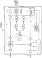
- FIG. 1 is a diagram illustrating a frequency modulation circuit of an FM-CW radar according to an embodiment of the present invention.
- An FM-CW radar 100-1 illustrated in FIG. 1 includes a frequency modulation circuit 110-1, a transmission antenna 1 connected to the frequency modulation circuit 110-1, and a reception antenna 14 connected to the frequency modulation circuit 110-1.
- the frequency modulation circuit 110-1 includes: a high-frequency circuit 2 connected to the transmission antenna 1 and the reception antenna 14; and a signal processing circuit 6 that generates a triangular wave voltage signal, which is a modulation control voltage based on a modulated signal to be output from the high-frequency circuit 2, and outputs the triangular wave voltage signal to a VCO 5 of the high-frequency circuit 2.
- the frequency modulation circuit 110-1 includes a single-phase differential converter 18, a baseband amplifier circuit 11, a Low Pass Filter (LPF) 24, an LPF 25, a control circuit 15, and an ambient temperature monitor 23.
- LPF Low Pass Filter
- the high-frequency circuit 2 includes: the VCO 5 that generates an oscillation frequency signal, which is a modulated signal subjected to frequency modulation in accordance with a frequency control voltage transmitted from the signal processing circuit 6; and a power distributor 4 that outputs most of an output of the VCO 5 to an amplifier 3 and outputs the remaining output to a mixer (MIX) 12, which is a frequency converter, as a local signal.
- a mixer MIX
- the high-frequency circuit 2 includes: an amplifier 3 that amplifies an output of the power distributor 4 and outputs the output to the transmission antenna 1; a low-noise amplifier 13 that amplifies a reception signal received by the reception antenna 14; and the MIX 12 that down-converts, with a local signal, the signal amplified by the low-noise amplifier 13 into an IF signal and outputs the IF signal.
- the high-frequency circuit 2 includes: a DIV 19 that performs frequency division of the oscillation frequency signal of the VCO 5 and outputs the oscillation frequency signal; a reference frequency generator 21 that outputs a local signal; and a MIX 20 that mixes the frequency division signal output from the DIV 19 and the local signal output from the reference frequency generator 21, down-converts, with the local signal, the frequency division signal into an IF signal and outputs the IF signal.
- a frequency of the IF signal is equivalent to a frequency of a difference between a frequency of the frequency division signal and a frequency of the local signal.
- the elements of the high-frequency circuit 2 are configured by Microwave Monolithic ICs (MMICs).
- MMICs Microwave Monolithic ICs
- the single-phase differential converter 18 converts a single-phase IF signal, that is, a single-end signal output from the MIX 20 into differential signals and outputs the differential signals.
- the LPF 25 reduces unnecessary waves and noise of a positive phase-side differential signal output from the single-phase differential converter 18 and outputs the positive phase-side differential signal.
- the LPF 24 reduces unnecessary waves and noise of an opposite phase-side differential signal output from the single-phase differential converter 18 and outputs the opposite phase-side differential signal.
- the baseband amplifier circuit 11 amplifies the output signal of the MIX 12 and outputs the amplified signal as a reception signal.
- the output signal of the LPF 24 is input to an ADC 16 in the signal processing circuit 6.
- the output signal of the LPF 25 is input to an ADC 17 in the signal processing circuit 6.
- the output signals are used for update of data for a triangular wave voltage signal in a LUT 22.
- the signal processing circuit 6 includes: a microcomputer 10, which is a main circuit unit that mainly performs transmission processing and measurement processing; and a Digital to Analog Converter (DAC) 7, which is a digital-analog converter that converts a triangular wave voltage signal transmitted from the microcomputer 10 into an analog signal and outputs the analog signal to the VCO 5 of the high-frequency circuit 2.
- DAC Digital to Analog Converter
- the signal processing circuit 6 includes: the ADC 16 that converts the output signal of the LPF 24 into a digital signal; the ADC 17 that converts the output signal of the LPF 25 into a digital signal; and an ADC 9 that converts the reception signal output from the baseband amplifier circuit 11 into a digital signal and outputs the digital signal to the microcomputer 10.
- the microcomputer 10 includes the LUT 22 that stores data for a triangular wave voltage signal given to the VCO 5 and a nonvolatile memory 8.
- An ambient temperature monitor 23 that measures an ambient temperature of the microcomputer 10 is connected to the microcomputer 10.
- the control circuit 15 controls, with the microcomputer 10, various control voltages supplied to the MMICs in the high-frequency circuit 2.
- the MMICs in the high-frequency circuit 2 have variations depending on manufacturing lots. Therefore, control voltage values adjusted and determined for each of the MMICs are stored in the nonvolatile memory in the microcomputer 10.
- the microcomputer 10 reads out the control voltage values from the nonvolatile memory 8 and supplies the control voltage values to the MMICs in the high-frequency circuit 2 via the control circuit 15.
- the VCO 5 generates, on the basis of the triangular wave voltage signal output from the signal processing circuit 6, an FM-CW signal, which is an oscillation frequency signal of high-frequency that includes a rising modulated signal, a frequency of which rises in a fixed period, and a falling modulated signal, a frequency of which falls in the fixed period.
- the FM-CW signal is input to the power distributor 4. Most of the FM-CW signal is supplied to the transmission antenna 1. A millimeter-wave radio wave is irradiated from the transmission antenna 1 toward a target object. The remaining FM-CW signal is supplied to the MIX 12 as a local signal.
- a reflected wave reflected on the target object is captured by the reception antenna 14 and input to the MIX 12 as a reception signal.
- the MIX 12 mixes the reception signal input from the reception antenna 14 and the local signal supplied from the power distributor 4, and outputs a beat signal having a frequency equivalent to a frequency difference between the signals.
- the beat signal is amplified to an appropriate level by the baseband amplifier circuit 11 and input to the microcomputer 10 via the ADC 9.
- the microcomputer 10 includes a signal processing unit 10-1 that calculates a distance to the target object and relative speed from a frequency in a rising modulation period and a frequency in a falling modulation period in the input beat signal, and outputs relative distance information on the distance to the target object and information on the relative speed with respect to the target object.
- these kinds of information output from the signal processing unit 10-1 are transmitted to a vehicle control unit 200 provided in a vehicle mounted with the FM-CW radar 100-1.
- the vehicle control unit 200 has a function of collectively controlling the operation of the vehicle mounted with the FM-CW radar 100-1.
- the vehicle control unit 200 performs, based on these kinds of information, processing such as clutter removal and target identification.
- the frequency of the FM-CW signal from the VCO 5 is reduced to a frequency of one fraction of an integer by the DIV 19 and input to the MIX 20.
- the frequency division signal output from the DIV 19 and the local signal output from the reference frequency generator 21 are mixed and an IF signal is output.
- the IF signal is converted into differential signals by the single-phase differential converter 18. After unnecessary waves and noise are removed from the differential signals by the LPF 24 and the LPF 25, the differential signals are input to the microcomputer 10 via the ADC 16 and the ADC 17.
- the microcomputer 10 measures, according to the quadrature demodulation scheme, a frequency from phase information of the IF signal, performs correction processing using a result of the measurement, calculates a voltage table necessary for securing modulation linearity of the frequency of the oscillation frequency signal, and updates the LUT 22 for a control voltage. Consequently, data for a triangular wave voltage signal output in the next cycle to the VCO 5 is updated.
- the updated data for the triangular wave voltage signal is converted into an analog signal, which is modulation control time-dependent voltage data, and input to the VCO 5 by the DAC 7.
- predetermined default chirp data is stored in the microcomputer 10 and the default chirp data is not output until the LUT 22 is updated after a frequency is measured.
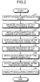
- FIG. 2 is a flowchart illustrating a modulation correcting operation in the microcomputer illustrated in FIG. 1 .
- FIG. 3 is a timing chart for explaining the modulation correcting operation in the microcomputer illustrated in FIG. 2 .
- a waveform of a modulation control voltage is illustrated on the upper side of FIG. 3 .
- a modulation frequency characteristic is illustrated on the lower side of FIG. 3 .
- Signs (1) to (8) illustrated in FIG. 3 correspond to numbers S1 to S8 illustrated in FIG. 2 .
- the microcomputer 10 outputs a modulation control voltage of default chirp, whereby the VCO 5 outputs a modulated signal of default chirp corresponding to the modulation control voltage (S1).
- the microcomputer 10 measures a frequency of a first-time VCO frequency division signal (S2).
- S2 voltage-frequency data corresponding to the default chip data is subjected to n-th order polynomial approximation (n is an integer equal to or larger than 2), for example, cubic function approximation.
- n-th order polynomial approximation n is an integer equal to or larger than 2
- a voltage table necessary for securing linearity is calculated from a result of the n-th order polynomial approximation. In this calculation, an inverse function thereof is used for correction and the modulation correction is performed (S3).
- the microcomputer 10 outputs a modulation control voltage after the inverse function correction, whereby the VCO 5 outputs a modulated signal corresponding to the modulation control voltage (S4).
- the microcomputer 10 measures frequencies of second and subsequent-time VCO frequency division signals (S5).
- the microcomputer 10 subjects time-frequency data to the n-th order polynomial approximation, for example, the cubic function approximation.
- the microcomputer 10 calculates a time error with respect to an ideal frequency straight line and performs correction of time data. In this calculation, the time error is used for correction and the modulation correction is performed (S6).
- the microcomputer 10 outputs a modulation control voltage after the time error correction, whereby the VCO 5 outputs a modulated signal corresponding to the modulation control voltage (S7).
- the modulation correction is completed (S8).
- the modulation frequency is corrected to a waveform illustrated in (8) in FIG. 3 by the operation in S1 to S8.
- FIG. 4 is a diagram illustrating a configuration for measuring a frequency from phase information in accordance with a quadrature demodulation scheme using an IF signal input to the signal processing circuit illustrated in FIG. 1 .
- the ADC 16 and the ADC 17 are equivalent to the ADC 16 and the ADC 17 illustrated in FIG. 1 , respectively.
- the microcomputer 10 After the IF signal is digitized, the microcomputer 10 performs differential arithmetic processing to calculate V'.
- the microcomputer 10 includes an LPF 10-2, an MIX 10-3, a frequency generating unit 10-4, a MIX 10-5, an LPF 10-6, an LPF 10-7, an instantaneous-phase-difference calculating unit 10-8, an instantaneous-frequency calculating unit 10-9, and a multiplying unit 10-10.
- Quadrature demodulation processing is performed by the MIX 10-3, the frequency generating unit 10-4, the MIX 10-5, and the multiplying unit 10-10.
- data sampled by the ADC 16 is separated into two signals of an I (In-phase) component and a Q (Quadrature) component according to quadrature detection.
- the LPF 10-2 in a first stage reduction processing for high-frequency and unnecessary wave components of the digitized IF signal is performed.
- the multiplying unit 10-10 performs the quadrature detection to thereby separate the IF signal into two signals of an I (In-phase) signal and a Q (Quadrature) signal
- the LPFs 10-6 and 10-7 in a second stage reduce a sum frequency component (f IF +f LO ) generated by multiplication processing and allow only a difference frequency component (f IF -f LO ) to pass.
- ⁇ t represents a time step.
- FIG. 5 is a diagram for explaining a time calculating method in the signal processing circuit illustrated in FIG. 1 .
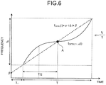
- FIG. 6 is a diagram for explaining an ideal-frequency-curve calculating method in the signal processing circuit illustrated in FIG. 1 .
- the horizontal axis indicates time and the vertical axis indicates a frequency.
- an opposite phase-side differential signal V + output from the single-phase differential converter 18 is input to the ADC 16 and a positive phase-side differential signal V - is input to the ADC 17.
- Each of the opposite phase-side differential signal V + and the positive phase-side differential signal V - is digitized. Thereafter, differential arithmetic processing is performed by a program of the microcomputer 10. Then, a frequency of the IF signal is measured from phase information according to the quadrature demodulation scheme. Note that, in S2, the same frequency measurement is performed.
- the time-frequency data measured in S5 is represented as f DETECT1 (t) .
- the time-frequency data f DETECT1 (t) is subjected to the n-th order polynomial approximation in a relation between time and a frequency.
- Frequency measurement data f DETECT1,A (t) after polynomial approximation is indicated by Expression (1) described below.
- Expression (1) described below is expanded to i-th discrete data, Expression (2) described below is obtained.
- a n , a n-1 , , and a 0 represent coefficients and ⁇ t represents a time step.
- a time error ⁇ t(t) is calculated from Expression (3) described below.
- Expression (3) described below is expanded to i-th discrete data, ⁇ t(i) indicated by Expression (4) below is obtained.
- ⁇ t t f DETECT 1 , A t ⁇ f IDEAL t ⁇ ′ t
- ⁇ t i f DETECT 1 , A i ⁇ f IDEAL i ⁇ ′ i
- ⁇ ' (t) represents a modulation gradient and is calculated by differentiating f DETECT1,A once.
- the modulation gradient a'(t) is indicated by Expression (5) described below.
- f IDEAL (t) represents an ideal frequency curve and is as indicated by Expression (7) described below.
- Expression (8) described below is obtained.
- ⁇ represents a modulation gradient theoretical value.
- F IDEAL at an A point (T 1 +T/2) illustrated in FIG. 6 is calculated by Expression (9) described below.
- a relation of Expression (10) described below holds from a condition that f DETECT1,A and f IDEAL are equal at the A point (T 1 +T/2). From Expression (10) described below, ⁇ indicated by Expression (11) described blow is calculated. [Math.
- the microcomputer 10 calculates any i-th time error ⁇ t(i) from Expression (2), Expression (8), and Expression (11) described above and additionally corrects the LUT 22 after the inverse function correction using the calculated time error ⁇ t(i) to obtain high modulation linearity as illustrated in (7) in FIG. 3 .
- FIG. 7 is a diagram illustrating a comparative example compared with the FM-CW radar according to the embodiment of the present invention.
- An FM-CW radar 100 illustrated in FIG. 7 is different in the following points compared with the FM-CW radar 100-1 in the embodiment.
- the microcomputer 10 illustrated in FIG. 7 measures an instantaneous frequency from instantaneous phase information on the IF signal, in accordance with the quadrature demodulation scheme using the signal converted into the digital signal by the ADC 16.
- the microcomputer 10 calculates an oscillation frequency of the VCO 5 from a frequency and a frequency division number of a local signal source. Time-frequency data measured in the quadrature demodulation scheme is poor in measurement accuracy. High linearity of frequency modulation cannot be obtained by performing feedback-control on the time-frequency data.
- the FM-CW radar 100-1 measures a frequency from phase information obtained by program execution processing of the microcomputer 10, performs n-th order polynomial (n is an integer equal to or larger than 2) approximation on time-frequency data of the IF signal output based on a modulation control voltage of chirp after inverse function correction, and performs modulation correction for correcting a time error. Consequently, effects explained below can be obtained.
- a DC offset, an even order harmonic, and common mode noise included in a signal can be reduced by converting an IF signal of a frequency division that is an output of a VCO into a differential output and performing the differential arithmetic processing with the differential arithmetic processing program of the microcomputer 10.
- a measurement error during frequency measurement in the quadrature demodulation scheme can be improved.
- a differential ADC is used as the ADC 16 illustrated in FIG. 7 , not only component cost but also an occupied area of a module configuring the differential ADC increases.
- the ADCs 16 and 17 corresponding to only a single end can be used. It is possible to reduce component cost and perform highly accurate frequency measurement.
- Modulation correction accuracy is improved by performing the highly accurate frequency measurement. As a result, the modulation linearity is improved. The distance to the target object and the relative speed can be more accurately calculated.
- a modulation band of the VCO 5 is wide. Even after down-conversion into an IF signal, in a low frequency range of the modulation band, in particular, a secondary harmonic component affects the modulation band. It is difficult to suppress the secondary harmonic component with the LPF 26 configured by hardware. However, by performing the differential arithmetic processing, the secondary harmonic component in the low frequency range of the modulation band can be reduced.
- an instantaneous frequency f of the IF signal is measured.
- the instantaneous frequency f of the IF signal is a frequency measured by the instantaneous-frequency calculating unit 10-9 explained above.
- a reception beat signal down-converted by the MIX 12 is converted into a digital signal by the ADC 9.
- the reception beat signal converted into the digital signal is subjected to Fast Fourier Transform (FFT) processing and signal processing.
- FFT Fast Fourier Transform
- a distance to the target object and relative speed are calculated.
- modulation correction accuracy is improved, the modulation linearity changes to a favorable characteristic, and calculation accuracy of a distance to the target object and relative speed by the FM-CW radar 100-1 is improved.
- the measurement error at the frequency measurement can be absorbed by approximating the measurement error with the n-th order polynomial as in Expression (1) described above. Highly accurate modulation correction is enabled by the absorption of the measurement error.
- a measurement error of a frequency is instantaneously caused by occurrence of vibration, noise, and electromagnetic noise, which are disturbances.
- the measurement error of the frequency cannot be absorbed.
- the instantaneously caused measurement error of the frequency can be absorbed by the n-th order polynomial approximation.
- FIG. 8 is a diagram illustrating a first modification of the FM-CW radar according to the embodiment of the present invention.
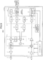
- a frequency modulation circuit 110-2 of an FM-CW radar 100-2 illustrated in FIG. 8 the reference frequency generator 21 and the MIX 20 illustrated in FIG. 1 are omitted.
- the frequency modulation circuit 110-2 includes the DIV 19 that performs frequency division of an oscillation frequency signal of the VCO 5 and outputs the oscillation frequency signal, and the single-phase differential converter 18 that converts a frequency division signal output from the DIV 19 into differential signals and outputs the differential signals.
- One of the differential signals is input to the LPF 24 and the other of the differential signals is input to the LPF 25.
- the microcomputer 10 of the signal processing circuit 6 illustrated in FIG. 8 measures a frequency from phase information of differential signals according to the quadrature demodulation scheme, performs n-th order polynomial (n is an integer equal to or larger than 2) approximation on differential signals output based on a modulation control voltage of default chirp, and performs modulation correction for correcting a time error of the differential signals.
- the reference frequency generator 21 and the MIX 20 illustrated in FIG. 1 are unnecessary.
- the configuration of the frequency modulation circuit 110-2 is simplified, manufacturing cost can be reduced, and reliability is improved.
- FIG. 9 is a diagram illustrating a second modification of the FM-CW radar according to the embodiment of the present invention.
- the single-phase differential converter 18 is omitted.
- the frequency-modulation circuit 110-3 includes the DIV 19 and the MIX 20 that down-converts a frequency division signal output from the DIV 19 and converts a single-phase IF signal into differential signals and outputs the differential signals.
- One of the differential signals is input to the LPF 24 and the other of the differential signals is input to the LPF 25.
- the microcomputer 10 of the signal processing circuit 6 illustrated in FIG. 9 measures a frequency from phase information of the IF signal in accordance with the quadrature demodulation scheme, performs n-th order polynomial (n is an integer equal to or larger than 2) approximation on the IF signal output based on a modulation control voltage of default chirp, and performs modulation correction for correcting a time difference of the IF signal.
- the single-phase differential converter 18 illustrated in FIG. 1 is unnecessary.
- the configuration of the frequency modulation circuit 110-3 is simplified, manufacturing cost can be reduced, and reliability is improved.
- FIG. 10 is a diagram illustrating a third modification of the FM-CW radar according to the embodiment of the present invention.
- a frequency modulation circuit 110-4 of an FM-CW radar 100-4 illustrated in FIG. 10 the MIX 20 and the reference frequency generator 21 illustrated in FIG. 1 are omitted.
- the frequency modulation circuit 110-4 includes a Balance unbalanced (Balun) 27, which is a balance-unbalance converter, instead of the single-phase differential converter 18 illustrated in FIG. 1 .
- the Balun 27 converts a single-end frequency division signal output from the DIV 19 into differential signals of a differential type and outputs the differential signals. One of the differential signals is input to the LPF 24 and the other of the differential signals is input to the LPF 25.
- the microcomputer 10 of the signal processing circuit 6 illustrated in FIG. 10 measures a frequency from phase information of the differential signals according to the quadrature demodulation scheme, performs n-th order polynomial (n is an integer equal to or larger than 2) approximation on the differential signals output based on a modulation control voltage of default chirp, and performs modulation correction for correcting a time difference of the differential signals.
- the reference frequency generator 21 and the MIX 20 illustrated in FIG. 1 are unnecessary.
- the configuration of the frequency modulation circuit 110-2 is simplified, manufacturing cost can be reduced, and reliability is improved.
- FIG. 11 is a diagram illustrating a fourth modulation of the FM-CW radar according to the embodiment of the present invention.
- a frequency modulation circuit 110-5 of an FM-CW radar 100-5 illustrated in FIG. 11 the MIX 20, the reference frequency generator 21, and the single-phase differential converter 18 illustrated in FIG. 1 are omitted.
- the DIV 19 of the frequency modulation circuit 110-5 performs frequency division of an oscillation frequency signal of the VCO 5 and converts a frequency division signal into differential signals and outputs the differential signals.
- One of the differential signals is input to the LPF 24 and the other of the differential signals is input to the LPF 25.
- the microcomputer 10 of the signal processing circuit 6 illustrated in FIG. 11 measures a frequency from phase information of the differential signals in accordance with the quadrature demodulation scheme, performs n-th order polynomial (n is an integer equal to or larger than 2) approximation on the differential signals output based on a modulation control voltage of default chirp, and corrects a time difference of the differential signals.
- the MIX 20, the reference frequency generator 21, and the single-phase differential converter 18 illustrated in FIG. 1 are unnecessary.
- the configuration of the frequency modulation circuit 110-5 is simplified, manufacturing cost can be reduced, and reliability is improved.
- FIG. 12 is a diagram illustrating a fifth modification of the FM-CW radar according to the embodiment of the present invention.
- a frequency modulation circuit 110-6 of an FM-CW radar 100-6 illustrated in FIG. 12 includes the Balun 27 instead of the single-phase differential converter 18 illustrated in FIG. 1 .
- the Balun 27 converts a single-phase IF signal output from the MIX 20 into differential signals and outputs the differential signals.
- One of the differential signals is input to the LPF 24 and the other of the differential signals is input to the LPF 25.
- the microcomputer 10 of the signal processing circuit 6 illustrated in FIG. 12 measures a frequency from phase information of the IF signal in accordance with the quadrature demodulation scheme, performs n-th order polynomial (n is an integer equal to or larger than 2) approximation on the differential signals output based on a modulation control voltage of default chirp, and performs modulation correction for correcting a time difference of the IF signal.
- the frequency modulation circuit according to this embodiment is provided in the FM-CW radar, which is an example of the radar that performs frequency modulation.
- the frequency modulation circuit according to this embodiment can be provided in a high-speed modulation radar.
- Both of the FM-CW radar and the high-speed modulation radar are radars that perform frequency modulation.
- the FM-CW radar is a radar that performs frequency modulation in a broad sense
- the high-speed modulation radar is a radar that performs frequency modulation in a narrow sense.
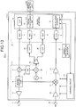
- FIG. 13 is a diagram illustrating a high-speed modulation radar according to the embodiment of the present invention.
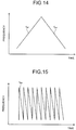
- FIG. 14 is a diagram representing frequency specification in the FM-CW radar according to the embodiment of the present invention.
- FIG. 15 is a diagram representing frequency specification in the high-speed modulation radar according to the embodiment of the present invention.
- a difference between the FM-CW radar 100-1 illustrated in FIG. 1 and a high-speed modulation radar 100-7 illustrated in FIG. 13 is that the arithmetic processing in the signal processing unit 10-1 is different.
- the high-speed modulation radar 100-7 illustrated in FIG. 13 includes the frequency modulation circuit 110-1 illustrated in FIG. 1 .
- the high-speed modulation radar 100-7 can include any one of the frequency modulation circuits 110-2 to 110-6 instead of the frequency modulation circuit 110-1.
- the same effects as the effects of the FM-CW radars 100-2 to 100-6 can be obtained.
- the arithmetic processing in the signal processing unit 10-1 provided in each of the FM-CW radars 100-1 to 100-6 and the high-speed modulation radar 100-7 is explained below.
- the vertical axis of FIG. 14 represents a frequency and the horizontal axis of FIG. 14 represents time.
- the signal processing unit 10-1 of the frequency conversion circuit provided in the FM-CW radars 100-1 to 100-6 selects a combination of an UP frequency f UP and a DOWN frequency f DN indicated by Expression (12) and Expression (13), respectively, described below and thereafter solves simultaneous equations to calculate a relative distance to the target object and relative speed.
- C represents high speed
- B represents a modulation bandwidth
- T represents a modulation time
- ⁇ represents a wavelength
- R represents a relative distance
- v relative speed.
- the vertical axis of FIG. 15 represents a frequency and the horizontal axis of FIG. 15 represents time.
- the signal processing unit 10-1 of the frequency modulation circuit provided in the high-speed modulation radar 100-7 calculates the relative distance R in accordance with Expression (14) described below.
- Expression (14) described below.
- the modulation time T is different.
- the modulation time T of the high-speed modulation radar 100-7 a time equal to or shorter than 1/100 of the modulation time T of the FM-CW radars 100-1 to 100-6 can be exemplary illustrated. Therefore, the FM-CW radars 100-1 to 100-6 can reduce sampling frequencies in the ADCs 16 and 17 compared with the high-speed modulation radar 100-7 and, therefore, can reduce power consumption.
- the high-speed modulation radar 100-7 has high modulation speed compared with the FM-CW radars 100-1 to 100-6.
- the high-speed modulation radar 100-7 can increase processing speed of processing such as clutter removal and target identification in the vehicle control unit 200.
- the FM-CW radars 100-1 to 100-6 has high linearity of frequency modulation. Therefore, the FM-CW radars 100-1 to 100-6 can more highly accurately calculate a relative distance to the target object and relative speed.
- the high-speed modulation radar 100-7 according to this embodiment has high linearity of frequency modulation. Therefore, the high-speed modulation radar 100-7 can more highly accurately calculate relative distance to the target object and relative speed. Further, the high-speed modulation radar 100-7 according to this embodiment has higher distinctiveness compared with the FM-CW radars 100-1 to 100-6. The high-speed modulation radar 100-7 can calculate an actual distance to the target object.
- the configuration explained above in the embodiment indicate an example of the content of the present invention.
- the configuration can be compared with other publicly-known technologies. A part of the configuration can be omitted or changed in a range not departing from the spirit of the present invention.
Landscapes
- Engineering & Computer Science (AREA)
- Radar, Positioning & Navigation (AREA)
- Remote Sensing (AREA)
- Computer Networks & Wireless Communication (AREA)
- Physics & Mathematics (AREA)
- General Physics & Mathematics (AREA)
- Signal Processing (AREA)
- Radar Systems Or Details Thereof (AREA)
Abstract
Description
- The present invention relates to a frequency modulation circuit of a radar that performs frequency modulation, an FM-CW radar, and a high-speed modulation radar.
- A conventional FM-CW radar adopting a Frequency Modulated-Continuous Waves (FM-CW) scheme, a circuit configuration of which is relatively simple, measures a frequency of a beat signal of a frequency-modulated transmission signal and a reception signal reflected from a target object, and calculates a relative distance and relative speed with respect to the target object. A Voltage Controlled Oscillator (VCO) is provided in the conventional FM-CW radar adopting the FM-CW scheme.
- The VCO outputs an oscillation frequency signal frequency-modulated according to a modulation control voltage. The oscillation frequency signal is requested to have high modulation linearity. However, because the VCO is a semiconductor device that controls a frequency with a voltage, the VCO shows a nonlinear frequency characteristic with respect to the voltage. The frequency characteristic of the VCO deviates according to individual variability or temperature characteristics. Therefore, in a shipment inspection process, work for measuring the oscillation frequency signal of the VCO and adjusting the oscillation frequency signal concerning modulation linearity is essential. The adjusting work is a hindrance to a reduction of an inspection time for mass production.
- To obtain the modulation linearity of the VCO, the conventional FM-CW radar represented by
Patent Literature 1 corrects the oscillation frequency signal of the VCO according to a Look Up Table (LUT) for modulation control voltage, or is provided with a mechanism for measuring the oscillation frequency signal of the VCO on a frequency modulation circuit to perform feedback control, to thereby cope with characteristic change of the VCO due to aged deterioration after shipment. - Patent Literature 1: Japanese Patent Application Laid-Open No.
2007-298317 - The conventional FM-CW radar represented by
Patent Literature 1 performs frequency division of the oscillation frequency signal of the VCO with a divider (DIV), which is a frequency divider, and thereafter converts an intermediate frequency (IF) signal, which is a signal having an intermediate frequency down-converted using a local signal, into a digital signal with an Analog to Digital Converter (ADC). Thereafter, the FM-CW radar measures an instantaneous frequency with a microcomputer from instantaneous phase information of the IF signal according to a quadrature demodulation scheme. - The oscillation frequency of the VCO is calculated from a frequency and a frequency division number of the local signal. However, there is a problem in that time-frequency data measured in the quadrature demodulation scheme is poor in measurement accuracy and high linearity of frequency modulation cannot be obtained even when the feedback control is performed.
- The present invention has been devised in view of the above, and an object of the present invention is to obtain a frequency modulation circuit that can obtain high linearity of frequency modulation.
- To solve the problem described above and achieve the object, a frequency modulation circuit of the present invention includes: a digital-analog converter to output modulation control time-dependent voltage data; a voltage control oscillator to oscillate, based on the modulation control time-dependent voltage data output from the digital-analog converter, an oscillation frequency signal; a frequency divider to perform frequency division of the oscillation frequency signal of the voltage control oscillator and output the oscillation frequency signal; a frequency converter to down-convert a frequency division signal output from the frequency divider; a single-phase differential converter to convert an intermediate frequency signal of single-phase output from the frequency converter into differential signals and output the differential signals; an analog-digital converter to convert, concerning the differential signals output from the single-phase differential converter, analog signals of the differential signals into digital signals; and a signal processing circuit to perform frequency measurement based on the differential signals of the analog-digital converter, update the modulation control time-dependent voltage data based on the measured frequency, and correct a time error of the oscillation frequency signal of the voltage control oscillator.
- According to the present invention, there is an effect that it is possible to obtain high linearity of frequency modulation.
-
-
FIG. 1 is a diagram illustrating a frequency modulation circuit of an FM-CW radar according to an embodiment of the present invention. -
FIG. 2 is a flowchart illustrating a modulation correcting operation in a microcomputer illustrated inFIG. 1 . -
FIG. 3 is a timing chart for explaining the modulation correcting operation in the microcomputer illustrated inFIG. 2 . -
FIG. 4 is a diagram illustrating a configuration for measuring a frequency from phase information according to a quadrature demodulation scheme using an IF signal input to a signal processing circuit illustrated inFIG. 1 . -
FIG. 5 is a diagram for explaining a time calculating method in the signal processing circuit illustrated inFIG. 1 . -
FIG. 6 is a diagram for explaining an ideal-frequency-curve calculating method in the signal processing circuit illustrated inFIG. 1 . -
FIG. 7 is a diagram illustrating a comparative example compared with the FM-CW radar according to the embodiment of the present invention. -
FIG. 8 is a diagram illustrating a first modification of the FM-CW radar according to the embodiment of the present invention. -
FIG. 9 is a diagram illustrating a second modification of the FM-CW radar according to the embodiment of the present invention. -
FIG. 10 is a diagram illustrating a third modification of the FM-CW radar according to the embodiment of the present invention. -
FIG. 11 is a diagram illustrating a fourth modification of the FM-CW radar according to the embodiment of the present invention. -
FIG. 12 is a diagram illustrating a fifth modification of the FM-CW radar according to the embodiment of the present invention. -
FIG. 13 is a diagram illustrating a high-speed modulation radar according to the embodiment of the present invention. -
FIG. 14 is a diagram representing frequency specification in the FM-CW radar according to the embodiment of the present invention. -
FIG. 15 is a diagram representing frequency specification in a high-speed modulation radar according to the embodiment of the present invention. - A frequency modulation circuit, an FM-CW radar, and a high-speed modulation radar according to an embodiment of the present invention are explained in detail below with reference to the drawings. Note that the present invention is not limited by this embodiment.
-
FIG. 1 is a diagram illustrating a frequency modulation circuit of an FM-CW radar according to an embodiment of the present invention. An FM-CW radar 100-1 illustrated inFIG. 1 includes a frequency modulation circuit 110-1, atransmission antenna 1 connected to the frequency modulation circuit 110-1, and areception antenna 14 connected to the frequency modulation circuit 110-1. - The frequency modulation circuit 110-1 includes: a high-
frequency circuit 2 connected to thetransmission antenna 1 and thereception antenna 14; and asignal processing circuit 6 that generates a triangular wave voltage signal, which is a modulation control voltage based on a modulated signal to be output from the high-frequency circuit 2, and outputs the triangular wave voltage signal to aVCO 5 of the high-frequency circuit 2. The frequency modulation circuit 110-1 includes a single-phasedifferential converter 18, abaseband amplifier circuit 11, a Low Pass Filter (LPF) 24, anLPF 25, acontrol circuit 15, and anambient temperature monitor 23. - The high-
frequency circuit 2 includes: theVCO 5 that generates an oscillation frequency signal, which is a modulated signal subjected to frequency modulation in accordance with a frequency control voltage transmitted from thesignal processing circuit 6; and apower distributor 4 that outputs most of an output of theVCO 5 to anamplifier 3 and outputs the remaining output to a mixer (MIX) 12, which is a frequency converter, as a local signal. - The high-
frequency circuit 2 includes: anamplifier 3 that amplifies an output of thepower distributor 4 and outputs the output to thetransmission antenna 1; a low-noise amplifier 13 that amplifies a reception signal received by thereception antenna 14; and theMIX 12 that down-converts, with a local signal, the signal amplified by the low-noise amplifier 13 into an IF signal and outputs the IF signal. - The high-
frequency circuit 2 includes: aDIV 19 that performs frequency division of the oscillation frequency signal of theVCO 5 and outputs the oscillation frequency signal; areference frequency generator 21 that outputs a local signal; and aMIX 20 that mixes the frequency division signal output from theDIV 19 and the local signal output from thereference frequency generator 21, down-converts, with the local signal, the frequency division signal into an IF signal and outputs the IF signal. A frequency of the IF signal is equivalent to a frequency of a difference between a frequency of the frequency division signal and a frequency of the local signal. - The elements of the high-
frequency circuit 2 are configured by Microwave Monolithic ICs (MMICs). - The single-phase
differential converter 18 converts a single-phase IF signal, that is, a single-end signal output from theMIX 20 into differential signals and outputs the differential signals. TheLPF 25 reduces unnecessary waves and noise of a positive phase-side differential signal output from the single-phasedifferential converter 18 and outputs the positive phase-side differential signal. TheLPF 24 reduces unnecessary waves and noise of an opposite phase-side differential signal output from the single-phasedifferential converter 18 and outputs the opposite phase-side differential signal. Thebaseband amplifier circuit 11 amplifies the output signal of theMIX 12 and outputs the amplified signal as a reception signal. - The output signal of the
LPF 24 is input to anADC 16 in thesignal processing circuit 6. The output signal of theLPF 25 is input to anADC 17 in thesignal processing circuit 6. The output signals are used for update of data for a triangular wave voltage signal in aLUT 22. - The
signal processing circuit 6 includes: amicrocomputer 10, which is a main circuit unit that mainly performs transmission processing and measurement processing; and a Digital to Analog Converter (DAC) 7, which is a digital-analog converter that converts a triangular wave voltage signal transmitted from themicrocomputer 10 into an analog signal and outputs the analog signal to theVCO 5 of the high-frequency circuit 2. - The
signal processing circuit 6 includes: theADC 16 that converts the output signal of theLPF 24 into a digital signal; theADC 17 that converts the output signal of theLPF 25 into a digital signal; and anADC 9 that converts the reception signal output from thebaseband amplifier circuit 11 into a digital signal and outputs the digital signal to themicrocomputer 10. - The
microcomputer 10 includes theLUT 22 that stores data for a triangular wave voltage signal given to theVCO 5 and anonvolatile memory 8. An ambient temperature monitor 23 that measures an ambient temperature of themicrocomputer 10 is connected to themicrocomputer 10. - The
control circuit 15 controls, with themicrocomputer 10, various control voltages supplied to the MMICs in the high-frequency circuit 2. Specifically, the MMICs in the high-frequency circuit 2 have variations depending on manufacturing lots. Therefore, control voltage values adjusted and determined for each of the MMICs are stored in the nonvolatile memory in themicrocomputer 10. During actual operation, themicrocomputer 10 reads out the control voltage values from thenonvolatile memory 8 and supplies the control voltage values to the MMICs in the high-frequency circuit 2 via thecontrol circuit 15. - The operation of the FM-CW radar 100-1 is explained below.
- The
VCO 5 generates, on the basis of the triangular wave voltage signal output from thesignal processing circuit 6, an FM-CW signal, which is an oscillation frequency signal of high-frequency that includes a rising modulated signal, a frequency of which rises in a fixed period, and a falling modulated signal, a frequency of which falls in the fixed period. - The FM-CW signal is input to the
power distributor 4. Most of the FM-CW signal is supplied to thetransmission antenna 1. A millimeter-wave radio wave is irradiated from thetransmission antenna 1 toward a target object. The remaining FM-CW signal is supplied to theMIX 12 as a local signal. - A reflected wave reflected on the target object is captured by the
reception antenna 14 and input to theMIX 12 as a reception signal. TheMIX 12 mixes the reception signal input from thereception antenna 14 and the local signal supplied from thepower distributor 4, and outputs a beat signal having a frequency equivalent to a frequency difference between the signals. The beat signal is amplified to an appropriate level by thebaseband amplifier circuit 11 and input to themicrocomputer 10 via theADC 9. - The
microcomputer 10 includes a signal processing unit 10-1 that calculates a distance to the target object and relative speed from a frequency in a rising modulation period and a frequency in a falling modulation period in the input beat signal, and outputs relative distance information on the distance to the target object and information on the relative speed with respect to the target object. Note that these kinds of information output from the signal processing unit 10-1 are transmitted to avehicle control unit 200 provided in a vehicle mounted with the FM-CW radar 100-1. Thevehicle control unit 200 has a function of collectively controlling the operation of the vehicle mounted with the FM-CW radar 100-1. Thevehicle control unit 200 performs, based on these kinds of information, processing such as clutter removal and target identification. - On the other hand, the frequency of the FM-CW signal from the
VCO 5 is reduced to a frequency of one fraction of an integer by theDIV 19 and input to theMIX 20. - In the
MIX 20, the frequency division signal output from theDIV 19 and the local signal output from thereference frequency generator 21 are mixed and an IF signal is output. - The IF signal is converted into differential signals by the single-
phase differential converter 18. After unnecessary waves and noise are removed from the differential signals by theLPF 24 and theLPF 25, the differential signals are input to themicrocomputer 10 via theADC 16 and theADC 17. - The
microcomputer 10 measures, according to the quadrature demodulation scheme, a frequency from phase information of the IF signal, performs correction processing using a result of the measurement, calculates a voltage table necessary for securing modulation linearity of the frequency of the oscillation frequency signal, and updates theLUT 22 for a control voltage. Consequently, data for a triangular wave voltage signal output in the next cycle to theVCO 5 is updated. The updated data for the triangular wave voltage signal is converted into an analog signal, which is modulation control time-dependent voltage data, and input to theVCO 5 by theDAC 7. - Note that, as for an initial value of modulation control data, predetermined default chirp data is stored in the
microcomputer 10 and the default chirp data is not output until theLUT 22 is updated after a frequency is measured. - Correction processing for obtaining modulation linearity of the
VCO 5 is explained. -
FIG. 2 is a flowchart illustrating a modulation correcting operation in the microcomputer illustrated inFIG. 1 .FIG. 3 is a timing chart for explaining the modulation correcting operation in the microcomputer illustrated inFIG. 2 . A waveform of a modulation control voltage is illustrated on the upper side ofFIG. 3 . A modulation frequency characteristic is illustrated on the lower side ofFIG. 3 . Signs (1) to (8) illustrated inFIG. 3 correspond to numbers S1 to S8 illustrated inFIG. 2 . - The
microcomputer 10 outputs a modulation control voltage of default chirp, whereby theVCO 5 outputs a modulated signal of default chirp corresponding to the modulation control voltage (S1). Themicrocomputer 10 measures a frequency of a first-time VCO frequency division signal (S2). When theLUT 22 is updated, voltage-frequency data corresponding to the default chip data is subjected to n-th order polynomial approximation (n is an integer equal to or larger than 2), for example, cubic function approximation. A voltage table necessary for securing linearity is calculated from a result of the n-th order polynomial approximation. In this calculation, an inverse function thereof is used for correction and the modulation correction is performed (S3). - The
microcomputer 10 outputs a modulation control voltage after the inverse function correction, whereby theVCO 5 outputs a modulated signal corresponding to the modulation control voltage (S4). Themicrocomputer 10 measures frequencies of second and subsequent-time VCO frequency division signals (S5). Themicrocomputer 10 subjects time-frequency data to the n-th order polynomial approximation, for example, the cubic function approximation. When theLUT 22 is updated for the second and subsequent times, themicrocomputer 10 calculates a time error with respect to an ideal frequency straight line and performs correction of time data. In this calculation, the time error is used for correction and the modulation correction is performed (S6). Themicrocomputer 10 outputs a modulation control voltage after the time error correction, whereby theVCO 5 outputs a modulated signal corresponding to the modulation control voltage (S7). The modulation correction is completed (S8). The modulation frequency is corrected to a waveform illustrated in (8) inFIG. 3 by the operation in S1 to S8. - A calculation method for an error time in S5 to S8 in
FIG. 2 is explained in detail.FIG. 4 is a diagram illustrating a configuration for measuring a frequency from phase information in accordance with a quadrature demodulation scheme using an IF signal input to the signal processing circuit illustrated inFIG. 1 . TheADC 16 and theADC 17 are equivalent to theADC 16 and theADC 17 illustrated inFIG. 1 , respectively. After the IF signal is digitized, themicrocomputer 10 performs differential arithmetic processing to calculate V'. Themicrocomputer 10 includes an LPF 10-2, an MIX 10-3, a frequency generating unit 10-4, a MIX 10-5, an LPF 10-6, an LPF 10-7, an instantaneous-phase-difference calculating unit 10-8, an instantaneous-frequency calculating unit 10-9, and a multiplying unit 10-10. Quadrature demodulation processing is performed by the MIX 10-3, the frequency generating unit 10-4, the MIX 10-5, and the multiplying unit 10-10. Specifically, data sampled by theADC 16 is separated into two signals of an I (In-phase) component and a Q (Quadrature) component according to quadrature detection. In the LPF 10-2 in a first stage, reduction processing for high-frequency and unnecessary wave components of the digitized IF signal is performed. After the multiplying unit 10-10 performs the quadrature detection to thereby separate the IF signal into two signals of an I (In-phase) signal and a Q (Quadrature) signal, the LPFs 10-6 and 10-7 in a second stage reduce a sum frequency component (fIF+fLO) generated by multiplication processing and allow only a difference frequency component (fIF-fLO) to pass. After an instantaneous phase difference Δθ=Tan-1(Q/I) of the IF signal is calculated from the I signal and the Q signal by the instantaneous-phase-difference calculating unit 10-8, an instantaneous frequency f=Δθ/Δt of the IF signal is calculated by the instantaneous-frequency calculating unit 10-9. Δt represents a time step. -
FIG. 5 is a diagram for explaining a time calculating method in the signal processing circuit illustrated inFIG. 1 .FIG. 6 is a diagram for explaining an ideal-frequency-curve calculating method in the signal processing circuit illustrated inFIG. 1 . In each ofFIG. 5 andFIG. 6 , the horizontal axis indicates time and the vertical axis indicates a frequency. - As illustrated in
FIG. 4 , an opposite phase-side differential signal V+ output from the single-phase differential converter 18 is input to theADC 16 and a positive phase-side differential signal V- is input to theADC 17. Each of the opposite phase-side differential signal V+ and the positive phase-side differential signal V- is digitized. Thereafter, differential arithmetic processing is performed by a program of themicrocomputer 10. Then, a frequency of the IF signal is measured from phase information according to the quadrature demodulation scheme. Note that, in S2, the same frequency measurement is performed. The time-frequency data measured in S5 is represented as fDETECT1(t) . - A method of calculating a time error with respect to an ideal frequency from fDETECT1(t) is explained below.
- The time-frequency data fDETECT1(t) is subjected to the n-th order polynomial approximation in a relation between time and a frequency. Frequency measurement data fDETECT1,A(t) after polynomial approximation is indicated by Expression (1) described below. When Expression (1) described below is expanded to i-th discrete data, Expression (2) described below is obtained. In the expressions, an, an-1, , and a0 (n is a natural number) represent coefficients and Δt represents a time step.
[Math. 1]
[Math. 2]
- A time error ∂t(t) is calculated from Expression (3) described below. When Expression (3) described below is expanded to i-th discrete data, ∂t(i) indicated by Expression (4) below is obtained.
[Math. 3]
[Math. 4]
- In Expression (3) described above, α' (t) represents a modulation gradient and is calculated by differentiating fDETECT1,A once. The modulation gradient a'(t) is indicated by Expression (5) described below. When Expression (4) described above is expanded to i-th discrete data, α' (i) indicated by Expression (6) described below is obtained.
[Math. 5]
[Math. 6]
- In Expression (3) described above, fIDEAL(t) represents an ideal frequency curve and is as indicated by Expression (7) described below. When Expression (7) described below is expanded to i-th discrete data, Expression (8) described below is obtained. In Expression (7) and Expression (8) described below, α represents a modulation gradient theoretical value.
[Math. 7]
[Math. 8]
- A calculation method for β in Expression (7) and Expression (8) described above is explained below. β is calculated by resetting fIDEAL(t) from a modulation center point T1+T/2 of a frequency measurement result fDETECT1,A to t=0. Specifically, FIDEAL at an A point (T1+T/2) illustrated in
FIG. 6 is calculated by Expression (9) described below. A relation of Expression (10) described below holds from a condition that fDETECT1,A and fIDEAL are equal at the A point (T1+T/2). From Expression (10) described below, β indicated by Expression (11) described blow is calculated.
[Math. 9]
[Math. 10]
[Math. 11]
- The
microcomputer 10 calculates any i-th time error ∂t(i) from Expression (2), Expression (8), and Expression (11) described above and additionally corrects theLUT 22 after the inverse function correction using the calculated time error ∂t(i) to obtain high modulation linearity as illustrated in (7) inFIG. 3 . -
FIG. 7 is a diagram illustrating a comparative example compared with the FM-CW radar according to the embodiment of the present invention. An FM-CW radar 100 illustrated inFIG. 7 is different in the following points compared with the FM-CW radar 100-1 in the embodiment. - (1) In a frequency modulation circuit 110 of the FM-
CW radar 100, a single-phase IF signal output from theMIX 20 is input to anLPF 26. - (2) An output signal of the
LPF 26 is input to theADC 16 in thesignal processing circuit 6 and converted into a digital signal. - The
microcomputer 10 illustrated inFIG. 7 measures an instantaneous frequency from instantaneous phase information on the IF signal, in accordance with the quadrature demodulation scheme using the signal converted into the digital signal by theADC 16. Themicrocomputer 10 calculates an oscillation frequency of theVCO 5 from a frequency and a frequency division number of a local signal source. Time-frequency data measured in the quadrature demodulation scheme is poor in measurement accuracy. High linearity of frequency modulation cannot be obtained by performing feedback-control on the time-frequency data. - After the
signal processing circuit 6 performs differential arithmetic processing of the IF signal with a differential arithmetic processing program in accordance with the quadrature demodulation scheme, the FM-CW radar 100-1 according to the embodiment of the present invention measures a frequency from phase information obtained by program execution processing of themicrocomputer 10, performs n-th order polynomial (n is an integer equal to or larger than 2) approximation on time-frequency data of the IF signal output based on a modulation control voltage of chirp after inverse function correction, and performs modulation correction for correcting a time error. Consequently, effects explained below can be obtained. - A DC offset, an even order harmonic, and common mode noise included in a signal can be reduced by converting an IF signal of a frequency division that is an output of a VCO into a differential output and performing the differential arithmetic processing with the differential arithmetic processing program of the
microcomputer 10. A measurement error during frequency measurement in the quadrature demodulation scheme can be improved. When a differential ADC is used as theADC 16 illustrated inFIG. 7 , not only component cost but also an occupied area of a module configuring the differential ADC increases. However, in the FM-CW radar 100-1 according to this embodiment, theADCs VCO 5 is wide. Even after down-conversion into an IF signal, in a low frequency range of the modulation band, in particular, a secondary harmonic component affects the modulation band. It is difficult to suppress the secondary harmonic component with theLPF 26 configured by hardware. However, by performing the differential arithmetic processing, the secondary harmonic component in the low frequency range of the modulation band can be reduced. - In the
microcomputer 10, based on a single-phase IF signal output from theMIX 20, an instantaneous frequency f of the IF signal is measured. The instantaneous frequency f of the IF signal is a frequency measured by the instantaneous-frequency calculating unit 10-9 explained above. Concerning a frequency-time waveform of a frequency in a rising modulation period of the IF signal and a frequency in a falling modulation period of the IF signal, themicrocomputer 10 performs the modulation correction explained with reference toFIG. 2 andFIG. 3 . After the FM-CW radar 100-1 transmits an FM-CW signal generated based on theLUT 22 after the modulation correction and receives a reflected wave from the target object, a reception beat signal down-converted by theMIX 12 is converted into a digital signal by theADC 9. The reception beat signal converted into the digital signal is subjected to Fast Fourier Transform (FFT) processing and signal processing. A distance to the target object and relative speed are calculated. As a result of the highly accurate frequency measurement of theVCO 5, modulation correction accuracy is improved, the modulation linearity changes to a favorable characteristic, and calculation accuracy of a distance to the target object and relative speed by the FM-CW radar 100-1 is improved. - When the frequency measurement is performed by the quadrature demodulation scheme, a measurement error is caused by noise, a DC offset, and a harmonic component included in the IF signal. Therefore, when a time difference is calculated based on time-frequency data including the measurement error and time error correction is performed, it is difficult to obtain high modulation linearity with the highly accurate modulation correction. According to this embodiment, the measurement error at the frequency measurement can be absorbed by approximating the measurement error with the n-th order polynomial as in Expression (1) described above. Highly accurate modulation correction is enabled by the absorption of the measurement error. In a module of a general FM-CW radar, it can be predicted that a measurement error of a frequency is instantaneously caused by occurrence of vibration, noise, and electromagnetic noise, which are disturbances. However, the measurement error of the frequency cannot be absorbed. According to this embodiment, the instantaneously caused measurement error of the frequency can be absorbed by the n-th order polynomial approximation.
- On the other hand, in the
VCO 5, a certain fixed error is caused in frequency measurement due to a temperature drift according to a physical property of a semiconductor. Therefore, when an intercept β in Expression (7) and Expression (8) described above of an ideal frequency curve is fixed at a theoretical value like the gradient α that is fixed, a correction amount becomes excessive. Accurate modulation correction sometimes cannot be performed in such a case. Therefore, in this embodiment, by using Expression (11) described above, it is possible to prevent the correction amount from becoming excessive. Thus, stable modulation correction is enabled. -
FIG. 8 is a diagram illustrating a first modification of the FM-CW radar according to the embodiment of the present invention. In a frequency modulation circuit 110-2 of an FM-CW radar 100-2 illustrated inFIG. 8 , thereference frequency generator 21 and theMIX 20 illustrated inFIG. 1 are omitted. - The frequency modulation circuit 110-2 includes the
DIV 19 that performs frequency division of an oscillation frequency signal of theVCO 5 and outputs the oscillation frequency signal, and the single-phase differential converter 18 that converts a frequency division signal output from theDIV 19 into differential signals and outputs the differential signals. One of the differential signals is input to theLPF 24 and the other of the differential signals is input to theLPF 25. - The
microcomputer 10 of thesignal processing circuit 6 illustrated inFIG. 8 measures a frequency from phase information of differential signals according to the quadrature demodulation scheme, performs n-th order polynomial (n is an integer equal to or larger than 2) approximation on differential signals output based on a modulation control voltage of default chirp, and performs modulation correction for correcting a time error of the differential signals. - With the frequency modulation circuit 110-2, the
reference frequency generator 21 and theMIX 20 illustrated inFIG. 1 are unnecessary. The configuration of the frequency modulation circuit 110-2 is simplified, manufacturing cost can be reduced, and reliability is improved. -
FIG. 9 is a diagram illustrating a second modification of the FM-CW radar according to the embodiment of the present invention. In a frequency modulation circuit 110-3 of an FM-CW radar 100-3 illustrated inFIG. 9 , the single-phase differential converter 18 is omitted. - The frequency-modulation circuit 110-3 includes the
DIV 19 and theMIX 20 that down-converts a frequency division signal output from theDIV 19 and converts a single-phase IF signal into differential signals and outputs the differential signals. One of the differential signals is input to theLPF 24 and the other of the differential signals is input to theLPF 25. - The
microcomputer 10 of thesignal processing circuit 6 illustrated inFIG. 9 measures a frequency from phase information of the IF signal in accordance with the quadrature demodulation scheme, performs n-th order polynomial (n is an integer equal to or larger than 2) approximation on the IF signal output based on a modulation control voltage of default chirp, and performs modulation correction for correcting a time difference of the IF signal. - With the frequency modulation circuit 110-3, the single-
phase differential converter 18 illustrated inFIG. 1 is unnecessary. The configuration of the frequency modulation circuit 110-3 is simplified, manufacturing cost can be reduced, and reliability is improved. -
FIG. 10 is a diagram illustrating a third modification of the FM-CW radar according to the embodiment of the present invention. In a frequency modulation circuit 110-4 of an FM-CW radar 100-4 illustrated inFIG. 10 , theMIX 20 and thereference frequency generator 21 illustrated inFIG. 1 are omitted. - The frequency modulation circuit 110-4 includes a Balance unbalanced (Balun) 27, which is a balance-unbalance converter, instead of the single-
phase differential converter 18 illustrated inFIG. 1 . TheBalun 27 converts a single-end frequency division signal output from theDIV 19 into differential signals of a differential type and outputs the differential signals. One of the differential signals is input to theLPF 24 and the other of the differential signals is input to theLPF 25. - The
microcomputer 10 of thesignal processing circuit 6 illustrated inFIG. 10 measures a frequency from phase information of the differential signals according to the quadrature demodulation scheme, performs n-th order polynomial (n is an integer equal to or larger than 2) approximation on the differential signals output based on a modulation control voltage of default chirp, and performs modulation correction for correcting a time difference of the differential signals. - With the frequency modulation circuit 110-4, the
reference frequency generator 21 and theMIX 20 illustrated inFIG. 1 are unnecessary. The configuration of the frequency modulation circuit 110-2 is simplified, manufacturing cost can be reduced, and reliability is improved. -
FIG. 11 is a diagram illustrating a fourth modulation of the FM-CW radar according to the embodiment of the present invention. In a frequency modulation circuit 110-5 of an FM-CW radar 100-5 illustrated inFIG. 11 , theMIX 20, thereference frequency generator 21, and the single-phase differential converter 18 illustrated inFIG. 1 are omitted. - The
DIV 19 of the frequency modulation circuit 110-5 performs frequency division of an oscillation frequency signal of theVCO 5 and converts a frequency division signal into differential signals and outputs the differential signals. One of the differential signals is input to theLPF 24 and the other of the differential signals is input to theLPF 25. - The
microcomputer 10 of thesignal processing circuit 6 illustrated inFIG. 11 measures a frequency from phase information of the differential signals in accordance with the quadrature demodulation scheme, performs n-th order polynomial (n is an integer equal to or larger than 2) approximation on the differential signals output based on a modulation control voltage of default chirp, and corrects a time difference of the differential signals. - With the frequency modulation circuit 110-5, the
MIX 20, thereference frequency generator 21, and the single-phase differential converter 18 illustrated inFIG. 1 are unnecessary. The configuration of the frequency modulation circuit 110-5 is simplified, manufacturing cost can be reduced, and reliability is improved. -
FIG. 12 is a diagram illustrating a fifth modification of the FM-CW radar according to the embodiment of the present invention. A frequency modulation circuit 110-6 of an FM-CW radar 100-6 illustrated inFIG. 12 includes theBalun 27 instead of the single-phase differential converter 18 illustrated inFIG. 1 . - The
Balun 27 converts a single-phase IF signal output from theMIX 20 into differential signals and outputs the differential signals. One of the differential signals is input to theLPF 24 and the other of the differential signals is input to theLPF 25. - The
microcomputer 10 of thesignal processing circuit 6 illustrated inFIG. 12 measures a frequency from phase information of the IF signal in accordance with the quadrature demodulation scheme, performs n-th order polynomial (n is an integer equal to or larger than 2) approximation on the differential signals output based on a modulation control voltage of default chirp, and performs modulation correction for correcting a time difference of the IF signal. - With the frequency modulation circuit 110-6, it is unnecessary to use the differential ADC and an increase in an occupied area can be reduced as in the frequency modulation circuit 110-1 illustrated in
FIG. 1 . - The example is explained above in which the frequency modulation circuit according to this embodiment is provided in the FM-CW radar, which is an example of the radar that performs frequency modulation. However, the frequency modulation circuit according to this embodiment can be provided in a high-speed modulation radar. Both of the FM-CW radar and the high-speed modulation radar are radars that perform frequency modulation. However, the FM-CW radar is a radar that performs frequency modulation in a broad sense and the high-speed modulation radar is a radar that performs frequency modulation in a narrow sense.
FIG. 13 is a diagram illustrating a high-speed modulation radar according to the embodiment of the present invention.FIG. 14 is a diagram representing frequency specification in the FM-CW radar according to the embodiment of the present invention.FIG. 15 is a diagram representing frequency specification in the high-speed modulation radar according to the embodiment of the present invention. - A difference between the FM-CW radar 100-1 illustrated in
FIG. 1 and a high-speed modulation radar 100-7 illustrated inFIG. 13 is that the arithmetic processing in the signal processing unit 10-1 is different. The high-speed modulation radar 100-7 illustrated inFIG. 13 includes the frequency modulation circuit 110-1 illustrated inFIG. 1 . However, the high-speed modulation radar 100-7 can include any one of the frequency modulation circuits 110-2 to 110-6 instead of the frequency modulation circuit 110-1. By including any one of the frequency modulation circuits 110-2 to 110-6, the same effects as the effects of the FM-CW radars 100-2 to 100-6 can be obtained. The arithmetic processing in the signal processing unit 10-1 provided in each of the FM-CW radars 100-1 to 100-6 and the high-speed modulation radar 100-7 is explained below. - The vertical axis of
FIG. 14 represents a frequency and the horizontal axis ofFIG. 14 represents time. The signal processing unit 10-1 of the frequency conversion circuit provided in the FM-CW radars 100-1 to 100-6 selects a combination of an UP frequency fUP and a DOWN frequency fDN indicated by Expression (12) and Expression (13), respectively, described below and thereafter solves simultaneous equations to calculate a relative distance to the target object and relative speed. Note that, in Expression (12) and Expression (13) described below, C represents high speed, B represents a modulation bandwidth, T represents a modulation time, λ represents a wavelength, R represents a relative distance, and v represents relative speed.
[Math. 12]
[Math. 13]
- The vertical axis of
FIG. 15 represents a frequency and the horizontal axis ofFIG. 15 represents time. The signal processing unit 10-1 of the frequency modulation circuit provided in the high-speed modulation radar 100-7 calculates the relative distance R in accordance with Expression (14) described below. In the high-speed modulation radar 100-7, because chirp speed is high compared with the FM-CW radars 100-1 to 100-6, the item of the relative speed v can be neglected compared with the relative distance R. Therefore, 2v/λ can be regarded as 0. After collecting data for each distance bin, the signal processing unit 10-1 performs doppler processing to calculate the relative speed v.
[Math. 14]
- In the high-speed modulation radar 100-7, compared with the FM-CW radars 100-1 to 100-6, the modulation time T is different. As the modulation time T of the high-speed modulation radar 100-7, a time equal to or shorter than 1/100 of the modulation time T of the FM-CW radars 100-1 to 100-6 can be exemplary illustrated. Therefore, the FM-CW radars 100-1 to 100-6 can reduce sampling frequencies in the
ADCs vehicle control unit 200. - The FM-CW radars 100-1 to 100-6 according to this embodiment has high linearity of frequency modulation. Therefore, the FM-CW radars 100-1 to 100-6 can more highly accurately calculate a relative distance to the target object and relative speed. The high-speed modulation radar 100-7 according to this embodiment has high linearity of frequency modulation. Therefore, the high-speed modulation radar 100-7 can more highly accurately calculate relative distance to the target object and relative speed. Further, the high-speed modulation radar 100-7 according to this embodiment has higher distinctiveness compared with the FM-CW radars 100-1 to 100-6. The high-speed modulation radar 100-7 can calculate an actual distance to the target object.
- The configuration explained above in the embodiment indicate an example of the content of the present invention. The configuration can be compared with other publicly-known technologies. A part of the configuration can be omitted or changed in a range not departing from the spirit of the present invention.
- 1 transmission antenna; 2 high-frequency circuit; 3 amplifier; 4 power distributor; 5 VCO; 6 signal processing circuit; 7 DAC; 8 nonvolatile memory; 9, 16, 17 ADC; 10 microcomputer; 10-1 signal processing unit; 10-2, 10-6, 10-7 LPF; 10-3, 10-5, 12, 20 MIX; 10-4 frequency generating unit; 10-8 instantaneous-phase-difference calculating unit; 10-9 instantaneous-frequency calculating unit; 10-10 multiplying unit; 11 baseband amplifier circuit; 13 low-noise amplifier; 14 reception antenna; 15 control circuit; 18 single-phase differential converter; 19 DIV; 21 reference frequency generator; 22 LUT; 23 ambient temperature monitor; 24, 25, 26 LPF; 27 Balun; 100, 100-1, 100-2, 100-3, 100-4, 100-5, 100-6 FM-CW radar; 110, 110-1, 110-2, 110-3, 110-4, 110-5, 110-6 frequency modulation circuit; 100-7 high-speed modulation radar; 200 vehicle control unit.
Claims (11)
- A frequency modulation circuit comprising:a digital-analog converter to output modulation control time-dependent voltage data;a voltage control oscillator to oscillate, based on the modulation control time-dependent voltage data output from the digital-analog converter, an oscillation frequency signal;a frequency divider to perform frequency division of the oscillation frequency signal of the voltage control oscillator and output the oscillation frequency signal;a frequency converter to down-convert a frequency division signal output from the frequency divider;a single-phase differential converter to convert an intermediate frequency signal of single-phase output from the frequency converter into differential signals and output the differential signals;an analog-digital converter to convert, concerning the differential signals output from the single-phase differential converter, analog signals of the differential signals into digital signals; anda signal processing circuit to perform frequency measurement based on the differential signals of the analog-digital converter, update the modulation control time-dependent voltage data based on the measured frequency, and correct a time error of the oscillation frequency signal of the voltage control oscillator.
- A frequency modulation circuit comprising:a digital-analog converter to output modulation control time-dependent voltage data;a voltage control oscillator to oscillate, based on the modulation control time-dependent voltage data output from the digital-analog converter, an oscillation frequency signal;a frequency divider to perform frequency division of the oscillation frequency signal of the voltage control oscillator and output the oscillation frequency signal;a single-phase differential converter to convert a frequency division signal of single-phase output from the frequency divider into differential signals and output the differential signals;an analog-digital converter to convert, concerning the differential signals output from the single-phase differential converter, analog signals of the differential signals into digital signals; anda signal processing circuit to perform frequency measurement based on the differential signals of the analog-digital converter, update the modulation control time-dependent voltage data based on a measured frequency, and correct a time error of the oscillation frequency signal of the voltage control oscillator.
- A frequency modulation circuit comprising:a digital-analog converter to output modulation control time-dependent voltage data;a voltage control oscillator to oscillate, based on the modulation control time-dependent voltage data output from the digital-analog converter, an oscillation frequency signal;a frequency divider to perform frequency division of the oscillation frequency signal of the voltage control oscillator and output the oscillation frequency signal;a frequency converter to down-convert a frequency division signal output from the frequency divider and convert an intermediate frequency signal of single-phase into differential signals and output the differential signals;an analog-digital converter to convert, concerning the differential signals output from the frequency converter, analog signals of the differential signals into digital signals; anda signal processing circuit to perform frequency measurement based on the differential signals of the analog-digital converter, update the modulation control time-dependent voltage data based on the measured frequency, and correct a time error of the oscillation frequency signal of the voltage control oscillator.
- A frequency modulation circuit comprising:a digital-analog converter to output modulation control time-dependent voltage data;a voltage control oscillator to oscillate, based on the modulation control time-dependent voltage data output from the digital-analog converter, an oscillation frequency signal;a frequency divider to perform frequency division of the oscillation frequency signal of the voltage control oscillator and output the oscillation frequency signal;a balance-unbalance converter to convert a frequency division signal output from the frequency divider into differential signals and output the differential signals;an analog-digital converter to convert, concerning the differential signals output from the balance-unbalance converter, analog signals of the differential signals into digital signals; anda signal processing circuit to perform frequency measurement based on the differential signals of the analog-digital converter, update the modulation control time-dependent voltage data based on the measured frequency, and correct a time error of the oscillation frequency signal of the voltage control oscillator.
- A frequency modulation circuit comprising:a digital-analog converter to output modulation control time-dependent voltage data;a voltage control oscillator to oscillate, based on the modulation control time-dependent voltage data output from the digital-analog converter, an oscillation frequency signal;a frequency divider to perform frequency division of the oscillation frequency signal of the voltage control oscillator and convert the frequency division signal into differential signals and output the differential signals;an analog-digital converter to convert, concerning the differential signals output from the frequency divider, analog signals of the differential signals into digital signals; anda signal processing circuit to perform frequency measurement based on the differential signals of the analog-digital converter, update the modulation control time-dependent voltage data based on the measured frequency, and correct a time error of the oscillation frequency signal of the voltage control oscillator.
- A frequency modulation circuit comprising:a digital-analog converter to output modulation control time-dependent voltage data;a voltage control oscillator to oscillate, based on the modulation control time-dependent voltage data output from the digital-analog converter, an oscillation frequency signal;a frequency divider to perform frequency division of the oscillation frequency signal of the voltage control oscillator and output the oscillation frequency signal;a frequency converter to down-convert a frequency division signal output from the frequency divider and convert the frequency division signal into an intermediate frequency signal;a balance-unbalance converter to convert the intermediate frequency signal of a single phase output from the frequency converter into differential signals and output the differential signals;an analog-digital converter to convert, concerning the differential signals output from the balance-unbalance converter, analog signals of the differential signals into digital signals; anda signal processing circuit to perform frequency measurement based on the respective differential signals of the analog-digital converter, update the modulation control time-dependent voltage data based on the measured frequency, and correct a time error of the oscillation frequency signal of the voltage control oscillator.
- The frequency modulation circuit according to any one of claims 1 to 6, further comprising low-pass filters each of which filters each of the differential signals.
- The frequency modulation circuit according to any one of claims 1, 3, and 6, wherein
the signal processing circuit is configured from a microcomputer to store a differential arithmetic processing program using a quadrature demodulation scheme and a memory to store the modulation control time-dependent voltage data, and
the signal processing circuit measures time frequency data of the intermediate frequency signal from phase information obtained from execution of the program by the microcomputer using the differential signals output from the analog-digital converter, approximates, with an n-th order polynomial (n is an integer equal to or larger than 2), the time-frequency data of the intermediate frequency signal down-converted by the frequency converter based on the modulation control time-dependent voltage data stored in the memory in advance, corrects, based on a time error calculated from the time frequency data approximated by the n-th order polynomial, the modulation control time-dependent voltage data by correcting the time error from a difference with respect to the modulation control time-dependent voltage data stored in the memory, updates the modulation control time-dependent voltage data of the memory, and corrects the time error of the oscillation frequency signal output from the voltage control oscillator. - The frequency modulation circuit according to any one of claims 2, 4, and 5, wherein
the signal processing circuit is configured from a microcomputer to store a differential arithmetic processing program by a quadrature demodulation scheme and a memory to store the modulation control time-dependent voltage data, and
the signal processing circuit measures time-frequency data of the frequency division signal from phase information obtained from execution of the program by the microcomputer using the differential signals output from the analog-digital converter, approximates, with an n-th order polynomial (n is an integer equal to or larger than 2), the time frequency data of the frequency division signal divided by the frequency divider based on the modulation control time-dependent voltage data stored in the memory in advance, corrects, based on a time error calculated from the time frequency data approximated by the n-th order polynomial, the modulation control time-dependent voltage data by correcting the time error from a difference with respect to the modulation control time-dependent voltage data stored in the memory, updates the modulation control time-dependent voltage data of the memory, and corrects the time error of the oscillation frequency signal output from the voltage control oscillator. - An FM-CW radar comprising the frequency modulation circuit according to any one of claims 1 to 9.
- A high-speed modulation radar comprising the frequency modulation circuit according to any one of claims 1 to 9.
Applications Claiming Priority (2)
| Application Number | Priority Date | Filing Date | Title |
|---|---|---|---|
| JP2016076029 | 2016-04-05 | ||
| PCT/JP2016/088203 WO2017175427A1 (en) | 2016-04-05 | 2016-12-21 | Frequency modulation circuit, fm-cw radar, and high-speed modulation radar |
Publications (3)
| Publication Number | Publication Date |
|---|---|
| EP3422044A1 true EP3422044A1 (en) | 2019-01-02 |
| EP3422044A4 EP3422044A4 (en) | 2019-05-08 |
| EP3422044B1 EP3422044B1 (en) | 2021-06-02 |
Family
ID=60000334
Family Applications (1)
| Application Number | Title | Priority Date | Filing Date |
|---|---|---|---|
| EP16897979.7A Active EP3422044B1 (en) | 2016-04-05 | 2016-12-21 | Frequency modulation circuit, fm-cw radar, and high-speed modulation radar |
Country Status (5)
| Country | Link |
|---|---|
| US (1) | US10393861B2 (en) |
| EP (1) | EP3422044B1 (en) |
| JP (1) | JP6351910B2 (en) |
| CN (2) | CN109073745B (en) |
| WO (1) | WO2017175427A1 (en) |
Families Citing this family (8)
| Publication number | Priority date | Publication date | Assignee | Title |
|---|---|---|---|---|
| JP6717254B2 (en) * | 2017-04-19 | 2020-07-01 | 株式会社デンソー | Radar signal processor and radar system |
| US12140692B2 (en) | 2019-01-31 | 2024-11-12 | Mitsubishi Electric Corporation | Antenna device and radar apparatus |
| US12265148B2 (en) * | 2019-03-25 | 2025-04-01 | Mitsubishi Electric Corporation | Radar device |
| DE112020005888T5 (en) * | 2020-02-21 | 2022-09-15 | Mitsubishi Electric Corporation | RADAR EQUIPMENT, OBSERVATION TARGET DETECTION METHOD AND IN-VEHICLE EQUIPMENT |
| EP4134704A4 (en) | 2020-04-10 | 2023-09-27 | Mitsubishi Electric Corporation | RADAR DEVICE |
| WO2022074718A1 (en) * | 2020-10-05 | 2022-04-14 | 三菱電機株式会社 | Radar device |
| US11070214B1 (en) * | 2020-10-14 | 2021-07-20 | Mellanox Technologies Denmark Aps | Test circuit for a digital phase-locked loop |
| JP7511763B2 (en) * | 2021-06-25 | 2024-07-05 | 三菱電機株式会社 | Radar equipment and interference avoidance device |
Family Cites Families (26)
| Publication number | Priority date | Publication date | Assignee | Title |
|---|---|---|---|---|
| US4837556A (en) * | 1985-04-15 | 1989-06-06 | Kabushiki Kaisha Nihon Denzai Kogyo Kenkyusho | Signal transmission device |
| JP3323773B2 (en) * | 1997-03-10 | 2002-09-09 | 株式会社日立製作所 | Signal processing circuit for VTR |
| WO2000028349A1 (en) | 1998-11-11 | 2000-05-18 | Siemens Aktiengesellschaft | Method for detecting and correcting non-linearities of high-frequency voltage-controlled oscillators |
| JP4041323B2 (en) * | 2002-03-12 | 2008-01-30 | 松下電器産業株式会社 | Frequency modulation device, frequency modulation method, and radio circuit device |
| JP2003270335A (en) * | 2002-03-13 | 2003-09-25 | Toyota Central Res & Dev Lab Inc | Radar equipment |
| US6941116B2 (en) * | 2002-11-27 | 2005-09-06 | Broadcom Corp. | Linearization technique for phase locked loops employing differential charge pump circuitry |
| JP2007088657A (en) * | 2005-09-21 | 2007-04-05 | Neuro Solution Corp | Fm transmitter |
| JP5034306B2 (en) | 2006-04-28 | 2012-09-26 | 富士通株式会社 | Frequency modulation circuit, FM-CW radar apparatus, and communication integrated radar apparatus |
| EP2045616B1 (en) * | 2006-07-21 | 2013-09-11 | Mitsubishi Electric Corporation | Modulation signal generation circuit, transmission/reception module, and radar device |
| JP2008131298A (en) * | 2006-11-20 | 2008-06-05 | Fyuutorekku:Kk | Analog/digital conversion device, and analog/digital conversion correction method |
| WO2008072481A1 (en) * | 2006-12-11 | 2008-06-19 | Murata Manufacturing Co., Ltd. | Radar apparatus |
| JP2008256568A (en) * | 2007-04-05 | 2008-10-23 | Nec Corp | Pulse compression radar device and method of phase modulation of the pulse compression radar device |
| US7737885B2 (en) | 2007-08-01 | 2010-06-15 | Infineon Technologies Ag | Ramp linearization for FMCW radar using digital down-conversion of a sampled VCO signal |
| US7545306B2 (en) | 2007-08-06 | 2009-06-09 | Sirit Technologies Inc. | Directly sampling radio frequency signals |
| JP4591592B2 (en) * | 2008-11-19 | 2010-12-01 | 三菱電機株式会社 | Modulation signal generation circuit, transmission / reception module, and radar apparatus |
| JP2011127923A (en) | 2009-12-15 | 2011-06-30 | Hitachi Kokusai Electric Inc | Radar system |
| US8554159B2 (en) * | 2010-04-09 | 2013-10-08 | Intel Mobile Communications GmbH | Direct FM/PM modulation |
| JP5234088B2 (en) * | 2010-10-19 | 2013-07-10 | 株式会社Jvcケンウッド | Wireless communication device |
| TWI441461B (en) * | 2011-05-20 | 2014-06-11 | Sunplus Technology Co Ltd | General receiver device with adaptive filter |
| JP6105473B2 (en) * | 2011-08-12 | 2017-03-29 | パナソニック株式会社 | Radar equipment |
| JP5566974B2 (en) | 2011-08-29 | 2014-08-06 | 株式会社東芝 | Signal generation circuit, oscillation device, radar device |
| US9337853B2 (en) * | 2012-09-07 | 2016-05-10 | Hitachi, Ltd. | Interleaved A/D converter |
| CN105143912A (en) * | 2013-11-13 | 2015-12-09 | 姆萨西诺机器株式会社 | Radar device |
| CN203840287U (en) * | 2014-05-14 | 2014-09-17 | 成都雷电微力科技有限公司 | High-frequency pulse modulation circuit |
| US10585169B2 (en) | 2014-10-03 | 2020-03-10 | Mitsubishi Electric Corporation | Signal generating circuit |
| JP6479155B2 (en) | 2015-02-19 | 2019-03-06 | 三菱電機株式会社 | FM-CW radar and method of generating FM-CW signal |
-
2016
- 2016-12-21 JP JP2018510228A patent/JP6351910B2/en not_active Expired - Fee Related
- 2016-12-21 EP EP16897979.7A patent/EP3422044B1/en active Active
- 2016-12-21 CN CN201680084240.1A patent/CN109073745B/en active Active
- 2016-12-21 CN CN202110623960.3A patent/CN113325409B/en active Active
- 2016-12-21 US US16/078,390 patent/US10393861B2/en active Active
- 2016-12-21 WO PCT/JP2016/088203 patent/WO2017175427A1/en not_active Ceased
Also Published As
| Publication number | Publication date |
|---|---|
| CN109073745A (en) | 2018-12-21 |
| US20190049557A1 (en) | 2019-02-14 |
| JP6351910B2 (en) | 2018-07-04 |
| EP3422044A4 (en) | 2019-05-08 |
| US10393861B2 (en) | 2019-08-27 |
| CN113325409A (en) | 2021-08-31 |
| CN113325409B (en) | 2023-10-20 |
| CN109073745B (en) | 2021-08-31 |
| EP3422044B1 (en) | 2021-06-02 |
| WO2017175427A1 (en) | 2017-10-12 |
| JPWO2017175427A1 (en) | 2018-08-16 |
Similar Documents
| Publication | Publication Date | Title |
|---|---|---|
| EP3422044B1 (en) | Frequency modulation circuit, fm-cw radar, and high-speed modulation radar | |
| US10520596B2 (en) | FM-CW radar and method of generating FM-CW signal | |
| EP3460510B1 (en) | Fm-cw radar and method for generating fm-cw signal | |
| US8937572B2 (en) | Signal generator, oscillator, and radar device | |
| US20180011181A1 (en) | Radar systems and methods thereof | |
| US10605839B2 (en) | Method and system for the determination of scattering coefficients of a frequency-converting device under test | |
| US20120146845A1 (en) | Narrow-Band Wide-Range Frequency Modulation Continuous Wave (FMCW) Radar System | |
| EP3203260A1 (en) | Signal-generating circuit | |
| EP1248360A2 (en) | Multi-Frequency-Converter with spur avoidance | |
| US7474259B2 (en) | Traffic sensor and method for providing a stabilized signal | |
| US11372035B2 (en) | Measurement system and method for matching and/or transmission measurements | |
| US7209936B2 (en) | Frequency locked digitally tuned oscillator synthesizer | |
| US11002844B2 (en) | Radar system with internal ramp linearity measurement capability | |
| US11448742B2 (en) | Radar device | |
| US20080122427A1 (en) | Device and Method for Measuring a Phase Deviation | |
| Muller et al. | Mitigation of weak targets' masking due to nonlinearities in chirp sequence FMCW automotive radar at 77 GHz | |
| JPH0693025B2 (en) | FM-CW distance measurement method | |
| RU2347235C2 (en) | Method of formation coherent frequency modulated signal for radar stations with periodic fm modulation and device for its realisation | |
| US10771076B1 (en) | Measuring device, calibration method and measuring method with jitter compensation | |
| JP2020101366A (en) | Frequency modulation circuit, frequency modulation continuous wave radar and high speed modulation radar | |
| Körner et al. | Frequency extension method for multirate radar target simulation systems |
Legal Events
| Date | Code | Title | Description |
|---|---|---|---|
| STAA | Information on the status of an ep patent application or granted ep patent |
Free format text: STATUS: THE INTERNATIONAL PUBLICATION HAS BEEN MADE |
|
| PUAI | Public reference made under article 153(3) epc to a published international application that has entered the european phase |
Free format text: ORIGINAL CODE: 0009012 |
|
| STAA | Information on the status of an ep patent application or granted ep patent |
Free format text: STATUS: REQUEST FOR EXAMINATION WAS MADE |
|
| 17P | Request for examination filed |
Effective date: 20180926 |
|
| AK | Designated contracting states |
Kind code of ref document: A1 Designated state(s): AL AT BE BG CH CY CZ DE DK EE ES FI FR GB GR HR HU IE IS IT LI LT LU LV MC MK MT NL NO PL PT RO RS SE SI SK SM TR |
|
| AX | Request for extension of the european patent |
Extension state: BA ME |
|
| STAA | Information on the status of an ep patent application or granted ep patent |
Free format text: STATUS: EXAMINATION IS IN PROGRESS |
|
| A4 | Supplementary search report drawn up and despatched |
Effective date: 20190408 |
|
| RIC1 | Information provided on ipc code assigned before grant |
Ipc: H03M 1/10 20060101ALN20190402BHEP Ipc: G01S 7/35 20060101ALI20190402BHEP Ipc: G01S 7/40 20060101ALI20190402BHEP Ipc: H03M 1/66 20060101ALN20190402BHEP Ipc: G01S 13/34 20060101AFI20190402BHEP Ipc: H03L 7/085 20060101ALI20190402BHEP |
|
| 17Q | First examination report despatched |
Effective date: 20190506 |
|
| DAV | Request for validation of the european patent (deleted) | ||
| DAX | Request for extension of the european patent (deleted) | ||
| RIC1 | Information provided on ipc code assigned before grant |
Ipc: H03M 1/66 20060101ALN20201208BHEP Ipc: G01S 13/34 20060101AFI20201208BHEP Ipc: H03L 7/085 20060101ALI20201208BHEP Ipc: H03J 7/04 20060101ALI20201208BHEP Ipc: H03C 3/00 20060101ALI20201208BHEP Ipc: G01S 7/40 20060101ALI20201208BHEP Ipc: G01S 7/35 20060101ALI20201208BHEP Ipc: H03M 1/10 20060101ALN20201208BHEP |
|
| GRAP | Despatch of communication of intention to grant a patent |
Free format text: ORIGINAL CODE: EPIDOSNIGR1 |
|
| STAA | Information on the status of an ep patent application or granted ep patent |
Free format text: STATUS: GRANT OF PATENT IS INTENDED |
|
| INTG | Intention to grant announced |
Effective date: 20210122 |
|
| RIN1 | Information on inventor provided before grant (corrected) |
Inventor name: KAMIMURA, TATSUYA |
|
| GRAS | Grant fee paid |
Free format text: ORIGINAL CODE: EPIDOSNIGR3 |
|
| GRAA | (expected) grant |
Free format text: ORIGINAL CODE: 0009210 |
|
| STAA | Information on the status of an ep patent application or granted ep patent |
Free format text: STATUS: THE PATENT HAS BEEN GRANTED |
|
| REG | Reference to a national code |
Ref country code: CH Ref legal event code: EP |
|
| AK | Designated contracting states |
Kind code of ref document: B1 Designated state(s): AL AT BE BG CH CY CZ DE DK EE ES FI FR GB GR HR HU IE IS IT LI LT LU LV MC MK MT NL NO PL PT RO RS SE SI SK SM TR |
|
| REG | Reference to a national code |
Ref country code: GB Ref legal event code: FG4D |
|
| REG | Reference to a national code |
Ref country code: AT Ref legal event code: REF Ref document number: 1398974 Country of ref document: AT Kind code of ref document: T Effective date: 20210615 |
|
| REG | Reference to a national code |
Ref country code: IE Ref legal event code: FG4D |
|
| REG | Reference to a national code |
Ref country code: DE Ref legal event code: R096 Ref document number: 602016058987 Country of ref document: DE |
|
| REG | Reference to a national code |
Ref country code: LT Ref legal event code: MG9D |
|
| PG25 | Lapsed in a contracting state [announced via postgrant information from national office to epo] |
Ref country code: BG Free format text: LAPSE BECAUSE OF FAILURE TO SUBMIT A TRANSLATION OF THE DESCRIPTION OR TO PAY THE FEE WITHIN THE PRESCRIBED TIME-LIMIT Effective date: 20210902 Ref country code: HR Free format text: LAPSE BECAUSE OF FAILURE TO SUBMIT A TRANSLATION OF THE DESCRIPTION OR TO PAY THE FEE WITHIN THE PRESCRIBED TIME-LIMIT Effective date: 20210602 Ref country code: LT Free format text: LAPSE BECAUSE OF FAILURE TO SUBMIT A TRANSLATION OF THE DESCRIPTION OR TO PAY THE FEE WITHIN THE PRESCRIBED TIME-LIMIT Effective date: 20210602 Ref country code: FI Free format text: LAPSE BECAUSE OF FAILURE TO SUBMIT A TRANSLATION OF THE DESCRIPTION OR TO PAY THE FEE WITHIN THE PRESCRIBED TIME-LIMIT Effective date: 20210602 |
|
| REG | Reference to a national code |
Ref country code: NL Ref legal event code: MP Effective date: 20210602 |
|
| REG | Reference to a national code |
Ref country code: AT Ref legal event code: MK05 Ref document number: 1398974 Country of ref document: AT Kind code of ref document: T Effective date: 20210602 |
|
| PG25 | Lapsed in a contracting state [announced via postgrant information from national office to epo] |
Ref country code: LV Free format text: LAPSE BECAUSE OF FAILURE TO SUBMIT A TRANSLATION OF THE DESCRIPTION OR TO PAY THE FEE WITHIN THE PRESCRIBED TIME-LIMIT Effective date: 20210602 Ref country code: GR Free format text: LAPSE BECAUSE OF FAILURE TO SUBMIT A TRANSLATION OF THE DESCRIPTION OR TO PAY THE FEE WITHIN THE PRESCRIBED TIME-LIMIT Effective date: 20210903 Ref country code: SE Free format text: LAPSE BECAUSE OF FAILURE TO SUBMIT A TRANSLATION OF THE DESCRIPTION OR TO PAY THE FEE WITHIN THE PRESCRIBED TIME-LIMIT Effective date: 20210602 Ref country code: RS Free format text: LAPSE BECAUSE OF FAILURE TO SUBMIT A TRANSLATION OF THE DESCRIPTION OR TO PAY THE FEE WITHIN THE PRESCRIBED TIME-LIMIT Effective date: 20210602 Ref country code: PL Free format text: LAPSE BECAUSE OF FAILURE TO SUBMIT A TRANSLATION OF THE DESCRIPTION OR TO PAY THE FEE WITHIN THE PRESCRIBED TIME-LIMIT Effective date: 20210602 Ref country code: NO Free format text: LAPSE BECAUSE OF FAILURE TO SUBMIT A TRANSLATION OF THE DESCRIPTION OR TO PAY THE FEE WITHIN THE PRESCRIBED TIME-LIMIT Effective date: 20210902 |
|
| PG25 | Lapsed in a contracting state [announced via postgrant information from national office to epo] |
Ref country code: SM Free format text: LAPSE BECAUSE OF FAILURE TO SUBMIT A TRANSLATION OF THE DESCRIPTION OR TO PAY THE FEE WITHIN THE PRESCRIBED TIME-LIMIT Effective date: 20210602 Ref country code: SK Free format text: LAPSE BECAUSE OF FAILURE TO SUBMIT A TRANSLATION OF THE DESCRIPTION OR TO PAY THE FEE WITHIN THE PRESCRIBED TIME-LIMIT Effective date: 20210602 Ref country code: EE Free format text: LAPSE BECAUSE OF FAILURE TO SUBMIT A TRANSLATION OF THE DESCRIPTION OR TO PAY THE FEE WITHIN THE PRESCRIBED TIME-LIMIT Effective date: 20210602 Ref country code: CZ Free format text: LAPSE BECAUSE OF FAILURE TO SUBMIT A TRANSLATION OF THE DESCRIPTION OR TO PAY THE FEE WITHIN THE PRESCRIBED TIME-LIMIT Effective date: 20210602 Ref country code: AT Free format text: LAPSE BECAUSE OF FAILURE TO SUBMIT A TRANSLATION OF THE DESCRIPTION OR TO PAY THE FEE WITHIN THE PRESCRIBED TIME-LIMIT Effective date: 20210602 Ref country code: ES Free format text: LAPSE BECAUSE OF FAILURE TO SUBMIT A TRANSLATION OF THE DESCRIPTION OR TO PAY THE FEE WITHIN THE PRESCRIBED TIME-LIMIT Effective date: 20210602 Ref country code: RO Free format text: LAPSE BECAUSE OF FAILURE TO SUBMIT A TRANSLATION OF THE DESCRIPTION OR TO PAY THE FEE WITHIN THE PRESCRIBED TIME-LIMIT Effective date: 20210602 Ref country code: NL Free format text: LAPSE BECAUSE OF FAILURE TO SUBMIT A TRANSLATION OF THE DESCRIPTION OR TO PAY THE FEE WITHIN THE PRESCRIBED TIME-LIMIT Effective date: 20210602 Ref country code: PT Free format text: LAPSE BECAUSE OF FAILURE TO SUBMIT A TRANSLATION OF THE DESCRIPTION OR TO PAY THE FEE WITHIN THE PRESCRIBED TIME-LIMIT Effective date: 20211004 |
|
| REG | Reference to a national code |
Ref country code: DE Ref legal event code: R097 Ref document number: 602016058987 Country of ref document: DE |
|
| PLBE | No opposition filed within time limit |
Free format text: ORIGINAL CODE: 0009261 |
|
| STAA | Information on the status of an ep patent application or granted ep patent |
Free format text: STATUS: NO OPPOSITION FILED WITHIN TIME LIMIT |
|
| PG25 | Lapsed in a contracting state [announced via postgrant information from national office to epo] |
Ref country code: DK Free format text: LAPSE BECAUSE OF FAILURE TO SUBMIT A TRANSLATION OF THE DESCRIPTION OR TO PAY THE FEE WITHIN THE PRESCRIBED TIME-LIMIT Effective date: 20210602 |
|
| 26N | No opposition filed |
Effective date: 20220303 |
|
| PG25 | Lapsed in a contracting state [announced via postgrant information from national office to epo] |
Ref country code: AL Free format text: LAPSE BECAUSE OF FAILURE TO SUBMIT A TRANSLATION OF THE DESCRIPTION OR TO PAY THE FEE WITHIN THE PRESCRIBED TIME-LIMIT Effective date: 20210602 |
|
| PG25 | Lapsed in a contracting state [announced via postgrant information from national office to epo] |
Ref country code: MC Free format text: LAPSE BECAUSE OF FAILURE TO SUBMIT A TRANSLATION OF THE DESCRIPTION OR TO PAY THE FEE WITHIN THE PRESCRIBED TIME-LIMIT Effective date: 20210602 Ref country code: IT Free format text: LAPSE BECAUSE OF FAILURE TO SUBMIT A TRANSLATION OF THE DESCRIPTION OR TO PAY THE FEE WITHIN THE PRESCRIBED TIME-LIMIT Effective date: 20210602 |
|
| REG | Reference to a national code |
Ref country code: CH Ref legal event code: PL |
|
| GBPC | Gb: european patent ceased through non-payment of renewal fee |
Effective date: 20211221 |
|
| REG | Reference to a national code |
Ref country code: BE Ref legal event code: MM Effective date: 20211231 |
|
| PG25 | Lapsed in a contracting state [announced via postgrant information from national office to epo] |
Ref country code: LU Free format text: LAPSE BECAUSE OF NON-PAYMENT OF DUE FEES Effective date: 20211221 Ref country code: IE Free format text: LAPSE BECAUSE OF NON-PAYMENT OF DUE FEES Effective date: 20211221 Ref country code: GB Free format text: LAPSE BECAUSE OF NON-PAYMENT OF DUE FEES Effective date: 20211221 |
|
| PG25 | Lapsed in a contracting state [announced via postgrant information from national office to epo] |
Ref country code: FR Free format text: LAPSE BECAUSE OF NON-PAYMENT OF DUE FEES Effective date: 20211231 Ref country code: BE Free format text: LAPSE BECAUSE OF NON-PAYMENT OF DUE FEES Effective date: 20211231 |
|
| PG25 | Lapsed in a contracting state [announced via postgrant information from national office to epo] |
Ref country code: LI Free format text: LAPSE BECAUSE OF NON-PAYMENT OF DUE FEES Effective date: 20211231 Ref country code: CH Free format text: LAPSE BECAUSE OF NON-PAYMENT OF DUE FEES Effective date: 20211231 |
|
| P01 | Opt-out of the competence of the unified patent court (upc) registered |
Effective date: 20230512 |
|
| PG25 | Lapsed in a contracting state [announced via postgrant information from national office to epo] |
Ref country code: CY Free format text: LAPSE BECAUSE OF FAILURE TO SUBMIT A TRANSLATION OF THE DESCRIPTION OR TO PAY THE FEE WITHIN THE PRESCRIBED TIME-LIMIT Effective date: 20210602 |
|
| PG25 | Lapsed in a contracting state [announced via postgrant information from national office to epo] |
Ref country code: HU Free format text: LAPSE BECAUSE OF FAILURE TO SUBMIT A TRANSLATION OF THE DESCRIPTION OR TO PAY THE FEE WITHIN THE PRESCRIBED TIME-LIMIT; INVALID AB INITIO Effective date: 20161221 |
|
| REG | Reference to a national code |
Ref country code: DE Ref legal event code: R084 Ref document number: 602016058987 Country of ref document: DE |
|
| PG25 | Lapsed in a contracting state [announced via postgrant information from national office to epo] |
Ref country code: MK Free format text: LAPSE BECAUSE OF FAILURE TO SUBMIT A TRANSLATION OF THE DESCRIPTION OR TO PAY THE FEE WITHIN THE PRESCRIBED TIME-LIMIT Effective date: 20210602 |
|
| PG25 | Lapsed in a contracting state [announced via postgrant information from national office to epo] |
Ref country code: MT Free format text: LAPSE BECAUSE OF FAILURE TO SUBMIT A TRANSLATION OF THE DESCRIPTION OR TO PAY THE FEE WITHIN THE PRESCRIBED TIME-LIMIT Effective date: 20210602 |
|
| PG25 | Lapsed in a contracting state [announced via postgrant information from national office to epo] |
Ref country code: TR Free format text: LAPSE BECAUSE OF FAILURE TO SUBMIT A TRANSLATION OF THE DESCRIPTION OR TO PAY THE FEE WITHIN THE PRESCRIBED TIME-LIMIT Effective date: 20210602 |
|
| PGFP | Annual fee paid to national office [announced via postgrant information from national office to epo] |
Ref country code: DE Payment date: 20251028 Year of fee payment: 10 |