EP3421966A1 - Measurement device and material tester - Google Patents
Measurement device and material tester Download PDFInfo
- Publication number
- EP3421966A1 EP3421966A1 EP16891452.1A EP16891452A EP3421966A1 EP 3421966 A1 EP3421966 A1 EP 3421966A1 EP 16891452 A EP16891452 A EP 16891452A EP 3421966 A1 EP3421966 A1 EP 3421966A1
- Authority
- EP
- European Patent Office
- Prior art keywords
- detector
- amplifier
- calibration
- cable unit
- gain
- Prior art date
- Legal status (The legal status is an assumption and is not a legal conclusion. Google has not performed a legal analysis and makes no representation as to the accuracy of the status listed.)
- Granted
Links
Images


Classifications
-
- G—PHYSICS
- G01—MEASURING; TESTING
- G01N—INVESTIGATING OR ANALYSING MATERIALS BY DETERMINING THEIR CHEMICAL OR PHYSICAL PROPERTIES
- G01N3/00—Investigating strength properties of solid materials by application of mechanical stress
- G01N3/02—Details
- G01N3/06—Special adaptations of indicating or recording means
- G01N3/066—Special adaptations of indicating or recording means with electrical indicating or recording means
-
- G—PHYSICS
- G01—MEASURING; TESTING
- G01N—INVESTIGATING OR ANALYSING MATERIALS BY DETERMINING THEIR CHEMICAL OR PHYSICAL PROPERTIES
- G01N3/00—Investigating strength properties of solid materials by application of mechanical stress
- G01N3/08—Investigating strength properties of solid materials by application of mechanical stress by applying steady tensile or compressive forces
-
- G—PHYSICS
- G01—MEASURING; TESTING
- G01N—INVESTIGATING OR ANALYSING MATERIALS BY DETERMINING THEIR CHEMICAL OR PHYSICAL PROPERTIES
- G01N3/00—Investigating strength properties of solid materials by application of mechanical stress
- G01N3/02—Details
- G01N3/06—Special adaptations of indicating or recording means
-
- G—PHYSICS
- G01—MEASURING; TESTING
- G01N—INVESTIGATING OR ANALYSING MATERIALS BY DETERMINING THEIR CHEMICAL OR PHYSICAL PROPERTIES
- G01N3/00—Investigating strength properties of solid materials by application of mechanical stress
- G01N3/62—Manufacturing, calibrating, or repairing devices used in investigations covered by the preceding subgroups
-
- H—ELECTRICITY
- H03—ELECTRONIC CIRCUITRY
- H03F—AMPLIFIERS
- H03F3/00—Amplifiers with only discharge tubes or only semiconductor devices as amplifying elements
- H03F3/45—Differential amplifiers
-
- G—PHYSICS
- G01—MEASURING; TESTING
- G01B—MEASURING LENGTH, THICKNESS OR SIMILAR LINEAR DIMENSIONS; MEASURING ANGLES; MEASURING AREAS; MEASURING IRREGULARITIES OF SURFACES OR CONTOURS
- G01B7/00—Measuring arrangements characterised by the use of electric or magnetic techniques
- G01B7/16—Measuring arrangements characterised by the use of electric or magnetic techniques for measuring the deformation in a solid, e.g. by resistance strain gauge
-
- H—ELECTRICITY
- H03—ELECTRONIC CIRCUITRY
- H03F—AMPLIFIERS
- H03F2200/00—Indexing scheme relating to amplifiers
- H03F2200/261—Amplifier which being suitable for instrumentation applications
Definitions
- the present invention relates to a measuring device and a material testing machine provided with a detector converting a physical quantity into an electric signal.
- a load mechanism giving a test load to a test piece and a plurality of detectors converting a physical quantity into an electric signal
- examples of the detectors including a test force detector measuring a test force given to the test piece by the load mechanism and a displacement meter detecting displacement generated in the test piece.
- a physical quantity measuring system for material testing is configured by the detectors being connected to a testing machine controller controlling the entire material testing machine via an amplifier (see Patent Document 1).
- sensor amplifiers should be individually prepared, in view of the difference between the physical quantity measurement methods of the detectors, on a control device side for each detector to be connected to the control device of the testing machine.
- an amplifier device for a displacement meter to which both a strain gauge type displacement meter and a differential transformer type displacement meter can be connected has been proposed in Patent Document 2 as a displacement detector detecting displacement generated in a test piece.
- This type of detector is appropriately used through replacement with respect to a material testing machine main body depending on the types of material testing, and thus a measuring circuit constituting a physical quantity measuring system should be calibrated when the detector is installed in the testing machine main body or from time to time as necessary.
- load cells calibration target value creation and so on are performed, by a load cell supplier or a supplier of apparatuses including load cells, by methods such as a method for inputting a rated capacity equivalent to a load cell and a method for actually giving a known load to a load cell.
- a load cell user performs work based on calibration information provided by the supplier in order to adjust the gain of a load cell-connected control device side amplifier and confirm the accuracy of test force display at a time when the known load is given.
- the electrical measuring circuit calibration required for the user side operation is cumbersome for some users.
- a control device in which a shunt resistance and a reference bridge circuit for amplifier calibration are provided at a part where a strain gauge type detector is connected so that calibration of an amplifier receiving input from the strain gauge type detector is automated (see Patent Document 3).
- a material testing machine with which amplifier gain adjustment can be automatically performed by a cable unit being provided with calibration impedance in a case where a differential transformer or a capacitive sensor is used for test piece displacement measurement (see Patent Document 4).
- Sensitivity which is an output-to-input ratio, varies with displacement meter structures and measurement methods.
- Patent Document 2 adopts a method for switching the gain of an instrumentation amplifier with respect to a significant sensitivity difference (such as 100 times or more) between displacement meters using different measurement methods.
- gain adjustment is performed with a digital circuit following analog-to-digital conversion with respect to a relatively small sensitivity difference (such as approximately 10 times) between displacement meters using the same measurement method.
- an AD converter and an analog circuit in an earlier stage than the AD converter are designed not to be saturated despite connection of a displacement meter with the highest assumed sensitivity and, when a low-sensitivity displacement meter is connected, the full scale of the AD converter cannot be sufficiently used.
- the load cell requires high resolution, and thus resolution is insufficient even when the load cell is connected to an amplifier device for a displacement meter as in Patent Document 2. Accordingly, the amplifier device for a displacement meter cannot be used for the load cell. Furthermore, the amplifier device for a displacement meter disclosed in Patent Document 2, which responds to strain gauge and differential transformer type displacement meters, is too sensitive and cannot be used as it is with regard to a potentiometer type displacement meter.
- Patent Document 3 a cable for connection between a strain gauge type displacement meter and an amplifier is provided with a circuit for amplifier calibration. No electrical measuring circuit calibration, however, can be performed even when the differential transformer type displacement meter is connected to the amplifier by means of the cable.
- Patent Document 4 has proposed a circuit that is capable of performing electrical calibration in a case where a differential transformer type displacement meter is connected, this technique uses amplifier side impedance as well during calibration, and thus has problems such as the necessity of a circuit therefor in an earlier stage than an instrumentation amplifier, the necessity of a change in cable side impedance reflecting the type and full scale of the differential transformer type displacement meter, and the necessity of the same differential transformer iron core position during calibration.
- the invention has been made to solve the above problems, and an object thereof is to provide a measuring device and a material testing machine with which an amplifier can be used at an optimal gain even when any one of detectors using different measurement methods is connected.
- Another object of the invention is to provide a measuring device and a material testing machine with which electrical measuring circuit calibration can be automatically performed even in a case where detectors have different types and full scales.
- a measuring device includes a detector converting a change in physical quantity generated in a measurement object into an electric signal and outputting the electric signal, a sensor amplifier to which the output signal of the detector is input, and a cable unit connecting the detector and the sensor amplifier to each other, in which the cable unit includes a nonvolatile memory storing information on the detector and a resistor determining a gain of the instrumentation amplifier to a gain depending on the information on the detector.
- the cable unit includes an electrical calibration circuit having a calibration bridge and a calibration resistance, a switch switching a state of the signal input from the detector to the instrumentation amplifier, and a switch switching a state of connection between the electrical calibration circuit and the instrumentation amplifier.
- a material testing machine performs material testing, is provided with a load mechanism giving a test force to a test piece, and is provided with the measuring device according to the invention described in claim 1 or 2.
- the measuring device is a measuring device including a load cell detecting the test force given to the test piece or a measuring device including a displacement meter detecting displacement generated in the test piece.
- the nonvolatile memory storing the information on the connected detector and the resistor determining the gain of the instrumentation amplifier are placed in the cable unit and the resistor in the cable unit determines the gain of the instrumentation amplifier such that the magnitude of the signal that the sensor amplifier receives from the detector becomes a magnitude optimal for an analog circuit in the sensor amplifier. Accordingly, the amplifier can be used at an optimal gain for every detector electrically connectable to the sensor amplifier.
- the electrical calibration circuit is provided in the cable unit, and thus so-called shunt calibration can be performed for any connected detector.
- electrical calibration can be performed even with respect to detectors that could not be electrically calibrated in the past.
- the input from the detector side can be disconnected by the switch, and thus a stationary state on the detector side does not have to be confirmed during electrical calibration unlike in the past. Accordingly, electrical calibration can be performed regardless of the state on the detector side. Therefore, the gain on the sensor amplifier side can be accurately adjusted.
- the measuring device with which the amplifier can be used at an optimal gain is provided, and thus the accuracy of a measured material testing value can be improved along with resolution.
- the amplifier can be used at an optimal amplifier gain at which the capabilities of the load cell and the displacement meter can be appropriately demonstrated, and thus the accuracy of test force and elongation values measured during material testing can be improved.
- FIG. 1 is a schematic diagram of a material testing machine.
- a testing machine main body 1 and a control device 2 constitute this material testing machine.
- the testing machine main body 1 is provided with a table 16, a pair of screw rods 11 and 12 rotatably standing on the table 16 while facing a vertical direction, a crosshead 13 movable along the screw rods 11 and 12, a load mechanism 30 for giving a load to a test piece 10 as a measurement object by moving the crosshead 13, and a load cell 14 and a displacement meter 15 as detectors converting a change in physical quantity in the test piece 10 into an electric signal.
- the crosshead 13 is connected to the pair of screw rods 11 and 12 via nuts (ball nuts, not illustrated) .
- Worm reducers 32 and 33 of the load mechanism 30 are connected to the lower end portions of the screw rods 11 and 12, respectively.
- the worm reducers 32 and 33 are connected to a servomotor 31, which is a driving source for the load mechanism 30, and are configured such that rotation of the servomotor 31 is transmitted to the pair of screw rods 11 and 12 via the worm reducers 32 and 33.
- a servomotor 31 which is a driving source for the load mechanism 30, and are configured such that rotation of the servomotor 31 is transmitted to the pair of screw rods 11 and 12 via the worm reducers 32 and 33.
- An upper gripper 21 for gripping the upper end portion of the test piece 10 is attached to the crosshead 13.
- a lower gripper 22 for gripping the lower end portion of the test piece 10 is attached to the table 16.
- the test piece 10 is loaded with a test force (tensile test force) by the crosshead 13 being raised in a state where both end portions of the test piece 10 are gripped by the upper gripper 21 and the lower gripper 22.
- a computer, a sequencer, and peripheral equipment thereof constitute the control device 2, and the control device 2 is provided with a control panel 40 that has a CPU executing a logical operation, a ROM storing an operation program required for apparatus control, a RAM temporarily storing data and so on during control, and the like and controls the entire apparatus.
- the control device 2 is provided with a sensor amplifier 41 for a load cell, a sensor amplifier 42 for the displacement meter 15, and a display 48 for displaying a displacement amount and a test force detected by the load cell 14 and the displacement meter 15.
- the test force that acts on the test piece 10 with both ends gripped by the upper gripper 21 and the lower gripper 22 is detected by the load cell 14 and an output signal of the load cell 14 is input to the control panel 40 via the sensor amplifier 41.
- the displacement amount that is generated in the test piece 10 is measured by the displacement meter 15 and an output signal of the displacement meter 15 is input to the control panel 40 via the sensor amplifier 42.
- control panel 40 data processing is executed by the CPU with test force data and displacement amount data from the load cell 14 and the displacement meter 15 captured.
- feedback control of rotational drive of the servomotor 31 is executed by means of operation of a control program stored in the ROM and a digital circuit and fluctuations in the test force and the displacement amount input as digital data.
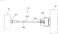
- Fig. 2 is a schematic diagram of a cable unit 24.
- the displacement meter 15 and the sensor amplifier 42 are connected to each other by the cable unit 24 illustrated in Fig. 2 .
- the cable unit 24 is provided with a sensor side connector 241, a sensor amplifier side connector 242, and a cable main body 243 connecting the sensor side connector 241 and the sensor amplifier side connector 242 to each other.
- a substrate 244 is arranged in the sensor amplifier side connector 242, and a gain resistor 26 (described later), a nonvolatile memory 25 (described later), and so on are mounted on the substrate 244.
- a cable joint 245 is provided on the cable main body 243, and the length of the cable main body 243 can be adjusted by an extension cable being inserted in accordance with the positional relationship between the control device 2 and a detector such as the load cell 14 and the displacement meter 15.
- the load cell 14 and the sensor amplifier 41 also can be connected with the same cable unit 24.
- the displacement meter 15, the cable unit 24, and the sensor amplifier 42 constitute a displacement measuring system for the test piece 10, and the displacement measuring system functions as a measuring device according to the invention.
- the displacement meter 15 and the cable unit 24 are removable with respect to the testing machine main body 1.
- the load cell 14, the cable unit 24, and the sensor amplifier 41 constitute a system measuring a test force given to the test piece 10, and the test force measuring system functions as a measuring device according to the invention.
- the load cell 14 and the cable unit 24 are removable with respect to the testing machine main body 1.
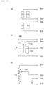
- Fig. 3 is a schematic diagram describing the structure of each detector.
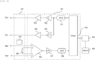
- Fig. 4 is a configuration schematic diagram of a measuring circuit.
- Fig. 5 is a block diagram describing the functional configuration of a field-programmable gate array (FPGA) 60.
- the measuring circuit illustrated in Fig. 4 is the same for every detector illustrated in Fig. 3 and will be described as the configuration of the measuring circuit of the measuring device.
- the material testing machine illustrated in Fig. 1 is provided with the load cell 14 and the displacement meter 15.
- the load cell 14 is a strain gauge type sensor measuring a test force by using a change in the electric resistance of a strain gauge.
- the load cell 14 is provided with a bridge circuit in which strain gauges R1 to R4 with the same resistance value are connected.
- the displacement meter 15 is divided into a strain gauge type displacement meter, a differential transformer type displacement meter, and a potentiometer type displacement meter depending on measurement methods, and the meters are selected in accordance with testing content.
- the strain gauge type displacement meter is provided with the bridge circuit that is illustrated in Fig. 3(a) as is the case with the load cell 14.
- the differential transformer type displacement meter is provided with a primary coil T1, secondary coils T2A and T2B, and an iron core MC moving in conjunction with elongation of the test piece 10.
- the differential transformer type displacement meter is a detector obtaining voltage output depending on displacement by using the occurrence of a difference depending on the position of the iron core MC between the induced voltages of the secondary coil T2A and the secondary coil T2B generated when the primary coil T1 is excited.
- the potentiometer type displacement meter is provided with a resistor TR and a wiper WP.
- the potentiometer type displacement meter is a detector converting a relative displacement amount of the resistor TR and the wiper WP into voltage output.
- the Sig- of the potentiometer type displacement meter is connected to a signal ground.
- the input terminals EX+ and EX- and the output terminals Sig+ and Sig-of each detector illustrated in Fig. 3 are respectively connected to corresponding connection terminals of the sensor side connector 241 of the cable unit 24.
- the sensor amplifier 42 is provided with a digital circuit based on the FPGA 60 and an analog circuit including an instrumentation amplifier 56, a low pass filter (LPF) 57, an analog-to-digital converter (ADC) 58, a digital-to-analog converter (DAC) 51, operational amplifiers 52 and 54, and power amplifiers 53 and 55.
- LPF low pass filter
- ADC analog-to-digital converter
- DAC digital-to-analog converter
- operational amplifiers 52 and 54 and power amplifiers 53 and 55.
- power amplifiers 53 and 55 Built as a logic circuit inside the FPGA 60 are a gain multiplier 69, an offset subtractor 68, and a detector circuit 61 storing waveform data sent from the FPGA 60 to the DAC 51 and extracting signal components of a test force value and an elongation value from a signal input from the ADC 58.
- the offset subtractor 68 subtracts, from digital data that went through the detector circuit 61, an offset value indicating the steady states of the test force value and the elongation value at testing initiation.
- the gain multiplier 69 is mainly to adjust a gain difference attributable to an individual difference in detectors of the same type and sensitivity.
- a FPGA is used as a device realizing a logic circuit processing a digital signal in this embodiment, another programmable logic device (PLD) capable of rewriting an internal circuit and a microcomputer performing digital signal processing with software may be used instead.
- PLD programmable logic device
- the cable unit 24 is provided with the nonvolatile memory 25 and the gain resistor 26 determining the gain of the instrumentation amplifier 56 of the sensor amplifier 42.
- Information on the type of each detector and information related thereto are stored in the nonvolatile memory 25.
- a waveform signal of a drive voltage input to the input terminals EX+ and EX- of each detector is transmitted from the FPGA 60 to the DAC 51.
- a waveform generated from the DAC 51 is input to the operational amplifiers 52 and 54, turned into a drive waveform as a plus or minus subject focusing on zero volt, and then amplified by the power amplifiers 53 and 55 and supplied to a detector as an excitation signal.
- a signal output from the output terminals Sig+ and Sig- of a detector is input to the instrumentation amplifier 56 and a difference is retrieved.
- the LPF 57 removes a component exceeding the Nyquist frequency of the ADC 58, and then the signal is converted into a digital signal by the ADC 58 and input to the FPGA 60.
- the test force value or the elongation value (displacement amount) of the test piece 10 is displayed on the display 48 via the control panel 40.
- the information stored in the nonvolatile memory 25 of the substrate 244, such as detector model information, is read into the FPGA 60.
- the cable unit 24 and a detector are used as a pair, and the resistance value of the gain resistor 26 is a value determined in advance depending on detectors to be optimal in magnitude for the analog circuit in the sensor amplifier 42.
- the gain resistor 26 provided in the cable unit 24 determines (or sets) the gain of the instrumentation amplifier 56 to which the signal output from the output terminals Sig+ and Sig- of each detector is input.
- an analog circuit in an earlier stage than the ADC 58 of the sensor amplifier 42 is designed, for example, not to be saturated even when the displacement meter 15 that has the highest sensitivity among the displacement meters 15 of the same measurement method is connected. Accordingly, once the resistance value of the instrumentation amplifier 56 is fixed on the sensor amplifier side, the full scale of the ADC 58 cannot be used, which is a problem, when the displacement meter 15 with low sensitivity is connected.
- the full scale of the ADC 58 can be used to the maximum extent possible regardless of the sensitivity of the displacement meter 15. Therefore, the displacement meters 15 based on different measurement methods as illustrated in Figs. 3(a) to 3(c) can be connected.
- the cable unit 24 described with reference to Fig. 4 is provided with the nonvolatile memory 25 storing information on a detector connected to the sensor amplifier 42 and the gain resistor 26 determining the gain of the instrumentation amplifier 56 of the sensor amplifier 42 in accordance with the type and full scale of the detector.
- a circuit for electrical measuring circuit calibration is provided will be additionally described below.
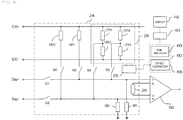
- Fig. 6 is a configuration schematic diagram illustrating the circuit configuration of the cable unit 24 for performing electrical calibration.
- the cable unit 24 is provided with an electrical calibration circuit having a calibration bridge 28 of four resistors CR1 to CR4 and shunt resistances SR1 and SR2 as calibration resistors, switches S1 and S2 switching the connection state of signal input from each detector to the instrumentation amplifier 56, and switches S3 to S6 switching the connection state of the electrical calibration circuit and the instrumentation amplifier 56.
- the switch S3 and the switch S4 selectively connect the calibration bridge 28 to the instrumentation amplifier 56.
- the switch S5 selectively connects the shunt resistance SR1 in parallel to the calibration bridge 28.
- the switch S6 selectively connects the shunt resistance SR2 in parallel to the calibration bridge 28.
- the shunt resistance SR1 is a calibration resistance at a time when the direction of displacement of the test piece 10 is to the compression side
- the shunt resistance SR2 is a calibration resistance at a time when the direction of displacement of the test piece 10 is to the tension side.
- a bias resistance BR is placed on the path through which an input signal of the cable unit 24 is output to the instrumentation amplifier 56 and supplies an input bias current to the instrumentation amplifier.
- Various electrical elements built into the cable unit 24 are mounted on a printed substrate 244 provided in the sensor amplifier side connector 242.
- Physical quantity measuring circuit calibration is divided into actual displacement- and actual test force-based calibration and shunt resistance-based electrical calibration.
- the actual displacement- and actual test force-based calibration which is performed by a material testing machine manufacturer or maintenance contractor, is to actually give calibrated actual displacement or the like to a detector before material testing machine shipment and during maintenance based on detector removal from the testing machine main body 1.
- the electrical calibration which is performed by a material testing machine user, is to adjust the gain of a sensor amplifier by electrically reproducing virtual physical displacement.
- the actual displacement- and actual test force-based calibration will be described first.
- the cable unit 24 is connected to a detector and an accuracy-guaranteed calibrator (not illustrated) for giving actual displacement or actual test force is attached.
- the switches S1 and S2 illustrated in Fig. 6 are left closed and the switches S3 to S6 are left open.
- Zero load or zero elongation is given to the detector in this state, and the offset value at which the value of the display 48 at this time becomes zero, that is, a value subtracted by the offset subtractor 68 of the FPGA 60 is obtained.
- the offset value is stored in the nonvolatile memory 25 of the cable unit 24.
- the offset value indicates the steady states of a test force value and an elongation value at testing initiation.
- a rated capacity-equivalent (full scale) load is given to the detector by the calibrator, and a value multiplied by the gain multiplier 69 of the FPGA 60 is adjusted such that the display 48 shows a full scale value.
- the switch S1 and the switch S2 are opened and the switch S3 and the switch S4 are closed.
- a state is made where a signal from the detector is disconnected and the calibration bridge 28 is connected.
- the value subtracted by the offset subtractor 68 of the FPGA 60 is adjusted such that the display 48 shows zero.
- either the switch S5 or the switch S6 is closed depending on whether the direction of displacement or test force is to either the tension side or the compression side and the calibration bridge 28 is distorted in a pseudo manner, and the value that the display 48 shows at that time is stored in the nonvolatile memory 25 of the cable unit 24.
- the gain of the sensor amplifier is confirmed first by the measuring circuit being calibrated with actual displacement and actual test force. Subsequently, input to the instrumentation amplifier 56 is switched from the detector to the calibration bridge 28 and an electrical calibration target value (value shown by the display 48 when the shunt resistance was given to the calibration bridge 28) is created by the shunt resistance SR1 or the shunt resistance SR2 being used.
- a state is made where the switch S1 and the switch S2 are open, the switch S3 and the switch S4 are closed, and the switch S5 and the switch S6 are open.
- a state is made where input from the detector is disconnected and the calibration bridge 28 is connected.
- the value subtracted by the offset subtractor 68 is adjusted such that the value of the display 48 shows zero.
- Either the switch S5 or the switch S6 is closed depending on whether the direction of displacement or test force is to either the tension side or the compression side and a pseudo strain is given to the calibration bridge 28.
- the value multiplied by the gain multiplier 69 of the FPGA 60 is adjusted such that the value of the display 48 at this time corresponds to the value shown by the display 48 and stored in the nonvolatile memory 25, that is, the value shown by the display 48 when a rated capacity-equivalent load was given during the actual displacement-based calibration.
- the gain of the sensor amplifier is adjusted by the calibration bridge 28 and the shunt resistance SR1 or the shunt resistance SR2 being used such that the value shown by the display 48 corresponds to the target value previously stored in the nonvolatile memory 25. Subsequently, physical quantity measurement is performed with the input source of the signal to the instrumentation amplifier 56 switched to the detector.
- an electrical element required for measuring circuit calibration is built into the cable unit 24. Accordingly, especially during the shunt resistance-based electrical calibration performed on a user side, the circuit in the cable unit 24 is not affected at all, even when a user touches the detector during the execution of the calibration, since the switch S1 and the switch S2 are open. Therefore, the electrical calibration can still be executed even in a state where a user touches the detector due to attachment of the test piece 10 or the like. In addition, material testing work efficiency is improved as testing preparation and electrical calibration are performed together. Furthermore, since the electrical element required for measuring circuit calibration is built into the cable unit 24, electrical calibration of a differential transformer type displacement meter, which is not easy with the related art, can be performed with ease.
- Conventional electrical calibration is executed by a user performing an execution operation after confirming that the testing machine main body 1 and a detector are in a physically stable state.
- electrical calibration can be executed at a preset timing such as 10 minutes after energization and immediately after testing.
- detector identification such as detector types and specifications
- the gain resistor 26 of the cable unit 24 is placed in accordance with the types and full scales of detectors, and thus any of the detectors that are strain gauge type load cells, strain gauge type displacement meters, differential transformer type displacement meters, and potentiometer type displacement meters can be connected to the sensor amplifier by the cable unit 24 being used and the accuracy and resolution on the sensor amplifier side can be improved.
Landscapes
- Physics & Mathematics (AREA)
- Health & Medical Sciences (AREA)
- Life Sciences & Earth Sciences (AREA)
- Chemical & Material Sciences (AREA)
- Analytical Chemistry (AREA)
- Biochemistry (AREA)
- General Health & Medical Sciences (AREA)
- General Physics & Mathematics (AREA)
- Immunology (AREA)
- Pathology (AREA)
- Engineering & Computer Science (AREA)
- Power Engineering (AREA)
- Manufacturing & Machinery (AREA)
- Investigating Strength Of Materials By Application Of Mechanical Stress (AREA)
Abstract
Description
- The present invention relates to a measuring device and a material testing machine provided with a detector converting a physical quantity into an electric signal.
- Arranged in a material testing machine performing material testing are a load mechanism giving a test load to a test piece and a plurality of detectors converting a physical quantity into an electric signal, examples of the detectors including a test force detector measuring a test force given to the test piece by the load mechanism and a displacement meter detecting displacement generated in the test piece. A physical quantity measuring system for material testing is configured by the detectors being connected to a testing machine controller controlling the entire material testing machine via an amplifier (see Patent Document 1).
- In the related art, sensor amplifiers should be individually prepared, in view of the difference between the physical quantity measurement methods of the detectors, on a control device side for each detector to be connected to the control device of the testing machine. In this regard, an amplifier device for a displacement meter to which both a strain gauge type displacement meter and a differential transformer type displacement meter can be connected has been proposed in
Patent Document 2 as a displacement detector detecting displacement generated in a test piece. - This type of detector is appropriately used through replacement with respect to a material testing machine main body depending on the types of material testing, and thus a measuring circuit constituting a physical quantity measuring system should be calibrated when the detector is installed in the testing machine main body or from time to time as necessary. In the case of load cells, calibration target value creation and so on are performed, by a load cell supplier or a supplier of apparatuses including load cells, by methods such as a method for inputting a rated capacity equivalent to a load cell and a method for actually giving a known load to a load cell. A load cell user performs work based on calibration information provided by the supplier in order to adjust the gain of a load cell-connected control device side amplifier and confirm the accuracy of test force display at a time when the known load is given.
- The electrical measuring circuit calibration required for the user side operation is cumbersome for some users. Proposed in this regard is a control device in which a shunt resistance and a reference bridge circuit for amplifier calibration are provided at a part where a strain gauge type detector is connected so that calibration of an amplifier receiving input from the strain gauge type detector is automated (see Patent Document 3). Also proposed is a material testing machine with which amplifier gain adjustment can be automatically performed by a cable unit being provided with calibration impedance in a case where a differential transformer or a capacitive sensor is used for test piece displacement measurement (see Patent Document 4).
-
- Patent Document 1:
JP-A-2007-218809 - Patent Document 2:
JP-A-2011-169774 - Patent Document 3:
JP-A-2007-78560 - Patent Document 4:
JP-A-2009-250678 - Sensitivity, which is an output-to-input ratio, varies with displacement meter structures and measurement methods.
Patent Document 2 adopts a method for switching the gain of an instrumentation amplifier with respect to a significant sensitivity difference (such as 100 times or more) between displacement meters using different measurement methods. However, gain adjustment is performed with a digital circuit following analog-to-digital conversion with respect to a relatively small sensitivity difference (such as approximately 10 times) between displacement meters using the same measurement method. Accordingly, an AD converter and an analog circuit in an earlier stage than the AD converter are designed not to be saturated despite connection of a displacement meter with the highest assumed sensitivity and, when a low-sensitivity displacement meter is connected, the full scale of the AD converter cannot be sufficiently used. - In addition, in a strain gauge type displacement meter and a load cell that use the same measurement method despite different physical quantities to be measured, the load cell requires high resolution, and thus resolution is insufficient even when the load cell is connected to an amplifier device for a displacement meter as in
Patent Document 2. Accordingly, the amplifier device for a displacement meter cannot be used for the load cell. Furthermore, the amplifier device for a displacement meter disclosed inPatent Document 2, which responds to strain gauge and differential transformer type displacement meters, is too sensitive and cannot be used as it is with regard to a potentiometer type displacement meter. - Regarding electrical measuring circuit calibration, in
Patent Document 3, a cable for connection between a strain gauge type displacement meter and an amplifier is provided with a circuit for amplifier calibration. No electrical measuring circuit calibration, however, can be performed even when the differential transformer type displacement meter is connected to the amplifier by means of the cable. AlthoughPatent Document 4 has proposed a circuit that is capable of performing electrical calibration in a case where a differential transformer type displacement meter is connected, this technique uses amplifier side impedance as well during calibration, and thus has problems such as the necessity of a circuit therefor in an earlier stage than an instrumentation amplifier, the necessity of a change in cable side impedance reflecting the type and full scale of the differential transformer type displacement meter, and the necessity of the same differential transformer iron core position during calibration. - The invention has been made to solve the above problems, and an object thereof is to provide a measuring device and a material testing machine with which an amplifier can be used at an optimal gain even when any one of detectors using different measurement methods is connected.
- Another object of the invention is to provide a measuring device and a material testing machine with which electrical measuring circuit calibration can be automatically performed even in a case where detectors have different types and full scales.
- According to the invention described in
claim 1, a measuring device includes a detector converting a change in physical quantity generated in a measurement object into an electric signal and outputting the electric signal, a sensor amplifier to which the output signal of the detector is input, and a cable unit connecting the detector and the sensor amplifier to each other, in which the cable unit includes a nonvolatile memory storing information on the detector and a resistor determining a gain of the instrumentation amplifier to a gain depending on the information on the detector. - According to the invention described in
claim 2, in the measuring device according to the invention described inclaim 1, the cable unit includes an electrical calibration circuit having a calibration bridge and a calibration resistance, a switch switching a state of the signal input from the detector to the instrumentation amplifier, and a switch switching a state of connection between the electrical calibration circuit and the instrumentation amplifier. - According to the invention described in
claim 3, a material testing machine performs material testing, is provided with a load mechanism giving a test force to a test piece, and is provided with the measuring device according to the invention described inclaim - According to the invention described in
claim 4, in the material testing machine according to the invention described inclaim 3, the measuring device is a measuring device including a load cell detecting the test force given to the test piece or a measuring device including a displacement meter detecting displacement generated in the test piece. - According to the invention described in
claim 1, the nonvolatile memory storing the information on the connected detector and the resistor determining the gain of the instrumentation amplifier are placed in the cable unit and the resistor in the cable unit determines the gain of the instrumentation amplifier such that the magnitude of the signal that the sensor amplifier receives from the detector becomes a magnitude optimal for an analog circuit in the sensor amplifier. Accordingly, the amplifier can be used at an optimal gain for every detector electrically connectable to the sensor amplifier. - According to the invention described in
claim 2, the electrical calibration circuit is provided in the cable unit, and thus so-called shunt calibration can be performed for any connected detector. In other words, with the electrical calibration circuit in the cable unit, electrical calibration can be performed even with respect to detectors that could not be electrically calibrated in the past. Furthermore, the input from the detector side can be disconnected by the switch, and thus a stationary state on the detector side does not have to be confirmed during electrical calibration unlike in the past. Accordingly, electrical calibration can be performed regardless of the state on the detector side. Therefore, the gain on the sensor amplifier side can be accurately adjusted. - According to the invention described in
claim 3, the measuring device with which the amplifier can be used at an optimal gain is provided, and thus the accuracy of a measured material testing value can be improved along with resolution. - According to the invention described in
claim 4, the amplifier can be used at an optimal amplifier gain at which the capabilities of the load cell and the displacement meter can be appropriately demonstrated, and thus the accuracy of test force and elongation values measured during material testing can be improved. -
-
Fig. 1 is a schematic diagram of a material testing machine. -
Fig. 2 is a schematic diagram of acable unit 24. -
Fig. 3 is a schematic diagram describing the structure of each detector. -
Fig. 4 is a configuration schematic diagram illustrating the configuration of a measuring circuit. -
Fig. 5 is a block diagram describing the functional configuration of aFPGA 60. -
Fig. 6 is a configuration schematic diagram illustrating the circuit configuration of thecable unit 24 for performing electrical calibration. - Hereinafter, an embodiment of the invention will be described with reference to accompanying drawings.
Fig. 1 is a schematic diagram of a material testing machine. - A testing machine
main body 1 and acontrol device 2 constitute this material testing machine. The testing machinemain body 1 is provided with a table 16, a pair ofscrew rods crosshead 13 movable along thescrew rods load mechanism 30 for giving a load to atest piece 10 as a measurement object by moving thecrosshead 13, and aload cell 14 and adisplacement meter 15 as detectors converting a change in physical quantity in thetest piece 10 into an electric signal. - The
crosshead 13 is connected to the pair ofscrew rods Worm reducers load mechanism 30 are connected to the lower end portions of thescrew rods worm reducers servomotor 31, which is a driving source for theload mechanism 30, and are configured such that rotation of theservomotor 31 is transmitted to the pair ofscrew rods worm reducers servomotor 31, the pair ofscrew rods crosshead 13 moves upward or downward along thescrew rods - An
upper gripper 21 for gripping the upper end portion of thetest piece 10 is attached to thecrosshead 13. Alower gripper 22 for gripping the lower end portion of thetest piece 10 is attached to the table 16. In a case where a tensile test is performed, thetest piece 10 is loaded with a test force (tensile test force) by thecrosshead 13 being raised in a state where both end portions of thetest piece 10 are gripped by theupper gripper 21 and thelower gripper 22. - A computer, a sequencer, and peripheral equipment thereof constitute the
control device 2, and thecontrol device 2 is provided with acontrol panel 40 that has a CPU executing a logical operation, a ROM storing an operation program required for apparatus control, a RAM temporarily storing data and so on during control, and the like and controls the entire apparatus. In addition, thecontrol device 2 is provided with asensor amplifier 41 for a load cell, asensor amplifier 42 for thedisplacement meter 15, and adisplay 48 for displaying a displacement amount and a test force detected by theload cell 14 and thedisplacement meter 15. - When the
load mechanism 30 is operated, the test force that acts on thetest piece 10 with both ends gripped by theupper gripper 21 and thelower gripper 22 is detected by theload cell 14 and an output signal of theload cell 14 is input to thecontrol panel 40 via thesensor amplifier 41. In addition, the displacement amount that is generated in thetest piece 10 is measured by thedisplacement meter 15 and an output signal of thedisplacement meter 15 is input to thecontrol panel 40 via thesensor amplifier 42. - In the
control panel 40, data processing is executed by the CPU with test force data and displacement amount data from theload cell 14 and thedisplacement meter 15 captured. In addition, in thecontrol panel 40, feedback control of rotational drive of theservomotor 31 is executed by means of operation of a control program stored in the ROM and a digital circuit and fluctuations in the test force and the displacement amount input as digital data. -
Fig. 2 is a schematic diagram of acable unit 24. - The
displacement meter 15 and thesensor amplifier 42 are connected to each other by thecable unit 24 illustrated inFig. 2 . Thecable unit 24 is provided with asensor side connector 241, a sensoramplifier side connector 242, and a cablemain body 243 connecting thesensor side connector 241 and the sensoramplifier side connector 242 to each other. Asubstrate 244 is arranged in the sensoramplifier side connector 242, and a gain resistor 26 (described later), a nonvolatile memory 25 (described later), and so on are mounted on thesubstrate 244. Acable joint 245 is provided on the cablemain body 243, and the length of the cablemain body 243 can be adjusted by an extension cable being inserted in accordance with the positional relationship between thecontrol device 2 and a detector such as theload cell 14 and thedisplacement meter 15. Although an example in which thedisplacement meter 15 and thesensor amplifier 42 are connected to each other is illustrated inFig. 2 , theload cell 14 and thesensor amplifier 41 also can be connected with thesame cable unit 24. - The
displacement meter 15, thecable unit 24, and thesensor amplifier 42 constitute a displacement measuring system for thetest piece 10, and the displacement measuring system functions as a measuring device according to the invention. Thedisplacement meter 15 and thecable unit 24 are removable with respect to the testing machinemain body 1. In addition, theload cell 14, thecable unit 24, and thesensor amplifier 41 constitute a system measuring a test force given to thetest piece 10, and the test force measuring system functions as a measuring device according to the invention. Theload cell 14 and thecable unit 24 are removable with respect to the testing machinemain body 1. -
Fig. 3 is a schematic diagram describing the structure of each detector.Fig. 4 is a configuration schematic diagram of a measuring circuit.Fig. 5 is a block diagram describing the functional configuration of a field-programmable gate array (FPGA) 60. The measuring circuit illustrated inFig. 4 is the same for every detector illustrated inFig. 3 and will be described as the configuration of the measuring circuit of the measuring device. - The material testing machine illustrated in
Fig. 1 is provided with theload cell 14 and thedisplacement meter 15. Theload cell 14 is a strain gauge type sensor measuring a test force by using a change in the electric resistance of a strain gauge. As illustrated inFig. 3(a) , theload cell 14 is provided with a bridge circuit in which strain gauges R1 to R4 with the same resistance value are connected. - The
displacement meter 15 is divided into a strain gauge type displacement meter, a differential transformer type displacement meter, and a potentiometer type displacement meter depending on measurement methods, and the meters are selected in accordance with testing content. The strain gauge type displacement meter is provided with the bridge circuit that is illustrated inFig. 3(a) as is the case with theload cell 14. As illustrated inFig. 3(b) , the differential transformer type displacement meter is provided with a primary coil T1, secondary coils T2A and T2B, and an iron core MC moving in conjunction with elongation of thetest piece 10. The differential transformer type displacement meter is a detector obtaining voltage output depending on displacement by using the occurrence of a difference depending on the position of the iron core MC between the induced voltages of the secondary coil T2A and the secondary coil T2B generated when the primary coil T1 is excited. As illustrated inFig. 3(c) , the potentiometer type displacement meter is provided with a resistor TR and a wiper WP. The potentiometer type displacement meter is a detector converting a relative displacement amount of the resistor TR and the wiper WP into voltage output. The Sig- of the potentiometer type displacement meter is connected to a signal ground. The input terminals EX+ and EX- and the output terminals Sig+ and Sig-of each detector illustrated inFig. 3 are respectively connected to corresponding connection terminals of thesensor side connector 241 of thecable unit 24. - The
sensor amplifier 42 is provided with a digital circuit based on theFPGA 60 and an analog circuit including aninstrumentation amplifier 56, a low pass filter (LPF) 57, an analog-to-digital converter (ADC) 58, a digital-to-analog converter (DAC) 51,operational amplifiers power amplifiers FPGA 60 are again multiplier 69, an offsetsubtractor 68, and adetector circuit 61 storing waveform data sent from theFPGA 60 to theDAC 51 and extracting signal components of a test force value and an elongation value from a signal input from theADC 58. The offsetsubtractor 68 subtracts, from digital data that went through thedetector circuit 61, an offset value indicating the steady states of the test force value and the elongation value at testing initiation. Thegain multiplier 69 is mainly to adjust a gain difference attributable to an individual difference in detectors of the same type and sensitivity. Although a FPGA is used as a device realizing a logic circuit processing a digital signal in this embodiment, another programmable logic device (PLD) capable of rewriting an internal circuit and a microcomputer performing digital signal processing with software may be used instead. - The
cable unit 24 is provided with thenonvolatile memory 25 and thegain resistor 26 determining the gain of theinstrumentation amplifier 56 of thesensor amplifier 42. Information on the type of each detector and information related thereto (such as model and full scale) are stored in thenonvolatile memory 25. - A waveform signal of a drive voltage input to the input terminals EX+ and EX- of each detector is transmitted from the
FPGA 60 to theDAC 51. A waveform generated from theDAC 51 is input to theoperational amplifiers power amplifiers instrumentation amplifier 56 and a difference is retrieved. Then, theLPF 57 removes a component exceeding the Nyquist frequency of theADC 58, and then the signal is converted into a digital signal by theADC 58 and input to theFPGA 60. Subsequently, after signal processing in theFPGA 60, the test force value or the elongation value (displacement amount) of thetest piece 10 is displayed on thedisplay 48 via thecontrol panel 40. - Once the sensor
amplifier side connector 242 of thecable unit 24 is connected to thesensor amplifier 42, the information stored in thenonvolatile memory 25 of thesubstrate 244, such as detector model information, is read into theFPGA 60. Thecable unit 24 and a detector are used as a pair, and the resistance value of thegain resistor 26 is a value determined in advance depending on detectors to be optimal in magnitude for the analog circuit in thesensor amplifier 42. - Not only a circuit element on the sensor amplifier side but also the
gain resistor 26 provided in thecable unit 24 determines (or sets) the gain of theinstrumentation amplifier 56 to which the signal output from the output terminals Sig+ and Sig- of each detector is input. In conventional apparatuses, an analog circuit in an earlier stage than theADC 58 of thesensor amplifier 42 is designed, for example, not to be saturated even when thedisplacement meter 15 that has the highest sensitivity among thedisplacement meters 15 of the same measurement method is connected. Accordingly, once the resistance value of theinstrumentation amplifier 56 is fixed on the sensor amplifier side, the full scale of theADC 58 cannot be used, which is a problem, when thedisplacement meter 15 with low sensitivity is connected. However, by the gain of theinstrumentation amplifier 56 being set by thegain resistor 26 provided in thecable unit 24 as in the measuring device according to the invention, the full scale of theADC 58 can be used to the maximum extent possible regardless of the sensitivity of thedisplacement meter 15. Therefore, thedisplacement meters 15 based on different measurement methods as illustrated inFigs. 3(a) to 3(c) can be connected. - The
cable unit 24 described with reference toFig. 4 is provided with thenonvolatile memory 25 storing information on a detector connected to thesensor amplifier 42 and thegain resistor 26 determining the gain of theinstrumentation amplifier 56 of thesensor amplifier 42 in accordance with the type and full scale of the detector. A case where a circuit for electrical measuring circuit calibration is provided will be additionally described below.Fig. 6 is a configuration schematic diagram illustrating the circuit configuration of thecable unit 24 for performing electrical calibration. - The
cable unit 24 is provided with an electrical calibration circuit having acalibration bridge 28 of four resistors CR1 to CR4 and shunt resistances SR1 and SR2 as calibration resistors, switches S1 and S2 switching the connection state of signal input from each detector to theinstrumentation amplifier 56, and switches S3 to S6 switching the connection state of the electrical calibration circuit and theinstrumentation amplifier 56. The switch S3 and the switch S4 selectively connect thecalibration bridge 28 to theinstrumentation amplifier 56. The switch S5 selectively connects the shunt resistance SR1 in parallel to thecalibration bridge 28. The switch S6 selectively connects the shunt resistance SR2 in parallel to thecalibration bridge 28. The shunt resistance SR1 is a calibration resistance at a time when the direction of displacement of thetest piece 10 is to the compression side, and the shunt resistance SR2 is a calibration resistance at a time when the direction of displacement of thetest piece 10 is to the tension side. In addition, a bias resistance BR is placed on the path through which an input signal of thecable unit 24 is output to theinstrumentation amplifier 56 and supplies an input bias current to the instrumentation amplifier. Various electrical elements built into thecable unit 24 are mounted on a printedsubstrate 244 provided in the sensoramplifier side connector 242. - Calibration of a physical quantity measuring circuit including the sensor amplifier of each detector by means of the
cable unit 24 will be described below. Physical quantity measuring circuit calibration is divided into actual displacement- and actual test force-based calibration and shunt resistance-based electrical calibration. The actual displacement- and actual test force-based calibration, which is performed by a material testing machine manufacturer or maintenance contractor, is to actually give calibrated actual displacement or the like to a detector before material testing machine shipment and during maintenance based on detector removal from the testing machinemain body 1. The electrical calibration, which is performed by a material testing machine user, is to adjust the gain of a sensor amplifier by electrically reproducing virtual physical displacement. - The actual displacement- and actual test force-based calibration will be described first. The
cable unit 24 is connected to a detector and an accuracy-guaranteed calibrator (not illustrated) for giving actual displacement or actual test force is attached. At this time, the switches S1 and S2 illustrated inFig. 6 are left closed and the switches S3 to S6 are left open. Zero load or zero elongation is given to the detector in this state, and the offset value at which the value of thedisplay 48 at this time becomes zero, that is, a value subtracted by the offsetsubtractor 68 of theFPGA 60 is obtained. Then, the offset value is stored in thenonvolatile memory 25 of thecable unit 24. The offset value indicates the steady states of a test force value and an elongation value at testing initiation. Subsequently, a rated capacity-equivalent (full scale) load is given to the detector by the calibrator, and a value multiplied by thegain multiplier 69 of theFPGA 60 is adjusted such that thedisplay 48 shows a full scale value. - Once the gain adjustment for the
gain multiplier 69 is over, the switch S1 and the switch S2 are opened and the switch S3 and the switch S4 are closed. In other words, a state is made where a signal from the detector is disconnected and thecalibration bridge 28 is connected. The value subtracted by the offsetsubtractor 68 of theFPGA 60 is adjusted such that thedisplay 48 shows zero. Then, either the switch S5 or the switch S6 is closed depending on whether the direction of displacement or test force is to either the tension side or the compression side and thecalibration bridge 28 is distorted in a pseudo manner, and the value that thedisplay 48 shows at that time is stored in thenonvolatile memory 25 of thecable unit 24. Subsequently, all of the switches S3 to S6 are opened and the switch S1 and the switch S2 are closed. Then, the value held by the offsetsubtractor 68 at this time to be subtracted from the signal input from thedetector circuit 61 is written back to the value previously stored in the nonvolatile memory 25 (offset value). Then, the actual displacement- and actual test force-based calibration terminates. - During the actual displacement- and actual test force-based calibration, the gain of the sensor amplifier is confirmed first by the measuring circuit being calibrated with actual displacement and actual test force. Subsequently, input to the
instrumentation amplifier 56 is switched from the detector to thecalibration bridge 28 and an electrical calibration target value (value shown by thedisplay 48 when the shunt resistance was given to the calibration bridge 28) is created by the shunt resistance SR1 or the shunt resistance SR2 being used. - The shunt resistance-based electrical calibration will be described below. Firstly, a state is made where the switch S1 and the switch S2 are open, the switch S3 and the switch S4 are closed, and the switch S5 and the switch S6 are open. In other words, a state is made where input from the detector is disconnected and the
calibration bridge 28 is connected. In this state, the value subtracted by the offsetsubtractor 68 is adjusted such that the value of thedisplay 48 shows zero. Either the switch S5 or the switch S6 is closed depending on whether the direction of displacement or test force is to either the tension side or the compression side and a pseudo strain is given to thecalibration bridge 28. The value multiplied by thegain multiplier 69 of theFPGA 60 is adjusted such that the value of thedisplay 48 at this time corresponds to the value shown by thedisplay 48 and stored in thenonvolatile memory 25, that is, the value shown by thedisplay 48 when a rated capacity-equivalent load was given during the actual displacement-based calibration. - Once the gain adjustment for the
gain multiplier 69 is over, a state is made where the switch S3 to switch S6 are open and the switch S1 and the switch S2 are closed. Then, the value held by the offsetsubtractor 68 at this time to be subtracted from the signal input from thedetector circuit 61 is written back to the value previously stored in the nonvolatile memory 25 (offset value). Then, the shunt resistance-based electrical calibration terminates. - During the execution of the electrical calibration, the gain of the sensor amplifier is adjusted by the
calibration bridge 28 and the shunt resistance SR1 or the shunt resistance SR2 being used such that the value shown by thedisplay 48 corresponds to the target value previously stored in thenonvolatile memory 25. Subsequently, physical quantity measurement is performed with the input source of the signal to theinstrumentation amplifier 56 switched to the detector. - As described above, according to the invention, an electrical element required for measuring circuit calibration is built into the
cable unit 24. Accordingly, especially during the shunt resistance-based electrical calibration performed on a user side, the circuit in thecable unit 24 is not affected at all, even when a user touches the detector during the execution of the calibration, since the switch S1 and the switch S2 are open. Therefore, the electrical calibration can still be executed even in a state where a user touches the detector due to attachment of thetest piece 10 or the like. In addition, material testing work efficiency is improved as testing preparation and electrical calibration are performed together. Furthermore, since the electrical element required for measuring circuit calibration is built into thecable unit 24, electrical calibration of a differential transformer type displacement meter, which is not easy with the related art, can be performed with ease. - Conventional electrical calibration is executed by a user performing an execution operation after confirming that the testing machine
main body 1 and a detector are in a physically stable state. With the invention, however, electrical calibration can be executed at a preset timing such as 10 minutes after energization and immediately after testing. - Information required for detector identification, such as detector types and specifications, can be stored in the
nonvolatile memory 25 of thecable unit 24 and thegain resistor 26 of thecable unit 24 is placed in accordance with the types and full scales of detectors, and thus any of the detectors that are strain gauge type load cells, strain gauge type displacement meters, differential transformer type displacement meters, and potentiometer type displacement meters can be connected to the sensor amplifier by thecable unit 24 being used and the accuracy and resolution on the sensor amplifier side can be improved. -
- 1
- Testing machine main body
- 2
- Control device
- 10
- Test piece
- 11
- Screw rod
- 12
- Screw rod
- 13
- Crosshead
- 14
- Load cell
- 15
- Displacement meter
- 16
- Table
- 21
- Upper gripper
- 22
- Lower gripper
- 24
- Cable unit
- 25
- Nonvolatile memory
- 26
- Gain resistor
- 28
- Calibration bridge
- 30
- Load mechanism
- 31
- Servomotor
- 32
- Worm reducer
- 33
- Worm reducer
- 40
- Control panel
- 41
- Sensor amplifier
- 42
- Sensor amplifier
- 48
- Display
- 51
- DAC
- 52
- Operational amplifier
- 53
- Power amplifier
- 54
- Operational amplifier
- 55
- Power amplifier
- 56
- Instrumentation amplifier
- 57
- LPF
- 58
- ADC
- 60
- FPGA
- 61
- Detector circuit
- 68
- Offset subtractor
- 69
- Gain multiplier
Claims (4)
- A measuring device comprising:a detector converting a change in physical quantity generated in a measurement object into an electric signal and outputting the electric signal;a sensor amplifier to which the output signal of the detector is input; anda cable unit connecting the detector and the sensor amplifier to each other,wherein the cable unit includes a nonvolatile memory storing information on the detector and a resistor determining a gain of the instrumentation amplifier to a gain depending on the information on the detector.
- The measuring device according to claim 1, wherein the cable unit includes:an electrical calibration circuit having a calibration bridge and a calibration resistance;a switch switching a state of the signal input from the detector to the instrumentation amplifier; anda switch switching a state of connection between the electrical calibration circuit and the instrumentation amplifier.
- A material testing machine performing material testing, provided with a load mechanism giving a test force to a test piece, and provided with the measuring device according to claim 1 or 2.
- The material testing machine according to claim 3,
wherein the measuring device is a measuring device including a load cell detecting the test force given to the test piece or a measuring device including a displacement meter detecting displacement generated in the test piece.
Applications Claiming Priority (1)
| Application Number | Priority Date | Filing Date | Title |
|---|---|---|---|
| PCT/JP2016/055472 WO2017145295A1 (en) | 2016-02-24 | 2016-02-24 | Measurement device and material tester |
Publications (3)
| Publication Number | Publication Date |
|---|---|
| EP3421966A1 true EP3421966A1 (en) | 2019-01-02 |
| EP3421966A4 EP3421966A4 (en) | 2019-09-04 |
| EP3421966B1 EP3421966B1 (en) | 2020-11-25 |
Family
ID=59684894
Family Applications (1)
| Application Number | Title | Priority Date | Filing Date |
|---|---|---|---|
| EP16891452.1A Active EP3421966B1 (en) | 2016-02-24 | 2016-02-24 | Measurement device and material tester |
Country Status (4)
| Country | Link |
|---|---|
| US (1) | US10697872B2 (en) |
| EP (1) | EP3421966B1 (en) |
| JP (1) | JP6477969B2 (en) |
| WO (1) | WO2017145295A1 (en) |
Families Citing this family (3)
| Publication number | Priority date | Publication date | Assignee | Title |
|---|---|---|---|---|
| US10962623B1 (en) * | 2017-05-17 | 2021-03-30 | Heathkit Company, Inc. | Accurate and model-based measurement and management systems and methods |
| JP7472505B2 (en) * | 2020-01-24 | 2024-04-23 | 株式会社島津製作所 | Material testing machine and method for controlling material testing machine |
| CN114878335B (en) * | 2022-07-11 | 2022-09-30 | 杭州应敏科技有限公司 | Cable tensile strength test device |
Family Cites Families (14)
| Publication number | Priority date | Publication date | Assignee | Title |
|---|---|---|---|---|
| JPS6178076A (en) * | 1984-09-25 | 1986-04-21 | 松下電工株式会社 | Connection structure for signal line |
| JPH0333336U (en) * | 1989-08-09 | 1991-04-02 | ||
| US5606515A (en) * | 1993-02-03 | 1997-02-25 | Instron Corporation | Sensor conditioning circuitry for use with electrically excited transducers |
| JP3465832B2 (en) * | 1995-03-10 | 2003-11-10 | 株式会社エー・アンド・デイ | Load cell and material testing machine |
| EP0897110A3 (en) * | 1997-08-13 | 2000-01-12 | Japan Tobacco Inc. | Material testing machine |
| JP4508993B2 (en) * | 2005-09-15 | 2010-07-21 | 株式会社島津製作所 | Control device for material testing machine |
| JP4697433B2 (en) | 2006-02-17 | 2011-06-08 | 株式会社島津製作所 | Material testing machine |
| JP2009250678A (en) * | 2008-04-02 | 2009-10-29 | Shimadzu Corp | Materials testing machine |
| JP4957645B2 (en) * | 2008-05-12 | 2012-06-20 | 株式会社島津製作所 | Material testing machine |
| JP5240216B2 (en) * | 2010-02-19 | 2013-07-17 | 株式会社島津製作所 | Amplifier device for displacement meter |
| JP6094463B2 (en) * | 2013-12-09 | 2017-03-15 | 株式会社島津製作所 | Material testing machine |
| US10168371B2 (en) * | 2017-04-04 | 2019-01-01 | Pa&E, Hermetic Solutions Group, Llc | System and methods for determining the impact of moisture on dielectric sealing material of downhole electrical feedthrough packages |
| WO2019070659A1 (en) * | 2017-10-03 | 2019-04-11 | Waters Technologies Corporation | Automatic system compliance estimation and correction for mechanical testing systems |
| AU2019215098A1 (en) * | 2018-02-05 | 2020-08-27 | Advanced Solutions Life Sciences, Llc | System and workstation for the design, fabrication and assembly of 3-dimensional constructs |
-
2016
- 2016-02-24 JP JP2018501476A patent/JP6477969B2/en active Active
- 2016-02-24 US US16/061,837 patent/US10697872B2/en active Active
- 2016-02-24 EP EP16891452.1A patent/EP3421966B1/en active Active
- 2016-02-24 WO PCT/JP2016/055472 patent/WO2017145295A1/en not_active Ceased
Also Published As
| Publication number | Publication date |
|---|---|
| JPWO2017145295A1 (en) | 2018-07-12 |
| US20180372602A1 (en) | 2018-12-27 |
| EP3421966B1 (en) | 2020-11-25 |
| EP3421966A4 (en) | 2019-09-04 |
| US10697872B2 (en) | 2020-06-30 |
| JP6477969B2 (en) | 2019-03-06 |
| WO2017145295A1 (en) | 2017-08-31 |
Similar Documents
| Publication | Publication Date | Title |
|---|---|---|
| US3847017A (en) | Strain measuring system | |
| EP3421966B1 (en) | Measurement device and material tester | |
| JP6947803B2 (en) | Balance with overload diagnosis | |
| EP4459295A1 (en) | Self-calibration current sensor | |
| CN103913660B (en) | Large electric current, intelligent digital welding system assay calibration method | |
| JP2020109402A5 (en) | ||
| JP2003315372A (en) | Current measuring device | |
| CN108351285B (en) | Measuring device and material testing machine | |
| JP5252930B2 (en) | Digital protective relay device and test method thereof | |
| US8437974B2 (en) | Calibration detection system and method | |
| JP6544256B2 (en) | Measuring device and material testing machine | |
| JP2019207192A (en) | Material testing machine | |
| CN114264408B (en) | A method for calibrating a force ring using a force sensor | |
| KR20060025771A (en) | Programmable Shunt Correction Unit for Strain Gage Bridge | |
| JP2025110906A (en) | Measurement device, measurement method, and measurement program | |
| JP3848661B2 (en) | Strain measuring method and multi-point strain measuring system | |
| JP2018072096A (en) | Material testing machine | |
| JP5488329B2 (en) | Material testing machine | |
| Skladan et al. | Electronic Calibration Station | |
| JP2011169765A (en) | Method for calibrating measuring instrument using active four-gauge method, measuring instrument and material tester | |
| CN115792765A (en) | Calibration method of dynamic signal test analysis system | |
| JP2003294405A (en) | Strain measuring method and multi-point strain measuring system | |
| CN103913621A (en) | Motor monitoring system and current detection device thereof | |
| Škundrić et al. | Force and mass measurement in extended measuring range | |
| JP2000266591A (en) | Electric and mechanical combined hopper type weigher for powder material measurement |
Legal Events
| Date | Code | Title | Description |
|---|---|---|---|
| STAA | Information on the status of an ep patent application or granted ep patent |
Free format text: STATUS: THE INTERNATIONAL PUBLICATION HAS BEEN MADE |
|
| PUAI | Public reference made under article 153(3) epc to a published international application that has entered the european phase |
Free format text: ORIGINAL CODE: 0009012 |
|
| STAA | Information on the status of an ep patent application or granted ep patent |
Free format text: STATUS: REQUEST FOR EXAMINATION WAS MADE |
|
| 17P | Request for examination filed |
Effective date: 20180823 |
|
| AK | Designated contracting states |
Kind code of ref document: A1 Designated state(s): AL AT BE BG CH CY CZ DE DK EE ES FI FR GB GR HR HU IE IS IT LI LT LU LV MC MK MT NL NO PL PT RO RS SE SI SK SM TR |
|
| AX | Request for extension of the european patent |
Extension state: BA ME |
|
| DAV | Request for validation of the european patent (deleted) | ||
| DAX | Request for extension of the european patent (deleted) | ||
| A4 | Supplementary search report drawn up and despatched |
Effective date: 20190801 |
|
| RIC1 | Information provided on ipc code assigned before grant |
Ipc: G01L 1/22 20060101ALI20190726BHEP Ipc: G01N 3/06 20060101AFI20190726BHEP |
|
| GRAP | Despatch of communication of intention to grant a patent |
Free format text: ORIGINAL CODE: EPIDOSNIGR1 |
|
| STAA | Information on the status of an ep patent application or granted ep patent |
Free format text: STATUS: GRANT OF PATENT IS INTENDED |
|
| INTG | Intention to grant announced |
Effective date: 20200807 |
|
| GRAS | Grant fee paid |
Free format text: ORIGINAL CODE: EPIDOSNIGR3 |
|
| GRAA | (expected) grant |
Free format text: ORIGINAL CODE: 0009210 |
|
| STAA | Information on the status of an ep patent application or granted ep patent |
Free format text: STATUS: THE PATENT HAS BEEN GRANTED |
|
| AK | Designated contracting states |
Kind code of ref document: B1 Designated state(s): AL AT BE BG CH CY CZ DE DK EE ES FI FR GB GR HR HU IE IS IT LI LT LU LV MC MK MT NL NO PL PT RO RS SE SI SK SM TR |
|
| REG | Reference to a national code |
Ref country code: GB Ref legal event code: FG4D |
|
| REG | Reference to a national code |
Ref country code: CH Ref legal event code: EP |
|
| REG | Reference to a national code |
Ref country code: AT Ref legal event code: REF Ref document number: 1338881 Country of ref document: AT Kind code of ref document: T Effective date: 20201215 |
|
| REG | Reference to a national code |
Ref country code: DE Ref legal event code: R096 Ref document number: 602016048841 Country of ref document: DE |
|
| REG | Reference to a national code |
Ref country code: IE Ref legal event code: FG4D |
|
| REG | Reference to a national code |
Ref country code: AT Ref legal event code: MK05 Ref document number: 1338881 Country of ref document: AT Kind code of ref document: T Effective date: 20201125 |
|
| REG | Reference to a national code |
Ref country code: NL Ref legal event code: MP Effective date: 20201125 |
|
| PG25 | Lapsed in a contracting state [announced via postgrant information from national office to epo] |
Ref country code: PT Free format text: LAPSE BECAUSE OF FAILURE TO SUBMIT A TRANSLATION OF THE DESCRIPTION OR TO PAY THE FEE WITHIN THE PRESCRIBED TIME-LIMIT Effective date: 20210325 Ref country code: RS Free format text: LAPSE BECAUSE OF FAILURE TO SUBMIT A TRANSLATION OF THE DESCRIPTION OR TO PAY THE FEE WITHIN THE PRESCRIBED TIME-LIMIT Effective date: 20201125 Ref country code: NO Free format text: LAPSE BECAUSE OF FAILURE TO SUBMIT A TRANSLATION OF THE DESCRIPTION OR TO PAY THE FEE WITHIN THE PRESCRIBED TIME-LIMIT Effective date: 20210225 Ref country code: FI Free format text: LAPSE BECAUSE OF FAILURE TO SUBMIT A TRANSLATION OF THE DESCRIPTION OR TO PAY THE FEE WITHIN THE PRESCRIBED TIME-LIMIT Effective date: 20201125 Ref country code: GR Free format text: LAPSE BECAUSE OF FAILURE TO SUBMIT A TRANSLATION OF THE DESCRIPTION OR TO PAY THE FEE WITHIN THE PRESCRIBED TIME-LIMIT Effective date: 20210226 |
|
| PG25 | Lapsed in a contracting state [announced via postgrant information from national office to epo] |
Ref country code: SE Free format text: LAPSE BECAUSE OF FAILURE TO SUBMIT A TRANSLATION OF THE DESCRIPTION OR TO PAY THE FEE WITHIN THE PRESCRIBED TIME-LIMIT Effective date: 20201125 Ref country code: AT Free format text: LAPSE BECAUSE OF FAILURE TO SUBMIT A TRANSLATION OF THE DESCRIPTION OR TO PAY THE FEE WITHIN THE PRESCRIBED TIME-LIMIT Effective date: 20201125 Ref country code: BG Free format text: LAPSE BECAUSE OF FAILURE TO SUBMIT A TRANSLATION OF THE DESCRIPTION OR TO PAY THE FEE WITHIN THE PRESCRIBED TIME-LIMIT Effective date: 20210225 Ref country code: IS Free format text: LAPSE BECAUSE OF FAILURE TO SUBMIT A TRANSLATION OF THE DESCRIPTION OR TO PAY THE FEE WITHIN THE PRESCRIBED TIME-LIMIT Effective date: 20210325 Ref country code: PL Free format text: LAPSE BECAUSE OF FAILURE TO SUBMIT A TRANSLATION OF THE DESCRIPTION OR TO PAY THE FEE WITHIN THE PRESCRIBED TIME-LIMIT Effective date: 20201125 Ref country code: LV Free format text: LAPSE BECAUSE OF FAILURE TO SUBMIT A TRANSLATION OF THE DESCRIPTION OR TO PAY THE FEE WITHIN THE PRESCRIBED TIME-LIMIT Effective date: 20201125 |
|
| REG | Reference to a national code |
Ref country code: LT Ref legal event code: MG9D |
|
| PG25 | Lapsed in a contracting state [announced via postgrant information from national office to epo] |
Ref country code: HR Free format text: LAPSE BECAUSE OF FAILURE TO SUBMIT A TRANSLATION OF THE DESCRIPTION OR TO PAY THE FEE WITHIN THE PRESCRIBED TIME-LIMIT Effective date: 20201125 |
|
| PG25 | Lapsed in a contracting state [announced via postgrant information from national office to epo] |
Ref country code: RO Free format text: LAPSE BECAUSE OF FAILURE TO SUBMIT A TRANSLATION OF THE DESCRIPTION OR TO PAY THE FEE WITHIN THE PRESCRIBED TIME-LIMIT Effective date: 20201125 Ref country code: SK Free format text: LAPSE BECAUSE OF FAILURE TO SUBMIT A TRANSLATION OF THE DESCRIPTION OR TO PAY THE FEE WITHIN THE PRESCRIBED TIME-LIMIT Effective date: 20201125 Ref country code: EE Free format text: LAPSE BECAUSE OF FAILURE TO SUBMIT A TRANSLATION OF THE DESCRIPTION OR TO PAY THE FEE WITHIN THE PRESCRIBED TIME-LIMIT Effective date: 20201125 Ref country code: CZ Free format text: LAPSE BECAUSE OF FAILURE TO SUBMIT A TRANSLATION OF THE DESCRIPTION OR TO PAY THE FEE WITHIN THE PRESCRIBED TIME-LIMIT Effective date: 20201125 Ref country code: SM Free format text: LAPSE BECAUSE OF FAILURE TO SUBMIT A TRANSLATION OF THE DESCRIPTION OR TO PAY THE FEE WITHIN THE PRESCRIBED TIME-LIMIT Effective date: 20201125 Ref country code: LT Free format text: LAPSE BECAUSE OF FAILURE TO SUBMIT A TRANSLATION OF THE DESCRIPTION OR TO PAY THE FEE WITHIN THE PRESCRIBED TIME-LIMIT Effective date: 20201125 |
|
| REG | Reference to a national code |
Ref country code: DE Ref legal event code: R097 Ref document number: 602016048841 Country of ref document: DE |
|
| PG25 | Lapsed in a contracting state [announced via postgrant information from national office to epo] |
Ref country code: DK Free format text: LAPSE BECAUSE OF FAILURE TO SUBMIT A TRANSLATION OF THE DESCRIPTION OR TO PAY THE FEE WITHIN THE PRESCRIBED TIME-LIMIT Effective date: 20201125 |
|
| PG25 | Lapsed in a contracting state [announced via postgrant information from national office to epo] |
Ref country code: MC Free format text: LAPSE BECAUSE OF FAILURE TO SUBMIT A TRANSLATION OF THE DESCRIPTION OR TO PAY THE FEE WITHIN THE PRESCRIBED TIME-LIMIT Effective date: 20201125 |
|
| PLBE | No opposition filed within time limit |
Free format text: ORIGINAL CODE: 0009261 |
|
| STAA | Information on the status of an ep patent application or granted ep patent |
Free format text: STATUS: NO OPPOSITION FILED WITHIN TIME LIMIT |
|
| GBPC | Gb: european patent ceased through non-payment of renewal fee |
Effective date: 20210225 |
|
| REG | Reference to a national code |
Ref country code: BE Ref legal event code: MM Effective date: 20210228 |
|
| PG25 | Lapsed in a contracting state [announced via postgrant information from national office to epo] |
Ref country code: NL Free format text: LAPSE BECAUSE OF FAILURE TO SUBMIT A TRANSLATION OF THE DESCRIPTION OR TO PAY THE FEE WITHIN THE PRESCRIBED TIME-LIMIT Effective date: 20201125 Ref country code: CH Free format text: LAPSE BECAUSE OF NON-PAYMENT OF DUE FEES Effective date: 20210228 Ref country code: AL Free format text: LAPSE BECAUSE OF FAILURE TO SUBMIT A TRANSLATION OF THE DESCRIPTION OR TO PAY THE FEE WITHIN THE PRESCRIBED TIME-LIMIT Effective date: 20201125 Ref country code: LU Free format text: LAPSE BECAUSE OF NON-PAYMENT OF DUE FEES Effective date: 20210224 Ref country code: LI Free format text: LAPSE BECAUSE OF NON-PAYMENT OF DUE FEES Effective date: 20210228 Ref country code: IT Free format text: LAPSE BECAUSE OF FAILURE TO SUBMIT A TRANSLATION OF THE DESCRIPTION OR TO PAY THE FEE WITHIN THE PRESCRIBED TIME-LIMIT Effective date: 20201125 |
|
| 26N | No opposition filed |
Effective date: 20210826 |
|
| PG25 | Lapsed in a contracting state [announced via postgrant information from national office to epo] |
Ref country code: SI Free format text: LAPSE BECAUSE OF FAILURE TO SUBMIT A TRANSLATION OF THE DESCRIPTION OR TO PAY THE FEE WITHIN THE PRESCRIBED TIME-LIMIT Effective date: 20201125 |
|
| PG25 | Lapsed in a contracting state [announced via postgrant information from national office to epo] |
Ref country code: ES Free format text: LAPSE BECAUSE OF FAILURE TO SUBMIT A TRANSLATION OF THE DESCRIPTION OR TO PAY THE FEE WITHIN THE PRESCRIBED TIME-LIMIT Effective date: 20201125 Ref country code: IE Free format text: LAPSE BECAUSE OF NON-PAYMENT OF DUE FEES Effective date: 20210224 Ref country code: GB Free format text: LAPSE BECAUSE OF NON-PAYMENT OF DUE FEES Effective date: 20210225 Ref country code: FR Free format text: LAPSE BECAUSE OF NON-PAYMENT OF DUE FEES Effective date: 20210228 |
|
| PG25 | Lapsed in a contracting state [announced via postgrant information from national office to epo] |
Ref country code: IS Free format text: LAPSE BECAUSE OF FAILURE TO SUBMIT A TRANSLATION OF THE DESCRIPTION OR TO PAY THE FEE WITHIN THE PRESCRIBED TIME-LIMIT Effective date: 20210325 |
|
| PG25 | Lapsed in a contracting state [announced via postgrant information from national office to epo] |
Ref country code: BE Free format text: LAPSE BECAUSE OF NON-PAYMENT OF DUE FEES Effective date: 20210228 |
|
| PG25 | Lapsed in a contracting state [announced via postgrant information from national office to epo] |
Ref country code: CY Free format text: LAPSE BECAUSE OF FAILURE TO SUBMIT A TRANSLATION OF THE DESCRIPTION OR TO PAY THE FEE WITHIN THE PRESCRIBED TIME-LIMIT Effective date: 20201125 |
|
| PG25 | Lapsed in a contracting state [announced via postgrant information from national office to epo] |
Ref country code: HU Free format text: LAPSE BECAUSE OF FAILURE TO SUBMIT A TRANSLATION OF THE DESCRIPTION OR TO PAY THE FEE WITHIN THE PRESCRIBED TIME-LIMIT; INVALID AB INITIO Effective date: 20160224 |
|
| PG25 | Lapsed in a contracting state [announced via postgrant information from national office to epo] |
Ref country code: MK Free format text: LAPSE BECAUSE OF FAILURE TO SUBMIT A TRANSLATION OF THE DESCRIPTION OR TO PAY THE FEE WITHIN THE PRESCRIBED TIME-LIMIT Effective date: 20201125 |
|
| PG25 | Lapsed in a contracting state [announced via postgrant information from national office to epo] |
Ref country code: TR Free format text: LAPSE BECAUSE OF FAILURE TO SUBMIT A TRANSLATION OF THE DESCRIPTION OR TO PAY THE FEE WITHIN THE PRESCRIBED TIME-LIMIT Effective date: 20201125 |
|
| PG25 | Lapsed in a contracting state [announced via postgrant information from national office to epo] |
Ref country code: MT Free format text: LAPSE BECAUSE OF FAILURE TO SUBMIT A TRANSLATION OF THE DESCRIPTION OR TO PAY THE FEE WITHIN THE PRESCRIBED TIME-LIMIT Effective date: 20201125 |
|
| PGFP | Annual fee paid to national office [announced via postgrant information from national office to epo] |
Ref country code: DE Payment date: 20260102 Year of fee payment: 11 |