EP3420652B1 - Systems and methods for reducing adjacent channel leakage ratio - Google Patents
Systems and methods for reducing adjacent channel leakage ratio Download PDFInfo
- Publication number
- EP3420652B1 EP3420652B1 EP17876421.3A EP17876421A EP3420652B1 EP 3420652 B1 EP3420652 B1 EP 3420652B1 EP 17876421 A EP17876421 A EP 17876421A EP 3420652 B1 EP3420652 B1 EP 3420652B1
- Authority
- EP
- European Patent Office
- Prior art keywords
- multiplexer
- transmitter
- optical signal
- wavelength
- controller
- Prior art date
- Legal status (The legal status is an assumption and is not a legal conclusion. Google has not performed a legal analysis and makes no representation as to the accuracy of the status listed.)
- Active
Links
Images




Classifications
-
- H—ELECTRICITY
- H04—ELECTRIC COMMUNICATION TECHNIQUE
- H04B—TRANSMISSION
- H04B10/00—Transmission systems employing electromagnetic waves other than radio-waves, e.g. infrared, visible or ultraviolet light, or employing corpuscular radiation, e.g. quantum communication
- H04B10/25—Arrangements specific to fibre transmission
- H04B10/2575—Radio-over-fibre, e.g. radio frequency signal modulated onto an optical carrier
-
- G—PHYSICS
- G02—OPTICS
- G02B—OPTICAL ELEMENTS, SYSTEMS OR APPARATUS
- G02B6/00—Light guides; Structural details of arrangements comprising light guides and other optical elements, e.g. couplings
- G02B6/10—Light guides; Structural details of arrangements comprising light guides and other optical elements, e.g. couplings of the optical waveguide type
- G02B6/12—Light guides; Structural details of arrangements comprising light guides and other optical elements, e.g. couplings of the optical waveguide type of the integrated circuit kind
- G02B6/12007—Light guides; Structural details of arrangements comprising light guides and other optical elements, e.g. couplings of the optical waveguide type of the integrated circuit kind forming wavelength selective elements, e.g. multiplexer, demultiplexer
- G02B6/12009—Light guides; Structural details of arrangements comprising light guides and other optical elements, e.g. couplings of the optical waveguide type of the integrated circuit kind forming wavelength selective elements, e.g. multiplexer, demultiplexer comprising arrayed waveguide grating [AWG] devices, i.e. with a phased array of waveguides
-
- H—ELECTRICITY
- H01—ELECTRIC ELEMENTS
- H01S—DEVICES USING THE PROCESS OF LIGHT AMPLIFICATION BY STIMULATED EMISSION OF RADIATION [LASER] TO AMPLIFY OR GENERATE LIGHT; DEVICES USING STIMULATED EMISSION OF ELECTROMAGNETIC RADIATION IN WAVE RANGES OTHER THAN OPTICAL
- H01S5/00—Semiconductor lasers
- H01S5/06—Arrangements for controlling the laser output parameters, e.g. by operating on the active medium
- H01S5/0607—Arrangements for controlling the laser output parameters, e.g. by operating on the active medium by varying physical parameters other than the potential of the electrodes, e.g. by an electric or magnetic field, mechanical deformation, pressure, light, temperature
- H01S5/0612—Arrangements for controlling the laser output parameters, e.g. by operating on the active medium by varying physical parameters other than the potential of the electrodes, e.g. by an electric or magnetic field, mechanical deformation, pressure, light, temperature controlled by temperature
-
- H—ELECTRICITY
- H04—ELECTRIC COMMUNICATION TECHNIQUE
- H04B—TRANSMISSION
- H04B10/00—Transmission systems employing electromagnetic waves other than radio-waves, e.g. infrared, visible or ultraviolet light, or employing corpuscular radiation, e.g. quantum communication
- H04B10/25—Arrangements specific to fibre transmission
- H04B10/2507—Arrangements specific to fibre transmission for the reduction or elimination of distortion or dispersion
-
- H—ELECTRICITY
- H04—ELECTRIC COMMUNICATION TECHNIQUE
- H04B—TRANSMISSION
- H04B10/00—Transmission systems employing electromagnetic waves other than radio-waves, e.g. infrared, visible or ultraviolet light, or employing corpuscular radiation, e.g. quantum communication
- H04B10/25—Arrangements specific to fibre transmission
- H04B10/2507—Arrangements specific to fibre transmission for the reduction or elimination of distortion or dispersion
- H04B10/2543—Arrangements specific to fibre transmission for the reduction or elimination of distortion or dispersion due to fibre non-linearities, e.g. Kerr effect
-
- H—ELECTRICITY
- H04—ELECTRIC COMMUNICATION TECHNIQUE
- H04B—TRANSMISSION
- H04B10/00—Transmission systems employing electromagnetic waves other than radio-waves, e.g. infrared, visible or ultraviolet light, or employing corpuscular radiation, e.g. quantum communication
- H04B10/25—Arrangements specific to fibre transmission
- H04B10/2575—Radio-over-fibre, e.g. radio frequency signal modulated onto an optical carrier
- H04B10/25752—Optical arrangements for wireless networks
-
- H—ELECTRICITY
- H04—ELECTRIC COMMUNICATION TECHNIQUE
- H04B—TRANSMISSION
- H04B10/00—Transmission systems employing electromagnetic waves other than radio-waves, e.g. infrared, visible or ultraviolet light, or employing corpuscular radiation, e.g. quantum communication
- H04B10/25—Arrangements specific to fibre transmission
- H04B10/2589—Bidirectional transmission
- H04B10/25891—Transmission components
-
- H—ELECTRICITY
- H04—ELECTRIC COMMUNICATION TECHNIQUE
- H04J—MULTIPLEX COMMUNICATION
- H04J14/00—Optical multiplex systems
- H04J14/02—Wavelength-division multiplex systems
- H04J14/0227—Operation, administration, maintenance or provisioning [OAMP] of WDM networks, e.g. media access, routing or wavelength allocation
- H04J14/0254—Optical medium access
- H04J14/0256—Optical medium access at the optical channel layer
-
- H—ELECTRICITY
- H04—ELECTRIC COMMUNICATION TECHNIQUE
- H04J—MULTIPLEX COMMUNICATION
- H04J14/00—Optical multiplex systems
- H04J14/02—Wavelength-division multiplex systems
- H04J14/03—WDM arrangements
- H04J14/0305—WDM arrangements in end terminals
-
- H—ELECTRICITY
- H04—ELECTRIC COMMUNICATION TECHNIQUE
- H04J—MULTIPLEX COMMUNICATION
- H04J14/00—Optical multiplex systems
- H04J14/02—Wavelength-division multiplex systems
- H04J14/03—WDM arrangements
- H04J14/0307—Multiplexers; Demultiplexers
-
- G—PHYSICS
- G02—OPTICS
- G02B—OPTICAL ELEMENTS, SYSTEMS OR APPARATUS
- G02B6/00—Light guides; Structural details of arrangements comprising light guides and other optical elements, e.g. couplings
- G02B6/10—Light guides; Structural details of arrangements comprising light guides and other optical elements, e.g. couplings of the optical waveguide type
- G02B6/12—Light guides; Structural details of arrangements comprising light guides and other optical elements, e.g. couplings of the optical waveguide type of the integrated circuit kind
- G02B6/12007—Light guides; Structural details of arrangements comprising light guides and other optical elements, e.g. couplings of the optical waveguide type of the integrated circuit kind forming wavelength selective elements, e.g. multiplexer, demultiplexer
- G02B6/12009—Light guides; Structural details of arrangements comprising light guides and other optical elements, e.g. couplings of the optical waveguide type of the integrated circuit kind forming wavelength selective elements, e.g. multiplexer, demultiplexer comprising arrayed waveguide grating [AWG] devices, i.e. with a phased array of waveguides
- G02B6/12019—Light guides; Structural details of arrangements comprising light guides and other optical elements, e.g. couplings of the optical waveguide type of the integrated circuit kind forming wavelength selective elements, e.g. multiplexer, demultiplexer comprising arrayed waveguide grating [AWG] devices, i.e. with a phased array of waveguides characterised by the optical interconnection to or from the AWG devices, e.g. integration or coupling with lasers or photodiodes
Definitions
- the present invention pertains to the field of network communications, and in particular to systems and methods for reducing adjacent channel leakage ratio in multichannel communications networks.
- Analog radio over fiber is increasingly seen as a viable alternative to conventional digital optical transmission, e.g., the common public radio interface (CPRI), for the next generation wireless systems to directly transmit the analog signal to the antenna.
- a simple optical detector at the antenna-top converts the analog optical signal into analog electrical signal, to be amplified with a radio frequency (RF) power amplifier (PA) and transmitted into the free space, thereby reducing the complexity of requiring digital to analog conversion circuitry at the antenna top.
- RF radio frequency
- PA radio frequency
- This methodology puts stringent demands on the optical link in terms of linearity, noise and crosstalk.
- ACLR adjacent channel leakage ratio
- ACLR is defined by the international committee on 3GPP as the ratio of the integrated power in the adjacent channel to the integrated power in the channel of interest.
- US 2010/142955 A1 discloses a passive optical network comprisinf: an OLT, an ODN and at least one ONU.
- the OLT comprises: at least one transmitting unit, which provides one dedicated downstream optical carrier and two dedicated upstream optical carriers for ONU; the two dedicated optical carriers for ONU are configured to carry ONU upstream radio frequency signals; a multiplexing/demultiplexing unit; and at least one receiving unit which obtains the upstream signal from the demultiplexed upstream optical signal.
- US 2009/028552 A1 discloses a system and method using for wavelength monitoring and control in a WDM optical communication system.
- An aggregate channel monitor detects crosstalk between channels in the aggregate signal. Channel spacing may be modified by an element management system in response to the output of the aggregate channel monitor.
- An object of embodiments of the present invention is to provide a method and apparatus for reducing adjacent channel leakage ratio in a multichannel communications network.
- the present invention is as defined in the appended independent claims.
- an analog radio over fiber (AROF) wavelength division multiplexing (WDM) system comprises a plurality of transmitters, a multiplexer, a demultiplexer, a plurality of receivers and a controller.
- Each transmitter is for receiving a radio frequency input signal and for modulating the radio frequency input signal onto an optical signal to obtain a modulated optical signal.
- the multiplexer is for receiving each modulated optical signal from the plurality of transmitters and for combining the modulated optical signals into a combined optical signal to be sent a distance over an optical fiber.
- the multiplexer has a pluralities of passbands with each passband having a center wavelength.
- the demultiplexer is for receiving the combined optical signal and for separating the combined optical signal back into the individual modulated optical signals.
- Each receiver is for receiving one of the modulated optical signals from the demultiplexer and for converting the received modulated optical signal into a radio frequency output signal.
- the controller is configured to detune, for each transmitter, one of that transmitter and the multiplexer relative to the other such that a wavelength of the modulated optical signal transmitted by that transmitter is longer than the center wavelength of a corresponding one of the plurality of passbands of the multiplexer.
- AROF WDM wavelength division multiplexing
- the AROF WDM system comprises a plurality of transmitters, a multiplexer having a plurality of passbands with each passband having a center wavelength, a demultiplexer, a plurality of receivers and a controller operably coupled to the plurality of transmitters.
- the method comprises, for each transmitter, the controller detuning one of that transmitter and the multiplexer relative to the other such that the wavelength of a modulated optical signal transmitted by that transmitter is longer than the center wavelength of a corresponding one of the plurality of passbands of the multiplexer.
- Embodiments of the present invention are directed towards systems and methods for reducing adjacent channel leakage ratio in multichannel communications networks.
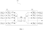
- FIG. 1 illustrates, in a high-level functional block diagram, an example of an analog radio over fiber (AROF) wavelength-division multiplexing (WDM) system 100.
- the AROF WDM system 100 comprises a plurality of transmitters (Tx) 110, a multiplexer (Mux) 120, a demultiplexer (DeMux) 130 and a plurality of receivers 140.
- Radio frequencies (RF in,x ) may be input into the transmitters (Tx x ) 110.
- Each Tx x 110 converts the received RF in,x into an optical signal having a different wavelength ⁇ x for that Tx x 110.
- the optical signals are sent via optical fibers to the multiplexer 120 that combines the signals into a single optical fiber.
- the combined signal is sent a distance via a relatively long optical fiber (typically many kilometers in distance) to the demultiplexer 130 that separates the signals based on their wavelengths ⁇ x and sends the separated signals via several optical fibers to corresponding receivers (Rx x ) 140.
- Each Rx x 140 converts their signal into a RF out,x .
- the transmitters (Tx) 110 may comprise directly modulated laser (DML) diodes.
- the multiplexer 120 and demultiplexer 130 may comprise arrayed waveguide grating (AWG) devices.
- the receivers (Rx) 140 may comprise photodiodes. Transceivers (Tx/Rx) may be used for any Tx 110 or Rx 140.
- Components of the AROF WDM system 100 may be tuned in wavelength.
- the components may be coupled with heating/cooling elements electrically connected to a controller.
- thermal tuning of the Tx 110 may take place by adding or removing heat by a thermoelectric cooler coupled to the Tx 110.
- One may tune the Tx 110 by tuning the refractive index of the laser cavity, or the refractive index of wavelength-selective reflective elements forming the laser cavity, or both.
- each Tx x will be tuned to transmit an optical signal at a desired wavelength ⁇ x .
- it is possible to tune the multiplexer 120 and demultiplexer 130 by using a heating/cooling element coupled to the multiplexer 120 or demultiplexer 130.
- the receivers (Rx) 140 may comprise photodiodes.
- Optical fiber communications typically operate in a wavelength region corresponding to one of several "telecom windows".
- a wavelength range of the optical signal may cover band C and band L recommended by the International Telecommunication Union-Telecommunication Standardization Sector (ITU-T), or any other required wavelength range and wavelength spacing.
- the C band describes one window that is widely used and utilizes wavelengths around 1.5 um (1530-1565 nm). The optical losses of silica fibers are lowest in this region.
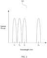
- FIG. 2 schematically illustrates spectral profiles of passbands 200 of ports on a multiplexer 120 in the AROF WDM system 100.
- Each passband has a center wavelength ⁇ x .
- the center wavelengths ⁇ x correspond with an ITU channel.
- the optical signals will not interfere with each other when combined at the multiplexer 120 so that the signals can be separated at the demultiplexer 130.
- each Tx 110 is tuned to emit optical signals having a wavelength equal to the center wavelength of its corresponding passband. This tuning provides optimal optical power. The higher the optical power, the longer the optical signal can travel in the optical fiber without the need for amplification (and thus added cost of an amplifier along the path between the multiplexer 120 and demultiplexer 130).
- FIG. 3 schematically illustrates a spectral profile of a modulated analog radio frequency (RF) signal 300.
- Areas 310 and 320 are regions of distortion of the modulated analog RF signal 300 which comprise a portion of the ACLR.
- Adjacent channel leakage may be caused by many detrimental effects, which may include, for example, back reflection (i.e., due to Rayleigh scattering), four-wave mixing, self-phase modulation (SPM), and Stimulated Brillouin scattering (SBS). Each of these effects may occur in an optical fiber span between the Tx 110 and the Rx 140 in the AROF WDM system 100, causing distortion of the analog RF signal.
- back reflection i.e., due to Rayleigh scattering
- SPM self-phase modulation
- SBS Stimulated Brillouin scattering
- one source of noise which contributes to the degradation of ACLR is the back-reflection of optical power from the optical devices (Tx 110, multiplexer 120, demultiplexer130, Rx 140) and the fiber.
- the light reflected back enters the laser (i.e., one type of Tx 110) and adds to the noise by destabilizing the laser and thus degrading the signal quality.
- sources of back-reflection include the multiplexer120, the demultiplexer130 and the optical fiber. A detrimental effect of back-reflection may be mitigated by using high-isolation optical isolators in each optical link. However, this would be costly on a massive network deployed scale.
- the ACLR may be improved by approximately 3dB to 5dB.
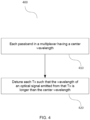
- FIG. 4 illustrates, in a flowchart, an example of a method of reducing ACLR in a radio frequency provide by an AROF WDM system (400), in accordance with an embodiment of the present invention.
- each Tx 110 corresponds to a passband of a port of the multiplexer 120.
- Each passband in the multiplexer 120 has a center wavelength (410) corresponding to an optical channel.
- the controller electrically connected to the AROF WDM system 100 detunes each Tx x 110 such that the wavelength ⁇ ' x of an optical signal emitted from that detuned Tx x 110 is longer than the center wavelength ⁇ x of a corresponding passband in the multiplexer 120 (420).
- the multiplexer 120 (and possibly the demultiplexer 130) is detuned relative to each Tx x 110 such that the center wavelength of each passband in the multiplexer 120 (and demultiplexer 130) is shorter than the the wavelength of an optical signal emitted from a corresponding Tx x .
- the tuning and detuning may be performed thermoelectrically via a controller electrically connected to thermal heating/cooling components in the Tx 110 (or the multiplexer 120/demultiplexer 130 for the alternative detuning step).
- Other steps may be added to the method (400), including monitoring the ACLR in the RF out,x signal, and detuning the demultiplexer, e.g. AWG demultiplexer, to match the detuning of the multiplexer, e.g. AWG multiplexer.
- the detuning in step (420) comprises the controller lowering the optical frequency of optical signals sent by each Tx x 110 such that that each Tx x 110 produces optical signals at optical frequencies that are between 25GHz to 30GHz lower than those corresponding to predetermined optimal center wavelengths ⁇ x (i.e., those corresponding to the center wavelengths ⁇ x of corresponding passbands in the multiplexer 120).
- Lowering the optical frequency by 25GHz to 30GHz is equivalent to increasing the transmission wavelength by approximately 0.2nm to 0.24nm.
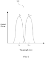
- FIG. 5 schematically illustrates spectral profiles of two passbands where the respective Tx 110 have been detuned to transmit at wavelengths ⁇ ' x and ⁇ ' x+1 .
- ACLR can be reduced.
- each Tx x 110 may be detuned lower by approximately 25GHz to 30GHz, which corresponds to an increase from the corresponding passband central wavelength ⁇ x by 0.2nm to 0.24nm. This level is shown below to be enough to decrease the ACLR by 3dB to 5dB.
- the RF signal used was an analog 20MHz LTE signal at 2.1GHz of RF carrier.
- Sixteen copies of the RF signal were generated with each signal independently modulating a directly modulated laser (DML) (i.e., Tx 110) each.
- DML directly modulated laser
- the center wavelengths of the 16 DML's were tuned to the 100GHz ITU grid from 1549.32nm to 1560.61nm.
- All 16 modulated DML's were multiplexed using an arrayed-waveguide based commercially available multiplexer (i.e., multiplexer 120) and after a 12Km SMF-28e fiber were de-multiplexed with the same (i.e., same type of device used as a multiplexer 120 and demultiplexer 130).
- the multiplexer 120 and demultiplexer 130 have adjacent channel crosstalk of 25dB and non-adjacent channel crosstalk of 30dB.
- Each DML i.e., Tx 110
- each optical signal was detected with an optical detector with 3.5GHz of 3-dB bandwidth and the ACLR was measured with a RF spectrum analyzer.
- FIG. 6 illustrates, in a graph, the observed ACLR as a function of the power received at a reciever (Rx 140).
- FIG. 6 shows that as the received power at the Rx 140 is increased, initially there is an increase in the ACLR as the signal power with respect to relative intensity noise increases. However, after around 4.5dBm of received power, as the received power is increased the non-linear distortions and back-reflection appear to dominate the integrated power in the adjacent channel resulting in a saturation of ACLR and further reduction.
- the AWG multiplexer 120/demultiplexer 130 incur around 1.8dB of ACLR penalty individually (i.e., whether the AWG is used as a multiplexer 120 or as a demultiplexer 130). Both multiplexer 120 and demultiplexer 130 combined together incur 3.6dB of ACLR penalty. This penalty is not attributed to crosstalk since the measurement was performed using a single channel. Thus, the penalty appears to be generated by the reflections from the device.
- Table 1 shows that when the fiber is increased from 12km to 18km, the received power at the optical Rx 140 is decreased by 1.8dB.
- the ACLR degradation is twice that of 12km (i.e., 4.1dB compared to 2.3dB).
- the degradation in ACLR is not linear and should not be attributed to the simple insertion loss.
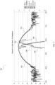
- FIG. 7 illustrates, in a graph, a spectral profile of the multiplexer 120 and demultiplexer 130 channel (710 and 720, respectively) overlaid with received optical power (760), back-reflected optical power (750) and the measured ACLR (730 and 740) for channel 13 (1546.35nm).
- FIG. 7 shows that the maximal received power is achieved when the signal is tuned to the passband center of the multiplexer 120/demultiplexer 130.
- FIGs. 8 and 9 illustrate, in graphs, a spectral profile, or a passband, of the multiplexer 120 and demultiplexer 130 channel (810 and 820, respectively; and 910 and 920, respectively) overlaid with receive optical power (860; 960), back-reflected optical power (850; 950) and the measured ACLR (830; 930) for channels 7 (1541.35nm) and 28 (1558.17nm), respectively.
- receive optical power 860; 960
- back-reflected optical power 850; 950
- the measured ACLR 830; 930
- Both FIGs. 8 and 9 also show an improvement of 3dB in ACLR achieved with detuning.
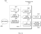
- FIG. 10 is a block diagram of a computing system 1000 that may be used for implementing the devices and methods disclosed herein. Specific devices may utilize all of the components shown or only a subset of the components, and levels of integration may vary from device to device. Furthermore, a device may contain multiple instances of a component, such as multiple processing units, processors, memories, transmitters, receivers, etc.
- the computing system 1000 includes a processing unit 1002.
- the processing unit 1002 includes a central processing unit (CPU) 1014, memory 1008, and may further include a mass storage device 1004, a video adapter 1010, and an I/O interface 1012 connected to a bus 1020.
- CPU central processing unit
- the bus 1020 may be one or more of any type of several bus architectures including a memory bus or memory controller, a peripheral bus, or a video bus.
- the CPU 1014 may comprise any type of electronic data processor.
- the memory 1008 may comprise any type of non-transitory system memory such as static random access memory (SRAM), dynamic random access memory (DRAM), synchronous DRAM (SDRAM), read-only memory (ROM), or a combination thereof.
- SRAM static random access memory
- DRAM dynamic random access memory
- SDRAM synchronous DRAM
- ROM read-only memory
- the memory 1008 may include ROM for use at boot-up, and DRAM for program and data storage for use while executing programs.
- the mass storage 1004 may comprise any type of non-transitory storage device configured to store data, programs, and other information and to make the data, programs, and other information accessible via the bus 1020.
- the mass storage 1004 may comprise, for example, one or more of a solid state drive, hard disk drive, a magnetic disk drive, or an optical disk drive.
- the video adapter 1010 and the I/O interface 1012 provide interfaces to couple external input and output devices to the processing unit 1002.
- input and output devices include a display 1018 coupled to the video adapter 1010 and a mouse/keyboard/printer 1016 coupled to the I/O interface 1012.
- Other devices may be coupled to the processing unit 1002, and additional or fewer interface cards may be utilized.
- a serial interface such as universal serial bus (USB) (not shown) may be used to provide an interface for an external device.
- USB universal serial bus
- the processing unit 1002 may also include one or more network interfaces 1006, which may comprise wired links, such as an Ethernet cable, and/or wireless links to access nodes or different networks.
- the network interfaces 1006 allow the processing unit 1002 to communicate with remote units via the networks.
- the network interfaces 1006 may provide wireless communication via one or more transmitters/transmit antennas and one or more receivers/receive antennas.
- the processing unit 1002 may be coupled to a local-area network 1022 or a wide-area network for data processing and communications with remote devices, such as other processing units, the Internet, or remote storage facilities.
- the present invention may be implemented by using hardware only or by using software and a necessary universal hardware platform. Based on such understandings, the technical solution of the present invention may be embodied in the form of a software product.
- the software product may be stored in a non-volatile or non-transitory storage medium, which can be a compact disk read-only memory (CD-ROM), USB flash disk, or a removable hard disk.
- the software product includes a number of instructions that enable a computer device (personal computer, server, or network device) to execute the methods provided in the embodiments of the present invention. For example, such an execution may correspond to a simulation of the logical operations as described herein.
- the software product may additionally or alternatively include number of instructions that enable a computer device to execute operations for configuring or programming a digital logic apparatus in accordance with embodiments of the present invention.
Landscapes
- Engineering & Computer Science (AREA)
- Physics & Mathematics (AREA)
- Computer Networks & Wireless Communication (AREA)
- Signal Processing (AREA)
- Electromagnetism (AREA)
- General Physics & Mathematics (AREA)
- Optics & Photonics (AREA)
- Nonlinear Science (AREA)
- Condensed Matter Physics & Semiconductors (AREA)
- Microelectronics & Electronic Packaging (AREA)
- Optical Communication System (AREA)
Description
- The present invention pertains to the field of network communications, and in particular to systems and methods for reducing adjacent channel leakage ratio in multichannel communications networks.
- Analog radio over fiber (AROF) is increasingly seen as a viable alternative to conventional digital optical transmission, e.g., the common public radio interface (CPRI), for the next generation wireless systems to directly transmit the analog signal to the antenna. A simple optical detector at the antenna-top converts the analog optical signal into analog electrical signal, to be amplified with a radio frequency (RF) power amplifier (PA) and transmitted into the free space, thereby reducing the complexity of requiring digital to analog conversion circuitry at the antenna top. This methodology, however, puts stringent demands on the optical link in terms of linearity, noise and crosstalk. One such important system parameter dependent on a combination of system linearity, noise and crosstalk is adjacent channel leakage ratio (ACLR). ACLR is defined by the international committee on 3GPP as the ratio of the integrated power in the adjacent channel to the integrated power in the channel of interest.
- This background information is provided to reveal information believed by the applicant to be of possible relevance to the present invention. No admission is necessarily intended, nor should be construed, that any of the preceding information constitutes prior art against the present invention.
-
US 2010/142955 A1 discloses a passive optical network comprisinf: an OLT, an ODN and at least one ONU. The OLT comprises: at least one transmitting unit, which provides one dedicated downstream optical carrier and two dedicated upstream optical carriers for ONU; the two dedicated optical carriers for ONU are configured to carry ONU upstream radio frequency signals; a multiplexing/demultiplexing unit; and at least one receiving unit which obtains the upstream signal from the demultiplexed upstream optical signal. -
US 2009/028552 A1 discloses a system and method using for wavelength monitoring and control in a WDM optical communication system. An aggregate channel monitor detects crosstalk between channels in the aggregate signal. Channel spacing may be modified by an element management system in response to the output of the aggregate channel monitor. - An object of embodiments of the present invention is to provide a method and apparatus for reducing adjacent channel leakage ratio in a multichannel communications network. The present invention is as defined in the appended independent claims.
- In accordance with embodiments of the present invention, there is provided an analog radio over fiber (AROF) wavelength division multiplexing (WDM) system. The AROF WDM system comprises a plurality of transmitters, a multiplexer, a demultiplexer, a plurality of receivers and a controller. Each transmitter is for receiving a radio frequency input signal and for modulating the radio frequency input signal onto an optical signal to obtain a modulated optical signal. The multiplexer is for receiving each modulated optical signal from the plurality of transmitters and for combining the modulated optical signals into a combined optical signal to be sent a distance over an optical fiber. The multiplexer has a pluralities of passbands with each passband having a center wavelength. The demultiplexer is for receiving the combined optical signal and for separating the combined optical signal back into the individual modulated optical signals. Each receiver is for receiving one of the modulated optical signals from the demultiplexer and for converting the received modulated optical signal into a radio frequency output signal. The controller is configured to detune, for each transmitter, one of that transmitter and the multiplexer relative to the other such that a wavelength of the modulated optical signal transmitted by that transmitter is longer than the center wavelength of a corresponding one of the plurality of passbands of the multiplexer.
- In accordance with embodiments of the present invention, there is also provided a method for reducing adjacent channel leakage ratio (ACLR) in a radio frequency signal provided by an analog radio over fiber (AROF) wavelength division multiplexing (WDM) system. The AROF WDM system comprises a plurality of transmitters, a multiplexer having a plurality of passbands with each passband having a center wavelength, a demultiplexer, a plurality of receivers and a controller operably coupled to the plurality of transmitters. The method comprises, for each transmitter, the controller detuning one of that transmitter and the multiplexer relative to the other such that the wavelength of a modulated optical signal transmitted by that transmitter is longer than the center wavelength of a corresponding one of the plurality of passbands of the multiplexer.
- Further features and advantages of the present invention will become apparent from the following detailed description, taken in combination with the appended drawings, in which:
-
FIG. 1 illustrates, in a high-level functional block diagram, an example of an analog radio over fiber (AROF) wavelength division multiplexing (WDM) system; -
FIG. 2 schematically illustrates spectral profiles of optical signals generated by each transmitter in the AROF WDM system; -
FIG. 3 schematically illustrates a spectral profile of a modulated analog radio frequency (RF) signal; -
FIG. 4 illustrates, in a flowchart, an example of a method of improving ACLR in a radio frequency signal provided by an AROF WDM system, in accordance with an embodiment of the present invention; -
FIG. 5 schematically illustrates spectral profiles of two optical signals where the transmitters have been detuned; -
FIG. 6 illustrates, in a graph, the observed ACLR as a function of the power received at a receiver; -
FIG. 7 illustrates, in a graph, a spectral profile of a multiplexer and demultiplexer channel overlaid with received optical power, back-reflected optical power and the measured ACLR forchannel 13; -
FIG. 8 illustrates, in a graph, a spectral profile of the multiplexer and demultiplexer channel overlaid with received optical power, back-reflected optical power and the measured ACLR forchannel 7; -
FIG. 9 , illustrates, in a graph, a spectral profile of the multiplexer and demultiplexer channel overlaid with received optical power, back-reflected optical power and the measured ACLR forchannel 28; and -
FIG. 10 is a block diagram of a computing system that may be used for implementing the devices and methods disclosed herein. - It will be noted that throughout the appended drawings, like features are identified by like reference numerals.
- Embodiments of the present invention are directed towards systems and methods for reducing adjacent channel leakage ratio in multichannel communications networks.
-
FIG. 1 illustrates, in a high-level functional block diagram, an example of an analog radio over fiber (AROF) wavelength-division multiplexing (WDM)system 100. The AROFWDM system 100 comprises a plurality of transmitters (Tx) 110, a multiplexer (Mux) 120, a demultiplexer (DeMux) 130 and a plurality ofreceivers 140. Radio frequencies (RFin,x) may be input into the transmitters (Txx) 110. EachTx x 110 converts the received RFin,x into an optical signal having a different wavelength λx for thatTx x 110. The optical signals are sent via optical fibers to themultiplexer 120 that combines the signals into a single optical fiber. The combined signal is sent a distance via a relatively long optical fiber (typically many kilometers in distance) to thedemultiplexer 130 that separates the signals based on their wavelengths λx and sends the separated signals via several optical fibers to corresponding receivers (Rxx) 140. EachRx x 140 converts their signal into a RFout,x. The transmitters (Tx) 110 may comprise directly modulated laser (DML) diodes. Themultiplexer 120 anddemultiplexer 130 may comprise arrayed waveguide grating (AWG) devices. The receivers (Rx) 140 may comprise photodiodes. Transceivers (Tx/Rx) may be used for anyTx 110 orRx 140. - Components of the AROF
WDM system 100, such as theTx 110, themultiplexer 120, and/or thedemultiplexer 130 may be tuned in wavelength. To that end, the components may be coupled with heating/cooling elements electrically connected to a controller. As is known in the art, thermal tuning of theTx 110 may take place by adding or removing heat by a thermoelectric cooler coupled to theTx 110. One may tune theTx 110 by tuning the refractive index of the laser cavity, or the refractive index of wavelength-selective reflective elements forming the laser cavity, or both. Typically, each Txx will be tuned to transmit an optical signal at a desired wavelength λx. In some embodiments, it is possible to tune themultiplexer 120 anddemultiplexer 130 by using a heating/cooling element coupled to themultiplexer 120 ordemultiplexer 130. The receivers (Rx) 140 may comprise photodiodes. - Optical fiber communications typically operate in a wavelength region corresponding to one of several "telecom windows". A wavelength range of the optical signal may cover band C and band L recommended by the International Telecommunication Union-Telecommunication Standardization Sector (ITU-T), or any other required wavelength range and wavelength spacing. The C band describes one window that is widely used and utilizes wavelengths around 1.5 um (1530-1565 nm). The optical losses of silica fibers are lowest in this region.
-
FIG. 2 schematically illustrates spectral profiles ofpassbands 200 of ports on amultiplexer 120 in theAROF WDM system 100. Each passband has a center wavelength λx. Typically, the center wavelengths λx correspond with an ITU channel. As long as the wavelengths λx are sufficiently spaced apart, the optical signals will not interfere with each other when combined at themultiplexer 120 so that the signals can be separated at thedemultiplexer 130. In typical uses of the AROF WDM system, eachTx 110 is tuned to emit optical signals having a wavelength equal to the center wavelength of its corresponding passband. This tuning provides optimal optical power. The higher the optical power, the longer the optical signal can travel in the optical fiber without the need for amplification (and thus added cost of an amplifier along the path between themultiplexer 120 and demultiplexer 130). -
FIG. 3 schematically illustrates a spectral profile of a modulated analog radio frequency (RF)signal 300.Areas Tx 110 and theRx 140 in theAROF WDM system 100, causing distortion of the analog RF signal. - As noted above, one source of noise which contributes to the degradation of ACLR is the back-reflection of optical power from the optical devices (
Tx 110,multiplexer 120, demultiplexer130, Rx 140) and the fiber. The light reflected back enters the laser (i.e., one type of Tx 110) and adds to the noise by destabilizing the laser and thus degrading the signal quality. In an AROF WDM system, sources of back-reflection include the multiplexer120, the demultiplexer130 and the optical fiber. A detrimental effect of back-reflection may be mitigated by using high-isolation optical isolators in each optical link. However, this would be costly on a massive network deployed scale. - As will be discussed below, by detuning (i.e., lowering) the
Tx 110 optical frequency away from amultiplexer 120/demultiplexer 130 (such as an AWG) by approximately 25GHz to 30GHz (i.e., detuning the laser wavelength such that it is longer than the central wavelength of a corresponding passband in themultiplexer 120 by a relatively small amount), the ACLR may be improved by approximately 3dB to 5dB. -
FIG. 4 illustrates, in a flowchart, an example of a method of reducing ACLR in a radio frequency provide by an AROF WDM system (400), in accordance with an embodiment of the present invention. As is noted above, in anAROF WDM system 100, eachTx 110 corresponds to a passband of a port of themultiplexer 120. Each passband in themultiplexer 120 has a center wavelength (410) corresponding to an optical channel. The controller electrically connected to theAROF WDM system 100 detunes eachTx x 110 such that the wavelength λ'x of an optical signal emitted from that detunedTx x 110 is longer than the center wavelength λx of a corresponding passband in the multiplexer 120 (420). Alternatively, the multiplexer 120 (and possibly the demultiplexer 130) is detuned relative to eachTx x 110 such that the center wavelength of each passband in the multiplexer 120 (and demultiplexer 130) is shorter than the the wavelength of an optical signal emitted from a corresponding Txx. The tuning and detuning may be performed thermoelectrically via a controller electrically connected to thermal heating/cooling components in the Tx 110 (or themultiplexer 120/demultiplexer 130 for the alternative detuning step). Other steps may be added to the method (400), including monitoring the ACLR in the RFout,x signal, and detuning the demultiplexer, e.g. AWG demultiplexer, to match the detuning of the multiplexer, e.g. AWG multiplexer. - As will be discussed below, the detuning in step (420) comprises the controller lowering the optical frequency of optical signals sent by each
Tx x 110 such that that eachTx x 110 produces optical signals at optical frequencies that are between 25GHz to 30GHz lower than those corresponding to predetermined optimal center wavelengths λx (i.e., those corresponding to the center wavelengths λx of corresponding passbands in the multiplexer 120). Lowering the optical frequency by 25GHz to 30GHz is equivalent to increasing the transmission wavelength by approximately 0.2nm to 0.24nm. -
FIG. 5 schematically illustrates spectral profiles of two passbands where therespective Tx 110 have been detuned to transmit at wavelengths λ' x and λ' x+1. By detuning theTx 110, ACLR can be reduced. As was noted above, eachTx x 110 may be detuned lower by approximately 25GHz to 30GHz, which corresponds to an increase from the corresponding passband central wavelength λx by 0.2nm to 0.24nm. This level is shown below to be enough to decrease the ACLR by 3dB to 5dB. - To demonstrate ACLR reduction, an experiment was set up using an AROF WDM system similar to the
AROF WDM system 100 inFIG. 1 . In the experiment, the RF signal used was an analog 20MHz LTE signal at 2.1GHz of RF carrier. Sixteen copies of the RF signal were generated with each signal independently modulating a directly modulated laser (DML) (i.e., Tx 110) each. The center wavelengths of the 16 DML's were tuned to the 100GHz ITU grid from 1549.32nm to 1560.61nm. All 16 modulated DML's were multiplexed using an arrayed-waveguide based commercially available multiplexer (i.e., multiplexer 120) and after a 12Km SMF-28e fiber were de-multiplexed with the same (i.e., same type of device used as amultiplexer 120 and demultiplexer 130). Themultiplexer 120 anddemultiplexer 130 have adjacent channel crosstalk of 25dB and non-adjacent channel crosstalk of 30dB. Each DML (i.e., Tx 110) is transmitting 10 to 12dBm optical power per channel. After transmission and demultiplexing each optical signal was detected with an optical detector with 3.5GHz of 3-dB bandwidth and the ACLR was measured with a RF spectrum analyzer. - To isolate possible causes of the performance degradation of each optical block, a detailed characterization for the single-channel case was carried out at Channel-7 (1541.35nm) without any WDM neighbors. This provided insight into the penalty which each block (i.e.,
optical multiplexer 120,optical demultiplexer 130 and fiber) contributes to the overall performance. DML (Tx 110) output optical power was 12dBm and the received power at the optical receiver (Rx 140) was varied with an optical attenuator. -
FIG. 6 illustrates, in a graph, the observed ACLR as a function of the power received at a reciever (Rx 140).FIG. 6 shows that as the received power at theRx 140 is increased, initially there is an increase in the ACLR as the signal power with respect to relative intensity noise increases. However, after around 4.5dBm of received power, as the received power is increased the non-linear distortions and back-reflection appear to dominate the integrated power in the adjacent channel resulting in a saturation of ACLR and further reduction. TheAWG multiplexer 120/demultiplexer 130 incur around 1.8dB of ACLR penalty individually (i.e., whether the AWG is used as amultiplexer 120 or as a demultiplexer 130). Bothmultiplexer 120 anddemultiplexer 130 combined together incur 3.6dB of ACLR penalty. This penalty is not attributed to crosstalk since the measurement was performed using a single channel. Thus, the penalty appears to be generated by the reflections from the device. - The SMF-28e fiber was available in three spools of 6km each. As each additional spool is inserted into the link it incurs its own insertion loss (i.e., 0.2dB/km x 6km = 1.2dB) as well as enhances the fiber non-linear effect. Table 1 below shows that when the fiber is increased from 12km to 18km, the received power at the
optical Rx 140 is decreased by 1.8dB. However, the ACLR degradation is twice that of 12km (i.e., 4.1dB compared to 2.3dB). Thus, the degradation in ACLR is not linear and should not be attributed to the simple insertion loss. This suggests that the combined effect of Rayleigh and Stimulated Brillouin scattering (SBS) as well as self-phase modulation (SPM) in the fiber causes the additional penalty.Table 1: ACLR penalty of Fiber Fiber length ACLR degradation [dB] Received Optical Power [dBm] Added Insertion Loss [dB] 6km 5.2 12km 2.3 3.9 1.3 18km 4.1 2.3 1.6 - The single-channel results suggest that at the optimal received power of 4.5dBm power, the ACLR is maximized. However, with the
multiplexer 120, fiber anddemultiplexer 130 in the link, the optimal ACLR and the maximal received power do not correlate.FIG. 7 illustrates, in a graph, a spectral profile of themultiplexer 120 anddemultiplexer 130 channel (710 and 720, respectively) overlaid with received optical power (760), back-reflected optical power (750) and the measured ACLR (730 and 740) for channel 13 (1546.35nm).FIG. 7 shows that the maximal received power is achieved when the signal is tuned to the passband center of themultiplexer 120/demultiplexer 130. However, as the signal is detuned away from the center towards the red side of the passband (i.e., increase in wavelength), an improvement of up to 3dB to 5dB occurs in the ACLR. This improvement may be attributed to the reduction of back-reflection which was measured and is plotted inFIG. 7 at 750.FIGs. 8 and9 , illustrate, in graphs, a spectral profile, or a passband, of themultiplexer 120 anddemultiplexer 130 channel (810 and 820, respectively; and 910 and 920, respectively) overlaid with receive optical power (860; 960), back-reflected optical power (850; 950) and the measured ACLR (830; 930) for channels 7 (1541.35nm) and 28 (1558.17nm), respectively. BothFIGs. 8 and9 also show an improvement of 3dB in ACLR achieved with detuning. -
FIG. 10 is a block diagram of acomputing system 1000 that may be used for implementing the devices and methods disclosed herein. Specific devices may utilize all of the components shown or only a subset of the components, and levels of integration may vary from device to device. Furthermore, a device may contain multiple instances of a component, such as multiple processing units, processors, memories, transmitters, receivers, etc. Thecomputing system 1000 includes aprocessing unit 1002. Theprocessing unit 1002 includes a central processing unit (CPU) 1014,memory 1008, and may further include amass storage device 1004, avideo adapter 1010, and an I/O interface 1012 connected to abus 1020. - The
bus 1020 may be one or more of any type of several bus architectures including a memory bus or memory controller, a peripheral bus, or a video bus. TheCPU 1014 may comprise any type of electronic data processor. Thememory 1008 may comprise any type of non-transitory system memory such as static random access memory (SRAM), dynamic random access memory (DRAM), synchronous DRAM (SDRAM), read-only memory (ROM), or a combination thereof. Thememory 1008 may include ROM for use at boot-up, and DRAM for program and data storage for use while executing programs. - The
mass storage 1004 may comprise any type of non-transitory storage device configured to store data, programs, and other information and to make the data, programs, and other information accessible via thebus 1020. Themass storage 1004 may comprise, for example, one or more of a solid state drive, hard disk drive, a magnetic disk drive, or an optical disk drive. - The
video adapter 1010 and the I/O interface 1012 provide interfaces to couple external input and output devices to theprocessing unit 1002. As illustrated, examples of input and output devices include adisplay 1018 coupled to thevideo adapter 1010 and a mouse/keyboard/printer 1016 coupled to the I/O interface 1012. Other devices may be coupled to theprocessing unit 1002, and additional or fewer interface cards may be utilized. For example, a serial interface such as universal serial bus (USB) (not shown) may be used to provide an interface for an external device. - The
processing unit 1002 may also include one ormore network interfaces 1006, which may comprise wired links, such as an Ethernet cable, and/or wireless links to access nodes or different networks. The network interfaces 1006 allow theprocessing unit 1002 to communicate with remote units via the networks. For example, thenetwork interfaces 1006 may provide wireless communication via one or more transmitters/transmit antennas and one or more receivers/receive antennas. Theprocessing unit 1002 may be coupled to a local-area network 1022 or a wide-area network for data processing and communications with remote devices, such as other processing units, the Internet, or remote storage facilities. - Unless defined otherwise, all technical and scientific terms used herein have the same meaning as commonly understood by one of ordinary skill in the art to which this invention belongs.
- Through the descriptions of the preceding embodiments, the present invention may be implemented by using hardware only or by using software and a necessary universal hardware platform. Based on such understandings, the technical solution of the present invention may be embodied in the form of a software product. The software product may be stored in a non-volatile or non-transitory storage medium, which can be a compact disk read-only memory (CD-ROM), USB flash disk, or a removable hard disk. The software product includes a number of instructions that enable a computer device (personal computer, server, or network device) to execute the methods provided in the embodiments of the present invention. For example, such an execution may correspond to a simulation of the logical operations as described herein. The software product may additionally or alternatively include number of instructions that enable a computer device to execute operations for configuring or programming a digital logic apparatus in accordance with embodiments of the present invention.
- Although the present invention has been described with reference to specific features and embodiments thereof, it is evident that various modifications and combinations can be made thereto without departing from the invention. The specification and drawings are, accordingly, to be regarded simply as an illustration of the invention as defined by the appended claims, and are contemplated to cover any and all modifications, variations, combinations or equivalents that fall within the scope of the present invention.
Claims (11)
- An analog radio over fiber (AROF) wavelength division multiplexing (WDM) system comprising:a plurality of transmitters (110), each transmitter (110) for receiving a radio frequency input signal and for modulating the radio frequency input signal onto an optical signal to obtain a modulated optical signal;a multiplexer (120) for receiving each modulated optical signal from the plurality of transmitters (110) and for combining the modulated optical signals into a combined optical signal, the multiplexer (120) having a plurality of passbands, each passband having a center wavelength;a demultiplexer (130) for receiving the combined optical signal and for separating the combined optical signal back into the individual modulated optical signals; anda plurality of receivers (140), each receiver (140) for receiving one of the modulated optical signals from the demultiplexer (130) and for converting the received modulated optical signal into a radio frequency output signal;characterized bya controller configured to detune each transmitter (110), or detune the multiplexer (120) relative to each transmitter (110), such that a wavelength of the modulated optical signal transmitted by that transmitter is longer than the center wavelength of a corresponding one of the plurality of passbands of the multiplexer;wherein the controller is configured to detune each transmitter (110), or detune the multiplexer (120) relative to each transmitter (110), such that that transmitter produces the modulated optical signal at an optical frequency that is between 25GHz and 30GHz lower than a center optical frequency of the corresponding passband of the multiplexer (120);or the controller is configured to detune each transmitter (110), or detune the multiplexer (120) relative to each transmitter (110), such that that transmitter produces the modulated optical signal at a wavelength that is 0.2 nanometers to 0.24 nanometers longer than the center wavelength of the corresponding passband of the multiplexer (120).
- The AROF WDM system as claimed in claim 1, wherein the controller is further configured to detune each transmitter off of the center wavelength of the corresponding passband of the multiplexer (120).
- The AROF WDM system as claimed in claim 1 or claim 2, wherein the controller is further configured to detune the multiplexer (120) such that the modulated optical signal transmitted by each transmitter (110) has a wavelength that is longer than the center wavelength of the corresponding passband of the multiplexer (120).
- The AROF WDM system as claimed in any one of claim 1 to claim 3, wherein each transmitter (110) comprises a directly modulated laser diode.
- The AROF WDM system as claimed in claim 4, wherein each transmitter (110) further comprises a thermoelectric cooler, wherein, to detune the transmitters, the controller is configured to lower the temperature of the directly modulated laser diode using a corresponding thermoelectric cooler.
- A method characterized for reducing adjacent channel leakage ratio (ACLR) in a radio frequency signal provided by an analog radio over fiber (AROF) wavelength division multiplexing (WDM) system comprising a plurality of transmitters (110), a multiplexer (120) having a plurality of passbands with each passband having a center wavelength, a demultiplexer (130), a plurality of receivers (140) and a controller operably coupled to the plurality of transmitters, the method comprising, the controller detuning each transmitter (110) or the multiplexer (120) relative to each transmitter (110) such that the wavelength of a modulated optical signal transmitted by that transmitter is longer than the center wavelength of a corresponding one of the plurality of passbands of the multiplexer;wherein the detuning comprises the controller lowering the optical frequency of a modulated optical signal sent by each transmitter to a value lower by 25GHz to 30GHz than a center optical frequency of the corresponding passband of the multiplexer;or the detuning comprises the controller detuning each transmitter or the multiplexer such that that transmitter produces a modulated optical signal at a wavelength that is 0.2 nanometers to 0.24 nanometers longer than a center wavelength of the corresponding passband of the multiplexer.
- The method as claimed in claim 6, wherein the detuning comprises the controller detuning each transmitter off of the center wavelength of the corresponding passband of the multiplexer.
- The method as claimed in claim 6 or claim 7, wherein the detuning comprises the controller detuning the multiplexer such that a modulated optical signal transmitted by each transmitter has a wavelength that is longer than the center wavelength of the corresponding passband of the multiplexer.
- The method as claimed in any one of claim 6 to claim 8, wherein each transmitter comprises a laser diode, wherein the detuning comprises, for each transmitter, the controller lowering temperature of the laser diode of that transmitter.
- The method as claimed in any one of claim 6 to claim 9, further comprising monitoring ACLR in the AROF WDM system.
- The method as claimed in claim 8, wherein the multiplexer comprises an arrayed waveguide grating (AWG) multiplexer, wherein the detuning comprises changing temperature of the AWG multiplexer.
Applications Claiming Priority (2)
| Application Number | Priority Date | Filing Date | Title |
|---|---|---|---|
| US15/366,125 US10097268B2 (en) | 2016-12-01 | 2016-12-01 | Systems and methods for reducing adjacent channel leakage ratio |
| PCT/CN2017/112118 WO2018099300A1 (en) | 2016-12-01 | 2017-11-21 | Systems and methods for reducing adjacent channel leakage ratio |
Publications (3)
| Publication Number | Publication Date |
|---|---|
| EP3420652A1 EP3420652A1 (en) | 2019-01-02 |
| EP3420652A4 EP3420652A4 (en) | 2019-03-20 |
| EP3420652B1 true EP3420652B1 (en) | 2024-08-21 |
Family
ID=62241191
Family Applications (1)
| Application Number | Title | Priority Date | Filing Date |
|---|---|---|---|
| EP17876421.3A Active EP3420652B1 (en) | 2016-12-01 | 2017-11-21 | Systems and methods for reducing adjacent channel leakage ratio |
Country Status (5)
| Country | Link |
|---|---|
| US (1) | US10097268B2 (en) |
| EP (1) | EP3420652B1 (en) |
| JP (1) | JP6823077B2 (en) |
| CN (1) | CN108781117B (en) |
| WO (1) | WO2018099300A1 (en) |
Families Citing this family (7)
| Publication number | Priority date | Publication date | Assignee | Title |
|---|---|---|---|---|
| WO2018013756A1 (en) * | 2016-07-15 | 2018-01-18 | Safe-Com Wireless | A method, apparatus and system to amplify and transport analog signals |
| US10439720B2 (en) | 2017-05-19 | 2019-10-08 | Adolite Inc. | FPC-based optical interconnect module on glass interposer |
| US10629161B2 (en) * | 2017-08-28 | 2020-04-21 | National Instruments Corporation | Automatic multi-clock circuit generation |
| JP6741365B2 (en) * | 2018-03-20 | 2020-08-19 | 三菱電機株式会社 | Optical signal control device and optical communication system |
| DE102021201022A1 (en) | 2021-02-04 | 2022-08-04 | Robert Bosch Gesellschaft mit beschränkter Haftung | Optical phase shifter |
| JP2024539460A (en) * | 2021-11-20 | 2024-10-28 | オーエフエス ファイテル,エルエルシー | Enhanced backscatter optical fiber network |
| CN116155383A (en) * | 2023-01-13 | 2023-05-23 | 讯芸电子科技(中山)有限公司 | Single Fiber Multitasking Transmission System |
Family Cites Families (16)
| Publication number | Priority date | Publication date | Assignee | Title |
|---|---|---|---|---|
| JPH11205240A (en) * | 1998-01-08 | 1999-07-30 | Toshiba Corp | Optical transmission equipment |
| US6509987B1 (en) | 1999-08-10 | 2003-01-21 | Lucent Technologies | Channel band conversion apparatus for optical transmission systems |
| JP2002158639A (en) * | 2000-11-20 | 2002-05-31 | Toshiba Corp | Optical transmitter and wavelength multiplexing optical transmitter |
| JP2003051786A (en) * | 2001-08-06 | 2003-02-21 | Fujitsu Ltd | WDM optical transmission equipment |
| JP2002305507A (en) * | 2002-01-28 | 2002-10-18 | Toshiba Corp | Optical communication device |
| JP2006527573A (en) * | 2003-06-13 | 2006-11-30 | 松下電器産業株式会社 | Optical transmission system that controls gain to reduce spurious signal components |
| KR100744372B1 (en) * | 2005-02-17 | 2007-07-30 | 삼성전자주식회사 | Passive / Wireless Integrated Wavelength Division Multiplexing Optical Subscriber Network Device Using Wavelength Locked Light Source |
| US7778550B2 (en) * | 2007-07-27 | 2010-08-17 | Tyco Electronics Subsea Communications Llc | System and method for wavelength monitoring and control |
| CN101399618B (en) * | 2007-09-26 | 2011-06-15 | 华为技术有限公司 | Optical line terminal, passive optical network and radio frequency signal transmission method |
| CN101272214B (en) | 2008-04-30 | 2011-09-07 | 华中科技大学 | Transmission control method of wavelength division multiplexing system |
| US8437637B2 (en) * | 2010-11-29 | 2013-05-07 | The Chinese University Of Hong Kong | Methods and systems for multicast control |
| US8606110B2 (en) * | 2012-01-08 | 2013-12-10 | Optiway Ltd. | Optical distributed antenna system |
| CN103650380B (en) | 2013-07-19 | 2016-05-25 | 华为技术有限公司 | The crosstalk method and apparatus of cost of a kind of attenuating |
| CN103560833A (en) * | 2013-08-16 | 2014-02-05 | 北京邮电大学 | Method for restraining SRS crosstalk in optical access network |
| CN103780308B (en) * | 2014-01-13 | 2017-01-25 | 电子科技大学 | Multi-wavelength all-optical regenerative device capable of inhibiting crosstalk and method thereof |
| US9746746B2 (en) * | 2014-08-01 | 2017-08-29 | Mohammad A Mazed | Fast optical switch and its applications in optical communication |
-
2016
- 2016-12-01 US US15/366,125 patent/US10097268B2/en active Active
-
2017
- 2017-11-21 WO PCT/CN2017/112118 patent/WO2018099300A1/en not_active Ceased
- 2017-11-21 CN CN201780014791.5A patent/CN108781117B/en active Active
- 2017-11-21 JP JP2018554506A patent/JP6823077B2/en active Active
- 2017-11-21 EP EP17876421.3A patent/EP3420652B1/en active Active
Also Published As
| Publication number | Publication date |
|---|---|
| EP3420652A4 (en) | 2019-03-20 |
| JP2019516306A (en) | 2019-06-13 |
| US20180159627A1 (en) | 2018-06-07 |
| WO2018099300A1 (en) | 2018-06-07 |
| CN108781117A (en) | 2018-11-09 |
| CN108781117B (en) | 2020-06-02 |
| JP6823077B2 (en) | 2021-01-27 |
| US10097268B2 (en) | 2018-10-09 |
| EP3420652A1 (en) | 2019-01-02 |
Similar Documents
| Publication | Publication Date | Title |
|---|---|---|
| US10097268B2 (en) | Systems and methods for reducing adjacent channel leakage ratio | |
| US9219565B2 (en) | Optical transmission apparatus and dummy light inserting method | |
| Zirngibl et al. | Digitally tunable channel dropping filter/equalizer based on waveguide grating router and optical amplifier integration | |
| US7831118B2 (en) | Coarse wavelength division multiplexing optical transmission system, and coarse wavelength division multiplexing optical transmission method | |
| US10404366B2 (en) | Optical signal monitor, optical wavelength multiplexing transmitter, and method for monitoring optical signal | |
| KR101600014B1 (en) | Wavelength division multiplexing passive optical network and optical output signal performance measuring method for the network | |
| US9485026B2 (en) | Scheme for remote control of the wavelength of a tunable transmitter in a smart transceiver | |
| JPH11331127A (en) | Wavelength division multiplexing system and its terminal station | |
| US7203392B2 (en) | Optical apparatus for bidirectional optical communication | |
| US8867922B2 (en) | Control device of node transferring signal light | |
| Presi et al. | Uncooled and polarization independent operation of self-seeded Fabry–Pérot lasers for WDM-PONs | |
| WO2022199277A1 (en) | Power compensation method and apparatus, and communication system | |
| US7054058B2 (en) | Pumping source having a number of pump lasers for Raman amplification of a WDM signal with the aid of minimized four-wave mixing | |
| US9124382B2 (en) | Transmission device, transmission system, and method for adjusting passband | |
| US6970613B2 (en) | Optical receiver and optical transmission apparatus | |
| Tomkos | Transport performance of WDM metropolitan area transparent optical networks | |
| KR100594961B1 (en) | Optical communication device using subcarrier multiple access method and method | |
| EP3289704B1 (en) | Optical receiver and method of receiving an optical communications signal | |
| EP3158665B1 (en) | An optical device, an optical transceiver and a network node | |
| US20240106560A1 (en) | Wavelength conversion device and optical transmission system | |
| JP6135068B2 (en) | Optical transmission system, optical amplifier for relay, and optical transmission method | |
| JPH11252050A (en) | Wavelength division multiplexing type optical transmission system |
Legal Events
| Date | Code | Title | Description |
|---|---|---|---|
| STAA | Information on the status of an ep patent application or granted ep patent |
Free format text: STATUS: THE INTERNATIONAL PUBLICATION HAS BEEN MADE |
|
| PUAI | Public reference made under article 153(3) epc to a published international application that has entered the european phase |
Free format text: ORIGINAL CODE: 0009012 |
|
| STAA | Information on the status of an ep patent application or granted ep patent |
Free format text: STATUS: REQUEST FOR EXAMINATION WAS MADE |
|
| 17P | Request for examination filed |
Effective date: 20180925 |
|
| AK | Designated contracting states |
Kind code of ref document: A1 Designated state(s): AL AT BE BG CH CY CZ DE DK EE ES FI FR GB GR HR HU IE IS IT LI LT LU LV MC MK MT NL NO PL PT RO RS SE SI SK SM TR |
|
| AX | Request for extension of the european patent |
Extension state: BA ME |
|
| A4 | Supplementary search report drawn up and despatched |
Effective date: 20190214 |
|
| RIC1 | Information provided on ipc code assigned before grant |
Ipc: H04J 14/02 20060101ALI20190208BHEP Ipc: H04B 10/572 20130101AFI20190208BHEP Ipc: H04B 10/2575 20130101ALI20190208BHEP Ipc: H04B 10/2543 20130101ALI20190208BHEP Ipc: H04B 10/2507 20130101ALI20190208BHEP |
|
| DAV | Request for validation of the european patent (deleted) | ||
| DAX | Request for extension of the european patent (deleted) | ||
| STAA | Information on the status of an ep patent application or granted ep patent |
Free format text: STATUS: EXAMINATION IS IN PROGRESS |
|
| 17Q | First examination report despatched |
Effective date: 20210830 |
|
| GRAP | Despatch of communication of intention to grant a patent |
Free format text: ORIGINAL CODE: EPIDOSNIGR1 |
|
| STAA | Information on the status of an ep patent application or granted ep patent |
Free format text: STATUS: GRANT OF PATENT IS INTENDED |
|
| INTG | Intention to grant announced |
Effective date: 20240417 |
|
| GRAS | Grant fee paid |
Free format text: ORIGINAL CODE: EPIDOSNIGR3 |
|
| GRAA | (expected) grant |
Free format text: ORIGINAL CODE: 0009210 |
|
| STAA | Information on the status of an ep patent application or granted ep patent |
Free format text: STATUS: THE PATENT HAS BEEN GRANTED |
|
| AK | Designated contracting states |
Kind code of ref document: B1 Designated state(s): AL AT BE BG CH CY CZ DE DK EE ES FI FR GB GR HR HU IE IS IT LI LT LU LV MC MK MT NL NO PL PT RO RS SE SI SK SM TR |
|
| REG | Reference to a national code |
Ref country code: GB Ref legal event code: FG4D |
|
| REG | Reference to a national code |
Ref country code: CH Ref legal event code: EP |
|
| REG | Reference to a national code |
Ref country code: IE Ref legal event code: FG4D |
|
| REG | Reference to a national code |
Ref country code: DE Ref legal event code: R096 Ref document number: 602017084335 Country of ref document: DE |
|
| REG | Reference to a national code |
Ref country code: LT Ref legal event code: MG9D |
|
| REG | Reference to a national code |
Ref country code: NL Ref legal event code: MP Effective date: 20240821 |
|
| PG25 | Lapsed in a contracting state [announced via postgrant information from national office to epo] |
Ref country code: NO Free format text: LAPSE BECAUSE OF FAILURE TO SUBMIT A TRANSLATION OF THE DESCRIPTION OR TO PAY THE FEE WITHIN THE PRESCRIBED TIME-LIMIT Effective date: 20241121 |
|
| REG | Reference to a national code |
Ref country code: AT Ref legal event code: MK05 Ref document number: 1716547 Country of ref document: AT Kind code of ref document: T Effective date: 20240821 |
|
| PG25 | Lapsed in a contracting state [announced via postgrant information from national office to epo] |
Ref country code: NL Free format text: LAPSE BECAUSE OF FAILURE TO SUBMIT A TRANSLATION OF THE DESCRIPTION OR TO PAY THE FEE WITHIN THE PRESCRIBED TIME-LIMIT Effective date: 20240821 Ref country code: PL Free format text: LAPSE BECAUSE OF FAILURE TO SUBMIT A TRANSLATION OF THE DESCRIPTION OR TO PAY THE FEE WITHIN THE PRESCRIBED TIME-LIMIT Effective date: 20240821 Ref country code: PT Free format text: LAPSE BECAUSE OF FAILURE TO SUBMIT A TRANSLATION OF THE DESCRIPTION OR TO PAY THE FEE WITHIN THE PRESCRIBED TIME-LIMIT Effective date: 20241223 Ref country code: GR Free format text: LAPSE BECAUSE OF FAILURE TO SUBMIT A TRANSLATION OF THE DESCRIPTION OR TO PAY THE FEE WITHIN THE PRESCRIBED TIME-LIMIT Effective date: 20241122 Ref country code: FI Free format text: LAPSE BECAUSE OF FAILURE TO SUBMIT A TRANSLATION OF THE DESCRIPTION OR TO PAY THE FEE WITHIN THE PRESCRIBED TIME-LIMIT Effective date: 20240821 |
|
| PG25 | Lapsed in a contracting state [announced via postgrant information from national office to epo] |
Ref country code: BG Free format text: LAPSE BECAUSE OF FAILURE TO SUBMIT A TRANSLATION OF THE DESCRIPTION OR TO PAY THE FEE WITHIN THE PRESCRIBED TIME-LIMIT Effective date: 20240821 |
|
| PG25 | Lapsed in a contracting state [announced via postgrant information from national office to epo] |
Ref country code: LV Free format text: LAPSE BECAUSE OF FAILURE TO SUBMIT A TRANSLATION OF THE DESCRIPTION OR TO PAY THE FEE WITHIN THE PRESCRIBED TIME-LIMIT Effective date: 20240821 |
|
| PG25 | Lapsed in a contracting state [announced via postgrant information from national office to epo] |
Ref country code: IS Free format text: LAPSE BECAUSE OF FAILURE TO SUBMIT A TRANSLATION OF THE DESCRIPTION OR TO PAY THE FEE WITHIN THE PRESCRIBED TIME-LIMIT Effective date: 20241221 Ref country code: AT Free format text: LAPSE BECAUSE OF FAILURE TO SUBMIT A TRANSLATION OF THE DESCRIPTION OR TO PAY THE FEE WITHIN THE PRESCRIBED TIME-LIMIT Effective date: 20240821 |
|
| PG25 | Lapsed in a contracting state [announced via postgrant information from national office to epo] |
Ref country code: HR Free format text: LAPSE BECAUSE OF FAILURE TO SUBMIT A TRANSLATION OF THE DESCRIPTION OR TO PAY THE FEE WITHIN THE PRESCRIBED TIME-LIMIT Effective date: 20240821 |
|
| PG25 | Lapsed in a contracting state [announced via postgrant information from national office to epo] |
Ref country code: ES Free format text: LAPSE BECAUSE OF FAILURE TO SUBMIT A TRANSLATION OF THE DESCRIPTION OR TO PAY THE FEE WITHIN THE PRESCRIBED TIME-LIMIT Effective date: 20240821 Ref country code: RS Free format text: LAPSE BECAUSE OF FAILURE TO SUBMIT A TRANSLATION OF THE DESCRIPTION OR TO PAY THE FEE WITHIN THE PRESCRIBED TIME-LIMIT Effective date: 20241121 |
|
| PG25 | Lapsed in a contracting state [announced via postgrant information from national office to epo] |
Ref country code: RS Free format text: LAPSE BECAUSE OF FAILURE TO SUBMIT A TRANSLATION OF THE DESCRIPTION OR TO PAY THE FEE WITHIN THE PRESCRIBED TIME-LIMIT Effective date: 20241121 Ref country code: PT Free format text: LAPSE BECAUSE OF FAILURE TO SUBMIT A TRANSLATION OF THE DESCRIPTION OR TO PAY THE FEE WITHIN THE PRESCRIBED TIME-LIMIT Effective date: 20241223 Ref country code: PL Free format text: LAPSE BECAUSE OF FAILURE TO SUBMIT A TRANSLATION OF THE DESCRIPTION OR TO PAY THE FEE WITHIN THE PRESCRIBED TIME-LIMIT Effective date: 20240821 Ref country code: NO Free format text: LAPSE BECAUSE OF FAILURE TO SUBMIT A TRANSLATION OF THE DESCRIPTION OR TO PAY THE FEE WITHIN THE PRESCRIBED TIME-LIMIT Effective date: 20241121 Ref country code: NL Free format text: LAPSE BECAUSE OF FAILURE TO SUBMIT A TRANSLATION OF THE DESCRIPTION OR TO PAY THE FEE WITHIN THE PRESCRIBED TIME-LIMIT Effective date: 20240821 Ref country code: LV Free format text: LAPSE BECAUSE OF FAILURE TO SUBMIT A TRANSLATION OF THE DESCRIPTION OR TO PAY THE FEE WITHIN THE PRESCRIBED TIME-LIMIT Effective date: 20240821 Ref country code: IS Free format text: LAPSE BECAUSE OF FAILURE TO SUBMIT A TRANSLATION OF THE DESCRIPTION OR TO PAY THE FEE WITHIN THE PRESCRIBED TIME-LIMIT Effective date: 20241221 Ref country code: HR Free format text: LAPSE BECAUSE OF FAILURE TO SUBMIT A TRANSLATION OF THE DESCRIPTION OR TO PAY THE FEE WITHIN THE PRESCRIBED TIME-LIMIT Effective date: 20240821 Ref country code: GR Free format text: LAPSE BECAUSE OF FAILURE TO SUBMIT A TRANSLATION OF THE DESCRIPTION OR TO PAY THE FEE WITHIN THE PRESCRIBED TIME-LIMIT Effective date: 20241122 Ref country code: FI Free format text: LAPSE BECAUSE OF FAILURE TO SUBMIT A TRANSLATION OF THE DESCRIPTION OR TO PAY THE FEE WITHIN THE PRESCRIBED TIME-LIMIT Effective date: 20240821 Ref country code: ES Free format text: LAPSE BECAUSE OF FAILURE TO SUBMIT A TRANSLATION OF THE DESCRIPTION OR TO PAY THE FEE WITHIN THE PRESCRIBED TIME-LIMIT Effective date: 20240821 Ref country code: BG Free format text: LAPSE BECAUSE OF FAILURE TO SUBMIT A TRANSLATION OF THE DESCRIPTION OR TO PAY THE FEE WITHIN THE PRESCRIBED TIME-LIMIT Effective date: 20240821 Ref country code: AT Free format text: LAPSE BECAUSE OF FAILURE TO SUBMIT A TRANSLATION OF THE DESCRIPTION OR TO PAY THE FEE WITHIN THE PRESCRIBED TIME-LIMIT Effective date: 20240821 |
|
| PG25 | Lapsed in a contracting state [announced via postgrant information from national office to epo] |
Ref country code: RO Free format text: LAPSE BECAUSE OF FAILURE TO SUBMIT A TRANSLATION OF THE DESCRIPTION OR TO PAY THE FEE WITHIN THE PRESCRIBED TIME-LIMIT Effective date: 20240821 Ref country code: SM Free format text: LAPSE BECAUSE OF FAILURE TO SUBMIT A TRANSLATION OF THE DESCRIPTION OR TO PAY THE FEE WITHIN THE PRESCRIBED TIME-LIMIT Effective date: 20240821 Ref country code: DK Free format text: LAPSE BECAUSE OF FAILURE TO SUBMIT A TRANSLATION OF THE DESCRIPTION OR TO PAY THE FEE WITHIN THE PRESCRIBED TIME-LIMIT Effective date: 20240821 |
|
| PG25 | Lapsed in a contracting state [announced via postgrant information from national office to epo] |
Ref country code: EE Free format text: LAPSE BECAUSE OF FAILURE TO SUBMIT A TRANSLATION OF THE DESCRIPTION OR TO PAY THE FEE WITHIN THE PRESCRIBED TIME-LIMIT Effective date: 20240821 |
|
| PG25 | Lapsed in a contracting state [announced via postgrant information from national office to epo] |
Ref country code: CZ Free format text: LAPSE BECAUSE OF FAILURE TO SUBMIT A TRANSLATION OF THE DESCRIPTION OR TO PAY THE FEE WITHIN THE PRESCRIBED TIME-LIMIT Effective date: 20240821 |
|
| PG25 | Lapsed in a contracting state [announced via postgrant information from national office to epo] |
Ref country code: SK Free format text: LAPSE BECAUSE OF FAILURE TO SUBMIT A TRANSLATION OF THE DESCRIPTION OR TO PAY THE FEE WITHIN THE PRESCRIBED TIME-LIMIT Effective date: 20240821 Ref country code: IT Free format text: LAPSE BECAUSE OF FAILURE TO SUBMIT A TRANSLATION OF THE DESCRIPTION OR TO PAY THE FEE WITHIN THE PRESCRIBED TIME-LIMIT Effective date: 20240821 |
|
| REG | Reference to a national code |
Ref country code: DE Ref legal event code: R097 Ref document number: 602017084335 Country of ref document: DE |
|
| PLBE | No opposition filed within time limit |
Free format text: ORIGINAL CODE: 0009261 |
|
| STAA | Information on the status of an ep patent application or granted ep patent |
Free format text: STATUS: NO OPPOSITION FILED WITHIN TIME LIMIT |
|
| REG | Reference to a national code |
Ref country code: CH Ref legal event code: PL |
|
| PG25 | Lapsed in a contracting state [announced via postgrant information from national office to epo] |
Ref country code: MC Free format text: LAPSE BECAUSE OF FAILURE TO SUBMIT A TRANSLATION OF THE DESCRIPTION OR TO PAY THE FEE WITHIN THE PRESCRIBED TIME-LIMIT Effective date: 20240821 |
|
| PG25 | Lapsed in a contracting state [announced via postgrant information from national office to epo] |
Ref country code: LU Free format text: LAPSE BECAUSE OF NON-PAYMENT OF DUE FEES Effective date: 20241121 |
|
| REG | Reference to a national code |
Ref country code: CH Ref legal event code: PL |
|
| PG25 | Lapsed in a contracting state [announced via postgrant information from national office to epo] |
Ref country code: CH Free format text: LAPSE BECAUSE OF NON-PAYMENT OF DUE FEES Effective date: 20241130 |
|
| 26N | No opposition filed |
Effective date: 20250522 |
|
| REG | Reference to a national code |
Ref country code: BE Ref legal event code: MM Effective date: 20241130 |
|
| PG25 | Lapsed in a contracting state [announced via postgrant information from national office to epo] |
Ref country code: SE Free format text: LAPSE BECAUSE OF FAILURE TO SUBMIT A TRANSLATION OF THE DESCRIPTION OR TO PAY THE FEE WITHIN THE PRESCRIBED TIME-LIMIT Effective date: 20240821 |
|
| PG25 | Lapsed in a contracting state [announced via postgrant information from national office to epo] |
Ref country code: BE Free format text: LAPSE BECAUSE OF NON-PAYMENT OF DUE FEES Effective date: 20241130 |
|
| PGFP | Annual fee paid to national office [announced via postgrant information from national office to epo] |
Ref country code: GB Payment date: 20250930 Year of fee payment: 9 |
|
| PG25 | Lapsed in a contracting state [announced via postgrant information from national office to epo] |
Ref country code: FR Free format text: LAPSE BECAUSE OF NON-PAYMENT OF DUE FEES Effective date: 20241130 |
|
| PG25 | Lapsed in a contracting state [announced via postgrant information from national office to epo] |
Ref country code: IE Free format text: LAPSE BECAUSE OF NON-PAYMENT OF DUE FEES Effective date: 20241121 |
|
| PGFP | Annual fee paid to national office [announced via postgrant information from national office to epo] |
Ref country code: DE Payment date: 20250930 Year of fee payment: 9 |
|
| PG25 | Lapsed in a contracting state [announced via postgrant information from national office to epo] |
Ref country code: HU Free format text: LAPSE BECAUSE OF FAILURE TO SUBMIT A TRANSLATION OF THE DESCRIPTION OR TO PAY THE FEE WITHIN THE PRESCRIBED TIME-LIMIT; INVALID AB INITIO Effective date: 20171121 |
|
| PG25 | Lapsed in a contracting state [announced via postgrant information from national office to epo] |
Ref country code: CY Free format text: LAPSE BECAUSE OF FAILURE TO SUBMIT A TRANSLATION OF THE DESCRIPTION OR TO PAY THE FEE WITHIN THE PRESCRIBED TIME-LIMIT; INVALID AB INITIO Effective date: 20171121 |