EP3419392B1 - Led module - Google Patents
Led module Download PDFInfo
- Publication number
- EP3419392B1 EP3419392B1 EP17894504.4A EP17894504A EP3419392B1 EP 3419392 B1 EP3419392 B1 EP 3419392B1 EP 17894504 A EP17894504 A EP 17894504A EP 3419392 B1 EP3419392 B1 EP 3419392B1
- Authority
- EP
- European Patent Office
- Prior art keywords
- locking
- component
- abutting member
- adjusting component
- pcb
- Prior art date
- Legal status (The legal status is an assumption and is not a legal conclusion. Google has not performed a legal analysis and makes no representation as to the accuracy of the status listed.)
- Active
Links
Images


Classifications
-
- H—ELECTRICITY
- H05—ELECTRIC TECHNIQUES NOT OTHERWISE PROVIDED FOR
- H05K—PRINTED CIRCUITS; CASINGS OR CONSTRUCTIONAL DETAILS OF ELECTRIC APPARATUS; MANUFACTURE OF ASSEMBLAGES OF ELECTRICAL COMPONENTS
- H05K1/00—Printed circuits
- H05K1/02—Details
- H05K1/0277—Bendability or stretchability details
- H05K1/028—Bending or folding regions of flexible printed circuits
- H05K1/0281—Reinforcement details thereof
-
- F—MECHANICAL ENGINEERING; LIGHTING; HEATING; WEAPONS; BLASTING
- F16—ENGINEERING ELEMENTS AND UNITS; GENERAL MEASURES FOR PRODUCING AND MAINTAINING EFFECTIVE FUNCTIONING OF MACHINES OR INSTALLATIONS; THERMAL INSULATION IN GENERAL
- F16B—DEVICES FOR FASTENING OR SECURING CONSTRUCTIONAL ELEMENTS OR MACHINE PARTS TOGETHER, e.g. NAILS, BOLTS, CIRCLIPS, CLAMPS, CLIPS OR WEDGES; JOINTS OR JOINTING
- F16B5/00—Joining sheets or plates, e.g. panels, to one another or to strips or bars parallel to them
- F16B5/0004—Joining sheets, plates or panels in abutting relationship
- F16B5/0056—Joining sheets, plates or panels in abutting relationship by moving the sheets, plates or panels or the interlocking key perpendicular to the main plane
-
- F—MECHANICAL ENGINEERING; LIGHTING; HEATING; WEAPONS; BLASTING
- F16—ENGINEERING ELEMENTS AND UNITS; GENERAL MEASURES FOR PRODUCING AND MAINTAINING EFFECTIVE FUNCTIONING OF MACHINES OR INSTALLATIONS; THERMAL INSULATION IN GENERAL
- F16B—DEVICES FOR FASTENING OR SECURING CONSTRUCTIONAL ELEMENTS OR MACHINE PARTS TOGETHER, e.g. NAILS, BOLTS, CIRCLIPS, CLAMPS, CLIPS OR WEDGES; JOINTS OR JOINTING
- F16B5/00—Joining sheets or plates, e.g. panels, to one another or to strips or bars parallel to them
- F16B5/0004—Joining sheets, plates or panels in abutting relationship
- F16B5/008—Joining sheets, plates or panels in abutting relationship by a rotating or sliding and rotating movement
-
- F—MECHANICAL ENGINEERING; LIGHTING; HEATING; WEAPONS; BLASTING
- F21—LIGHTING
- F21V—FUNCTIONAL FEATURES OR DETAILS OF LIGHTING DEVICES OR SYSTEMS THEREOF; STRUCTURAL COMBINATIONS OF LIGHTING DEVICES WITH OTHER ARTICLES, NOT OTHERWISE PROVIDED FOR
- F21V19/00—Fastening of light sources or lamp holders
- F21V19/001—Fastening of light sources or lamp holders the light sources being semiconductors devices, e.g. LEDs
- F21V19/003—Fastening of light source holders, e.g. of circuit boards or substrates holding light sources
- F21V19/005—Fastening of light source holders, e.g. of circuit boards or substrates holding light sources by permanent fixing means, e.g. gluing, riveting or embedding in a potting compound
-
- H—ELECTRICITY
- H05—ELECTRIC TECHNIQUES NOT OTHERWISE PROVIDED FOR
- H05K—PRINTED CIRCUITS; CASINGS OR CONSTRUCTIONAL DETAILS OF ELECTRIC APPARATUS; MANUFACTURE OF ASSEMBLAGES OF ELECTRICAL COMPONENTS
- H05K1/00—Printed circuits
- H05K1/02—Details
- H05K1/0277—Bendability or stretchability details
-
- H—ELECTRICITY
- H05—ELECTRIC TECHNIQUES NOT OTHERWISE PROVIDED FOR
- H05K—PRINTED CIRCUITS; CASINGS OR CONSTRUCTIONAL DETAILS OF ELECTRIC APPARATUS; MANUFACTURE OF ASSEMBLAGES OF ELECTRICAL COMPONENTS
- H05K1/00—Printed circuits
- H05K1/02—Details
- H05K1/0284—Details of three-dimensional rigid printed circuit boards
-
- H—ELECTRICITY
- H05—ELECTRIC TECHNIQUES NOT OTHERWISE PROVIDED FOR
- H05K—PRINTED CIRCUITS; CASINGS OR CONSTRUCTIONAL DETAILS OF ELECTRIC APPARATUS; MANUFACTURE OF ASSEMBLAGES OF ELECTRICAL COMPONENTS
- H05K1/00—Printed circuits
- H05K1/18—Printed circuits structurally associated with non-printed electric components
- H05K1/189—Printed circuits structurally associated with non-printed electric components characterised by the use of flexible or folded printed circuits
-
- H—ELECTRICITY
- H05—ELECTRIC TECHNIQUES NOT OTHERWISE PROVIDED FOR
- H05K—PRINTED CIRCUITS; CASINGS OR CONSTRUCTIONAL DETAILS OF ELECTRIC APPARATUS; MANUFACTURE OF ASSEMBLAGES OF ELECTRICAL COMPONENTS
- H05K3/00—Apparatus or processes for manufacturing printed circuits
- H05K3/0058—Laminating printed circuit boards onto other substrates, e.g. metallic substrates
-
- F—MECHANICAL ENGINEERING; LIGHTING; HEATING; WEAPONS; BLASTING
- F21—LIGHTING
- F21Y—INDEXING SCHEME ASSOCIATED WITH SUBCLASSES F21K, F21L, F21S and F21V, RELATING TO THE FORM OR THE KIND OF THE LIGHT SOURCES OR OF THE COLOUR OF THE LIGHT EMITTED
- F21Y2115/00—Light-generating elements of semiconductor light sources
- F21Y2115/10—Light-emitting diodes [LED]
-
- H—ELECTRICITY
- H05—ELECTRIC TECHNIQUES NOT OTHERWISE PROVIDED FOR
- H05K—PRINTED CIRCUITS; CASINGS OR CONSTRUCTIONAL DETAILS OF ELECTRIC APPARATUS; MANUFACTURE OF ASSEMBLAGES OF ELECTRICAL COMPONENTS
- H05K2201/00—Indexing scheme relating to printed circuits covered by H05K1/00
- H05K2201/09—Shape and layout
- H05K2201/09009—Substrate related
- H05K2201/09018—Rigid curved substrate
-
- H—ELECTRICITY
- H05—ELECTRIC TECHNIQUES NOT OTHERWISE PROVIDED FOR
- H05K—PRINTED CIRCUITS; CASINGS OR CONSTRUCTIONAL DETAILS OF ELECTRIC APPARATUS; MANUFACTURE OF ASSEMBLAGES OF ELECTRICAL COMPONENTS
- H05K2201/00—Indexing scheme relating to printed circuits covered by H05K1/00
- H05K2201/10—Details of components or other objects attached to or integrated in a printed circuit board
- H05K2201/10007—Types of components
- H05K2201/10106—Light emitting diode [LED]
-
- H—ELECTRICITY
- H05—ELECTRIC TECHNIQUES NOT OTHERWISE PROVIDED FOR
- H05K—PRINTED CIRCUITS; CASINGS OR CONSTRUCTIONAL DETAILS OF ELECTRIC APPARATUS; MANUFACTURE OF ASSEMBLAGES OF ELECTRICAL COMPONENTS
- H05K2201/00—Indexing scheme relating to printed circuits covered by H05K1/00
- H05K2201/10—Details of components or other objects attached to or integrated in a printed circuit board
- H05K2201/10007—Types of components
- H05K2201/10128—Display
-
- H—ELECTRICITY
- H05—ELECTRIC TECHNIQUES NOT OTHERWISE PROVIDED FOR
- H05K—PRINTED CIRCUITS; CASINGS OR CONSTRUCTIONAL DETAILS OF ELECTRIC APPARATUS; MANUFACTURE OF ASSEMBLAGES OF ELECTRICAL COMPONENTS
- H05K2201/00—Indexing scheme relating to printed circuits covered by H05K1/00
- H05K2201/10—Details of components or other objects attached to or integrated in a printed circuit board
- H05K2201/10431—Details of mounted components
- H05K2201/10507—Involving several components
- H05K2201/10522—Adjacent components
-
- H—ELECTRICITY
- H05—ELECTRIC TECHNIQUES NOT OTHERWISE PROVIDED FOR
- H05K—PRINTED CIRCUITS; CASINGS OR CONSTRUCTIONAL DETAILS OF ELECTRIC APPARATUS; MANUFACTURE OF ASSEMBLAGES OF ELECTRICAL COMPONENTS
- H05K2203/00—Indexing scheme relating to apparatus or processes for manufacturing printed circuits covered by H05K3/00
- H05K2203/16—Inspection; Monitoring; Aligning
- H05K2203/167—Using mechanical means for positioning, alignment or registration, e.g. using rod-in-hole alignment
Definitions
- the present invention relates to an LED module with a device for bending a PCB.
- a printed circuit board which is made of hard material withstanding a limited bending angle is generally bended with the help of devices so as to meet the requirement of the structural or functional diversity.
- the traditional devices are usually fixing devices for directly fixing a sheet or bending members connected together by soft material, therefore the bending degree is not large enough or the bending angle is not easily controlled which results in damaging the sheet.
- US20150043136A1 discloses a display apparatus which may be selectively used in a flat state or a curved state.
- the display apparatus includes a display module that displays an image and is provided to be bent, and a bending device that is provided to enable the display module to be transformed into a flat state or a curved state.
- the bending device includes a frame that is provided at a rear side of the display module and a hinge unit that connects between the frames and is provided to enable curvature of the frame to vary by torque.
- US5809676A discloses a plurality of sign display units are arranged adjacent to each other along at least one surface in order to form a convex or concave arc curved surface curved with a predetermined radius.
- light-emitting elements are arranged in a dot matrix so as to be able to display a kanji character, a high-quality alpha-numeric character close to a printing type, or an image, thus displaying desired sign information.
- US20050057125A1 discloses a graphics display of the present invention has a support with a curved forward surface for supporting one or more flexible sheets having graphics depicted thereon. At least one generally transparent flexibly resilient retaining cover is mounted for movement between a first position away from the support to permit the one or more flexible sheets to be positioned on the curved forward surface and a sheet retaining position in which the at least one cover is resiliently flexed to have a configuration in which it holds the one or more flexible sheets against the curved forward surface of the support.
- the graphics display may have a support and at least one holder for holding one or more graphic sheets in a curved configuration in which the graphic sheet(s) are in contact with the curved forward surface of the support.
- the graphics display may have a light system for illuminating the one or more graphics sheets that is moveable between an operative.
- US20150009635A1 discloses an image display device includes a flexible display unit bendable by an external force between a first state and a second state having different radii of curvature from each other, a pressing member disposed to face the flexible display unit and configured to apply the external force to the flexible display unit in a bending manner, and a drive part configured to pull both ends of the pressing member such that the pressing member is bent.
- a first engaging surface is provided at an end of the first locking protrusion connecting with the first locking slot
- a second engaging surface corresponding to the first engaging surface is provided on the second adjusting component located within the first locking slot, and the mutual rotation and locking between the first adjusting component and the second adjusting component are achieved by engagement of the first engaging surface and the second engaging surface.
- the first adjusting component further comprises a second locking slot
- the second adjusting component comprises a second locking protrusion corresponding to the second locking slot
- the second locking protrusion extends from a side portion of the second adjusting component
- the first adjusting component is rotatably connectable to the second adjusting component respectively by the locking-fit connection of the first locking protrusion and the first locking slot, and the locking-fit connection of the second locking slot and the second locking protrusion
- the second locking protrusion is in the shape of "T"
- a third engaging surface is provided at an end of the second locking protrusion connecting with the second locking slot
- a fourth engaging surface corresponding to the third engaging surface is provided on a portion of the first adjusting component located within the second locking slot
- the mutual rotation and locking between the first adjusting component and the second adjusting component are achieved respectively by engagement of the first engaging surface and the second engaging surface and engagement of the third engaging surface and the fourth engaging surface.
- a positioning component is arranged on the second outside surface of the PCB, a mounting hole corresponding to the positioning component is arranged on the abutting member, the abutting member is fixedly connectable to the second outside surface of the PCB by engagement of the mounting hole and the positioning component .
- the device further comprises a locking component for locking both the PCB and the abutting member, and an end of the positioning component passing through the mounting hole is connected to the locking component and abuts against the abutting member.
- an end of the positioning component passing through the mounting hole is provided with a threaded section, and the locking component is a screw threadably connected to the threaded section.
- the device further comprises a connecting structure for connecting with another PCB, and the connecting structure is disposed on the abutting member.
- the connecting structure comprises:
- the present invention has the following beneficial effects: the first abutting member and the second abutting member are capable of rotating relative to each other and being locked so as to obtain a desired curvature of the sheet and hardly damage the sheet.
- a device 2 for bending a sheet 1 which is a PCB (printed circuit board) used in the field of electronic technology.
- the sheet 1 includes a first outside surface 11 and a second outside surface 12 opposite to the first outside surface 11.
- the device 2 includes at least two abutting members.
- the number of the abutting members is five, the width of the three middle abutting members are the same, the width of the two abutting members located at both sides are the same, and the width of the middle abutting members is twice times the width of the abutting members located on both sides.
- the width of each of the middle abutting members corresponds to the width of an LED display sub-area
- the width of the LED display sub-area is equal to the sum of the width of the abutting members located on both sides.
- the sum of the width of two abutting members located on the side of the device 2 equals to the width of the LED display sub-area when at least two devices 2 are connected together, so as to form a desired arc display screen.
- the number of abutting members may be four, six or seven, etc., and such implementation manners also fall into the protection scope of the present embodiment.
- the device 2 includes but is not limited to two abutting members.
- the two abutting members are respectively defined as a first abutting member 21 and a second abutting member 22.
- the first abutting member 21 is fixedly connected to the second outside surface 12 of the sheet 1.
- the second abutting member 22 is fixedly connected to the second outside surface 12 of the sheet 1 and is rotatably connected to the first abutting member 21.
- a rotating position 23 and a locking position 24 are provided at the connection of the first abutting member 21 and the second abutting member 22, the first abutting member 21 and the second abutting member 22 are capable of rotating relative to each other at the rotating position 23 and the first abutting member 21 and the second abutting member 22 are capable of being interlocked with each other at the locking position 24.
- the first abutting member 21 and the second abutting member 22 are interlocked so as to obtain a desired curvature of the sheet 1.
- the sheet 1 is able to obtain a desired curvature by changing the rotation angle formed between the first abutting member 21 and the second abutting member 22.
- the locking position 24 is provided between the first abutting member 21 and the second abutting member 22 and therefore the maximum curvature can be limited so as to avoid damage of the sheet 1 resulted from erroneous operation.
- the first abutting member 21 comprises a first abutting plate 211 fixedly connected to the second outside surface 12 of the sheet 1 and a first adjusting component 212 disposed on the first abutting plate 211.
- the second abutting member 22 comprises a second abutting plate 221 fixedly connected to the second outside surface 12 of the sheet 1 and a second adjusting component 222 disposed on the second abutting plate 221.
- the first adjusting component 212 is rotatably connected to the second adjusting component 222, both the rotating position 23 and the locking position 24 are formed at the connection of the first adjusting component 212 and the second adjusting component 222.
- the first abutting member 21 is mainly composed of the first abutting plate 211 and the first adjusting component 212 and the second abutting member 22 is mainly composed of the second abutting plate 221 and the second adjusting component 222, which accordingly, in addition to simplifying the structure, easy processing, but also is beneficial to adjust the curvature of the sheet 1.
- the rotating position and the locking position are formed by the rotational connection of the first adjusting component 212 and the second adjusting component 222 so that the curvature of the sheet 1 is smoother.
- the number of the first adjusting component 212 and the second adjusting component 222 is two.
- the number of the first adjusting component 212 and the second adjusting component 222 may also be set to three, four, five, etc, and such implementation manners also fall into the protection scope of the present embodiment.
- the first adjusting component 212 is provided with a first locking protrusion 2121
- the second adjusting component 222 is provided with a first locking slot 2221 corresponding to the first locking protrusion2121
- the first adjusting component 212 is rotatably connected to the second adjusting component 222 by the connection of the first locking protrusion 2121 and the first locking slot 2221.
- a first engaging surface 2122 is provided at an end of the first locking protrusion 2121 connecting with the first locking slot 2221, a second engaging surface 2222 corresponding to the first engaging surface 2122 is provided on the second adjusting component 222 located within the first locking slot 2221 locking, and the mutual rotation and locking between the first adjusting component 212 and the second adjusting component 222 are achieved by engagement of the first engaging surface 2122 and the second engaging surface 2222.
- the rotation angle formed between the first adjusting component 212 and the second adjusting component 222 can be conveniently adjusted so as to obtain a desired curvature of the sheet 1.
- the lock between the first adjusting component 212 and the second adjusting component 222 can be easily and conveniently unlocked, as long as the first adjusting component 212 and the second adjusting component 222 are loosened in a direction toward the rotating position 23.
- a third engaging surface 2224 is provided at an end of the second locking protrusion 2223 connecting with the second locking slot 2123, a fourth engaging surface 2124 corresponding to the third engaging surface 2224 is provided on a portion of the first adjusting component 212 located within the second locking slot 2123, and the mutual rotation and locking between the first adjusting component 212 and the second adjusting component 222 are achieved respectively by engagement of the first engaging surface 2122 and the second engaging surface 2222, as well as engagement of the third engaging surface 2224 and the fourth engaging surface 2124.
- the number of the first locking protrusion 2121, the first locking slot 2221, the second locking protrusion 2223, and the second locking slot 2123 can be set as more than one, for example, two, three, four, or five, etc., and such implementation manners also fall into the protection scope of the present embodiment, whereby the first adjusting component 212 and the second adjusting component 222 can be better locked.
- FIG. 4 shows an embodiment of the present invention containing the implementation content of the above.
- a positioning component 13 is arranged on the second outside surface 12 of the sheet 1
- a mounting hole 25 corresponding to the positioning component 13 is arranged on the abutting member, wherein the abutting member is the first abutting member 21 and / or the second abutting member 22.
- the abutting member is fixedly connected to the second outside surface 12 of the sheet 1 by engagement of the mounting hole 25 and the positioning component 13.
- the positioning component 13 can be set as more than one
- the mounting hole 25 can be correspondingly set as more than one. Therefore, the abutting member could be more firmly and reliably mounted on the sheet 1 by engagement of the more than one positioning components 13 and more than one mounting holes 25.
- the device 2 further comprises a locking component for locking (not shown in the figure) both the sheet 1 and the abutting member, and an end of the positioning component 13 passing through the mounting hole 25 is connected to the locking component and abuts against the abutting member.
- a locking component for locking (not shown in the figure) both the sheet 1 and the abutting member, and an end of the positioning component 13 passing through the mounting hole 25 is connected to the locking component and abuts against the abutting member.
- an end of the positioning component 13 passing through the mounting hole 25 is provided with a threaded section, and the locking component is a screw threadably connected to the threaded section.
- the device 2 further comprises a connecting structure 26 for connecting with another sheet, and the connecting structure 26 is disposed on the abutting member.
- the connecting structure 26 comprises:
- the present invention relates to an LED module 100 in accordance with the present invention, comprising a PCB 1', LEDs, a mask 3 and the above-described device 2.
- the PCB 1' comprises a first outside surface 11' and a second outside surface 12' opposite to the first outside surface 11'; the LEDs are disposed on the first outside surface 11' of the PCB 1'; the mask 3 is disposed on a first outside surface 11' of the PCB 1' and covers the LEDs; the first abutting member 21 and the second abutting member 22 are both fixedly disposed on the second outside surface 12' of the PCB 1'.
- N pieces of abutting members can be used, wherein 10 ⁇ N ⁇ 2 and N is an integer, so that the PCB 1' is bent.
- the PCB 1' of the above-described LED module 100 is fixedly connected to the abutting members, and the connection of two adjacent abutting members is close to a curved surface and the first outside surface 11' of the PCB 1' is correspondingly close to a curved surface, the point space formed between two adjacent LEDs at the connection of the abutting members is minimally changed, and the display surface of the LEDs disposed on the first outside surface 11' of the PCB 1' is closest to a curved surface so as to achieve the best curved display.
- the abutting member is fixedly connected to the second outside surface 12 of the sheet 1 by engagement of the mounting hole 25 and the positioning component 13 so that the PCB 1' of the LED module 100 is easy to install and adapt to the needs of different occasions.
- the LED module 100 further includes a data interface 4 disposed on the PCB 1' so as to facilitate the data transmission.
- the number of data interface 4 is one, and the single data interface 4 is disposed at a position below the middle of the PCB 1' so as to be convenient for installation and maintenance. Meanwhile, the above single data interface 4 can also be made fool-proof so that it is not easy to be installed reversely.
Landscapes
- Engineering & Computer Science (AREA)
- Microelectronics & Electronic Packaging (AREA)
- General Engineering & Computer Science (AREA)
- Manufacturing & Machinery (AREA)
- Mechanical Engineering (AREA)
- Illuminated Signs And Luminous Advertising (AREA)
- Bending Of Plates, Rods, And Pipes (AREA)
Description
- The present invention relates to an LED module with a device for bending a PCB.
- In the process of using an electronic device, a printed circuit board which is made of hard material withstanding a limited bending angle is generally bended with the help of devices so as to meet the requirement of the structural or functional diversity. The traditional devices are usually fixing devices for directly fixing a sheet or bending members connected together by soft material, therefore the bending degree is not large enough or the bending angle is not easily controlled which results in damaging the sheet.
US20150043136A1 discloses a display apparatus which may be selectively used in a flat state or a curved state. The display apparatus includes a display module that displays an image and is provided to be bent, and a bending device that is provided to enable the display module to be transformed into a flat state or a curved state. Here, the bending device includes a frame that is provided at a rear side of the display module and a hinge unit that connects between the frames and is provided to enable curvature of the frame to vary by torque.US5809676A discloses a plurality of sign display units are arranged adjacent to each other along at least one surface in order to form a convex or concave arc curved surface curved with a predetermined radius. In each sign display unit, light-emitting elements are arranged in a dot matrix so as to be able to display a kanji character, a high-quality alpha-numeric character close to a printing type, or an image, thus displaying desired sign information. The sign display unit provides good readability while its visual field angle is increased without degrading the display quality.US20050057125A1 discloses a graphics display of the present invention has a support with a curved forward surface for supporting one or more flexible sheets having graphics depicted thereon. At least one generally transparent flexibly resilient retaining cover is mounted for movement between a first position away from the support to permit the one or more flexible sheets to be positioned on the curved forward surface and a sheet retaining position in which the at least one cover is resiliently flexed to have a configuration in which it holds the one or more flexible sheets against the curved forward surface of the support. Also, the graphics display may have a support and at least one holder for holding one or more graphic sheets in a curved configuration in which the graphic sheet(s) are in contact with the curved forward surface of the support. The graphics display may have a light system for illuminating the one or more graphics sheets that is moveable between an operative.US20150009635A1 discloses an image display device includes a flexible display unit bendable by an external force between a first state and a second state having different radii of curvature from each other, a pressing member disposed to face the flexible display unit and configured to apply the external force to the flexible display unit in a bending manner, and a drive part configured to pull both ends of the pressing member such that the pressing member is bent. - Thus, there is a desire for an LED module with device for bending a PCB, so as to solve the problems in the prior art that the device has not a large enough bending angle or the bending angle is not easily controlled which results in damaging the PCB.
- The objective of the present embodiment is achieved by the following technical solutions:
An LED module as claimed inclaim 1. - Preferably, a first engaging surface is provided at an end of the first locking protrusion connecting with the first locking slot, a second engaging surface corresponding to the first engaging surface is provided on the second adjusting component located within the first locking slot, and the mutual rotation and locking between the first adjusting component and the second adjusting component are achieved by engagement of the first engaging surface and the second engaging surface.
- Preferably, the first adjusting component further comprises a second locking slot, the second adjusting component comprises a second locking protrusion corresponding to the second locking slot, the second locking protrusion extends from a side portion of the second adjusting component; and the first adjusting component is rotatably connectable to the second adjusting component respectively by the locking-fit connection of the first locking protrusion and the first locking slot, and the locking-fit connection of the second locking slot and the second locking protrusion; the second locking protrusion is in the shape of "T"; a third engaging surface is provided at an end of the second locking protrusion connecting with the second locking slot, a fourth engaging surface corresponding to the third engaging surface is provided on a portion of the first adjusting component located within the second locking slot, and the mutual rotation and locking between the first adjusting component and the second adjusting component are achieved respectively by engagement of the first engaging surface and the second engaging surface and engagement of the third engaging surface and the fourth engaging surface.
- Preferably, a positioning component is arranged on the second outside surface of the PCB, a mounting hole corresponding to the positioning component is arranged on the abutting member, the abutting member is fixedly connectable to the second outside surface of the PCB by engagement of the mounting hole and the positioning component .
- Preferably, the device further comprises a locking component for locking both the PCB and the abutting member, and an end of the positioning component passing through the mounting hole is connected to the locking component and abuts against the abutting member.
- Preferably, an end of the positioning component passing through the mounting hole is provided with a threaded section, and the locking component is a screw threadably connected to the threaded section.
- Preferably, the device further comprises a connecting structure for connecting with another PCB, and the connecting structure is disposed on the abutting member.
- Preferably, the connecting structure comprises:
- A connecting installation slot, the connecting installation slot is disposed on the abutting member;
- A connecting component, the connecting component being rotatably disposed in the connecting installation slot, and the connecting component comprising a connecting portion rotatably protruding from the connecting installation slot and a holding portion connected to the connecting portion;
- A fixing component, an end of the fixing component being connected to the connecting component, and the other end of the fixing component is connected to the abutting member so that the connecting component being fixedly arranged in the connecting installation slot;
- A connecting part, the connecting part being disposed on the abutting member corresponding to another PCB for connection with the connecting portion.
- Compared with the prior art, the present invention has the following beneficial effects: the first abutting member and the second abutting member are capable of rotating relative to each other and being locked so as to obtain a desired curvature of the sheet and hardly damage the sheet.
-
-
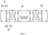
Fig. 1 is a schematic structural view of a device for bending a PCB; -
Fig. 2 is a schematic structural view of an LED module in accordance with the present invention with the device ofFig. 1 ; -
Fig. 3 is a schematic structural view of the first adjusting component and the second adjusting component of the device ofFig. 1 ; -
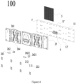
FIG. 4 is an exploded view of the LED module ofFIG. 2 . - Below, embodiments of the present invention will be described in greater detail with reference to the drawings.
- As shown in
FIG. 1 to FIG. 2 , there is provided adevice 2 for bending asheet 1 which is a PCB (printed circuit board) used in the field of electronic technology. Thesheet 1 includes a firstoutside surface 11 and a secondoutside surface 12 opposite to the firstoutside surface 11. Thedevice 2 includes at least two abutting members. Preferably, in the present embodiment, the number of the abutting members is five, the width of the three middle abutting members are the same, the width of the two abutting members located at both sides are the same, and the width of the middle abutting members is twice times the width of the abutting members located on both sides. When the PCB with LEDs mounted thereon is connected with thedevice 2, the width of each of the middle abutting members corresponds to the width of an LED display sub-area, and the width of the LED display sub-area is equal to the sum of the width of the abutting members located on both sides. The sum of the width of two abutting members located on the side of thedevice 2 equals to the width of the LED display sub-area when at least twodevices 2 are connected together, so as to form a desired arc display screen. Of course, it is also possible to provide other number of abutting members according to the actual situation, for example, the number of abutting members may be four, six or seven, etc., and such implementation manners also fall into the protection scope of the present embodiment. In addition, it is noted that, in order to clearly and briefly describe the specific structure of thedevice 2, only two of the abutting members are described in the following detailed descrciption of the embodiment. It is understood that thedevice 2 includes but is not limited to two abutting members. - Wherein the two abutting members are respectively defined as a first abutting
member 21 and a second abuttingmember 22. The first abuttingmember 21 is fixedly connected to the secondoutside surface 12 of thesheet 1. The second abuttingmember 22 is fixedly connected to the secondoutside surface 12 of thesheet 1 and is rotatably connected to the first abuttingmember 21. A rotatingposition 23 and alocking position 24 are provided at the connection of the first abuttingmember 21 and the second abuttingmember 22, the first abuttingmember 21 and the second abuttingmember 22 are capable of rotating relative to each other at the rotatingposition 23 and the first abuttingmember 21 and the second abuttingmember 22 are capable of being interlocked with each other at thelocking position 24. The first abuttingmember 21 and the second abuttingmember 22 are interlocked so as to obtain a desired curvature of thesheet 1. - The
sheet 1 is able to obtain a desired curvature by changing the rotation angle formed between the first abuttingmember 21 and the second abuttingmember 22. Thelocking position 24 is provided between the first abuttingmember 21 and the second abuttingmember 22 and therefore the maximum curvature can be limited so as to avoid damage of thesheet 1 resulted from erroneous operation. - The first abutting
member 21 comprises a firstabutting plate 211 fixedly connected to the secondoutside surface 12 of thesheet 1 and a first adjustingcomponent 212 disposed on thefirst abutting plate 211. The second abuttingmember 22 comprises a secondabutting plate 221 fixedly connected to the secondoutside surface 12 of thesheet 1 and asecond adjusting component 222 disposed on thesecond abutting plate 221. Thefirst adjusting component 212 is rotatably connected to thesecond adjusting component 222, both therotating position 23 and thelocking position 24 are formed at the connection of thefirst adjusting component 212 and thesecond adjusting component 222. The first abuttingmember 21 is mainly composed of the firstabutting plate 211 and the first adjustingcomponent 212 and the second abuttingmember 22 is mainly composed of the secondabutting plate 221 and the second adjustingcomponent 222, which accordingly, in addition to simplifying the structure, easy processing, but also is beneficial to adjust the curvature of thesheet 1. Specifically, the rotating position and the locking position are formed by the rotational connection of the first adjustingcomponent 212 and the second adjustingcomponent 222 so that the curvature of thesheet 1 is smoother. - Preferably, in order to ensure the stability of the device and the uniformity of the load-bearing of the sheet, and avoid material waste, the number of the first adjusting
component 212 and thesecond adjusting component 222 is two. Of course, the number of the first adjustingcomponent 212 and the second adjustingcomponent 222 may also be set to three, four, five, etc, and such implementation manners also fall into the protection scope of the present embodiment. - Specifically, as shown in
FIG. 3 , thefirst adjusting component 212 is provided with afirst locking protrusion 2121, thesecond adjusting component 222 is provided with afirst locking slot 2221 corresponding to the first locking protrusion2121, and thefirst adjusting component 212 is rotatably connected to thesecond adjusting component 222 by the connection of thefirst locking protrusion 2121 and thefirst locking slot 2221. A firstengaging surface 2122 is provided at an end of thefirst locking protrusion 2121 connecting with thefirst locking slot 2221, a secondengaging surface 2222 corresponding to the firstengaging surface 2122 is provided on thesecond adjusting component 222 located within thefirst locking slot 2221 locking, and the mutual rotation and locking between thefirst adjusting component 212 and thesecond adjusting component 222 are achieved by engagement of the firstengaging surface 2122 and the secondengaging surface 2222. The rotation angle formed between the first adjustingcomponent 212 and the second adjustingcomponent 222 can be conveniently adjusted so as to obtain a desired curvature of thesheet 1. Furthermore, the lock between thefirst adjusting component 212 and thesecond adjusting component 222 can be easily and conveniently unlocked, as long as thefirst adjusting component 212 and thesecond adjusting component 222 are loosened in a direction toward therotating position 23. - Moreover, the
first adjusting component 212 comprises asecond locking slot 2123, thesecond adjusting component 222 comprises asecond locking protrusion 2223 corresponding to thesecond locking slot 2123, and thefirst adjusting component 212 is rotatably connected to thesecond adjusting component 222 respectively by the locking connection of thefirst locking protrusion 2121 and thefirst locking slot 2221, as well as the locking connection of thesecond locking slot 2123 and thesecond locking protrusion 2223. A thirdengaging surface 2224 is provided at an end of thesecond locking protrusion 2223 connecting with thesecond locking slot 2123, a fourthengaging surface 2124 corresponding to the thirdengaging surface 2224 is provided on a portion of thefirst adjusting component 212 located within thesecond locking slot 2123, and the mutual rotation and locking between thefirst adjusting component 212 and thesecond adjusting component 222 are achieved respectively by engagement of the firstengaging surface 2122 and the secondengaging surface 2222, as well as engagement of the thirdengaging surface 2224 and the fourthengaging surface 2124. - Preferably, the number of the
first locking protrusion 2121, thefirst locking slot 2221, thesecond locking protrusion 2223, and thesecond locking slot 2123 can be set as more than one, for example, two, three, four, or five, etc., and such implementation manners also fall into the protection scope of the present embodiment, whereby thefirst adjusting component 212 and thesecond adjusting component 222 can be better locked. -
FIG. 4 shows an embodiment of the present invention containing the implementation content of the above. In the present embodiment, apositioning component 13 is arranged on the secondoutside surface 12 of thesheet 1, a mountinghole 25 corresponding to thepositioning component 13 is arranged on the abutting member, wherein the abutting member is the first abuttingmember 21 and / or the second abuttingmember 22. The abutting member is fixedly connected to the secondoutside surface 12 of thesheet 1 by engagement of the mountinghole 25 and thepositioning component 13. Preferably, thepositioning component 13 can be set as more than one, and the mountinghole 25 can be correspondingly set as more than one. Therefore, the abutting member could be more firmly and reliably mounted on thesheet 1 by engagement of the more than onepositioning components 13 and more than one mounting holes 25. - Preferably, the
device 2 further comprises a locking component for locking (not shown in the figure) both thesheet 1 and the abutting member, and an end of thepositioning component 13 passing through the mountinghole 25 is connected to the locking component and abuts against the abutting member. - Preferably, an end of the
positioning component 13 passing through the mountinghole 25 is provided with a threaded section, and the locking component is a screw threadably connected to the threaded section. - As shown in
FIG. 1 to FIG. 4 , thedevice 2 further comprises a connectingstructure 26 for connecting with another sheet, and the connectingstructure 26 is disposed on the abutting member. - Preferably, the connecting
structure 26 comprises: - a connecting
installation slot 261, the connectinginstallation slot 261 being disposed on the abutting member; - a connecting
component 262, the connectingcomponent 262 being rotatably disposed in the connectinginstallation slot 261, and the connectingcomponent 262 comprising a connectingportion 2621 rotatably protruding from the connectinginstallation slot 261 and a holdingportion 2622 connected to the connectingportion 2621; - a
fixing component 263, an end of thefixing component 263 being connected to the connectingcomponent 262, and the other end of thefixing component 263 being connected to the abutting member so that the connectingcomponent 262 is fixedly arranged in the connectinginstallation slot 261; - a connecting
part 264, the connectingpart 264 being disposed on the abutting member corresponding to another sheet for connection with the connectingportion 2621. - Refer to
FIG. 4 , the present invention relates to anLED module 100 in accordance with the present invention, comprising a PCB 1', LEDs, amask 3 and the above-describeddevice 2. The PCB 1' comprises a first outside surface 11' and a second outside surface 12' opposite to the first outside surface 11'; the LEDs are disposed on the first outside surface 11' of the PCB 1'; themask 3 is disposed on a first outside surface 11' of the PCB 1' and covers the LEDs; the first abuttingmember 21 and the second abuttingmember 22 are both fixedly disposed on the second outside surface 12' of the PCB 1'. - Since the
device 2 is mounted on theLED module 100, N pieces of abutting members can be used, wherein 10 ≧ N ≧ 2 and N is an integer, so that the PCB 1' is bent. The PCB 1' of the above-describedLED module 100 is fixedly connected to the abutting members, and the connection of two adjacent abutting members is close to a curved surface and the first outside surface 11' of the PCB 1' is correspondingly close to a curved surface, the point space formed between two adjacent LEDs at the connection of the abutting members is minimally changed, and the display surface of the LEDs disposed on the first outside surface 11' of the PCB 1' is closest to a curved surface so as to achieve the best curved display. Furthermore, the abutting member is fixedly connected to the secondoutside surface 12 of thesheet 1 by engagement of the mountinghole 25 and thepositioning component 13 so that the PCB 1' of theLED module 100 is easy to install and adapt to the needs of different occasions. - Moreover, the
LED module 100 further includes a data interface 4 disposed on the PCB 1' so as to facilitate the data transmission. Preferably, the number of data interface 4 is one, and the single data interface 4 is disposed at a position below the middle of the PCB 1' so as to be convenient for installation and maintenance. Meanwhile, the above single data interface 4 can also be made fool-proof so that it is not easy to be installed reversely.
Claims (8)
- An LED module (100), comprising a PCB (1'), LEDs, a mask (3) and a device (2) for bending the PCB;wherein the PCB (1') comprises a first outside surface (11) and a second outside surface (12) opposite to the first outside surface (11), the LEDs are disposed on the first outside surface (11) of the PCB (1'); the mask is disposed on the first outside surface (11) of the PCB (1') and covers the LEDs;wherein the device comprises at least two abutting members, and the two abutting members are respectively defined as a first abutting member (21) and a second abutting member (22); the first abutting member (21) is fixedly connectable to and disposed on the second outside surface (12) of the PCB (1'), the second abutting member (22) is fixedly connectable to and disposed on the second outside surface (12) of the PCB (1') and is rotatably connected to the first abutting member (21);wherein a rotating position (23) and a locking position (24) are provided at the connection of the first abutting member (21) and the second abutting member (22), the first abutting member (21) and the second abutting member (22) are capable of rotating relative to each other at the rotating position (23), and the first abutting member (21) and the second abutting member (22) are capable of being interlocked with each other at the locking position (24) so as to obtain a desired curvature of the PCB (1'); the at least two abutting members are on an inner side of the desired curvature of the PCB (1'), and the inner side of the desired curvature of the PCB (1') corresponds to the second outside surface (12) of the PCB (1');wherein the first abutting member (21) comprises a first abutting plate (211) fixedly connectable to the second outside surface (12) of the PCB (1') and a first adjusting component (212) disposed on the first abutting plate (211); the second abutting member (22) comprises a second abutting plate (221) fixedly connectable to the second outside surface (12) of the PCB (1') and a second adjusting component (222) disposed on the second abutting plate (221);wherein the first adjusting component (212) is provided with a first locking protrusion (2121) extending from a side portion of the first adjusting component (212), the second adjusting component (222) is provided with a first locking slot (2221) corresponding to the first locking protrusion (2121), the first adjusting component (212) is rotatably connected to the second adjusting component (222) by the connection between the first locking protrusion (2121) and the first locking slot (2221),wherein both the rotating position (23) and the locking position (24) are formed at the connection of the first adjusting component (212) and the second adjusting component (222), wherein both the first adjusting component (212) and the second adjusting component (222) are in the shape of "E" and the first locking protrusion (2121) is in the shape of "T".
- An LED module (100) of claim 1, characterized in that a first engaging surface (2122) is provided at an end of the first locking protrusion (2121) connecting with the first locking slot (2221), a second engaging surface (2222) corresponding to the first engaging surface (2122) is provided on a portion of the second adjusting component (222) located within the first locking slot (2221), and the mutual rotation and locking between the first adjusting component (212) and the second adjusting component (222) are achieved by engagement of the first engaging surface (2122) and the second engaging surface (2222).
- An LED module (100) of claim 2, characterized in that the first adjusting component (212) further comprises a second locking slot (2123), the second adjusting component (222) comprises a second locking protrusion (2223) corresponding to the second locking slot (2123), the second locking protrusion (2223) extends from a side portion of the second adjusting component (222); and the first adjusting component (212) is rotatably connected to the second adjusting component (222) respectively by the connection of the first locking protrusion (2121) and the first locking slot (2221) and the connection of the second locking slot (2123) and the second locking protrusion (2223); the second locking protrusion (2223) is in the shape of "T";
a third engaging surface (2224) is provided at an end of the second locking protrusion (2223) connecting with the second locking slot (2123), a fourth engaging surface corresponding to the third engaging surface (2224) is provided on a portion of the first adjusting component (212) located within the second locking slot (2123), and the mutual rotation and locking between the first adjusting component (212) and the second adjusting component (222) are achieved respectively by engagement of the first engaging surface (2122) and the second engaging surface (2222) and engagement of the third engaging surface (2224) and the fourth engaging surface. - An LED module (100) of claim 1, characterized in that a positioning component (13) is arranged on the second outside surface (12) of the PCB (1'), a mounting hole (25) for extension of the positioning component (13) is arranged on the abutting member, the abutting member is fixedly connectable to the second outside surface (12) of the PCB (1') by engagement of the mounting hole (25) and the positioning component (13).
- An LED module (100) of claim 4, characterized in that the device further comprises a locking component for locking the PCB (1') and the abutting member, and an end of the positioning component (13) passing through the mounting hole (25) is connected to the locking component and abuts against the abutting member.
- An LED module (100) of claim 5, characterized in that an end of the positioning component (13) passing through the mounting hole (25) is provided with a threaded section, and the locking component is a screw threadably connected to the threaded section.
- An LED module of claim 1, characterized in that the device further comprises a connecting structure (26) for connecting with another PCB (1'), and the connecting structure (26) is disposed on the abutting member.
- An LED module of claim 7, characterized in that the connecting structure (26) comprises:a connecting installation slot (261), the connecting installation slot (261) being disposed on the abutting member;a connecting component (262), the connecting component (262) being rotatably disposed in the connecting installation slot (261), and the connecting component (262) comprising a connecting portion (2621) rotatably protruding from the connecting installation slot (261) and a holding portion (2622) connected to the connecting portion (2621);a fixing component (263), an end of the fixing component (263) being connected to the connecting component (262), and the other end of the fixing component (263) being connected to the abutting member so that the connecting component (262) is fixedly arranged in the connecting installation slot (261);a connecting part (264), the connecting part (264) being disposed on the abutting member corresponding to another PCB (1') for connection with the connecting portion (2621).
Applications Claiming Priority (2)
| Application Number | Priority Date | Filing Date | Title |
|---|---|---|---|
| CN201720100853.1U CN206559732U (en) | 2017-01-24 | 2017-01-24 | A kind of device and LED modules for bent plate |
| PCT/CN2017/101263 WO2018137347A1 (en) | 2017-01-24 | 2017-09-11 | Device and led module for bending board |
Publications (4)
| Publication Number | Publication Date |
|---|---|
| EP3419392A1 EP3419392A1 (en) | 2018-12-26 |
| EP3419392A4 EP3419392A4 (en) | 2019-11-27 |
| EP3419392B1 true EP3419392B1 (en) | 2025-02-12 |
| EP3419392C0 EP3419392C0 (en) | 2025-02-12 |
Family
ID=60011474
Family Applications (1)
| Application Number | Title | Priority Date | Filing Date |
|---|---|---|---|
| EP17894504.4A Active EP3419392B1 (en) | 2017-01-24 | 2017-09-11 | Led module |
Country Status (4)
| Country | Link |
|---|---|
| US (1) | US10314167B2 (en) |
| EP (1) | EP3419392B1 (en) |
| CN (1) | CN206559732U (en) |
| WO (1) | WO2018137347A1 (en) |
Families Citing this family (4)
| Publication number | Priority date | Publication date | Assignee | Title |
|---|---|---|---|---|
| CN108806524B (en) * | 2018-07-06 | 2024-04-09 | 深圳市洲明科技股份有限公司 | Cabinet, display module and display device |
| CN108799266B (en) * | 2018-08-28 | 2023-12-01 | 湖南新亚胜光电股份有限公司 | Display screen connecting device and LED display screen |
| USD954147S1 (en) * | 2019-12-09 | 2022-06-07 | Roe Visual Co., Ltd. | LED display screen |
| USD954149S1 (en) * | 2020-05-20 | 2022-06-07 | H2Vr Holdco, Inc. | LED tile |
Citations (2)
| Publication number | Priority date | Publication date | Assignee | Title |
|---|---|---|---|---|
| US4930753A (en) * | 1988-08-10 | 1990-06-05 | Alvyn Alvin E | Moldable edge connecting apparatus |
| US5357728A (en) * | 1989-05-03 | 1994-10-25 | Duncanson Robert J | Jointing of building panels and sheets |
Family Cites Families (14)
| Publication number | Priority date | Publication date | Assignee | Title |
|---|---|---|---|---|
| JPH0916107A (en) * | 1995-04-28 | 1997-01-17 | Copal Co Ltd | Lightning display unit |
| JP2002047599A (en) * | 2000-07-27 | 2002-02-15 | Ono Seisakusho:Kk | Tool for plating printed circuit board |
| JP2004235228A (en) * | 2003-01-28 | 2004-08-19 | Mitsumi Electric Co Ltd | Electronic equipment |
| GB2404089B (en) * | 2003-07-11 | 2007-05-02 | Craig Rochford | Printed circuit board assembly |
| US20050057125A1 (en) * | 2003-08-08 | 2005-03-17 | Duke Manufacturing Company | Graphics display |
| CN201294678Y (en) * | 2008-10-14 | 2009-08-19 | 江苏银河电子股份有限公司 | PCB batten clip |
| FR2987833B1 (en) * | 2012-03-06 | 2014-03-14 | Saint Gobain | ARTICULATION BOMBING SUPPORT |
| US9536456B2 (en) * | 2013-07-02 | 2017-01-03 | Lg Electronics, Inc. | Image display device |
| KR20150018339A (en) * | 2013-08-08 | 2015-02-23 | 삼성전자주식회사 | Display apparatus |
| CN104797075B (en) * | 2014-01-17 | 2019-02-26 | 中兴通讯股份有限公司 | Arched PCB and its design method |
| KR102244807B1 (en) * | 2014-03-07 | 2021-04-26 | 엘지디스플레이 주식회사 | Foldable display apparatus |
| CN104465529B (en) * | 2014-07-03 | 2016-03-23 | 株洲南车时代电气股份有限公司 | Power electronics modules encapsulation shell and there is the power electronics modules of this shell |
| KR102233119B1 (en) * | 2014-09-23 | 2021-03-30 | 삼성디스플레이 주식회사 | Display device |
| CN205160921U (en) * | 2015-11-03 | 2016-04-13 | 邓育智 | PCB clamp |
-
2017
- 2017-01-24 CN CN201720100853.1U patent/CN206559732U/en active Active
- 2017-09-11 EP EP17894504.4A patent/EP3419392B1/en active Active
- 2017-09-11 WO PCT/CN2017/101263 patent/WO2018137347A1/en not_active Ceased
-
2018
- 2018-05-31 US US15/993,728 patent/US10314167B2/en active Active
Patent Citations (2)
| Publication number | Priority date | Publication date | Assignee | Title |
|---|---|---|---|---|
| US4930753A (en) * | 1988-08-10 | 1990-06-05 | Alvyn Alvin E | Moldable edge connecting apparatus |
| US5357728A (en) * | 1989-05-03 | 1994-10-25 | Duncanson Robert J | Jointing of building panels and sheets |
Also Published As
| Publication number | Publication date |
|---|---|
| US10314167B2 (en) | 2019-06-04 |
| US20180279469A1 (en) | 2018-09-27 |
| CN206559732U (en) | 2017-10-13 |
| WO2018137347A1 (en) | 2018-08-02 |
| EP3419392A4 (en) | 2019-11-27 |
| EP3419392C0 (en) | 2025-02-12 |
| EP3419392A1 (en) | 2018-12-26 |
Similar Documents
| Publication | Publication Date | Title |
|---|---|---|
| EP3249640B1 (en) | Display device | |
| EP2730968B1 (en) | Curved display apparatus | |
| US11924969B2 (en) | Display device coupled to circuit board with coupling film | |
| US9960383B2 (en) | Display device | |
| EP3315856B1 (en) | Display apparatus | |
| US9541779B2 (en) | Display device including a curvature maintaining bar | |
| CN111542778A (en) | Hinge assembly for display unit and display module | |
| US9810934B2 (en) | Display device | |
| KR20160129494A (en) | Display unit and display apparatus having the same | |
| US20100149734A1 (en) | Display apparatus | |
| US10314167B2 (en) | Device for bending sheet, LED module and display screen | |
| WO2018080051A1 (en) | Large display device having partially curved part | |
| EP1927886A2 (en) | Chassis, backlight unit, liquid crystal display having the same, and method thereof | |
| JP6927825B2 (en) | Flexible printed circuit board and display device | |
| KR101838566B1 (en) | Curved type imaging device | |
| US12495686B2 (en) | Display assembly and electronic apparatus | |
| CN108922407A (en) | Display screen and display device | |
| JP2001051619A (en) | Flat panel display | |
| KR20240066311A (en) | Manufacturing device of display device | |
| JPWO2016170621A1 (en) | LIGHT SOURCE DEVICE, DISPLAY DEVICE, SUBSTRATE UNIT MANUFACTURING METHOD, AND LIGHT SOURCE DEVICE MANUFACTURING METHOD | |
| EP4043778B1 (en) | Display device | |
| US8107249B2 (en) | Display panel apparatus | |
| JP2025111228A (en) | Display assemblies and electronic devices | |
| US20030086029A1 (en) | Fixing structure for flat display | |
| CN113823197A (en) | Display device and electronic device |
Legal Events
| Date | Code | Title | Description |
|---|---|---|---|
| STAA | Information on the status of an ep patent application or granted ep patent |
Free format text: STATUS: THE INTERNATIONAL PUBLICATION HAS BEEN MADE |
|
| PUAI | Public reference made under article 153(3) epc to a published international application that has entered the european phase |
Free format text: ORIGINAL CODE: 0009012 |
|
| STAA | Information on the status of an ep patent application or granted ep patent |
Free format text: STATUS: REQUEST FOR EXAMINATION WAS MADE |
|
| 17P | Request for examination filed |
Effective date: 20180917 |
|
| AK | Designated contracting states |
Kind code of ref document: A1 Designated state(s): AL AT BE BG CH CY CZ DE DK EE ES FI FR GB GR HR HU IE IS IT LI LT LU LV MC MK MT NL NO PL PT RO RS SE SI SK SM TR |
|
| AX | Request for extension of the european patent |
Extension state: BA ME |
|
| A4 | Supplementary search report drawn up and despatched |
Effective date: 20191024 |
|
| RIC1 | Information provided on ipc code assigned before grant |
Ipc: G09F 9/33 20060101ALI20191018BHEP Ipc: H05K 3/00 20060101AFI20191018BHEP Ipc: H05K 1/02 20060101ALN20191018BHEP |
|
| DAV | Request for validation of the european patent (deleted) | ||
| DAX | Request for extension of the european patent (deleted) | ||
| STAA | Information on the status of an ep patent application or granted ep patent |
Free format text: STATUS: EXAMINATION IS IN PROGRESS |
|
| 17Q | First examination report despatched |
Effective date: 20210914 |
|
| GRAP | Despatch of communication of intention to grant a patent |
Free format text: ORIGINAL CODE: EPIDOSNIGR1 |
|
| STAA | Information on the status of an ep patent application or granted ep patent |
Free format text: STATUS: GRANT OF PATENT IS INTENDED |
|
| RIC1 | Information provided on ipc code assigned before grant |
Ipc: H05K 1/02 20060101ALN20241113BHEP Ipc: F16B 5/00 20060101ALI20241113BHEP Ipc: G09F 9/33 20060101ALI20241113BHEP Ipc: H05K 3/00 20060101AFI20241113BHEP |
|
| GRAS | Grant fee paid |
Free format text: ORIGINAL CODE: EPIDOSNIGR3 |
|
| INTG | Intention to grant announced |
Effective date: 20241203 |
|
| GRAA | (expected) grant |
Free format text: ORIGINAL CODE: 0009210 |
|
| STAA | Information on the status of an ep patent application or granted ep patent |
Free format text: STATUS: THE PATENT HAS BEEN GRANTED |
|
| AK | Designated contracting states |
Kind code of ref document: B1 Designated state(s): AL AT BE BG CH CY CZ DE DK EE ES FI FR GB GR HR HU IE IS IT LI LT LU LV MC MK MT NL NO PL PT RO RS SE SI SK SM TR |
|
| REG | Reference to a national code |
Ref country code: GB Ref legal event code: FG4D |
|
| REG | Reference to a national code |
Ref country code: CH Ref legal event code: EP |
|
| REG | Reference to a national code |
Ref country code: DE Ref legal event code: R096 Ref document number: 602017087768 Country of ref document: DE |
|
| REG | Reference to a national code |
Ref country code: IE Ref legal event code: FG4D |
|
| U01 | Request for unitary effect filed |
Effective date: 20250227 |
|
| U07 | Unitary effect registered |
Designated state(s): AT BE BG DE DK EE FI FR IT LT LU LV MT NL PT RO SE SI Effective date: 20250307 |
|
| PG25 | Lapsed in a contracting state [announced via postgrant information from national office to epo] |
Ref country code: RS Free format text: LAPSE BECAUSE OF FAILURE TO SUBMIT A TRANSLATION OF THE DESCRIPTION OR TO PAY THE FEE WITHIN THE PRESCRIBED TIME-LIMIT Effective date: 20250512 |
|
| PG25 | Lapsed in a contracting state [announced via postgrant information from national office to epo] |
Ref country code: PL Free format text: LAPSE BECAUSE OF FAILURE TO SUBMIT A TRANSLATION OF THE DESCRIPTION OR TO PAY THE FEE WITHIN THE PRESCRIBED TIME-LIMIT Effective date: 20250212 |
|
| PG25 | Lapsed in a contracting state [announced via postgrant information from national office to epo] |
Ref country code: ES Free format text: LAPSE BECAUSE OF FAILURE TO SUBMIT A TRANSLATION OF THE DESCRIPTION OR TO PAY THE FEE WITHIN THE PRESCRIBED TIME-LIMIT Effective date: 20250212 |
|
| PG25 | Lapsed in a contracting state [announced via postgrant information from national office to epo] |
Ref country code: IS Free format text: LAPSE BECAUSE OF FAILURE TO SUBMIT A TRANSLATION OF THE DESCRIPTION OR TO PAY THE FEE WITHIN THE PRESCRIBED TIME-LIMIT Effective date: 20250612 Ref country code: NO Free format text: LAPSE BECAUSE OF FAILURE TO SUBMIT A TRANSLATION OF THE DESCRIPTION OR TO PAY THE FEE WITHIN THE PRESCRIBED TIME-LIMIT Effective date: 20250512 |
|
| PG25 | Lapsed in a contracting state [announced via postgrant information from national office to epo] |
Ref country code: HR Free format text: LAPSE BECAUSE OF FAILURE TO SUBMIT A TRANSLATION OF THE DESCRIPTION OR TO PAY THE FEE WITHIN THE PRESCRIBED TIME-LIMIT Effective date: 20250212 |
|
| PG25 | Lapsed in a contracting state [announced via postgrant information from national office to epo] |
Ref country code: GR Free format text: LAPSE BECAUSE OF FAILURE TO SUBMIT A TRANSLATION OF THE DESCRIPTION OR TO PAY THE FEE WITHIN THE PRESCRIBED TIME-LIMIT Effective date: 20250513 |
|
| U20 | Renewal fee for the european patent with unitary effect paid |
Year of fee payment: 9 Effective date: 20250826 |
|
| PG25 | Lapsed in a contracting state [announced via postgrant information from national office to epo] |
Ref country code: SM Free format text: LAPSE BECAUSE OF FAILURE TO SUBMIT A TRANSLATION OF THE DESCRIPTION OR TO PAY THE FEE WITHIN THE PRESCRIBED TIME-LIMIT Effective date: 20250212 |
|
| PGFP | Annual fee paid to national office [announced via postgrant information from national office to epo] |
Ref country code: GB Payment date: 20250919 Year of fee payment: 9 |
|
| PG25 | Lapsed in a contracting state [announced via postgrant information from national office to epo] |
Ref country code: CZ Free format text: LAPSE BECAUSE OF FAILURE TO SUBMIT A TRANSLATION OF THE DESCRIPTION OR TO PAY THE FEE WITHIN THE PRESCRIBED TIME-LIMIT Effective date: 20250212 |
|
| PG25 | Lapsed in a contracting state [announced via postgrant information from national office to epo] |
Ref country code: SK Free format text: LAPSE BECAUSE OF FAILURE TO SUBMIT A TRANSLATION OF THE DESCRIPTION OR TO PAY THE FEE WITHIN THE PRESCRIBED TIME-LIMIT Effective date: 20250212 |
|
| PLBE | No opposition filed within time limit |
Free format text: ORIGINAL CODE: 0009261 |
|
| STAA | Information on the status of an ep patent application or granted ep patent |
Free format text: STATUS: NO OPPOSITION FILED WITHIN TIME LIMIT |
|
| REG | Reference to a national code |
Ref country code: CH Ref legal event code: L10 Free format text: ST27 STATUS EVENT CODE: U-0-0-L10-L00 (AS PROVIDED BY THE NATIONAL OFFICE) Effective date: 20251224 |
|
| 26N | No opposition filed |
Effective date: 20251113 |
|
| REG | Reference to a national code |
Ref country code: CH Ref legal event code: H13 Free format text: ST27 STATUS EVENT CODE: U-0-0-H10-H13 (AS PROVIDED BY THE NATIONAL OFFICE) Effective date: 20260504 |