EP3419048A2 - Extended drain nmos transistor with buried p type region - Google Patents
Extended drain nmos transistor with buried p type region Download PDFInfo
- Publication number
- EP3419048A2 EP3419048A2 EP18166136.4A EP18166136A EP3419048A2 EP 3419048 A2 EP3419048 A2 EP 3419048A2 EP 18166136 A EP18166136 A EP 18166136A EP 3419048 A2 EP3419048 A2 EP 3419048A2
- Authority
- EP
- European Patent Office
- Prior art keywords
- region
- type
- buried
- transistor
- semiconductor layer
- Prior art date
- Legal status (The legal status is an assumption and is not a legal conclusion. Google has not performed a legal analysis and makes no representation as to the accuracy of the status listed.)
- Withdrawn
Links
Images



Classifications
-
- H—ELECTRICITY
- H10—SEMICONDUCTOR DEVICES; ELECTRIC SOLID-STATE DEVICES NOT OTHERWISE PROVIDED FOR
- H10D—INORGANIC ELECTRIC SEMICONDUCTOR DEVICES
- H10D30/00—Field-effect transistors [FET]
- H10D30/01—Manufacture or treatment
- H10D30/021—Manufacture or treatment of FETs having insulated gates [IGFET]
- H10D30/028—Manufacture or treatment of FETs having insulated gates [IGFET] of double-diffused metal oxide semiconductor [DMOS] FETs
- H10D30/0281—Manufacture or treatment of FETs having insulated gates [IGFET] of double-diffused metal oxide semiconductor [DMOS] FETs of lateral DMOS [LDMOS] FETs
-
- H—ELECTRICITY
- H10—SEMICONDUCTOR DEVICES; ELECTRIC SOLID-STATE DEVICES NOT OTHERWISE PROVIDED FOR
- H10D—INORGANIC ELECTRIC SEMICONDUCTOR DEVICES
- H10D30/00—Field-effect transistors [FET]
- H10D30/01—Manufacture or treatment
- H10D30/021—Manufacture or treatment of FETs having insulated gates [IGFET]
- H10D30/0221—Manufacture or treatment of FETs having insulated gates [IGFET] having asymmetry in the channel direction, e.g. lateral high-voltage MISFETs having drain offset region or extended-drain MOSFETs [EDMOS]
-
- H—ELECTRICITY
- H10—SEMICONDUCTOR DEVICES; ELECTRIC SOLID-STATE DEVICES NOT OTHERWISE PROVIDED FOR
- H10D—INORGANIC ELECTRIC SEMICONDUCTOR DEVICES
- H10D30/00—Field-effect transistors [FET]
- H10D30/60—Insulated-gate field-effect transistors [IGFET]
- H10D30/601—Insulated-gate field-effect transistors [IGFET] having lightly-doped drain or source extensions, e.g. LDD IGFETs or DDD IGFETs
- H10D30/603—Insulated-gate field-effect transistors [IGFET] having lightly-doped drain or source extensions, e.g. LDD IGFETs or DDD IGFETs having asymmetry in the channel direction, e.g. lateral high-voltage MISFETs having drain offset region or extended drain IGFETs [EDMOS]
-
- H—ELECTRICITY
- H10—SEMICONDUCTOR DEVICES; ELECTRIC SOLID-STATE DEVICES NOT OTHERWISE PROVIDED FOR
- H10D—INORGANIC ELECTRIC SEMICONDUCTOR DEVICES
- H10D30/00—Field-effect transistors [FET]
- H10D30/60—Insulated-gate field-effect transistors [IGFET]
- H10D30/64—Double-diffused metal-oxide semiconductor [DMOS] FETs
- H10D30/65—Lateral DMOS [LDMOS] FETs
- H10D30/657—Lateral DMOS [LDMOS] FETs having substrates comprising insulating layers, e.g. SOI-LDMOS transistors
-
- H—ELECTRICITY
- H10—SEMICONDUCTOR DEVICES; ELECTRIC SOLID-STATE DEVICES NOT OTHERWISE PROVIDED FOR
- H10D—INORGANIC ELECTRIC SEMICONDUCTOR DEVICES
- H10D62/00—Semiconductor bodies, or regions thereof, of devices having potential barriers
- H10D62/10—Shapes, relative sizes or dispositions of the regions of the semiconductor bodies; Shapes of the semiconductor bodies
- H10D62/124—Shapes, relative sizes or dispositions of the regions of semiconductor bodies or of junctions between the regions
-
- H—ELECTRICITY
- H10—SEMICONDUCTOR DEVICES; ELECTRIC SOLID-STATE DEVICES NOT OTHERWISE PROVIDED FOR
- H10D—INORGANIC ELECTRIC SEMICONDUCTOR DEVICES
- H10D62/00—Semiconductor bodies, or regions thereof, of devices having potential barriers
- H10D62/10—Shapes, relative sizes or dispositions of the regions of the semiconductor bodies; Shapes of the semiconductor bodies
- H10D62/13—Semiconductor regions connected to electrodes carrying current to be rectified, amplified or switched, e.g. source or drain regions
- H10D62/149—Source or drain regions of field-effect devices
- H10D62/151—Source or drain regions of field-effect devices of IGFETs
-
- H—ELECTRICITY
- H10—SEMICONDUCTOR DEVICES; ELECTRIC SOLID-STATE DEVICES NOT OTHERWISE PROVIDED FOR
- H10D—INORGANIC ELECTRIC SEMICONDUCTOR DEVICES
- H10D62/00—Semiconductor bodies, or regions thereof, of devices having potential barriers
- H10D62/10—Shapes, relative sizes or dispositions of the regions of the semiconductor bodies; Shapes of the semiconductor bodies
- H10D62/13—Semiconductor regions connected to electrodes carrying current to be rectified, amplified or switched, e.g. source or drain regions
- H10D62/149—Source or drain regions of field-effect devices
- H10D62/151—Source or drain regions of field-effect devices of IGFETs
- H10D62/152—Source regions of DMOS transistors
-
- H—ELECTRICITY
- H10—SEMICONDUCTOR DEVICES; ELECTRIC SOLID-STATE DEVICES NOT OTHERWISE PROVIDED FOR
- H10D—INORGANIC ELECTRIC SEMICONDUCTOR DEVICES
- H10D62/00—Semiconductor bodies, or regions thereof, of devices having potential barriers
- H10D62/10—Shapes, relative sizes or dispositions of the regions of the semiconductor bodies; Shapes of the semiconductor bodies
- H10D62/13—Semiconductor regions connected to electrodes carrying current to be rectified, amplified or switched, e.g. source or drain regions
- H10D62/149—Source or drain regions of field-effect devices
- H10D62/151—Source or drain regions of field-effect devices of IGFETs
- H10D62/156—Drain regions of DMOS transistors
- H10D62/157—Impurity concentrations or distributions
-
- H—ELECTRICITY
- H10—SEMICONDUCTOR DEVICES; ELECTRIC SOLID-STATE DEVICES NOT OTHERWISE PROVIDED FOR
- H10D—INORGANIC ELECTRIC SEMICONDUCTOR DEVICES
- H10D62/00—Semiconductor bodies, or regions thereof, of devices having potential barriers
- H10D62/10—Shapes, relative sizes or dispositions of the regions of the semiconductor bodies; Shapes of the semiconductor bodies
- H10D62/17—Semiconductor regions connected to electrodes not carrying current to be rectified, amplified or switched, e.g. channel regions
- H10D62/351—Substrate regions of field-effect devices
- H10D62/357—Substrate regions of field-effect devices of FETs
- H10D62/364—Substrate regions of field-effect devices of FETs of IGFETs
- H10D62/371—Inactive supplementary semiconductor regions, e.g. for preventing punch-through, improving capacity effect or leakage current
-
- H—ELECTRICITY
- H10—SEMICONDUCTOR DEVICES; ELECTRIC SOLID-STATE DEVICES NOT OTHERWISE PROVIDED FOR
- H10D—INORGANIC ELECTRIC SEMICONDUCTOR DEVICES
- H10D62/00—Semiconductor bodies, or regions thereof, of devices having potential barriers
- H10D62/10—Shapes, relative sizes or dispositions of the regions of the semiconductor bodies; Shapes of the semiconductor bodies
- H10D62/17—Semiconductor regions connected to electrodes not carrying current to be rectified, amplified or switched, e.g. channel regions
- H10D62/393—Body regions of DMOS transistors or IGBTs
-
- H—ELECTRICITY
- H10—SEMICONDUCTOR DEVICES; ELECTRIC SOLID-STATE DEVICES NOT OTHERWISE PROVIDED FOR
- H10D—INORGANIC ELECTRIC SEMICONDUCTOR DEVICES
- H10D86/00—Integrated devices formed in or on insulating or conducting substrates, e.g. formed in silicon-on-insulator [SOI] substrates or on stainless steel or glass substrates
- H10D86/01—Manufacture or treatment
-
- H—ELECTRICITY
- H10—SEMICONDUCTOR DEVICES; ELECTRIC SOLID-STATE DEVICES NOT OTHERWISE PROVIDED FOR
- H10D—INORGANIC ELECTRIC SEMICONDUCTOR DEVICES
- H10D86/00—Integrated devices formed in or on insulating or conducting substrates, e.g. formed in silicon-on-insulator [SOI] substrates or on stainless steel or glass substrates
- H10D86/201—Integrated devices formed in or on insulating or conducting substrates, e.g. formed in silicon-on-insulator [SOI] substrates or on stainless steel or glass substrates the substrates comprising an insulating layer on a semiconductor body, e.g. SOI
-
- H—ELECTRICITY
- H10—SEMICONDUCTOR DEVICES; ELECTRIC SOLID-STATE DEVICES NOT OTHERWISE PROVIDED FOR
- H10D—INORGANIC ELECTRIC SEMICONDUCTOR DEVICES
- H10D62/00—Semiconductor bodies, or regions thereof, of devices having potential barriers
- H10D62/10—Shapes, relative sizes or dispositions of the regions of the semiconductor bodies; Shapes of the semiconductor bodies
- H10D62/102—Constructional design considerations for preventing surface leakage or controlling electric field concentration
- H10D62/103—Constructional design considerations for preventing surface leakage or controlling electric field concentration for increasing or controlling the breakdown voltage of reverse-biased devices
- H10D62/105—Constructional design considerations for preventing surface leakage or controlling electric field concentration for increasing or controlling the breakdown voltage of reverse-biased devices by having particular doping profiles, shapes or arrangements of PN junctions; by having supplementary regions, e.g. junction termination extension [JTE]
- H10D62/106—Constructional design considerations for preventing surface leakage or controlling electric field concentration for increasing or controlling the breakdown voltage of reverse-biased devices by having particular doping profiles, shapes or arrangements of PN junctions; by having supplementary regions, e.g. junction termination extension [JTE] having supplementary regions doped oppositely to or in rectifying contact with regions of the semiconductor bodies, e.g. guard rings with PN or Schottky junctions
-
- H—ELECTRICITY
- H10—SEMICONDUCTOR DEVICES; ELECTRIC SOLID-STATE DEVICES NOT OTHERWISE PROVIDED FOR
- H10D—INORGANIC ELECTRIC SEMICONDUCTOR DEVICES
- H10D64/00—Electrodes of devices having potential barriers
- H10D64/20—Electrodes characterised by their shapes, relative sizes or dispositions
- H10D64/27—Electrodes not carrying the current to be rectified, amplified, oscillated or switched, e.g. gates
- H10D64/311—Gate electrodes for field-effect devices
- H10D64/411—Gate electrodes for field-effect devices for FETs
- H10D64/511—Gate electrodes for field-effect devices for FETs for IGFETs
- H10D64/514—Gate electrodes for field-effect devices for FETs for IGFETs characterised by the insulating layers
- H10D64/516—Gate electrodes for field-effect devices for FETs for IGFETs characterised by the insulating layers the thicknesses being non-uniform
Definitions
- This invention relates in general to transistors and more specifically to an N type extended drain transistor with a buried P type region.
- An extended drain transistor such as a laterally diffused MOSFET (LDMOS) generally includes a drain region that is electrically spaced apart from a channel region by a drift region. When in a conductive state, the charge carriers flow from the source, through the channel region, through the drift region, to the drain region.
- Extended drain transistors are typically used in high frequency and/or high voltage applications such as for high power RF amplifiers, power switches, and power supplies.
- an N type extended drain transistor can be implemented in an P type epi body region formed over a buried dielectric layer.
- an N type extended drain transistor formed from a semiconductor on insulator (SOI) wafer.
- the transistor has a buried P type region formed by the implantation of P type dopants in a semiconductor layer of the wafer at a location directly below a drift region of the transistor.
- the transistor also includes a source located in a P well region and a drain.
- the buried P type region is in electrical contact with the P well region.
- the N type drift region, the source, and the drain are also located in a portion of the semiconductor layer that is laterally surrounded by dielectric isolation.
- the semiconductor layer has a thickness of 2 microns or less.
- the buried P type region has a net conductivity of P type dopants at a sufficient concentration to ensure full drift region depletion under reverse drain bias when the substrate is biased at a higher voltage than the source of the transistor.
- the buried P type region has a sufficient doping to provide an additional mechanism for depleting the N type drift region from the bottom counteracting the higher substrate bias voltage.
- providing a buried P type region of sufficient doping allows for a fully depleted drift region under such conditions where the transistor body thickness (the thickness of the semiconductor layer) is relatively thin (e.g. as compared to the thickness of the buried dielectric layer) when the substrate voltage is higher than the source voltage.
- the semiconductor layer has a first thickness and is located above a buried dielectric layer of the SOI wafer that has a second thickness. The first thickness being in a range from 5 times greater or less than the second thickness.
- FIG 1 is a partial cross sectional side view of a wafer 101 during a stage in a manufacture of an N type extended drain transistor according to one embodiment of the present invention.
- Wafer 101 includes a substrate 103 of a mono crystalline semiconductor material (e.g. silicon) which has specific crystal orientation (e.g. ⁇ 100>). In Figure 1 , only a top portion of substrate 103 is shown.
- a buried dielectric layer 105 e.g. oxide
- a semiconductor layer 107 is located over layer 105.
- layer 107 is a monocrystalline semiconductor material (e.g. silicon) that is formed by a smart cut process (e.g. transferred monocrystalline silicon from another wafer.
- layer 107 may be formed by a different process (e.g. epitaxially grown). In one embodiment, at this stage, layer 107 has net P type doping concentration of 1 X 10 15 cm -3 . However, layer 107 may be made of different materials and/or have different doping profiles in other embodiments.
- layer 105 has a thickness in the range of 0.3 - 3 microns and layer 107 has a thickness in the range of 0.1 - 2 microns. In one specific example, layer 105 is 1.0 microns thick and layer 107 is 1.4 microns thick. In some embodiments, layer 107 has a thickness in the range of 5 times greater or less the thickness of layer 105. However, in other embodiments, layers 105 and 107 maybe of other thicknesses. In other embodiments, layer 107 can be made of multiple layers of semiconductor material.
- an N- type dopant e.g. phosphorous
- the N type dopant is implanted at a dose in the range of 1x10 12 to 1 x 10 13 cm -2 and at an energy in the range of 90 to 130 KeV. After implantation, the wafer is annealed to activate the dopants.
- Isolation structures 109, 111, 113, and 115 are formed at the upper portion of layer 107.
- structures 109, 111, 113, and 115 are made of oxide and are formed by a LOCOS process.
- these isolation structures may be formed by other processes and/or be made of other dielectric materials.
- the isolation structures can be formed by forming trenches in layer 107 and filling the trenches with a dielectric material.
- dielectric structures 109, 111, 113, and 115 are separate structures. However, in other embodiments, these structures may be physically joined at one or more locations.
- structures 111 and 113 may be part of a "doughnut shaped" isolation structure.
- P well regions 117 and 118 are formed by one or more implants of P type dopants.
- a second higher concentration of P type dopants forms the deep implanted regions 121 and 122 of P well regions 117 and 118, respectively.
- these additional implants at a higher dose and a lower energy are added for improved robustness.
- P well regions 117 and 118 may be formed by other processes, include a different number of implantation steps, and/or be implanted at different energies and/or different doses.
- N well region 119 is formed by the selective implantation of an N type dopant (e.g. phosphorous, arsenic) at a dose in the range of 1x10 12 to 1x10 13 cm -2 and an energy in a range of 400 to 500 KeV through a patterned mask (not shown) formed on wafer 101.
- N well region 119 may be formed at other doses and/or other energies.
- the ions forming P well regions 117 and 118 are implanted deeper than the ions forming N well region 119.
- the implantation steps for forming the regions of Figure 1 can be performed in any order.
- FIG. 2 is a partial cross sectional side view of wafer 101 at a subsequent stage during its manufacture.
- N type drift regions 201, 203, and 205 are formed by the selective implantation of N type ion dopants into layer 107.
- N type ions e.g. phosphorous, arsenic
- separate N type drift regions 201 and 205 are formed from N type drift region 203 to minimize the transistor on-state resistance.
- regions 201 and 205 are not present.
- region 203 has an oval doughnut shape that surrounds N well region 119.
- each side of region 203 in Figure 2 may be physically separate regions.
- drift regions 201, 203, and 205 after the formation of drift regions 201, 203, and 205, a shallow implant of P type dopant ions (not shown) is made to adjust the voltage threshold of subsequently formed transistors on wafer 101.
- Figure 3 shows a partial cutaway side view after P type dopant ions (e.g. boron) are implanted to form buried P type region 301.
- the P type ions are implanted at an energy in the range 550 to 650keV and at a dose in the range of 1 X 10 12 to 1 X 10 13 cm -2 , but may be implanted at other energies and/or other dosages in other embodiments.
- the implant energy may depend on the thickness of layer 107.
- the dopants are activated by an anneal of wafer 101.
- region 301 extends from the top surface of buried dielectric layer 105 to the bottom of P well regions 117 and 118 to where region 301 is in electrical contact with regions 117 and 118. Because N well region 119 and drift region 203 are not as deep as regions 117 and 118, buried P type region 301 does not contact N well region 119 or drift region 203 in the embodiment shown.
- region 301 has a thickness in the range of .1 to .5 microns (e.g..4 microns) but may have other thicknesses in other embodiments. In one embodiment, the thickness of region 301 is in the range of .1 to .3 of the thickness of layer 107, but may be of other ratios in other embodiments.
- FIG. 4 is a partial cutaway side view of wafer 101 after gates 403 and 407 are formed.
- gates 403 and 407 are formed by forming a layer of polysilicon or other gate material over wafer 101 and then patterning the layer of polysilicon with a photolithographic process.
- layer 107 Prior to forming the layer of gate material, layer 107 is oxidized to form a layer of oxide that is patterned with the layer of gate material to form gate dielectrics 401 and 405.
- the dielectrics 401 and 405 have a thickness in the range of 5 to 10 nm, but may have other thicknesses in other embodiments.
- the gate dielectric layer may be formed from a deposition process where the layer of gate dielectric material is deposited on wafer 101.
- side wall spacers 409 and 411 are formed on the side walls of gates 407 and 407, respectively.
- sidewall spacers 409 and 411 are made of nitride and are formed from the anisotropic etching of a layer of nitride formed on wafer 101.
- Source regions 415 and 419 and drain region 417 are formed by the implantation of N type dopant ions in wafer 101, followed by an anneal of wafer 101.
- regions 415, 419, and 417 are formed by the selective implant of N type dopant ions into wafer 101 at a dose in the range of 5 x 10 14 to 5x 10 15 cm -2 and at an energy in the range 20 - 60 KeV, but may be formed of other doses and at other energies in other embodiments.
- P type dopant ions e.g. Boron
- a patterned mask not shown
- Silicide structures are formed on wafer 101 to be in electrical contact with both the adjacent source and body contact regions to bias the body contact and source regions at the same potential during operation.
- the body contact regions 413 and 421 may be located separately from the source regions 415 and 419 and may be biased at a different voltage than the source regions.
- Transistor 425 includes gate 403, source region 415, body contact region 413, drain region 417, and drift regions 201 and 203.
- Transistor 427 includes gate 407, source region 419, body contact region 421, drain region 417, and drift regions 205 and 203.
- Buried P type region 301 serves as a reduced surface field (RESURF) region for both transistors.
- RSURF reduced surface field
- only one transistor would be shown in Figure 4 where gates 403 and 407, body contact regions 413 and 421, source regions 415 and 419, and P well regions 117 and 118 are physically connected to their respective structures and regions on each side of N well 119.
- silicide structures are formed on the source regions, drain regions, body contract regions, and gates for electrically coupling of those regions and structures.
- Interconnect structures are formed over wafer 101 for electrically interconnecting the silicide structures to other devices formed on wafer 101 to external connectors such as bond pads (not shown) that are formed on wafer 101.
- conductive field plates maybe be located above the top surface of wafer 101 (at the stage shown in Figure 4 ) in the interconnect layers with at least portions located directly above the drift regions 201, 203, and 205.
- the field plates act to provide a RESURF effect by depleting the N type drift regions form the top during operation.
- these field plates may be electrically tied to the source regions 415 and 419.
- wafer 101 is singulated into multiple die with each die including transistors similar to those shown in Figure 4 .
- the die are packaged in semiconductor packages (e.g. leaded, leadless, BGA, QFN, QFP, or wafer level packaging).
- semiconductor packages e.g. leaded, leadless, BGA, QFN, QFP, or wafer level packaging.
- the manufacture of a die as described above may include a number of other processes such as cleaning processes.
- Figure 5 shows a partial top view of wafer 101 with three active areas 503, 505 and 507.
- a plurality of P type extended drain transistors (represented by symbol 511) are formed in area 503.
- Extended drain N type transistors (including transistors 425 and 427) are formed in area 505.
- Area 507 includes a number of CMOS transistors (represented by symbol 515).
- An isolation structure 501 laterally surrounds each active area 503, 505, and 507 and includes openings for the active areas.
- the isolation structure 501 extends at least from the top surface of layer 107 to the buried dielectric layer 105.
- structure 501 is made of oxide and is formed by removing portions of layer 107 at selective locations and filling partly or entirely with oxide.
- Structure 501 can be made by other processes (e.g. LOCOS) in other embodiments.
- each area is laterally surrounded by a single contiguous isolation structure (501) to provide dielectric isolation.
- an active area may be laterally surrounded by dielectric isolation with multiple dielectric structures.
- buried P type region 301 does not extend to the inner side of dielectric structure 501.
- a lateral gap 509 exists between the inner side of structure 501 and the outer extent of region 301.
- this lateral gap is at least .1 micron (e.g..3 microns) after activation, but may be of other values in other embodiments depending on manufacturing tolerances.
- leaving a lateral gap between the edge of region 301 and the inner side of structure 501 surrounding area 505 may provide a process that does not implant or otherwise drive P type dopants into the isolation structure 501 to undesirably charge the isolation structure during operation.
- region 301 extends to the inner side of dielectric structure 501.
- the P type dopants that form region 301 are not implanted into areas 503 and 507. Utilizing an implantation process to implant the P type ions to form region 301 allows for the ability to selectively apply such a relatively heavy doping of P type ions in area 505, without affecting the other areas (503, 507) of wafer 101. If the P type doping concentration for region 301 was epitaxially grown or blanket implanted in layer 107, then the other N type regions (203, 119, 415, 419) of layer 107 would require a much heavier counter doping.
- region 301 extends all the way directly under N drift regions 203 and N well region 119. However, in other embodiments, region 301 would not extend to directly under N well region 119. Also in some embodiments, region 301 would only partially extend under N drift region 203.
- Figure 6 is a circuit diagram of circuit 601 that utilizes transistors 611 and 425 to provide a positive or negative voltage to a load 613.
- Circuit 601 is a symmetrical power supply that is capable of providing power to LOAD 613 at a voltage (VOUT) as high as VDD or as low as VSS (-VDD in the embodiment shown) during operation.
- circuit 601 includes an AC source 603, resistors 605 and 609, an amplifier 607, extended drain transistor 611, and extended drain transistor 425.
- Amplifier 607 provides a differential output.
- AC source 603 provides an AC voltage to the non-inverting input of amplifier 607.
- the inverting input of amplifier 607 receives a feedback signal based on VOUT that is reduced by the voltage divider formed by resistors 605 and 609. Based on the voltage of AC source 603 and the voltage of VOUT, amplifier 607 provides a control signal to the gate of transistor 611 and a complementary control signal to the gate of transistor 425.
- the source of transistor 611 and the drain of transistor 425 are coupled together to provide a VOUT that ranges between VDD and VSS (-VDD in the embodiment shown) based on the voltage of the output of amplifier 607.
- the feedback signal causes VOUT to track the voltage of AC source 603.
- the voltage of the complementary output of amplifier 607 can range from VSS to VDD. Accordingly, the gate voltage on transistor 425 can have the same voltage range.
- the voltage (V B ) of the body of transistor 425 is biased at the voltage (Vs) of the source region 415, which in the embodiment shown is -VDD.
- substrate 103 of the die of transistor 425 is tied to ground. Accordingly, the source voltage is biased at a voltage below the substrate during operation.
- VSS can be set at a voltage below ground (e.g. 0 to -200V) depending on the design of the circuit.
- the voltage of substrate 103 can be biased to a voltage above ground and Vs can be at ground.
- the VSS voltage is continuously applied to the source region of transistor 425 and a ground voltage is continuously applied to substrate 103 during operation. In other embodiments, different voltages can be applied to either the source or substrate at different times during the operation of the circuit.
- circuit 601 provides an alternating voltage between VDD and VSS to an external load 613 which can be e.g. an output filter of an amplifier for a speaker or antennae.
- an external load 613 can be e.g. an output filter of an amplifier for a speaker or antennae.
- circuit 601 can be used in other applications (e.g. communication system, industrial control systems, automobiles, RF applications).
- extended drain transistors 611 and 425 allows for VOUT to have a wide voltage swing (e.g. 400 volts) and/or to have a high current capacity.
- transistor 611 is located in another area (e.g.
- the devices may be implemented on separate die.
- transistor 425 can be implemented in other types of circuits (e.g. in a power amplifier circuit for a communication system).
- transistor 427 may be implemented with transistor 425 in parallel.
- an extended drain transistor (425) implemented on an SOI substrate may advantageously provide for a semiconductor device capable of high side operation (source voltage above substrate voltage) and low side operation (source voltage below substrate voltage) with latch-up immunity. Such properties may in useful in failsafe circuits such as in automotive applications and/or inductively loaded drivers.
- forming a transistor in a semiconductor layer that is 2 microns or less may enable the formation of a transistor without the utilization of deep isolation trenches to achieve isolation of the transistor active areas (e.g. 503, 505, 507). Accordingly, a high voltage transistor capable of low side operation may be formed in a cost-efficient manner. Furthermore, in some embodiments, having a semiconductor layer 107 of 2 microns or less may allow for the formation of a transistor on a wafer without having to further epitaxially grow semiconductor material on a semiconductor layer 107, thereby reducing processing costs and complexities.
- Utilizing a semiconductor layer (107) that is relatively thin with respect to the thickness of a buried dielectric layer (105) (e.g. where the ratio of the thickness of layer 107 to the thickness of layer 105 is 5 times or less) may provide for a high voltage transistor with desirable Ron*A characteristics where a double RESURF effect is utilized.
- Ron is the on-resistance in conductive state and A is the active transistor surface area.
- a double RESURF effect is utilized to deplete the N type drift regions (e.g. 201, 203, 205, and a portion of layer 107 between region 301 and drift region 203 which acts as a drift region) from the top by a conductive field plate (located above wafer 101 in the view of Figure 4 but not shown in Figure 4 ) or from the top by an elongated gate structure (403 and 407) as well as from the bottom by the capacitance from a biased substrate (103)/buried dielectric layer (105) of an SOI substrate.
- the bottom RESURF effect from the bottom capacitance of the substrate/buried dielectric layer capacitance may be absent when the substrate (103) is biased at a voltage above the source region (415).
- the off-state breakdown voltage (BVdsOFF) decreases as the source voltage drops below the substrate voltage. This is especially problematic where the semiconductor layer (107), in which the transistor is formed, is relatively thin (e.g. 5 times or less the thickness of) as compared to the thickness of the buried dielectric layer (105).
- the p-n junction formed between the relatively heavily doped (e.g. dose in the range of 1 x 10 12 to 1 x 10 13 cm -2 or higher in some embodiments) buried P type region (301) and the N type drift regions (201, 203, and 205 and a portion of layer 107) provides an additional bottom side RESURF mechanism for depleting the N type drift regions (201, 203, 205, and a portion of layer 107) from the bottom when the substrate voltage is above the source voltage (VS). Because region 301 is electrically connected to the P well region (117), region 301 is biased at the same voltage as the source region 415 during operation so as the provide the bottom RESURF mechanism even if the source voltage is below the substrate voltage.
- providing a relatively heavily doped buried P type region (301) may enable the N type drift regions 201, 203, 205, and a portion of layer 107 to be more heavily doped, which lowers drift region resistance and improves the Ron *A characteristics of the transistor.
- adding a relatively heavily doped buried P type region may improve the BVdsOFF over a transistor without such a region by over 30% at source voltages greater than 50 Volts below the substrate voltage.
- the buried P type region 301 is sufficiently doped (e.g.
- the N type drift regions 201, 203, 205, and a portion of layer 107 is fully depleted before the voltage gradients become high enough for junction breakdown to occur.
- one object when one object is "directly above” another object, it includes a portion that is above a portion of the another object in a line that is perpendicular and extends outward from a major active side of a substrate.
- body contact region 413 is directly above region 121 but is not directly above N type drift region 203.
- Gate 403 is directly above N type drift region 201 but is not directly above region 413.
- N type drift region 201 is directly below gate 403 but is not directly below gate 407.
- a method of making a transistor includes forming a source region and a drain region of a transistor in a semiconductor layer of a wafer.
- the semiconductor layer is located over a buried dielectric layer of the wafer, and the buried dielectric layer is located over a semiconductor substrate of the wafer.
- the semiconductor layer has a first thickness of 2 microns or less.
- the source region and the drain region each have an N type net doping profile.
- the source region is formed in a P type well region of the semiconductor layer.
- the method includes forming an N type drift region of the transistor with an N type net doping profile in the semiconductor layer. During a conductive state of the transistor, a current path is formed between the drain region and the source region through the N type drift region.
- the method includes forming a dielectric isolation structure.
- the N type drift region including a portion located directly below the dielectric isolation structure.
- the method includes forming a gate structure of the transistor over the semiconductor layer and selectively implanting P type dopant ions into the wafer to form a buried P type region in the semiconductor layer.
- the buried P type region has a P type net doping profile.
- the buried P type region is located directly below at least a portion of the N type drift region of the transistor.
- the buried P type region is in electrical contact with the P type well region.
- the drain region, the source region, and the N type drift region are located in a first area of the wafer wherein the semiconductor layer of the first area is laterally surrounded by dielectric isolation.
- the buried dielectric layer electrically isolates the semiconductor layer of the first area from the semiconductor substrate.
- the buried P type region contacts an upper surface of the buried dielectric layer.
- the selectively implanting includes implanting P type dopant ions at a dose in a range of 1 x 10¹² to 1 x 1013 cm-2.
- the buried dielectric layer extends to a second area of the wafer.
- the second area includes a P type transistor.
- the selectively implanting does not include implanting P type dopant ions in the second area.
- the buried dielectric layer extends to a second area of the wafer.
- the second area includes an N type transistor.
- the selectively implanting does not include implanting P type dopant ions in the second area. 6
- the dielectric isolation includes an inner side surrounding the area of the wafer.
- the buried P type region is laterally separated from the inner side by at least a first distance.
- the first distance is .1 micron or greater.
- the semiconductor layer includes an N type well, the drain region located in the N type well, a first portion of the N type drift region is located on a first side of the N type well and a second portion of the N type drift region is located on an opposite side of the N type well.
- the buried P type region is directly below the first portion, the N type well, and the second portion.
- the buried P type region is not in electrical contact with the first portion, the N type well, and the second portion.
- the semiconductor layer includes a second P type well with a second source region located in the second P type well region.
- the method further comprises singulating the wafer into a plurality of integrated circuit dies.
- a die of the plurality of integrated circuit dies includes the transistor.
- the buried P type region is directly below at least a portion of the drain region.
- Another embodiment includes a method for operating an extended drain transistor implemented in a die.
- the die includes a semiconductor layer, a semiconductor substrate, and a buried dielectric layer located between the semiconductor layer and the semiconductor substrate.
- the semiconductor layer has a first thickness that is 2 microns or less.
- the semiconductor layer includes a portion located in a first area of the die and is laterally surrounded by dielectric isolation.
- the portion of the semiconductor layer located in the first area includes a source region, a drain region, an N type drift region, and a buried P type region.
- the buried dielectric layer electrically isolates the portion of the semiconductor layer located in the first area from the semiconductor substrate.
- the method includes applying a first voltage to the semiconductor substrate and applying a second voltage to the source region concurrently with the applying the first voltage.
- the first voltage is greater than the second voltage.
- the buried P type region is located directly below the N type drift region and directly above the buried dielectric layer.
- the source region is located in a P type well in the portion of the semiconductor layer, the buried P type region is in electrical contact with the P type well region.
- the first voltage in a range of 10 to 200 volts greater than the second voltage.
- the N type drift region is fully depleted when the first voltage is at a voltage in a range of 10 to 200 volts greater than the second voltage.
- the extended drain transistor is implemented in a power supply circuit. The method further comprising providing a negative voltage at an output of the power supply circuit coupled to the drain region.
- the power supply circuit includes a second extended drain transistor in series with the extended drain transistor. The second extended drain transistor is implemented in a second area of the die with the dielectric isolation located laterally between the first area and the second area.
- the buried dielectric layer has a second thickness, the first thickness being in a range from 5 times greater or less than the second thickness.
Landscapes
- Element Separation (AREA)
- Metal-Oxide And Bipolar Metal-Oxide Semiconductor Integrated Circuits (AREA)
- Insulated Gate Type Field-Effect Transistor (AREA)
- Thin Film Transistor (AREA)
Abstract
Description
- This invention relates in general to transistors and more specifically to an N type extended drain transistor with a buried P type region.
- An extended drain transistor, such as a laterally diffused MOSFET (LDMOS), generally includes a drain region that is electrically spaced apart from a channel region by a drift region. When in a conductive state, the charge carriers flow from the source, through the channel region, through the drift region, to the drain region. Extended drain transistors are typically used in high frequency and/or high voltage applications such as for high power RF amplifiers, power switches, and power supplies. In some embodiments, an N type extended drain transistor can be implemented in an P type epi body region formed over a buried dielectric layer.
- The present invention may be better understood, and its numerous objects, features, and advantages made apparent to those skilled in the art by referencing the accompanying drawings.
-
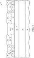
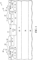
Figures 1-4 are partial cutaway side views of a wafer during various stages in the manufacture of a transistor according to one embodiment of the present invention. -
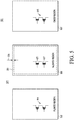
Figure 5 is a partial top view of a wafer during the manufacture of a transistor according to one embodiment of the present invention. -
Figure 6 is a circuit diagram of a circuit implementing a transistor according to one embodiment of the present invention. - The use of the same reference symbols in different drawings indicates identical items unless otherwise noted. The Figures are not necessarily drawn to scale.
- The following sets forth a detailed description of a mode for carrying out the invention. The description is intended to be illustrative of the invention and should not be taken to be limiting.
- Described herein is an N type extended drain transistor formed from a semiconductor on insulator (SOI) wafer. The transistor has a buried P type region formed by the implantation of P type dopants in a semiconductor layer of the wafer at a location directly below a drift region of the transistor. The transistor also includes a source located in a P well region and a drain. The buried P type region is in electrical contact with the P well region. The N type drift region, the source, and the drain are also located in a portion of the semiconductor layer that is laterally surrounded by dielectric isolation. The semiconductor layer has a thickness of 2 microns or less.
- In one embodiment, the buried P type region has a net conductivity of P type dopants at a sufficient concentration to ensure full drift region depletion under reverse drain bias when the substrate is biased at a higher voltage than the source of the transistor. The buried P type region has a sufficient doping to provide an additional mechanism for depleting the N type drift region from the bottom counteracting the higher substrate bias voltage. In some embodiments, providing a buried P type region of sufficient doping allows for a fully depleted drift region under such conditions where the transistor body thickness (the thickness of the semiconductor layer) is relatively thin (e.g. as compared to the thickness of the buried dielectric layer) when the substrate voltage is higher than the source voltage. In one embodiment, the semiconductor layer has a first thickness and is located above a buried dielectric layer of the SOI wafer that has a second thickness. The first thickness being in a range from 5 times greater or less than the second thickness.
-
Figure 1 is a partial cross sectional side view of awafer 101 during a stage in a manufacture of an N type extended drain transistor according to one embodiment of the present invention. Wafer 101 includes asubstrate 103 of a mono crystalline semiconductor material (e.g. silicon) which has specific crystal orientation (e.g. <100>). InFigure 1 , only a top portion ofsubstrate 103 is shown. A buried dielectric layer 105 (e.g. oxide) is located onsubstrate 103. Asemiconductor layer 107 is located overlayer 105. In one embodiment,layer 107 is a monocrystalline semiconductor material (e.g. silicon) that is formed by a smart cut process (e.g. transferred monocrystalline silicon from another wafer. However, in other embodiments,layer 107 may be formed by a different process (e.g. epitaxially grown). In one embodiment, at this stage,layer 107 has net P type doping concentration of 1 X 1015 cm-3. However,layer 107 may be made of different materials and/or have different doping profiles in other embodiments. - In some embodiments,
layer 105 has a thickness in the range of 0.3 - 3 microns andlayer 107 has a thickness in the range of 0.1 - 2 microns. In one specific example,layer 105 is 1.0 microns thick andlayer 107 is 1.4 microns thick. In some embodiments,layer 107 has a thickness in the range of 5 times greater or less the thickness oflayer 105. However, in other embodiments,layers layer 107 can be made of multiple layers of semiconductor material. - In some embodiments where
layer 107 has a net P type doping concentration, an N- type dopant (e.g. phosphorous) is implanted inlayer 107 to give layer 107 a net N type doping profile. In one embodiment, the N type dopant is implanted at a dose in the range of 1x10¹² to 1 x 1013 cm-2 and at an energy in the range of 90 to 130 KeV. After implantation, the wafer is annealed to activate the dopants. -
Isolation structures layer 107. In one embodiment,structures layer 107 and filling the trenches with a dielectric material. In the embodiment shown,dielectric structures structures -
P well regions P well regions wafer 101. A second higher concentration of P type dopants forms the deep implantedregions P well regions regions - N
well region 119 is formed by the selective implantation of an N type dopant (e.g. phosphorous, arsenic) at a dose in the range of 1x10¹² to 1x1013 cm-2 and an energy in a range of 400 to 500 KeV through a patterned mask (not shown) formed onwafer 101. However, in other embodiments, Nwell region 119 may be formed at other doses and/or other energies. In one embodiment, the ions formingP well regions well region 119. The implantation steps for forming the regions ofFigure 1 can be performed in any order. -
Figure 2 is a partial cross sectional side view ofwafer 101 at a subsequent stage during its manufacture. Ntype drift regions layer 107. In one embodiment, N type ions (e.g. phosphorous, arsenic) are implanted intolayer 107 at an energy in the range of 200 to 250keV and a dose in the range of 5 x 10¹¹ to 5 x 1012 cm-2, but may be implanted at other energies and/or other dosages in other embodiments. In the embodiment shown, separate Ntype drift regions type drift region 203 to minimize the transistor on-state resistance. However, in other embodiments,regions region 203 has an oval doughnut shape that surroundsN well region 119. However, in other embodiments, each side ofregion 203 inFigure 2 may be physically separate regions. - In some embodiments, after the formation of
drift regions wafer 101. -
Figure 3 shows a partial cutaway side view after P type dopant ions (e.g. boron) are implanted to form buriedP type region 301. In one embodiment, the P type ions are implanted at an energy in the range 550 to 650keV and at a dose in the range of 1 X 10¹² to 1 X 1013 cm-2, but may be implanted at other energies and/or other dosages in other embodiments. In some embodiments, the implant energy may depend on the thickness oflayer 107. After implantation, the dopants are activated by an anneal ofwafer 101. - In the embodiment shown,
region 301 extends from the top surface of burieddielectric layer 105 to the bottom of P wellregions region 301 is in electrical contact withregions N well region 119 and driftregion 203 are not as deep asregions P type region 301 does not contactN well region 119 or driftregion 203 in the embodiment shown. In one embodiment,region 301 has a thickness in the range of .1 to .5 microns (e.g..4 microns) but may have other thicknesses in other embodiments. In one embodiment, the thickness ofregion 301 is in the range of .1 to .3 of the thickness oflayer 107, but may be of other ratios in other embodiments. -
Figure 4 is a partial cutaway side view ofwafer 101 aftergates gates wafer 101 and then patterning the layer of polysilicon with a photolithographic process. Prior to forming the layer of gate material,layer 107 is oxidized to form a layer of oxide that is patterned with the layer of gate material to formgate dielectrics dielectrics wafer 101. - After the formation of
gates side wall spacers gates sidewall spacers wafer 101. - After the formation of
spacers source regions region 417 are formed by the implantation of N type dopant ions inwafer 101, followed by an anneal ofwafer 101. In one embodiment,regions wafer 101 at a dose in the range of 5 x 10¹⁴ to 5x 1015 cm-2 and at an energy in the range 20 - 60 KeV, but may be formed of other doses and at other energies in other embodiments. - In the embodiment shown, P type dopant ions (e.g. Boron) are selectively implanted through a patterned mask (not shown) to form
body contact regions regions wafer 101 to be in electrical contact with both the adjacent source and body contact regions to bias the body contact and source regions at the same potential during operation. However, in other embodiments, thebody contact regions source regions - Two
transistors Figure 4 .Transistor 425 includesgate 403,source region 415,body contact region 413,drain region 417, and driftregions Transistor 427 includesgate 407,source region 419,body contact region 421,drain region 417, and driftregions P type region 301 serves as a reduced surface field (RESURF) region for both transistors. In other embodiment, only one transistor would be shown inFigure 4 wheregates body contact regions source regions regions - After the stage of
Figure 4 , silicide structures are formed on the source regions, drain regions, body contract regions, and gates for electrically coupling of those regions and structures. Interconnect structures are formed overwafer 101 for electrically interconnecting the silicide structures to other devices formed onwafer 101 to external connectors such as bond pads (not shown) that are formed onwafer 101. In some embodiments, conductive field plates (not shown) maybe be located above the top surface of wafer 101 (at the stage shown inFigure 4 ) in the interconnect layers with at least portions located directly above thedrift regions source regions - After the formation of the interconnect layers,
wafer 101 is singulated into multiple die with each die including transistors similar to those shown inFigure 4 . The die are packaged in semiconductor packages (e.g. leaded, leadless, BGA, QFN, QFP, or wafer level packaging). Although not shown or described, the manufacture of a die as described above may include a number of other processes such as cleaning processes. -
Figure 5 shows a partial top view ofwafer 101 with threeactive areas area 503. Extended drain N type transistors (includingtransistors 425 and 427) are formed inarea 505.Area 507 includes a number of CMOS transistors (represented by symbol 515). Anisolation structure 501 laterally surrounds eachactive area isolation structure 501 extends at least from the top surface oflayer 107 to the burieddielectric layer 105. In one embodiment,structure 501 is made of oxide and is formed by removing portions oflayer 107 at selective locations and filling partly or entirely with oxide.Structure 501 can be made by other processes (e.g. LOCOS) in other embodiments. In the embodiment shown, each area is laterally surrounded by a single contiguous isolation structure (501) to provide dielectric isolation. However, in other embodiments, an active area may be laterally surrounded by dielectric isolation with multiple dielectric structures. - As shown in
Figure 5 , buried P type region 301 (as implanted and activated) does not extend to the inner side ofdielectric structure 501. As shown inFigure 5 , alateral gap 509 exists between the inner side ofstructure 501 and the outer extent ofregion 301. In one embodiment, this lateral gap is at least .1 micron (e.g..3 microns) after activation, but may be of other values in other embodiments depending on manufacturing tolerances. In one embodiment, leaving a lateral gap between the edge ofregion 301 and the inner side ofstructure 501 surroundingarea 505 may provide a process that does not implant or otherwise drive P type dopants into theisolation structure 501 to undesirably charge the isolation structure during operation. However, in other embodiment,region 301 extends to the inner side ofdielectric structure 501. - As shown in
Figure 5 , the P type dopants that formregion 301 are not implanted intoareas region 301 allows for the ability to selectively apply such a relatively heavy doping of P type ions inarea 505, without affecting the other areas (503, 507) ofwafer 101. If the P type doping concentration forregion 301 was epitaxially grown or blanket implanted inlayer 107, then the other N type regions (203, 119, 415, 419) oflayer 107 would require a much heavier counter doping. - Referring back to
Figure 4 ,region 301 extends all the way directly underN drift regions 203 andN well region 119. However, in other embodiments,region 301 would not extend to directly underN well region 119. Also in some embodiments,region 301 would only partially extend underN drift region 203. -
Figure 6 is a circuit diagram ofcircuit 601 that utilizestransistors load 613.Circuit 601 is a symmetrical power supply that is capable of providing power to LOAD 613 at a voltage (VOUT) as high as VDD or as low as VSS (-VDD in the embodiment shown) during operation. In the embodiment shown,circuit 601 includes anAC source 603,resistors amplifier 607,extended drain transistor 611, andextended drain transistor 425.Amplifier 607 provides a differential output.AC source 603 provides an AC voltage to the non-inverting input ofamplifier 607. The inverting input ofamplifier 607 receives a feedback signal based on VOUT that is reduced by the voltage divider formed byresistors AC source 603 and the voltage of VOUT,amplifier 607 provides a control signal to the gate oftransistor 611 and a complementary control signal to the gate oftransistor 425. The source oftransistor 611 and the drain oftransistor 425 are coupled together to provide a VOUT that ranges between VDD and VSS (-VDD in the embodiment shown) based on the voltage of the output ofamplifier 607. In the embodiment shown, the feedback signal causes VOUT to track the voltage ofAC source 603. During operation, the voltage of the complementary output ofamplifier 607 can range from VSS to VDD. Accordingly, the gate voltage ontransistor 425 can have the same voltage range. - Because the
body contact 413 is tied to thesource region 415, the voltage (VB) of the body oftransistor 425 is biased at the voltage (Vs) of thesource region 415, which in the embodiment shown is -VDD. In the embodiment shown,substrate 103 of the die oftransistor 425 is tied to ground. Accordingly, the source voltage is biased at a voltage below the substrate during operation. In some embodiments, VSS can be set at a voltage below ground (e.g. 0 to -200V) depending on the design of the circuit. In some embodiments, the voltage ofsubstrate 103 can be biased to a voltage above ground and Vs can be at ground. In the embodiment shown, the VSS voltage is continuously applied to the source region oftransistor 425 and a ground voltage is continuously applied tosubstrate 103 during operation. In other embodiments, different voltages can be applied to either the source or substrate at different times during the operation of the circuit. - In one embodiment,
circuit 601 provides an alternating voltage between VDD and VSS to anexternal load 613 which can be e.g. an output filter of an amplifier for a speaker or antennae. However, in other embodiments,circuit 601 can be used in other applications (e.g. communication system, industrial control systems, automobiles, RF applications). The use ofextended drain transistors transistor 611 is located in another area (e.g.area 503 in embodiments wherearea 503 includes N type extended drain transistors like transistor 425) of the die isolated fromarea 505 bydielectric isolation structure 501 andamplifier 607 is located inarea 507 of the die (SeeFigure 5 ). Although in other embodiments, the devices may be implemented on separate die. In other embodiments,transistor 425 can be implemented in other types of circuits (e.g. in a power amplifier circuit for a communication system). In other embodiments,transistor 427 may be implemented withtransistor 425 in parallel. - In some embodiments, an extended drain transistor (425) implemented on an SOI substrate (
substrate 103 and layer 105) may advantageously provide for a semiconductor device capable of high side operation (source voltage above substrate voltage) and low side operation (source voltage below substrate voltage) with latch-up immunity. Such properties may in useful in failsafe circuits such as in automotive applications and/or inductively loaded drivers. - In some embodiments, forming a transistor in a semiconductor layer that is 2 microns or less may enable the formation of a transistor without the utilization of deep isolation trenches to achieve isolation of the transistor active areas (e.g. 503, 505, 507). Accordingly, a high voltage transistor capable of low side operation may be formed in a cost-efficient manner. Furthermore, in some embodiments, having a
semiconductor layer 107 of 2 microns or less may allow for the formation of a transistor on a wafer without having to further epitaxially grow semiconductor material on asemiconductor layer 107, thereby reducing processing costs and complexities. - Utilizing a semiconductor layer (107) that is relatively thin with respect to the thickness of a buried dielectric layer (105) (e.g. where the ratio of the thickness of
layer 107 to the thickness oflayer 105 is 5 times or less) may provide for a high voltage transistor with desirable Ron*A characteristics where a double RESURF effect is utilized. "Ron" is the on-resistance in conductive state and A is the active transistor surface area. - In some extended drain transistors, a double RESURF effect is utilized to deplete the N type drift regions (e.g. 201, 203, 205, and a portion of
layer 107 betweenregion 301 and driftregion 203 which acts as a drift region) from the top by a conductive field plate (located abovewafer 101 in the view ofFigure 4 but not shown inFigure 4 ) or from the top by an elongated gate structure (403 and 407) as well as from the bottom by the capacitance from a biased substrate (103)/buried dielectric layer (105) of an SOI substrate. However, the bottom RESURF effect from the bottom capacitance of the substrate/buried dielectric layer capacitance may be absent when the substrate (103) is biased at a voltage above the source region (415). As a result, the off-state breakdown voltage (BVdsOFF) decreases as the source voltage drops below the substrate voltage. This is especially problematic where the semiconductor layer (107), in which the transistor is formed, is relatively thin (e.g. 5 times or less the thickness of) as compared to the thickness of the buried dielectric layer (105). - In some embodiments, the p-n junction formed between the relatively heavily doped (e.g. dose in the range of 1 x 10¹² to 1 x 1013 cm-2 or higher in some embodiments) buried P type region (301) and the N type drift regions (201, 203, and 205 and a portion of layer 107) provides an additional bottom side RESURF mechanism for depleting the N type drift regions (201, 203, 205, and a portion of layer 107) from the bottom when the substrate voltage is above the source voltage (VS). Because
region 301 is electrically connected to the P well region (117),region 301 is biased at the same voltage as thesource region 415 during operation so as the provide the bottom RESURF mechanism even if the source voltage is below the substrate voltage. Also, in some embodiments, providing a relatively heavily doped buried P type region (301) may enable the Ntype drift regions layer 107 to be more heavily doped, which lowers drift region resistance and improves the Ron *A characteristics of the transistor. In some embodiments, adding a relatively heavily doped buried P type region may improve the BVdsOFF over a transistor without such a region by over 30% at source voltages greater than 50 Volts below the substrate voltage. In some embodiments, the buriedP type region 301 is sufficiently doped (e.g. dose in the range of 1 x 10¹² to 1 x 1013 cm-2 or higher in some embodiments) that the Ntype drift regions layer 107 is fully depleted before the voltage gradients become high enough for junction breakdown to occur. - As used herein, when one object is "directly above" another object, it includes a portion that is above a portion of the another object in a line that is perpendicular and extends outward from a major active side of a substrate. For example, referring to
Figure 4 ,body contact region 413 is directly aboveregion 121 but is not directly above Ntype drift region 203.Gate 403 is directly above Ntype drift region 201 but is not directly aboveregion 413. When one object is "directly below" another object, it includes a portion that is below a portion of the another object in a line that is perpendicular and extends outward from a major active side of a substrate. In the embodiment ofFigure 4 , Ntype drift region 201 is directly belowgate 403 but is not directly belowgate 407. - In one embodiment, a method of making a transistor includes forming a source region and a drain region of a transistor in a semiconductor layer of a wafer. The semiconductor layer is located over a buried dielectric layer of the wafer, and the buried dielectric layer is located over a semiconductor substrate of the wafer. The semiconductor layer has a first thickness of 2 microns or less. The source region and the drain region each have an N type net doping profile. The source region is formed in a P type well region of the semiconductor layer. The method includes forming an N type drift region of the transistor with an N type net doping profile in the semiconductor layer. During a conductive state of the transistor, a current path is formed between the drain region and the source region through the N type drift region. The method includes forming a dielectric isolation structure. The N type drift region including a portion located directly below the dielectric isolation structure. The method includes forming a gate structure of the transistor over the semiconductor layer and selectively implanting P type dopant ions into the wafer to form a buried P type region in the semiconductor layer. The buried P type region has a P type net doping profile. The buried P type region is located directly below at least a portion of the N type drift region of the transistor. The buried P type region is in electrical contact with the P type well region. The drain region, the source region, and the N type drift region are located in a first area of the wafer wherein the semiconductor layer of the first area is laterally surrounded by dielectric isolation. The buried dielectric layer electrically isolates the semiconductor layer of the first area from the semiconductor substrate.
- In an example, the buried P type region contacts an upper surface of the buried dielectric layer. In an example, the selectively implanting includes implanting P type dopant ions at a dose in a range of 1 x 10¹² to 1 x 1013 cm-2. In an example, the buried dielectric layer extends to a second area of the wafer. The second area includes a P type transistor. The selectively implanting does not include implanting P type dopant ions in the second area. In an example, the buried dielectric layer extends to a second area of the wafer. The second area includes an N type transistor. The selectively implanting does not include implanting P type dopant ions in the second area. 6 In an example, the dielectric isolation includes an inner side surrounding the area of the wafer. The buried P type region is laterally separated from the inner side by at least a first distance. In an example, the first distance is .1 micron or greater. In an example, the semiconductor layer includes an N type well, the drain region located in the N type well, a first portion of the N type drift region is located on a first side of the N type well and a second portion of the N type drift region is located on an opposite side of the N type well. The buried P type region is directly below the first portion, the N type well, and the second portion. In an example, the buried P type region is not in electrical contact with the first portion, the N type well, and the second portion. In an example, the semiconductor layer includes a second P type well with a second source region located in the second P type well region. During a conductive state of the transistor, a current path is formed between the drain region and the second source region. The buried P type region is in electrical contact with the second P type well region. In an example, the buried P type region has a thickness in a range of 0.1 - 0.5µm. In an example, the buried dielectric layer has a second thickness, the first thickness being 5 times greater or less than the second thickness. In an example, the method further comprises singulating the wafer into a plurality of integrated circuit dies. A die of the plurality of integrated circuit dies includes the transistor. In an example, the buried P type region is directly below at least a portion of the drain region.
- Another embodiment includes a method for operating an extended drain transistor implemented in a die. The die includes a semiconductor layer, a semiconductor substrate, and a buried dielectric layer located between the semiconductor layer and the semiconductor substrate. The semiconductor layer has a first thickness that is 2 microns or less. The semiconductor layer includes a portion located in a first area of the die and is laterally surrounded by dielectric isolation. The portion of the semiconductor layer located in the first area includes a source region, a drain region, an N type drift region, and a buried P type region. The buried dielectric layer electrically isolates the portion of the semiconductor layer located in the first area from the semiconductor substrate. The method includes applying a first voltage to the semiconductor substrate and applying a second voltage to the source region concurrently with the applying the first voltage. The first voltage is greater than the second voltage. The buried P type region is located directly below the N type drift region and directly above the buried dielectric layer. The source region is located in a P type well in the portion of the semiconductor layer, the buried P type region is in electrical contact with the P type well region.
- In an example, the first voltage in a range of 10 to 200 volts greater than the second voltage. In an example, the N type drift region is fully depleted when the first voltage is at a voltage in a range of 10 to 200 volts greater than the second voltage. In an example, the extended drain transistor is implemented in a power supply circuit. The method further comprising providing a negative voltage at an output of the power supply circuit coupled to the drain region. In an example, the power supply circuit includes a second extended drain transistor in series with the extended drain transistor. The second extended drain transistor is implemented in a second area of the die with the dielectric isolation located laterally between the first area and the second area. In an example, the buried dielectric layer has a second thickness, the first thickness being in a range from 5 times greater or less than the second thickness.
- While particular embodiments of the present invention have been shown and described, it will be recognized to those skilled in the art that, based upon the teachings herein, further changes and modifications may be made without departing from this invention and its broader aspects, and thus, the appended claims are to encompass within their scope all such changes and modifications as are within the true spirit and scope of this invention.
Claims (15)
- A method of making a transistor comprising:forming a source region (415) and a drain region (417) of a transistor (425, 427) in a semiconductor layer (107) of a wafer (101), the semiconductor layer (107) is located over a buried dielectric layer (105) of the wafer (101), the buried dielectric layer (105) is located over a semiconductor substrate (103) of the wafer (101), wherein the semiconductor layer (107) has a first thickness of 2 microns or less, wherein the source region (415) and the drain region (417) each have an N type net doping profile, wherein the source region (415) is formed in a P type well region (117) of the semiconductor layer (107);forming an N type drift region (203) of the transistor (425, 427) with an N type net doping profile in the semiconductor layer (107), wherein during a conductive state of the transistor (425, 427), a current path is formed between the drain region (417) and the source region (415) through the N type drift region (203);forming a dielectric isolation structure (109, 111, 113, 115), the N type drift region (203) including a portion located directly below the dielectric isolation structure (109, 111, 113, 115);forming a gate structure (403, 407) of the transistor (425, 427) over the semiconductor layer (107);selectively implanting P type dopant ions into the wafer (101) to form a buried P type region (301) in the semiconductor layer (107), the buried P type region (301) having a P type net doping profile, wherein the buried P type region (301) is located directly below at least a portion of the N type drift region (203) of the transistor (425, 427), the buried P type region (301) is in electrical contact with the P type well region (117);wherein the drain region (417), the source region (415), and the N type drift region (203) are located in a first area (505) of the wafer (101), wherein the semiconductor layer (107) of the first area (505) is laterally surrounded by dielectric isolation (501);wherein the buried dielectric layer (105) electrically isolates the semiconductor layer (107) of the first area (505) from the semiconductor substrate (103).
- The method of claim 1, wherein the buried P type region (301) contacts an upper surface of the buried dielectric layer (105).
- The method of claim 1 or claim 2, wherein the selectively implanting includes implanting P type dopant ions at a dose in a range of 1 x 10¹² to 1 x 1013 cm-2.
- The method of any preceding claim, wherein the buried dielectric layer (105) extends to a second area of the wafer (101), the second area (503) includes a P type transistor (511), wherein the selectively implanting does not include implanting P type dopant ions in the second area (503); and/or wherein the buried dielectric layer (105) extends to a second area (507) of the wafer (101), the second area (507) includes an N type transistor (515), wherein the selectively implanting does not include implanting P type dopant ions in the second area (507).
- The method of any preceding claim, wherein the dielectric isolation (501) includes an inner side surrounding the first area (505) of the wafer (101), wherein the buried P type region (301) is laterally separated from the inner side by at least a first distance (509).
- The method of claim 5, wherein the first distance (509) is .1 micron or greater.
- The method of any preceding claim, wherein the semiconductor layer (107) includes an N type well (119), the drain region (417) located in the N type well (119), a first portion of the N type drift region (203) is located on a first side of the N type well (119) and a second portion of the N type drift region (203) is located on an opposite side of the N type well (119), the buried P type region (301) is directly below the first portion, the N type well (119), and the second portion.
- The method of claim 7, wherein the buried P type region (301) is not in electrical contact with the first portion, the N type well (119), and the second portion.
- The method of any preceding claim, wherein the semiconductor layer (107) includes a second P type well region (188) with a second source region (419) located in the second P type well region (188), wherein during a conductive state of the transistor (425, 427), a current path is formed between the drain region (417) and the second source region (419), wherein the buried P type region (301) is in electrical contact with the second P type well region (188).
- The method of any preceding claim, wherein the buried P type region (301) has a thickness in a range of 0.1 - 0.5um.
- The method of any preceding claim, wherein the buried dielectric layer (105) has a second thickness, the first thickness being 5 times greater or less than the second thickness.
- The method of any preceding claim, wherein the buried P type region (301) is directly below at least a portion of the drain region (417).
- A method for operating an extended drain transistor (425, 427) implemented in a die with a semiconductor layer (107), a semiconductor substrate (103), and a buried dielectric layer (105) located between the semiconductor layer (107) and the semiconductor substrate (103), the semiconductor layer (107) has a first thickness that is 2 microns or less, the semiconductor layer (107) includes a portion located in a first area of the die and is laterally surrounded by dielectric isolation (501), the portion of the semiconductor layer (107) located in the first area includes a source region (415), a drain region (417), an N type drift region (203), and a buried P type region (301), wherein the buried dielectric layer (105) electrically isolates the portion of the semiconductor layer (107) located in the first area from the semiconductor substrate (103), the method comprising:applying a first voltage to the semiconductor substrate (103);applying a second voltage to the source region (415) concurrently with the applying the first voltage, wherein the first voltage is greater than the second voltage;wherein the buried P type region (301) is located directly below the N type drift region (203) and directly above the buried dielectric layer (105), the source region (415) is located in a P type well in the portion of the semiconductor layer (107), the buried P type region (301) is in electrical contact with the P type well region (117).
- The method of claim 13, wherein the first voltage in a range of 10 to 200 volts greater than the second voltage, wherein the N type drift region (203) is fully depleted when the first voltage is at a voltage in a range of 10 to 200 volts greater than the second voltage.
- The method of claim 13 or claim 14, wherein the extended drain transistor (425, 427) is implemented in a power supply circuit (601), the method further comprising providing a negative voltage at an output of the power supply circuit (601) coupled to the drain region (417), wherein the power supply circuit includes a second extended drain transistor (611) in series with the extended drain transistor (425, 427), wherein the second extended drain transistor (611) is implemented in a second area (503) of the die with the dielectric isolation (501) located laterally between the first area (505) and the second area (503).
Applications Claiming Priority (1)
| Application Number | Priority Date | Filing Date | Title |
|---|---|---|---|
| US15/626,278 US10177243B1 (en) | 2017-06-19 | 2017-06-19 | Extended drain NMOS transistor with buried P type region |
Publications (2)
| Publication Number | Publication Date |
|---|---|
| EP3419048A2 true EP3419048A2 (en) | 2018-12-26 |
| EP3419048A3 EP3419048A3 (en) | 2019-04-03 |
Family
ID=61913016
Family Applications (1)
| Application Number | Title | Priority Date | Filing Date |
|---|---|---|---|
| EP18166136.4A Withdrawn EP3419048A3 (en) | 2017-06-19 | 2018-04-06 | Extended drain nmos transistor with buried p type region |
Country Status (3)
| Country | Link |
|---|---|
| US (1) | US10177243B1 (en) |
| EP (1) | EP3419048A3 (en) |
| CN (1) | CN109148301A (en) |
Families Citing this family (5)
| Publication number | Priority date | Publication date | Assignee | Title |
|---|---|---|---|---|
| US10529819B2 (en) * | 2017-11-04 | 2020-01-07 | Globalfoundries Singapore Pte. Ltd. | High voltage Schottky diode and manufacturing method thereof |
| TWI673879B (en) * | 2018-09-27 | 2019-10-01 | 立錡科技股份有限公司 | High voltage device and manufacturing method thereof |
| CN110515017B (en) * | 2019-10-24 | 2020-01-14 | 南京邮电大学 | Ultrahigh-sensitivity magnetic field sensor |
| JP7637008B2 (en) * | 2021-08-25 | 2025-02-27 | ルネサスエレクトロニクス株式会社 | Semiconductor Device |
| KR20240124048A (en) * | 2023-02-08 | 2024-08-16 | 주식회사 엘엑스세미콘 | Semiconductor Device Including Low Voltage Device, and Middle Voltage Device, Appartus for Driving Display Panel Including the Same, And Method of Fabricating thereof |
Family Cites Families (17)
| Publication number | Priority date | Publication date | Assignee | Title |
|---|---|---|---|---|
| US5382818A (en) | 1993-12-08 | 1995-01-17 | Philips Electronics North America Corporation | Lateral semiconductor-on-insulator (SOI) semiconductor device having a buried diode |
| WO2004102672A1 (en) * | 2003-05-13 | 2004-11-25 | Cambridge Semiconductor Limited | Lateral soi semiconductor device |
| US9484454B2 (en) | 2008-10-29 | 2016-11-01 | Tower Semiconductor Ltd. | Double-resurf LDMOS with drift and PSURF implants self-aligned to a stacked gate “bump” structure |
| CN101840935B (en) * | 2010-05-17 | 2012-02-29 | 电子科技大学 | SOI Lateral MOSFET Devices |
| US8623732B2 (en) | 2010-06-17 | 2014-01-07 | Freescale Semiconductor, Inc. | Methods of making laterally double diffused metal oxide semiconductor transistors having a reduced surface field structure |
| US8741725B2 (en) * | 2010-11-10 | 2014-06-03 | International Business Machines Corporation | Butted SOI junction isolation structures and devices and method of fabrication |
| US8575692B2 (en) | 2011-02-11 | 2013-11-05 | Freescale Semiconductor, Inc. | Near zero channel length field drift LDMOS |
| CN102157383B (en) | 2011-03-10 | 2012-09-05 | 杭州电子科技大学 | Manufacturing method of SOI (Silicon On Insulator) nLDMOS (n Laterally Diffused Metal Oxide Semiconductor) device unit with P buried layer |
| JP2014207252A (en) | 2011-08-17 | 2014-10-30 | 株式会社村田製作所 | Semiconductor device, manufacturing method therefor, and portable telephone |
| KR101867953B1 (en) * | 2011-12-22 | 2018-06-18 | 삼성전자주식회사 | Semiconductor devices and methods for forming the same |
| US9412881B2 (en) | 2012-07-31 | 2016-08-09 | Silanna Asia Pte Ltd | Power device integration on a common substrate |
| US9159803B2 (en) | 2012-08-21 | 2015-10-13 | Freescale Semiconductor, Inc. | Semiconductor device with HCI protection region |
| US8772870B2 (en) | 2012-10-31 | 2014-07-08 | Freescale Semiconductor, Inc. | LDMOS device with minority carrier shunt region |
| US9460926B2 (en) | 2014-06-30 | 2016-10-04 | Alpha And Omega Semiconductor Incorporated | Forming JFET and LDMOS transistor in monolithic power integrated circuit using deep diffusion regions |
| US9306060B1 (en) * | 2014-11-20 | 2016-04-05 | Freescale Semiconductor Inc. | Semiconductor devices and related fabrication methods |
| US9653642B1 (en) * | 2014-12-23 | 2017-05-16 | Soraa Laser Diode, Inc. | Manufacturable RGB display based on thin film gallium and nitrogen containing light emitting diodes |
| US9905688B2 (en) * | 2016-01-28 | 2018-02-27 | Texas Instruments Incorporated | SOI power LDMOS device |
-
2017
- 2017-06-19 US US15/626,278 patent/US10177243B1/en active Active
-
2018
- 2018-04-06 EP EP18166136.4A patent/EP3419048A3/en not_active Withdrawn
- 2018-06-19 CN CN201810632850.1A patent/CN109148301A/en active Pending
Non-Patent Citations (1)
| Title |
|---|
| None |
Also Published As
| Publication number | Publication date |
|---|---|
| EP3419048A3 (en) | 2019-04-03 |
| US20180366561A1 (en) | 2018-12-20 |
| CN109148301A (en) | 2019-01-04 |
| US10177243B1 (en) | 2019-01-08 |
Similar Documents
| Publication | Publication Date | Title |
|---|---|---|
| CN106663699B (en) | Methods and apparatus for LDMOS devices with cascaded RESURF implants and double buffers | |
| KR101900843B1 (en) | Trench power MOSFET with reduced on-resistance | |
| EP3419048A2 (en) | Extended drain nmos transistor with buried p type region | |
| US9660020B2 (en) | Integrated circuits with laterally diffused metal oxide semiconductor structures and methods for fabricating the same | |
| US11329156B2 (en) | Transistor with extended drain region | |
| US10600879B2 (en) | Transistor trench structure with field plate structures | |
| CN109817714B (en) | Lateral double diffused metal oxide semiconductor (LDMOS) device | |
| US20180033859A1 (en) | Transistor Device with a Field Electrode that Includes Two Layers | |
| US10658390B2 (en) | Virtual drain for decreased harmonic generation in fully depleted SOI (FDSOI) RF switches | |
| WO2008085796A1 (en) | Pn junction and mos capacitor hybrid resurf transistor | |
| US9059306B2 (en) | Semiconductor device having DMOS integration | |
| US10749023B2 (en) | Vertical transistor with extended drain region | |
| US20200098912A1 (en) | Transistor devices with control-terminal field plate structures in trenches | |
| US10128331B1 (en) | High-voltage semiconductor device and method for manufacturing the same | |
| EP3599645A1 (en) | Semiconductor device with drain active area | |
| US10749028B2 (en) | Transistor with gate/field plate structure | |
| US6975003B2 (en) | Semiconductor CMOS SOI | |
| EP4646054A1 (en) | Semiconductor devices with increased breakdown voltage characteristics | |
| EP3404722A1 (en) | Method of making a semiconductor switch device | |
| CN109216453B (en) | High-voltage semiconductor device and method of manufacturing the same | |
| EP3261126A1 (en) | High-voltage semiconductor device and method for manufacturing the same |
Legal Events
| Date | Code | Title | Description |
|---|---|---|---|
| PUAI | Public reference made under article 153(3) epc to a published international application that has entered the european phase |
Free format text: ORIGINAL CODE: 0009012 |
|
| STAA | Information on the status of an ep patent application or granted ep patent |
Free format text: STATUS: THE APPLICATION HAS BEEN PUBLISHED |
|
| AK | Designated contracting states |
Kind code of ref document: A2 Designated state(s): AL AT BE BG CH CY CZ DE DK EE ES FI FR GB GR HR HU IE IS IT LI LT LU LV MC MK MT NL NO PL PT RO RS SE SI SK SM TR |
|
| AX | Request for extension of the european patent |
Extension state: BA ME |
|
| PUAL | Search report despatched |
Free format text: ORIGINAL CODE: 0009013 |
|
| AK | Designated contracting states |
Kind code of ref document: A3 Designated state(s): AL AT BE BG CH CY CZ DE DK EE ES FI FR GB GR HR HU IE IS IT LI LT LU LV MC MK MT NL NO PL PT RO RS SE SI SK SM TR |
|
| AX | Request for extension of the european patent |
Extension state: BA ME |
|
| RIC1 | Information provided on ipc code assigned before grant |
Ipc: H01L 27/12 20060101ALI20190226BHEP Ipc: H01L 29/10 20060101ALI20190226BHEP Ipc: H01L 29/08 20060101ALI20190226BHEP Ipc: H01L 29/78 20060101ALI20190226BHEP Ipc: H01L 21/336 20060101AFI20190226BHEP |
|
| STAA | Information on the status of an ep patent application or granted ep patent |
Free format text: STATUS: THE APPLICATION IS DEEMED TO BE WITHDRAWN |
|
| 18D | Application deemed to be withdrawn |
Effective date: 20191005 |