EP3416316A1 - Optical line card and transmitter - Google Patents
Optical line card and transmitter Download PDFInfo
- Publication number
- EP3416316A1 EP3416316A1 EP17305721.7A EP17305721A EP3416316A1 EP 3416316 A1 EP3416316 A1 EP 3416316A1 EP 17305721 A EP17305721 A EP 17305721A EP 3416316 A1 EP3416316 A1 EP 3416316A1
- Authority
- EP
- European Patent Office
- Prior art keywords
- optical
- input
- output
- line card
- linked
- Prior art date
- Legal status (The legal status is an assumption and is not a legal conclusion. Google has not performed a legal analysis and makes no representation as to the accuracy of the status listed.)
- Granted
Links
- 230000003287 optical effect Effects 0.000 title claims abstract description 191
- 230000009977 dual effect Effects 0.000 claims abstract description 10
- 238000010586 diagram Methods 0.000 description 9
- 230000005540 biological transmission Effects 0.000 description 3
- 230000008054 signal transmission Effects 0.000 description 2
- 230000003993 interaction Effects 0.000 description 1
- 238000000034 method Methods 0.000 description 1
- 230000002123 temporal effect Effects 0.000 description 1
Images


Classifications
-
- H—ELECTRICITY
- H04—ELECTRIC COMMUNICATION TECHNIQUE
- H04Q—SELECTING
- H04Q11/00—Selecting arrangements for multiplex systems
- H04Q11/0001—Selecting arrangements for multiplex systems using optical switching
- H04Q11/0005—Switch and router aspects
-
- H—ELECTRICITY
- H04—ELECTRIC COMMUNICATION TECHNIQUE
- H04Q—SELECTING
- H04Q11/00—Selecting arrangements for multiplex systems
- H04Q11/0001—Selecting arrangements for multiplex systems using optical switching
- H04Q11/0062—Network aspects
-
- H—ELECTRICITY
- H04—ELECTRIC COMMUNICATION TECHNIQUE
- H04Q—SELECTING
- H04Q11/00—Selecting arrangements for multiplex systems
- H04Q11/0001—Selecting arrangements for multiplex systems using optical switching
- H04Q11/0062—Network aspects
- H04Q2011/0079—Operation or maintenance aspects
- H04Q2011/0081—Fault tolerance; Redundancy; Recovery; Reconfigurability
Definitions
- the present invention relates to the field of communication networks and more precisely of optical line cards used in optical transmission.
- Optical line card are known to gather the different elements required for transmitting a multiplexed optical signal.
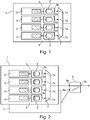
- Fig.1 represents an example of a diagram of an optical line card 1 of the state of the art.
- the optical line card 1 comprises a plurality of laser sources 3 (four in the present case) associated with a respective plurality of modulators 5 and an optical multiplexer 7 having a plurality of inputs 7a linked to the output 5b of the respective plurality of modulators 5.
- a second optical line card 1' as protection optical line card as disclosed in Fig.2 .
- the protection line card 1' is identical to the first optical line card 1 and is used in case of failure in the first optical line card 1.
- the output of both optical line cards 1 and 1' are linked to a protection switch 9 comprising two inputs 9a and one output 9b and capable of linking its output 9b to the first or the second input 9a.
- the protection switch 9 is switched to its second state and the protection optical line card 1' is used.
- both optical line card must be fully equipped to provide protection even if the failure occurs only on one element of the optical line card.
- the optical line card cannot be upgraded to a higher number of channels (for example in case of an increase of traffic so that the optical line card must be replaced by another optical line card having a higher capacity (comprising more than four channels in the present case).
- the invention aims to remedy all or some of the disadvantages of the above identified prior art.
- the present invention that particularly offers a modular and low cost solution, refers to an optical line card comprising:
- the optical line card also comprises a processing unit configured for controlling the configuration of the first and the second optical switches.
- the processing unit is configured for controlling the configuration of the first and the second optical switches according to the state of the first and the second tunable laser, the state of the first and the second modulators and from received control signals.
- control signals are sent by a network control plane unit.
- the elements of the optical line card are implemented in an integrated circuit.
- the second optical switch comprises a reflection mode wherein the signals received on its first and its second inputs are transmitted toward its second input.
- the first and the second optical circulators comprise a third input/output port.
- the present invention also refers to an optical transmitter comprising at least a first and a second optical line cards as described previously wherein the third input/output port of the second optical circulator of an optical line card is configured to be linked to the third input/output port of the first optical circulator of the next optical line card.
- the tunable lasers are tuned to different wavelengths from each other, the first optical switches are configured to link their first input to their first output, the second optical switch of the optical line cards except the last optical line card are set in a reflection mode and the second optical switch of the last optical line card is configured to transmit the multiplexed signal on its first output.
- some elements can be indexed such as a first element and a second element. In such case, it refers to a simple indexing to differentiate and name elements having similar functions. Such indexing does not imply any priority of one element with respect to another or a temporal order.
- Fig.3 represent an optical line card 10 comprising a first 12 and a second 12' tunable lasers which can be implemented in a common module or common integrated circuit or in two different modules.
- the respective outputs of the first 12 and the second 12' tunable lasers are coupled to a first 14a and a second 14a' inputs of a first optical switch 14.
- the first optical switch 14 is a 2*2 optical switch also called cross-bar type switch with two inputs 14a and 14a' and two outputs 14b and 14b', the optical switch 14 being able to transmit a signal received on an input 14a, 14a' to the first output 14b or to the second output 14b' (it is also possible to transmit toward both the first 14b and the second 14b' output) or to block a signal received on an input 14a, 14a'.
- the outputs 14b and 14b' of the first optical switch 14 are respectively coupled to a first modulator 16 via a first input 16a and to a second modulator 16' via a second input 16'a.
- the two modulators 16, 16' may be implemented on a common module, for example a dual modulation unit 15 corresponding to a common integrated circuit or on two separated modules.
- the modulators 16, 16' are configured for receiving an optical signal from one of the tunable lasers 12, 12' corresponding to a carrier signal and data signal from a data processing unit 17 and for modulating the carrier signal according to the data signal.
- the data processing unit 17 may be connected to a network control plan unit 19 such as a Software Defined Network (SDN) agent.
- SDN Software Defined Network
- the data processing unit 17 may be implemented within the optical line card 10.
- the network control plane unit 19 can be implemented in the same module as the data processing unit 17 or in a separated module.
- the network control plane unit 19 can be embedded in a microprocessor or a Field-Programable Gate Array (FPGA).
- the network control plane unit 19 is for example connected to a software defined network (SDN) controller.
- SDN software defined network
- the outputs 16b and 16'b of the modulators 16 and 16' are respectively coupled to a first 18 and a second 18' optical circulators.
- Each circulator 18, 18' has for example three input/output ports noted herein 18a, 18b, 18c for the first circulator 18 and 18'a, 18'b, 18'c for the second circulator 18'.
- the first input/output ports 18a and 18'a are respectively coupled to the first 16 and the second 16' modulators and the second input/output ports 18b and 18'b are respectively coupled to a first 20a and a second 20a' inputs of a second optical switch 20.
- the optical circulators 18, 18' are configured for transmitting the signal received on their first input/ouput port 18a, 18'a toward its second input/output port 18b, 18'b.
- the second optical switch 20 is a 2*2 optical switch with two inputs 20a and 20a' and two outputs 20b and 20b', the optical switch 20 being able to transmit a signal received on an input 20a, 20a' to the first output 20b or to the second output 20b' (it is also possible to transmit toward both the first 20b and the second 20b' output).
- the second optical switch 20 is also configurable for reflecting back a signal received on its first 20a and/or its second 20a' inputs toward one of its inputs 20a, 20a', for example the second input 20a' in a reflection mode.
- the first 14 and the second 20 optical switches are for example driven by a processing unit (not represented). Such processing unit may be implemented together with the data processing unit 17 within the optical line card 10.
- the architecture of the optical line card 10 described in Fig.3 enables different configurations which allows an enhanced modularity. The different configurations will now be described.
- the optical line card 10 can be used to transmit two different signals to two different destinations, for example to two different egress nodes. Such transmission is achieved by configuring the first optical switch 14 to transmit the signals on its first 14a and its second 14a' inputs respectively to its first 14b and its second 14b' outputs. The two signals are therefore transmitted respectively to the first 16 and the second 16' modulators. The two modulated signals are then transmitted to the second optical switch 20 via respectively the first 18 and the second 18' optical circulators. The second optical switch 20 is configured for transmitting the signal received on its first input 20a toward its first output 20b and the signal received on its second input 20a' toward its second output 20b'. The two modulated signals may then be transmitted toward their respective destinations. Using n optical line cards 10 as described in Fig.4 enables therefore to create a sliceable transmitter capable of transmitting 2n optical signals toward 2n different destinations.
- the optical line card 10 can be used to transmit a single signal and for providing a protection in case of a failure of a tunable laser 12, for example or a modulator 16, for example, the second tunable laser 12' and the second modulator 16' are for example used as protection for the first tunable laser 12 and the first modulator 16. It is therefore supposed that the first tunable laser 12 and the first modulator 16 are used for the signal transmission.
- the optical line card 10 can be used to transmit a multiplexed signal comprising two different wavelength channels, also called 'super-channels', corresponding to the wavelength of the first 12 and the second 12' tunable lasers.
- the first optical switch 14 is configured to transmit the signal received on its first input 14a (linked to the first tunable laser 12) toward its first output 14b (linked to the first modulator 16) and to transmit the signal received on its second input 14a' (linked to the second tunable laser 12') toward its second output 14b' (linked to the second modulator 16').
- the second optical switch 20 is configured for transmitting the signal received on its first 20a and its second 20a' inputs toward its first output 20b so that the two signals transmitted by the first 16 and the second 16' modulators are multiplexed and transmitted to the first output 20b of the second optical switch 20.
- optical line cards 10 it is also possible to cascade the different optical line cards 10 in order to provide an upgrade of a transmitter 100, as represented in Fig. 8 .
- Such upgrade enables adding two additional channels (per added optical line card 10) in order to produce a multiplexed signal.
- the different optical line cards 10 are connected by their optical circulators 18 and 18'.
- the third input/output port 18'c of a second optical circulator 18' of a given optical line card 10 is linked to the third input/output port 18c of a first optical circulator 18 of a next optical line card 10 as represented in Fig.8 in the case of three cascaded optical line cards noted 10, 10' and 10".
- the third input/ouput port 18c of the first optical circulator 18 of the first optical line card 10 and the third input/output port 18'c of the second optical circulator 18' of the last optical line card 10" are not used.
- the different tunable lasers of the cascaded optical line cards 10, 10' and 10" are tuned to the different frequencies corresponding to the central frequency of each channel of the multiplexed signal.
- the first optical switches 14 are configured to transmit the signals received on their respective inputs 14a and 14a' toward their respective outputs 14b and 14b'.
- the signals provided by the respective first 12 and second 12' tunable lasers are then modulated by the respective first 16 and second 16' modulators.
- the first optical circulators 18 of the optical line cards 10' and 10" are configured for transmitting the signals received on their first 18a and third 18c input/output ports toward their second input/output port 18b.
- the first optical circulator 18 of the first optical line card 10 is configured for transmitting the signal received on its first input/output port 18a toward its second input/output port 18b.
- the second optical circulators 18' of the optical line cards 10, 10' are configured for transmitting the signals received on their first input/output port 18'a toward their second input/output port 18'b and for transmitting the signals received on their second input/output port 18'b toward their third input/output port 18'c.
- the second optical circulator 18' of the last optical line card 10" is configured for transmitting the signal received on its first input/output port 18'a toward its second input/output port 18'b.
- the second optical switches 20 of the optical line cards 10, 10' are configured in the reflection mode so that the signals received on the first 20a and the second 20a' inputs of the second optical switches 20 are transmitted to their second input 20a'.
- the second optical switch 20 of the last optical line card 10" is configured for transmitting the signals received on its first 20a and second 20a' inputs toward its first output 20b.
- the two signals provided by an optical line card 10, 10', 10" are multiplexed with the signals provided by the other optical line cards 10, 10', 10".
- the number n of cascaded optical line cards 10 enables to obtain a multiplexed signal comprising 2n channels.
- the multiplexed signal transmitted from one optical line card to the next is represented and the signal obtained at the first output 20b of the last optical line card 10" comprises six channels as three different optical line cards 10, 10' and 10" are cascaded in this example.
- the architecture of the optical line cards 10 presented previously enables obtaining different functions depending on the configuration of the optical line card 10 and provides therefore a great modularity with a limited number of elements. Furthermore, it is easy to combine several optical line cards 10 in order to obtain an upgraded transmitter 100 with a higher capacity or with additional protection or capacity.
- the present invention also refers to an optical transmitter 100 comprising at least one optical line card 10 as described previously.
- the transmitter 100 may also comprise a data processing unit 17, which can also be implemented within the optical line card 10.
- the third input/output port 18'c of the second optical circulator 18' of an optical line card 10 is configured to be linked to the third input/output 18c of the first optical circulator 18 of the next optical line card 10.
- processors may be provided through the use of dedicated hardware as well as hardware capable of executing software in association with appropriate software.
- the functions may be provided by a single dedicated processor, by a single shared processor, or by a plurality of individual processors, some of which may be shared.
- processor or “controller” should not be construed to refer exclusively to hardware capable of executing software, and may implicitly include, without limitation, digital signal processor (DSP) hardware, network processor, application specific integrated circuit (ASIC), field programmable gate array (FPGA), read only memory (ROM) for storing software, random access memory (RAM), and non volatile storage.
- DSP digital signal processor
- ASIC application specific integrated circuit
- FPGA field programmable gate array
- ROM read only memory
- RAM random access memory
- non volatile storage Other hardware, conventional and/or custom, may also be included.
- any switches shown in the FIGS. are conceptual only. Their function may be carried out through the operation of program logic, through dedicated logic, through the interaction of program control and dedicated logic, or even manually, the particular technique being selectable by the implementer as more specifically understood from the context.
- the presented optical line card may be implemented in a photonic integrated circuit (PIC) and the optical switch may be implemented as micro opto electro mechanical system (MEMS).
- PIC photonic integrated circuit
- MEMS micro opto electro mechanical system
Landscapes
- Engineering & Computer Science (AREA)
- Computer Networks & Wireless Communication (AREA)
- Optical Communication System (AREA)
Abstract
Description
- The present invention relates to the field of communication networks and more precisely of optical line cards used in optical transmission.
- Optical line card are known to gather the different elements required for transmitting a multiplexed optical signal.
Fig.1 represents an example of a diagram of an optical line card 1 of the state of the art. The optical line card 1 comprises a plurality of laser sources 3 (four in the present case) associated with a respective plurality ofmodulators 5 and anoptical multiplexer 7 having a plurality ofinputs 7a linked to theoutput 5b of the respective plurality ofmodulators 5. - Furthermore, in order to overcome any failure of an element of the optical line card 1 which could lead to an interruption of the transmission of the optical signals, it is also known to use a second optical line card 1' as protection optical line card as disclosed in
Fig.2 . The protection line card 1' is identical to the first optical line card 1 and is used in case of failure in the first optical line card 1. To achieve this, the output of both optical line cards 1 and 1' are linked to aprotection switch 9 comprising twoinputs 9a and oneoutput 9b and capable of linking itsoutput 9b to the first or thesecond input 9a. Thus, in case of a failure in the first optical line card 1, theprotection switch 9 is switched to its second state and the protection optical line card 1' is used. - However, such configuration is expensive and lacks modularity. Indeed, both optical line card must be fully equipped to provide protection even if the failure occurs only on one element of the optical line card. Moreover, the optical line card cannot be upgraded to a higher number of channels (for example in case of an increase of traffic so that the optical line card must be replaced by another optical line card having a higher capacity (comprising more than four channels in the present case).
- It is then needed to have a better solution with higher modularity and lower cost.
- The invention aims to remedy all or some of the disadvantages of the above identified prior art. The present invention that particularly offers a modular and low cost solution, refers to an optical line card comprising:
- a first tunable laser ,
- a second tunable laser,
- a first optical switch comprising a first input linked to the first tunable laser, a second input linked to the second tunable laser, a first output which can be linked to the first or to the second input, a second output which can be linked to the first or to the second input,
- a dual modulation unit comprising:
- a first modulator configured for modulating a first signal received on a first input linked to the first output of the first optical switch, the first modulated signal being transmitted to a first output,
- a second modulator configured for modulating a second signal received on a second input linked to the second output of the first optical switch, the second modulated signal being transmitted to a second output,
- a first optical circulator comprising a first input/output port linked to the first output of the dual modulation unit and a second input/output port,
- a second optical circulator comprising a first input/output port linked to the second output of the dual modulation unit and a second input/output port,
- a second optical switch comprising a first input linked to the second input/output port of the first optical circulator and a second input linked to the second input/output port of the second optical circulator.
- According to another aspect of the present invention, the optical line card also comprises a processing unit configured for controlling the configuration of the first and the second optical switches.
- According to another aspect of the present invention, the processing unit is configured for controlling the configuration of the first and the second optical switches according to the state of the first and the second tunable laser, the state of the first and the second modulators and from received control signals.
- According to another aspect of the present invention, the control signals are sent by a network control plane unit.
- According to another aspect of the present invention, the elements of the optical line card are implemented in an integrated circuit.
- According to another aspect of the present invention, the second optical switch comprises a reflection mode wherein the signals received on its first and its second inputs are transmitted toward its second input.
- According to another aspect of the present invention, the first and the second optical circulators comprise a third input/output port.
- The present invention also refers to an optical transmitter comprising at least a first and a second optical line cards as described previously wherein the third input/output port of the second optical circulator of an optical line card is configured to be linked to the third input/output port of the first optical circulator of the next optical line card.
- According to another aspect of the present invention, to produce an output signal corresponding to a wavelength division multiplexing signal, the tunable lasers are tuned to different wavelengths from each other, the first optical switches are configured to link their first input to their first output, the second optical switch of the optical line cards except the last optical line card are set in a reflection mode and the second optical switch of the last optical line card is configured to transmit the multiplexed signal on its first output.
-
-
FIG.1 is a diagram of an optical line card according to the state of the art, -
FIG.2 is a diagram of a transmitter comprising a first optical line card and a protection optical line card according to the state of the art, -
FIG.3 is a diagram of an optical line card according to the present invention, -
FIG.4 is a diagram of a first configuration of an optical line card according to the present invention, -
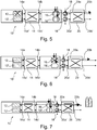
FIG.5 is a diagram of a second configuration of an optical line card according to the present invention; -
FIG.6 is a diagram of a third configuration of an optical line card according to the present invention; -
FIG.7 is a diagram of a fourth configuration of an optical line card according to the present invention; -
FIG.8 is a diagram of a transmitter comprising a plurality of optical line cards according to the present invention; - The following embodiments are examples. Although the description refers to one or several embodiments, it does not mean necessarily that the features apply only to a single embodiment. Simple features of the different embodiments may be combined to provide additional embodiments.
- In the following description, some elements can be indexed such as a first element and a second element. In such case, it refers to a simple indexing to differentiate and name elements having similar functions. Such indexing does not imply any priority of one element with respect to another or a temporal order.
-
Fig.3 represent anoptical line card 10 comprising a first 12 and a second 12' tunable lasers which can be implemented in a common module or common integrated circuit or in two different modules. The respective outputs of the first 12 and the second 12' tunable lasers are coupled to a first 14a and a second 14a' inputs of a firstoptical switch 14. The firstoptical switch 14 is a 2*2 optical switch also called cross-bar type switch with twoinputs outputs optical switch 14 being able to transmit a signal received on aninput first output 14b or to thesecond output 14b' (it is also possible to transmit toward both the first 14b and the second 14b' output) or to block a signal received on aninput outputs optical switch 14 are respectively coupled to afirst modulator 16 via afirst input 16a and to a second modulator 16' via a second input 16'a. The twomodulators 16, 16' may be implemented on a common module, for example adual modulation unit 15 corresponding to a common integrated circuit or on two separated modules. Themodulators 16, 16' are configured for receiving an optical signal from one of thetunable lasers 12, 12' corresponding to a carrier signal and data signal from a data processing unit 17 and for modulating the carrier signal according to the data signal. The data processing unit 17 may be connected to a networkcontrol plan unit 19 such as a Software Defined Network (SDN) agent. The data processing unit 17 may be implemented within theoptical line card 10. The networkcontrol plane unit 19 can be implemented in the same module as the data processing unit 17 or in a separated module. The networkcontrol plane unit 19 can be embedded in a microprocessor or a Field-Programable Gate Array (FPGA). The networkcontrol plane unit 19 is for example connected to a software defined network (SDN) controller.
Theoutputs 16b and 16'b of themodulators 16 and 16' are respectively coupled to a first 18 and a second 18' optical circulators. Eachcirculator 18, 18' has for example three input/output ports noted herein 18a, 18b, 18c for thefirst circulator 18 and 18'a, 18'b, 18'c for the second circulator 18'. The first input/output ports 18a and 18'a are respectively coupled to the first 16 and the second 16' modulators and the second input/output ports 18b and 18'b are respectively coupled to a first 20a and a second 20a' inputs of a secondoptical switch 20. Theoptical circulators 18, 18' are configured for transmitting the signal received on their first input/ouput port 18a, 18'a toward its second input/output port 18b, 18'b. The secondoptical switch 20 is a 2*2 optical switch with twoinputs outputs optical switch 20 being able to transmit a signal received on aninput first output 20b or to thesecond output 20b' (it is also possible to transmit toward both the first 20b and the second 20b' output). The secondoptical switch 20 is also configurable for reflecting back a signal received on its first 20a and/or its second 20a' inputs toward one of itsinputs second input 20a' in a reflection mode. The first 14 and the second 20 optical switches are for example driven by a processing unit (not represented). Such processing unit may be implemented together with the data processing unit 17 within theoptical line card 10. - The architecture of the
optical line card 10 described inFig.3 enables different configurations which allows an enhanced modularity. The different configurations will now be described. - According to a first configuration represented in
Fig.4 , theoptical line card 10 can be used to transmit two different signals to two different destinations, for example to two different egress nodes. Such transmission is achieved by configuring the firstoptical switch 14 to transmit the signals on its first 14a and its second 14a' inputs respectively to its first 14b and its second 14b' outputs. The two signals are therefore transmitted respectively to the first 16 and the second 16' modulators. The two modulated signals are then transmitted to the secondoptical switch 20 via respectively the first 18 and the second 18' optical circulators. The secondoptical switch 20 is configured for transmitting the signal received on itsfirst input 20a toward itsfirst output 20b and the signal received on itssecond input 20a' toward itssecond output 20b'. The two modulated signals may then be transmitted toward their respective destinations. Using noptical line cards 10 as described inFig.4 enables therefore to create a sliceable transmitter capable of transmitting 2n optical signals toward 2n different destinations. - According to a second configuration represented in
Figs.5 and 6 , theoptical line card 10 can be used to transmit a single signal and for providing a protection in case of a failure of atunable laser 12, for example or amodulator 16, for example, the second tunable laser 12' and the second modulator 16' are for example used as protection for the firsttunable laser 12 and thefirst modulator 16. It is therefore supposed that the firsttunable laser 12 and thefirst modulator 16 are used for the signal transmission. - a) Tunable laser protection
In case of a failure of the firsttunable laser 12 as represented inFig.5 by the cross, the second tunable laser 12' is activated and set as the same frequency as the firsttunable laser 12. The firstoptical switch 14 is configured for transmitting the signal received on itssecond input 14a' (linked to the second tunable laser 12') toward itsfirst output 14b (linked to the first modulator 16) and the secondoptical switch 20 is configured for transmitting the signal received on itsfirst input 20a (linked to thefirst modulator 16 via the first optical circulator 18) toward itsfirst output 20b. - b) Modulator protection
In case of failure of thefirst modulator 16 as represented by the cross inFig.6 , the firstoptical switch 14 is configured for transmitting the signal received on itsfirst input 14a (linked to the first tunable laser 12) toward itssecond output 14b' (linked to the second modulator 16') so that the signal provided by the firsttunable laser 12 is transmitted to the second modulator 16'. The secondoptical switch 20 is configured for transmitting the signal received on itssecond input 20a' (linked to the second modulator 16' via the second optical circulator 18') toward itsfirst output 20b. - c) In the same way, in case of failure of both the first
tunable laser 12 and thefirst modulator 16, the first 14 and the second 20 optical switches can be configured so that the second tunable laser 12' and the second modulator 16' are used for the signal transmission of the signal. - According to a third configuration represented in
Fig.7 , theoptical line card 10 can be used to transmit a multiplexed signal comprising two different wavelength channels, also called 'super-channels', corresponding to the wavelength of the first 12 and the second 12' tunable lasers. The firstoptical switch 14 is configured to transmit the signal received on itsfirst input 14a (linked to the first tunable laser 12) toward itsfirst output 14b (linked to the first modulator 16) and to transmit the signal received on itssecond input 14a' (linked to the second tunable laser 12') toward itssecond output 14b' (linked to the second modulator 16'). The secondoptical switch 20 is configured for transmitting the signal received on its first 20a and its second 20a' inputs toward itsfirst output 20b so that the two signals transmitted by the first 16 and the second 16' modulators are multiplexed and transmitted to thefirst output 20b of the secondoptical switch 20. - Using several
optical line cards 10, it is also possible to cascade the differentoptical line cards 10 in order to provide an upgrade of atransmitter 100, as represented inFig. 8 . Such upgrade enables adding two additional channels (per added optical line card 10) in order to produce a multiplexed signal. In order to obtain such result, the differentoptical line cards 10 are connected by theiroptical circulators 18 and 18'. - The third input/output port 18'c of a second optical circulator 18' of a given
optical line card 10 is linked to the third input/output port 18c of a firstoptical circulator 18 of a nextoptical line card 10 as represented inFig.8 in the case of three cascaded optical line cards noted 10, 10' and 10". In such configuration, the third input/ouput port 18c of the firstoptical circulator 18 of the firstoptical line card 10 and the third input/output port 18'c of the second optical circulator 18' of the lastoptical line card 10" are not used. - In order to produce a multiplexed signal comprising a plurality of neighbouring channels, the different tunable lasers of the cascaded
optical line cards - The first
optical switches 14 are configured to transmit the signals received on theirrespective inputs respective outputs - The first
optical circulators 18 of theoptical line cards 10' and 10" (except for the first optical line card 10) are configured for transmitting the signals received on their first 18a and third 18c input/output ports toward their second input/output port 18b. The firstoptical circulator 18 of the firstoptical line card 10 is configured for transmitting the signal received on its first input/output port 18a toward its second input/output port 18b. - The second optical circulators 18' of the
optical line cards 10, 10' (except for the lastoptical line card 10") are configured for transmitting the signals received on their first input/output port 18'a toward their second input/output port 18'b and for transmitting the signals received on their second input/output port 18'b toward their third input/output port 18'c. The second optical circulator 18' of the lastoptical line card 10" is configured for transmitting the signal received on its first input/output port 18'a toward its second input/output port 18'b. - The second
optical switches 20 of theoptical line cards 10, 10' (except for the lastoptical line card 10") are configured in the reflection mode so that the signals received on the first 20a and the second 20a' inputs of the secondoptical switches 20 are transmitted to theirsecond input 20a'. The secondoptical switch 20 of the lastoptical line card 10" is configured for transmitting the signals received on its first 20a and second 20a' inputs toward itsfirst output 20b. - Thus, with such configuration, the two signals provided by an
optical line card optical line cards optical line cards 10 enables to obtain a multiplexed signal comprising 2n channels. InFig.7 , the multiplexed signal transmitted from one optical line card to the next is represented and the signal obtained at thefirst output 20b of the lastoptical line card 10" comprises six channels as three differentoptical line cards - It is also possible to combine the different configurations presented previously, for example to obtained a multiplexed signal combined with protection of some or all different channels (a higher number of
optical line cards 10 is then required to obtain the same number of channels). Any number ofoptical line cards 10 can be combined. - Thus, the architecture of the
optical line cards 10 presented previously enables obtaining different functions depending on the configuration of theoptical line card 10 and provides therefore a great modularity with a limited number of elements. Furthermore, it is easy to combine severaloptical line cards 10 in order to obtain an upgradedtransmitter 100 with a higher capacity or with additional protection or capacity. - The present invention also refers to an
optical transmitter 100 comprising at least oneoptical line card 10 as described previously. Thetransmitter 100 may also comprise a data processing unit 17, which can also be implemented within theoptical line card 10. In the case of anoptical transmitter 100 comprising severaloptical line cards 10, the third input/output port 18'c of the second optical circulator 18' of anoptical line card 10 is configured to be linked to the third input/output 18c of the firstoptical circulator 18 of the nextoptical line card 10. - The functions of the various elements shown in the Figs., including any functional blocks labeled as "processors" or "processing units", may be provided through the use of dedicated hardware as well as hardware capable of executing software in association with appropriate software. When provided by a processor, the functions may be provided by a single dedicated processor, by a single shared processor, or by a plurality of individual processors, some of which may be shared. Moreover, explicit use of the term "processor" or "controller" should not be construed to refer exclusively to hardware capable of executing software, and may implicitly include, without limitation, digital signal processor (DSP) hardware, network processor, application specific integrated circuit (ASIC), field programmable gate array (FPGA), read only memory (ROM) for storing software, random access memory (RAM), and non volatile storage. Other hardware, conventional and/or custom, may also be included. Similarly, any switches shown in the FIGS. are conceptual only. Their function may be carried out through the operation of program logic, through dedicated logic, through the interaction of program control and dedicated logic, or even manually, the particular technique being selectable by the implementer as more specifically understood from the context.
- In particular, the presented optical line card may be implemented in a photonic integrated circuit (PIC) and the optical switch may be implemented as micro opto electro mechanical system (MEMS).
Claims (9)
- Optical line card (10, 10', 10") comprising:- a first tunable laser (12),- a second tunable laser (12'),- a first optical switch (14) comprising a first input (14a) linked to the first tunable laser (12), a second input (14a') linked to the second tunable laser (12'), a first output (14b) which can be linked to the first (14a) or to the second (14a') input, a second output (14b') which can be linked to the first (14a) or to the second (14a') input,- a dual modulation unit (15) comprising:- a first modulator (16) configured for modulating a first signal received on a first input (16a) linked to the first output (14b) of the first optical switch (14), the first modulated signal being transmitted to a first output (16b),- a second modulator (16') configured for modulating a second signal received on a second input (16'a) linked to the second output (14b') of the first optical switch (14), the second modulated signal being transmitted to a second output (16'b),- a first optical circulator (18) comprising a first input/output port (18a) linked to the first output (16b) of the dual modulation unit (15) and a second input/output port (18b),- a second optical circulator (18') comprising a first input/output port (18'a) linked to the second output (16'b) of the dual modulation unit (15) and a second input/output port (18'b),- a second optical switch (20) comprising a first input (20a) linked to the second input/output port (18b) of the first optical circulator (18) and a second input (20a') linked to the second input/output port (18'b) of the second optical circulator (18').
- Optical line card (10, 10', 10") in accordance with claim 1 also comprising a processing unit configured for controlling the configuration of the first (14) and the second (20) optical switches.
- Optical line card (10, 10', 10") in accordance with claim 2 wherein the processing unit is configured for controlling the configuration of the first (14) and the second (20) optical switches according to the state of the first (12) and the second (12') tunable laser, the state of the first (16) and the second (16') modulators and from received control signals.
- Optical line card (10, 10', 10") in accordance with claims 3 wherein the control signals are sent by a network control plane unit (19).
- Optical line card (10, 10', 10") in accordance with one of the previous claims wherein the elements of the optical line card (10) are implemented in an integrated circuit.
- Optical line card (10, 10', 10") in accordance with one of the previous claims wherein the second optical switch (20) comprises a reflection mode wherein the signals received on its first (20a) and its second (20a') inputs are transmitted toward its second input (20a').
- Optical line card (10, 10', 10") in accordance with one of the previous claims wherein the first (18) and the second (18') optical circulators comprise a third input/output port (18c, 18'c).
- Optical transmitter (100) comprising at least a first (10) and a second (10') optical line cards in accordance with claims 7 wherein the third input/output port (18'c) of the second optical circulator (18') of an optical line card (10) is configured to be linked to the third input/output port (18c) of the first optical circulator (18) of the next optical line card (10').
- Optical transmitter (100) in accordance with claim 8 in combination with claim 6 wherein to produce an output signal corresponding to a wavelength division multiplexing signal, the tunable lasers (12, 12') are tuned to different wavelengths from each other, the first optical switches (14) are configured to link their first input (14a) to their first output (14b), the second optical switch (20) of the optical line cards (10, 10') except the last optical line card (10") are set in a reflection mode and the second optical switch (20) of the last optical line card (10") is configured to transmit the multiplexed signal on its first output (20b).
Priority Applications (1)
| Application Number | Priority Date | Filing Date | Title |
|---|---|---|---|
| EP17305721.7A EP3416316B1 (en) | 2017-06-14 | 2017-06-14 | Optical line card and transmitter |
Applications Claiming Priority (1)
| Application Number | Priority Date | Filing Date | Title |
|---|---|---|---|
| EP17305721.7A EP3416316B1 (en) | 2017-06-14 | 2017-06-14 | Optical line card and transmitter |
Publications (2)
| Publication Number | Publication Date |
|---|---|
| EP3416316A1 true EP3416316A1 (en) | 2018-12-19 |
| EP3416316B1 EP3416316B1 (en) | 2019-09-25 |
Family
ID=59227672
Family Applications (1)
| Application Number | Title | Priority Date | Filing Date |
|---|---|---|---|
| EP17305721.7A Active EP3416316B1 (en) | 2017-06-14 | 2017-06-14 | Optical line card and transmitter |
Country Status (1)
| Country | Link |
|---|---|
| EP (1) | EP3416316B1 (en) |
Citations (1)
| Publication number | Priority date | Publication date | Assignee | Title |
|---|---|---|---|---|
| US20010013963A1 (en) * | 2000-02-01 | 2001-08-16 | Mathias Bischoff | Access node for optical networks with variable-access wavelengths, user device for connection to such an access node, method for feeding a number of signals from a number of users into an optical network and using an access node and at least one user device for carrying out such a method |
-
2017
- 2017-06-14 EP EP17305721.7A patent/EP3416316B1/en active Active
Patent Citations (1)
| Publication number | Priority date | Publication date | Assignee | Title |
|---|---|---|---|---|
| US20010013963A1 (en) * | 2000-02-01 | 2001-08-16 | Mathias Bischoff | Access node for optical networks with variable-access wavelengths, user device for connection to such an access node, method for feeding a number of signals from a number of users into an optical network and using an access node and at least one user device for carrying out such a method |
Also Published As
| Publication number | Publication date |
|---|---|
| EP3416316B1 (en) | 2019-09-25 |
Similar Documents
| Publication | Publication Date | Title |
|---|---|---|
| EP2564532B1 (en) | Reconfigurable optical add drop multiplexer node automated topology discovery systems and methods | |
| US9160478B2 (en) | Reconfigurable optical add/drop multiplexor and optical switching node | |
| EP0668674A2 (en) | Optical wavelength division multiplexed network system | |
| US8699877B2 (en) | Wavelength division multiplex terminal with automatic configuration and supervision of switch connections | |
| US9742519B2 (en) | Photonic cross-connect with reconfigurable add-drop-functionality | |
| US11652563B2 (en) | Optical demultiplexer, optical separation device, optical transmission system, and optical transmission method | |
| EP2913943A1 (en) | Optical communication with spatially multiplexed optical packet signals | |
| EP2982066B1 (en) | Optical switch | |
| US10530515B2 (en) | OADM node and method in WDM system | |
| US20210219031A1 (en) | Optical cross-connect device | |
| EP2615755B1 (en) | Optical switching node for a WDM optical network | |
| EP2333995B1 (en) | Optical switch router | |
| EP1407568B1 (en) | Wdm ring network for flexible connections | |
| EP2426841B1 (en) | Optical add and/or drop device for an optical network element | |
| EP3416316B1 (en) | Optical line card and transmitter | |
| EP2963851B1 (en) | A multidirectional optical apparatus | |
| EP2651059B1 (en) | Add device and drop device for an optical network element | |
| US20230199350A1 (en) | Optical switching device, optical switching system, and method of optical switching | |
| EP1665867B1 (en) | Node for an optical communication network | |
| JP6738311B2 (en) | Network node | |
| JP2019015833A (en) | Wavelength selective switch module | |
| EP2403170B1 (en) | A reconfigurable optical add and drop wavelength multiplexer for an optical network using wavelength division multiplexing | |
| EP3299856A1 (en) | Photonic integrated chip device having a common optical edge interface | |
| EP2773057A1 (en) | Optical network node and method of transmitting wavelength multiplexed optical data signals | |
| EP2720394A1 (en) | Multidirectional add and drop devices for a WDM optical network |
Legal Events
| Date | Code | Title | Description |
|---|---|---|---|
| PUAI | Public reference made under article 153(3) epc to a published international application that has entered the european phase |
Free format text: ORIGINAL CODE: 0009012 |
|
| STAA | Information on the status of an ep patent application or granted ep patent |
Free format text: STATUS: REQUEST FOR EXAMINATION WAS MADE |
|
| 17P | Request for examination filed |
Effective date: 20180405 |
|
| AK | Designated contracting states |
Kind code of ref document: A1 Designated state(s): AL AT BE BG CH CY CZ DE DK EE ES FI FR GB GR HR HU IE IS IT LI LT LU LV MC MK MT NL NO PL PT RO RS SE SI SK SM TR |
|
| AX | Request for extension of the european patent |
Extension state: BA ME |
|
| GRAP | Despatch of communication of intention to grant a patent |
Free format text: ORIGINAL CODE: EPIDOSNIGR1 |
|
| STAA | Information on the status of an ep patent application or granted ep patent |
Free format text: STATUS: GRANT OF PATENT IS INTENDED |
|
| INTG | Intention to grant announced |
Effective date: 20190418 |
|
| RBV | Designated contracting states (corrected) |
Designated state(s): AL AT BE BG CH CY CZ DE DK EE ES FI FR GB GR HR HU IE IS IT LI LT LU LV MC MK MT NL NO PL PT RO RS SE SI SK SM TR |
|
| GRAS | Grant fee paid |
Free format text: ORIGINAL CODE: EPIDOSNIGR3 |
|
| GRAA | (expected) grant |
Free format text: ORIGINAL CODE: 0009210 |
|
| STAA | Information on the status of an ep patent application or granted ep patent |
Free format text: STATUS: THE PATENT HAS BEEN GRANTED |
|
| RAP1 | Party data changed (applicant data changed or rights of an application transferred) |
Owner name: NOKIA SOLUTIONS AND NETWORKS OY |
|
| AK | Designated contracting states |
Kind code of ref document: B1 Designated state(s): AL AT BE BG CH CY CZ DE DK EE ES FI FR GB GR HR HU IE IS IT LI LT LU LV MC MK MT NL NO PL PT RO RS SE SI SK SM TR |
|
| REG | Reference to a national code |
Ref country code: GB Ref legal event code: FG4D |
|
| REG | Reference to a national code |
Ref country code: CH Ref legal event code: EP |
|
| REG | Reference to a national code |
Ref country code: AT Ref legal event code: REF Ref document number: 1184848 Country of ref document: AT Kind code of ref document: T Effective date: 20191015 |
|
| REG | Reference to a national code |
Ref country code: IE Ref legal event code: FG4D |
|
| REG | Reference to a national code |
Ref country code: DE Ref legal event code: R096 Ref document number: 602017007315 Country of ref document: DE |
|
| REG | Reference to a national code |
Ref country code: NL Ref legal event code: MP Effective date: 20190925 |
|
| PG25 | Lapsed in a contracting state [announced via postgrant information from national office to epo] |
Ref country code: NO Free format text: LAPSE BECAUSE OF FAILURE TO SUBMIT A TRANSLATION OF THE DESCRIPTION OR TO PAY THE FEE WITHIN THE PRESCRIBED TIME-LIMIT Effective date: 20191225 Ref country code: FI Free format text: LAPSE BECAUSE OF FAILURE TO SUBMIT A TRANSLATION OF THE DESCRIPTION OR TO PAY THE FEE WITHIN THE PRESCRIBED TIME-LIMIT Effective date: 20190925 Ref country code: HR Free format text: LAPSE BECAUSE OF FAILURE TO SUBMIT A TRANSLATION OF THE DESCRIPTION OR TO PAY THE FEE WITHIN THE PRESCRIBED TIME-LIMIT Effective date: 20190925 Ref country code: SE Free format text: LAPSE BECAUSE OF FAILURE TO SUBMIT A TRANSLATION OF THE DESCRIPTION OR TO PAY THE FEE WITHIN THE PRESCRIBED TIME-LIMIT Effective date: 20190925 Ref country code: BG Free format text: LAPSE BECAUSE OF FAILURE TO SUBMIT A TRANSLATION OF THE DESCRIPTION OR TO PAY THE FEE WITHIN THE PRESCRIBED TIME-LIMIT Effective date: 20191225 Ref country code: LT Free format text: LAPSE BECAUSE OF FAILURE TO SUBMIT A TRANSLATION OF THE DESCRIPTION OR TO PAY THE FEE WITHIN THE PRESCRIBED TIME-LIMIT Effective date: 20190925 |
|
| REG | Reference to a national code |
Ref country code: LT Ref legal event code: MG4D |
|
| PG25 | Lapsed in a contracting state [announced via postgrant information from national office to epo] |
Ref country code: LV Free format text: LAPSE BECAUSE OF FAILURE TO SUBMIT A TRANSLATION OF THE DESCRIPTION OR TO PAY THE FEE WITHIN THE PRESCRIBED TIME-LIMIT Effective date: 20190925 Ref country code: GR Free format text: LAPSE BECAUSE OF FAILURE TO SUBMIT A TRANSLATION OF THE DESCRIPTION OR TO PAY THE FEE WITHIN THE PRESCRIBED TIME-LIMIT Effective date: 20191226 Ref country code: RS Free format text: LAPSE BECAUSE OF FAILURE TO SUBMIT A TRANSLATION OF THE DESCRIPTION OR TO PAY THE FEE WITHIN THE PRESCRIBED TIME-LIMIT Effective date: 20190925 |
|
| REG | Reference to a national code |
Ref country code: AT Ref legal event code: MK05 Ref document number: 1184848 Country of ref document: AT Kind code of ref document: T Effective date: 20190925 |
|
| PG25 | Lapsed in a contracting state [announced via postgrant information from national office to epo] |
Ref country code: RO Free format text: LAPSE BECAUSE OF FAILURE TO SUBMIT A TRANSLATION OF THE DESCRIPTION OR TO PAY THE FEE WITHIN THE PRESCRIBED TIME-LIMIT Effective date: 20190925 Ref country code: PT Free format text: LAPSE BECAUSE OF FAILURE TO SUBMIT A TRANSLATION OF THE DESCRIPTION OR TO PAY THE FEE WITHIN THE PRESCRIBED TIME-LIMIT Effective date: 20200127 Ref country code: PL Free format text: LAPSE BECAUSE OF FAILURE TO SUBMIT A TRANSLATION OF THE DESCRIPTION OR TO PAY THE FEE WITHIN THE PRESCRIBED TIME-LIMIT Effective date: 20190925 Ref country code: ES Free format text: LAPSE BECAUSE OF FAILURE TO SUBMIT A TRANSLATION OF THE DESCRIPTION OR TO PAY THE FEE WITHIN THE PRESCRIBED TIME-LIMIT Effective date: 20190925 Ref country code: AL Free format text: LAPSE BECAUSE OF FAILURE TO SUBMIT A TRANSLATION OF THE DESCRIPTION OR TO PAY THE FEE WITHIN THE PRESCRIBED TIME-LIMIT Effective date: 20190925 Ref country code: NL Free format text: LAPSE BECAUSE OF FAILURE TO SUBMIT A TRANSLATION OF THE DESCRIPTION OR TO PAY THE FEE WITHIN THE PRESCRIBED TIME-LIMIT Effective date: 20190925 Ref country code: EE Free format text: LAPSE BECAUSE OF FAILURE TO SUBMIT A TRANSLATION OF THE DESCRIPTION OR TO PAY THE FEE WITHIN THE PRESCRIBED TIME-LIMIT Effective date: 20190925 Ref country code: AT Free format text: LAPSE BECAUSE OF FAILURE TO SUBMIT A TRANSLATION OF THE DESCRIPTION OR TO PAY THE FEE WITHIN THE PRESCRIBED TIME-LIMIT Effective date: 20190925 Ref country code: IT Free format text: LAPSE BECAUSE OF FAILURE TO SUBMIT A TRANSLATION OF THE DESCRIPTION OR TO PAY THE FEE WITHIN THE PRESCRIBED TIME-LIMIT Effective date: 20190925 |
|
| PG25 | Lapsed in a contracting state [announced via postgrant information from national office to epo] |
Ref country code: CZ Free format text: LAPSE BECAUSE OF FAILURE TO SUBMIT A TRANSLATION OF THE DESCRIPTION OR TO PAY THE FEE WITHIN THE PRESCRIBED TIME-LIMIT Effective date: 20190925 Ref country code: SM Free format text: LAPSE BECAUSE OF FAILURE TO SUBMIT A TRANSLATION OF THE DESCRIPTION OR TO PAY THE FEE WITHIN THE PRESCRIBED TIME-LIMIT Effective date: 20190925 Ref country code: SK Free format text: LAPSE BECAUSE OF FAILURE TO SUBMIT A TRANSLATION OF THE DESCRIPTION OR TO PAY THE FEE WITHIN THE PRESCRIBED TIME-LIMIT Effective date: 20190925 Ref country code: IS Free format text: LAPSE BECAUSE OF FAILURE TO SUBMIT A TRANSLATION OF THE DESCRIPTION OR TO PAY THE FEE WITHIN THE PRESCRIBED TIME-LIMIT Effective date: 20200224 |
|
| REG | Reference to a national code |
Ref country code: DE Ref legal event code: R097 Ref document number: 602017007315 Country of ref document: DE |
|
| PG2D | Information on lapse in contracting state deleted |
Ref country code: IS |
|
| PG25 | Lapsed in a contracting state [announced via postgrant information from national office to epo] |
Ref country code: DK Free format text: LAPSE BECAUSE OF FAILURE TO SUBMIT A TRANSLATION OF THE DESCRIPTION OR TO PAY THE FEE WITHIN THE PRESCRIBED TIME-LIMIT Effective date: 20190925 Ref country code: IS Free format text: LAPSE BECAUSE OF FAILURE TO SUBMIT A TRANSLATION OF THE DESCRIPTION OR TO PAY THE FEE WITHIN THE PRESCRIBED TIME-LIMIT Effective date: 20200126 |
|
| PGFP | Annual fee paid to national office [announced via postgrant information from national office to epo] |
Ref country code: FR Payment date: 20200512 Year of fee payment: 4 |
|
| PLBE | No opposition filed within time limit |
Free format text: ORIGINAL CODE: 0009261 |
|
| STAA | Information on the status of an ep patent application or granted ep patent |
Free format text: STATUS: NO OPPOSITION FILED WITHIN TIME LIMIT |
|
| 26N | No opposition filed |
Effective date: 20200626 |
|
| PG25 | Lapsed in a contracting state [announced via postgrant information from national office to epo] |
Ref country code: SI Free format text: LAPSE BECAUSE OF FAILURE TO SUBMIT A TRANSLATION OF THE DESCRIPTION OR TO PAY THE FEE WITHIN THE PRESCRIBED TIME-LIMIT Effective date: 20190925 |
|
| REG | Reference to a national code |
Ref country code: DE Ref legal event code: R119 Ref document number: 602017007315 Country of ref document: DE |
|
| PG25 | Lapsed in a contracting state [announced via postgrant information from national office to epo] |
Ref country code: MC Free format text: LAPSE BECAUSE OF FAILURE TO SUBMIT A TRANSLATION OF THE DESCRIPTION OR TO PAY THE FEE WITHIN THE PRESCRIBED TIME-LIMIT Effective date: 20190925 |
|
| REG | Reference to a national code |
Ref country code: CH Ref legal event code: PL |
|
| PG25 | Lapsed in a contracting state [announced via postgrant information from national office to epo] |
Ref country code: LU Free format text: LAPSE BECAUSE OF NON-PAYMENT OF DUE FEES Effective date: 20200614 |
|
| REG | Reference to a national code |
Ref country code: BE Ref legal event code: MM Effective date: 20200630 |
|
| PG25 | Lapsed in a contracting state [announced via postgrant information from national office to epo] |
Ref country code: CH Free format text: LAPSE BECAUSE OF NON-PAYMENT OF DUE FEES Effective date: 20200630 Ref country code: LI Free format text: LAPSE BECAUSE OF NON-PAYMENT OF DUE FEES Effective date: 20200630 Ref country code: IE Free format text: LAPSE BECAUSE OF NON-PAYMENT OF DUE FEES Effective date: 20200614 |
|
| PG25 | Lapsed in a contracting state [announced via postgrant information from national office to epo] |
Ref country code: BE Free format text: LAPSE BECAUSE OF NON-PAYMENT OF DUE FEES Effective date: 20200630 Ref country code: DE Free format text: LAPSE BECAUSE OF NON-PAYMENT OF DUE FEES Effective date: 20210101 |
|
| GBPC | Gb: european patent ceased through non-payment of renewal fee |
Effective date: 20210614 |
|
| PG25 | Lapsed in a contracting state [announced via postgrant information from national office to epo] |
Ref country code: GB Free format text: LAPSE BECAUSE OF NON-PAYMENT OF DUE FEES Effective date: 20210614 |
|
| PG25 | Lapsed in a contracting state [announced via postgrant information from national office to epo] |
Ref country code: TR Free format text: LAPSE BECAUSE OF FAILURE TO SUBMIT A TRANSLATION OF THE DESCRIPTION OR TO PAY THE FEE WITHIN THE PRESCRIBED TIME-LIMIT Effective date: 20190925 Ref country code: MT Free format text: LAPSE BECAUSE OF FAILURE TO SUBMIT A TRANSLATION OF THE DESCRIPTION OR TO PAY THE FEE WITHIN THE PRESCRIBED TIME-LIMIT Effective date: 20190925 Ref country code: FR Free format text: LAPSE BECAUSE OF NON-PAYMENT OF DUE FEES Effective date: 20210630 Ref country code: CY Free format text: LAPSE BECAUSE OF FAILURE TO SUBMIT A TRANSLATION OF THE DESCRIPTION OR TO PAY THE FEE WITHIN THE PRESCRIBED TIME-LIMIT Effective date: 20190925 |
|
| PG25 | Lapsed in a contracting state [announced via postgrant information from national office to epo] |
Ref country code: MK Free format text: LAPSE BECAUSE OF FAILURE TO SUBMIT A TRANSLATION OF THE DESCRIPTION OR TO PAY THE FEE WITHIN THE PRESCRIBED TIME-LIMIT Effective date: 20190925 |