EP3416274B1 - Llc balancing - Google Patents
Llc balancing Download PDFInfo
- Publication number
- EP3416274B1 EP3416274B1 EP18179920.6A EP18179920A EP3416274B1 EP 3416274 B1 EP3416274 B1 EP 3416274B1 EP 18179920 A EP18179920 A EP 18179920A EP 3416274 B1 EP3416274 B1 EP 3416274B1
- Authority
- EP
- European Patent Office
- Prior art keywords
- converter
- source
- input
- load balancing
- converters
- Prior art date
- Legal status (The legal status is an assumption and is not a legal conclusion. Google has not performed a legal analysis and makes no representation as to the accuracy of the status listed.)
- Active
Links
Images




Classifications
-
- H—ELECTRICITY
- H02—GENERATION; CONVERSION OR DISTRIBUTION OF ELECTRIC POWER
- H02M—APPARATUS FOR CONVERSION BETWEEN AC AND AC, BETWEEN AC AND DC, OR BETWEEN DC AND DC, AND FOR USE WITH MAINS OR SIMILAR POWER SUPPLY SYSTEMS; CONVERSION OF DC OR AC INPUT POWER INTO SURGE OUTPUT POWER; CONTROL OR REGULATION THEREOF
- H02M3/00—Conversion of DC power input into DC power output
- H02M3/22—Conversion of DC power input into DC power output with intermediate conversion into AC
- H02M3/24—Conversion of DC power input into DC power output with intermediate conversion into AC by static converters
- H02M3/28—Conversion of DC power input into DC power output with intermediate conversion into AC by static converters using discharge tubes with control electrode or semiconductor devices with control electrode to produce the intermediate AC
-
- H—ELECTRICITY
- H02—GENERATION; CONVERSION OR DISTRIBUTION OF ELECTRIC POWER
- H02J—ELECTRIC POWER NETWORKS; CIRCUIT ARRANGEMENTS OR SYSTEMS FOR SUPPLYING OR DISTRIBUTING ELECTRIC POWER; SYSTEMS FOR STORING ELECTRIC ENERGY
- H02J1/00—Circuit arrangements for DC mains or DC distribution networks
- H02J1/10—Parallel operation of DC sources
- H02J1/102—Parallel operation of DC sources being switching converters
-
- H—ELECTRICITY
- H02—GENERATION; CONVERSION OR DISTRIBUTION OF ELECTRIC POWER
- H02M—APPARATUS FOR CONVERSION BETWEEN AC AND AC, BETWEEN AC AND DC, OR BETWEEN DC AND DC, AND FOR USE WITH MAINS OR SIMILAR POWER SUPPLY SYSTEMS; CONVERSION OF DC OR AC INPUT POWER INTO SURGE OUTPUT POWER; CONTROL OR REGULATION THEREOF
- H02M3/00—Conversion of DC power input into DC power output
- H02M3/01—Resonant DC/DC converters
-
- H—ELECTRICITY
- H02—GENERATION; CONVERSION OR DISTRIBUTION OF ELECTRIC POWER
- H02M—APPARATUS FOR CONVERSION BETWEEN AC AND AC, BETWEEN AC AND DC, OR BETWEEN DC AND DC, AND FOR USE WITH MAINS OR SIMILAR POWER SUPPLY SYSTEMS; CONVERSION OF DC OR AC INPUT POWER INTO SURGE OUTPUT POWER; CONTROL OR REGULATION THEREOF
- H02M3/00—Conversion of DC power input into DC power output
- H02M3/22—Conversion of DC power input into DC power output with intermediate conversion into AC
- H02M3/24—Conversion of DC power input into DC power output with intermediate conversion into AC by static converters
- H02M3/28—Conversion of DC power input into DC power output with intermediate conversion into AC by static converters using discharge tubes with control electrode or semiconductor devices with control electrode to produce the intermediate AC
- H02M3/285—Single converters with a plurality of output stages connected in parallel
-
- H—ELECTRICITY
- H02—GENERATION; CONVERSION OR DISTRIBUTION OF ELECTRIC POWER
- H02M—APPARATUS FOR CONVERSION BETWEEN AC AND AC, BETWEEN AC AND DC, OR BETWEEN DC AND DC, AND FOR USE WITH MAINS OR SIMILAR POWER SUPPLY SYSTEMS; CONVERSION OF DC OR AC INPUT POWER INTO SURGE OUTPUT POWER; CONTROL OR REGULATION THEREOF
- H02M3/00—Conversion of DC power input into DC power output
- H02M3/22—Conversion of DC power input into DC power output with intermediate conversion into AC
- H02M3/24—Conversion of DC power input into DC power output with intermediate conversion into AC by static converters
- H02M3/28—Conversion of DC power input into DC power output with intermediate conversion into AC by static converters using discharge tubes with control electrode or semiconductor devices with control electrode to produce the intermediate AC
- H02M3/325—Conversion of DC power input into DC power output with intermediate conversion into AC by static converters using discharge tubes with control electrode or semiconductor devices with control electrode to produce the intermediate AC using devices of a triode or a transistor type requiring continuous application of a control signal
- H02M3/335—Conversion of DC power input into DC power output with intermediate conversion into AC by static converters using discharge tubes with control electrode or semiconductor devices with control electrode to produce the intermediate AC using devices of a triode or a transistor type requiring continuous application of a control signal using semiconductor devices only
- H02M3/33569—Conversion of DC power input into DC power output with intermediate conversion into AC by static converters using discharge tubes with control electrode or semiconductor devices with control electrode to produce the intermediate AC using devices of a triode or a transistor type requiring continuous application of a control signal using semiconductor devices only having several active switching elements
- H02M3/33573—Full-bridge at primary side of an isolation transformer
-
- H—ELECTRICITY
- H02—GENERATION; CONVERSION OR DISTRIBUTION OF ELECTRIC POWER
- H02M—APPARATUS FOR CONVERSION BETWEEN AC AND AC, BETWEEN AC AND DC, OR BETWEEN DC AND DC, AND FOR USE WITH MAINS OR SIMILAR POWER SUPPLY SYSTEMS; CONVERSION OF DC OR AC INPUT POWER INTO SURGE OUTPUT POWER; CONTROL OR REGULATION THEREOF
- H02M7/00—Conversion of AC power input into DC power output; Conversion of DC power input into AC power output
- H02M7/42—Conversion of DC power input into AC power output without possibility of reversal
- H02M7/44—Conversion of DC power input into AC power output without possibility of reversal by static converters
- H02M7/48—Conversion of DC power input into AC power output without possibility of reversal by static converters using discharge tubes with control electrode or semiconductor devices with control electrode
- H02M7/4815—Resonant converters
-
- Y—GENERAL TAGGING OF NEW TECHNOLOGICAL DEVELOPMENTS; GENERAL TAGGING OF CROSS-SECTIONAL TECHNOLOGIES SPANNING OVER SEVERAL SECTIONS OF THE IPC; TECHNICAL SUBJECTS COVERED BY FORMER USPC CROSS-REFERENCE ART COLLECTIONS [XRACs] AND DIGESTS
- Y02—TECHNOLOGIES OR APPLICATIONS FOR MITIGATION OR ADAPTATION AGAINST CLIMATE CHANGE
- Y02B—CLIMATE CHANGE MITIGATION TECHNOLOGIES RELATED TO BUILDINGS, e.g. HOUSING, HOUSE APPLIANCES OR RELATED END-USER APPLICATIONS
- Y02B70/00—Technologies for an efficient end-user side electric power management and consumption
- Y02B70/10—Technologies improving the efficiency by using switched-mode power supplies [SMPS], i.e. efficient power electronics conversion e.g. power factor correction or reduction of losses in power supplies or efficient standby modes
Definitions
- the invention relates to a converter arrangement comprising at least two single LLC converters, one pulse generator per single LLC converter, wherein each pulse generator is configured to supply switching pulses to one single LLC converter, and an output controller configured to use switching frequency control and/or phase-shift control to control the pulse generators.
- the invention relates to a method for operating said converter arrangements.
- LLC resonant converters are more and more used in modern power supply designs due to their ability to operate with high efficiency at moderate circuit and control complexity.
- the interleaving method i.e. combining multiple single LLC resonant converters, in particular in parallel connections, is commonly used in modern power supply designs to increase the maximum output power per unit, to spread power losses, to apply phase shedding in light load operation and to decrease the size of input and output filters.
- Additional measures such as active current sharing control are usually necessary for interleaved converters to balance the load among the single converters.
- Using the LLC converter in a parallel connection requires load balancing as well, especially if standard component value precision (e.g. ⁇ 5%) of the resonant circuit elements is given based on economical and practical matters.
- each LLC converter comprises its own source converter. Both source converters are connected to the same voltage source.
- the converter includes a compensation controller, which adjusts the input currents of the LLC converters.
- the converter arrangement comprises an input capacitor and an output capacitor.
- the load balancing control is preferably an active load balancing control.
- Such a converter arrangement has the advantage that unbalanced loading of the different single LLC converters can be overcome in a reliable and convenient manner.
- Power supply of the LLC converters can be done in various ways. For example by connecting them directly to an external power source such as an AC or DC line or by providing an externally fed power source and connecting each LLC converter to that power source.
- the source converter is for example a power source converter such as a PFC boost converter.
- Each source converter is connected to an input of exactly one LLC converter to supply power, e. g. a supply voltage, to that LLC converter.
- Each source converter is configured to be fed by a common power source.
- This power source may either be a DC power source, an AC power source or an AC/DC combined power source.
- the source converters are preferably configured to receive a voltage at their input which means that the common power source preferably is a voltage source.
- the load balancing control is configured to balance an input power of the source converters.
- Input power balancing of the source converters generally may be achieved by controlling the input voltage, the input current or both. Since each source converter is connected to the same voltage source, the input voltage is identical for each source converter. Their input power will therefore be identical if also their input currents are identical. According to the law of energy conservation, the output power of the source converters is identical or at least similar if their input power is identical or at least similar (provided that the conversion efficiency of the source converters is identical or at least similar).
- the reference current is the same for each current regulator or in other words, it is a common reference current.
- This load balancing requires the generation of just one single reference current, which results in a simple design and low production costs. Moreover, requirement of exactly one single reference current is inherent to the functional principle of this balancing control. Or in other words, this balancing control will not work with more then one reference current, because the output power of the source converters can only be balanced if it is ensured that - with identical input voltages - their input currents are identical. But having different reference currents and therewith different input currents of the source converters will not result in the same output power.
- the common reference current therefore is a key functionality of this embodiment to achieve balanced LLC output currents.
- the reference current may be provided by an external current source. But in order to balance the LLC loads, the converter arrangement preferably comprises a voltage controller for generating the reference current. This single voltage controller thereby generates the reference current based on the output voltage of at least one of the source converters. Preferably, the output voltage of every single source converter is considered for generating the reference current. Reference current generation is preferably done by performing a comparison of the single or the multiple source converter output voltages to a suitable reference voltage and then generating the reference current based on a result of that comparison.
- the above mentioned input capacitor is a part of the so called DC link capacitance which is understood as the capacitance formed by all capacitances that are connected to the respective DC link bus voltage feeding an LLC converter.
- This DC link capacitance performs as a power buffer when feeding the power output of a source converter to the input of the respective LLC converter.
- the power difference is fed to or drawn from the DC link capacitance, thereby increasing or decreasing the respective DC link voltage. Therefore, in case the LLC output currents are unbalanced, the LLC output powers are so as well since the current outputs are connected to a common output voltage bus. Due to the law of energy conservation the input power of the LLC converters is unbalanced too, i. e.
- the conversion efficiency of the LLC converters is identical or at least similar. Because the source converters are feeding the DC links with the same power, the DC link voltage is going to increase for those LLC converters that draw less power than the others and its going to decrease for those LLC converters that draw more power than the others (assuming that the overall input and output power of the converter arrangement are matched).
- the speed of this dynamic process is given by the amount of power mismatch between the LLC converters, the DC link voltage level and the DC link capacitance. The process will continue until a steady state is reached in which the LLC converters draw equal or at least similar input power and supply equal or at least similar output power to the output voltage bus, thereby feeding matched output currents with equal or at least similar average values.
- the load balancing control comprises one input per single LLC converter.
- the load balancing control comprises exactly one input per single LLC converter. This has the advantage that the number of ports and/or wirings in the converter arrangement is minimized and that the converter arrangement is therefore comparably simple.
- the balancing control can also comprise more than one input per single LLC converter, for example electrical variables measured at different points of each single LLC converter, or even less than one input per single LLC converter, for example one input for two or three LLC converters taken together.
- the load balancing control comprises one output per single LLC converter.
- each single LLC converter can be separately controlled in respect of its balancing.
- the balancing control can also comprise more than one output per single LLC converter, for example different electrical variables for influencing the behavior of each single LLC converter at different locations, or even less than one output per single LLC converter, for example one output for two or three LLC converters taken together.
- the load balancing control is configured to use output currents of the single LLC converters as input variables. This is advantageous because the output currents are ideal for determining a load mismatch of the converter arrangement, for example to the range of their amplitudes and their phase shifts.
- the load balancing control uses other information of the single LLC converters like other currents and/or voltages (such as currents and/or voltages measured at different points inside each single LLC converter), as input variables.
- the load balancing control is configured to determine a specific phase information for each pulse generator and preferably also to supply this specific phase information to each pulse generator.
- a phase information has the advantage that it can for example be used to introduce a phase shift into the switching of two of the four switches of each single LLC converter, preferably into the switching of two diagonal switches of each single LLC converter.
- the load balancing control can, however also be configured to supply other types of information to the pulse generators or yet to other components of the converter arrangement.
- the load balancing control is configured to compare the output currents of the single LLC converters to each other. This has the advantage that a corresponding action of the load balancing control can be based on the comparison of the behaviour of all single LLC converters.
- the load balancing control is configured to compare other variables related to the behaviour of the converter arrangement and/or the single LLC converters, like currents or voltages tapped at other locations inside the converter arrangement, to each other.
- the load balancing control is configured to balance a loading between the single LLC converters by applying more phase-shift to a single LLC converter that is more loaded than another single LLC converter and/or applying less phase-shift to a single LLC converter that is less loaded than another single LLC converter. It is particularly advantageous if the more and/or less phase shift is applied to at least two, preferably diagonal, switches of the single LLC converters, preferably of each single LLC converter. Introducing a phase shift to at least certain pairs of switches in the LLC converters leads to a comparably simple and yet reliable way of balancing the loads of the converter arrangement according to the invention.
- phase shifting configurations other than the one explained above are, in principle, also possible.
- the phase shift is introduced between the turn-off switching events of at least two, preferably diagonal, switches of the single LLC converters.
- the turn-on switching events of every switch may be delayed in any appropriate manner.
- the load balancing control is configured to carry out the described phase shifting modulation in such a way that a resonant-current-depending, adaptive delay of the turn-on edges of the switches, which can for example be field effect transistors, is used.
- the converter arrangement comprises a multi-link input source comprising one DC voltage link per single LLC converter.
- Each DC voltage link of the multi-link input source is preferably connected to the input voltage of one single LLC converter.
- the use of such a multi-link input source has the advantage that the DC input voltage for each single LLC converter can be determined separately by the balancing control and the load mismatch can thereby be corrected through application of appropriate DC input voltages to the concerned single LLC converters.
- the multi-link input source comprises a Vienna-rectifier (typically a unidirectional three-phase, three-switch, three-level rectifier using pulse-width modulation (PWM)) and/or multiple single (single phase and/or single rail) PFC rectifiers (rectifiers using power factor correction (PFC)), preferably one single PFC rectifier per single LLC converter, and/or a three-phase Y-rectifier (typically formed by a star connection of three single-phase unity power factor rectifier systems).
- PWM pulse-width modulation
- PFC power factor correction
- a three-phase Y-rectifier typically formed by a star connection of three single-phase unity power factor rectifier systems.
- it is also possible to use different types of input sources as long as they are able to supply at least two different DC voltage links, preferably one single DC voltage link per single LLC converter.
- the load balancing control is configured to determine a specific voltage information for each DC voltage link of the multi-link input source, preferably as a function of the input to the balancing control from the different single LLC converters. This has the advantage that quick and straightforward reaction to a load mismatch of the converter arrangement is obtained due to the translation of the output current of each single LLC converter into a corresponding DC input voltage for each single LLC converter. It is however also possible for the load balancing control to determine another information than a voltage information to the multi-link input source, for example merely a boolean value for each single LLC converter which is true when the corresponding voltage needs to be increased and false when it needs to be decreased.
- the load balancing control and/or the multi-link input source are/is configured to balance a loading between the single LLC converters by decreasing an input voltage of a single LLC converter that is more loaded than another single LLC converter and/or increasing an input voltage of a single LLC converter that is less loaded than another single LLC converter.
- the input voltage(s) is/are decreased and/or increased by adapting the specific voltage information supplied by the balancing control to the multi-link input source for each DC voltage link.
- Such a configuration of the load balancing control and/or the multi-link input source is advantageous because it is particularly easy to implement in the balancing control (e. g.
- the load balancing control is integrated in the multi-link input source.
- the load balancing control can also only be connected to the multi-link input source in such a way that the load balancing control and the multi-link input source form a logical entity, for example through appropriate connections.
- a physical integration of the components is not absolutely necessary.
- the load balancing control is configured to balance a loading between the single LLC converters by balancing supply powers to the several voltage links of the multi-link input source. This has the advantage to allow a comparably simple load balancing.
- each single LLC converter comprises four switches.
- each LLC converter is supplied with a supply voltage by exactly one source converter, particularly a PFC boost converter.
- Performing the load balancing routine then comprises the step of balancing an input power of the source converters.
- the reference current is generated based on an output voltage of the source converters, in particular by performing a comparison of the output voltage of the at least one source converter and a reference voltage and generating the reference current based on a result of that comparison.
- the load balancing routine uses one variable per single LLC converter, preferably an output current of the single LLC converter, as input variables and/or the load balancing routine supplies one output information per single LLC converter.
- the advantage of a balancing routine functioning in this way is that it is possible for the balancing routine to take into account the performance for each single LLC converter and to influence the performance of each single LLC converter separately.
- the load balancing routine uses other variables such as voltages and/or input and/or outputs only for selected single LLC converters and/or for groups of single LLC converters.
- the load balancing routine determines a specific phase information for each pulse generator, preferably by comparing the output currents of the single LLC converters to each other. Preferably, the load balancing routine then supplies this specific phase information to each pulse generator.
- This has the advantage that each pulse generator is able to react to the loading of its respective single LLC converter separately, which leads to a particularly precise load balancing.
- other configurations of the load balancing routine e. g. the use of common phase in formations for groups of single LLC converters are in principle also possible.
- the load balancing routine balances a loading between the single LLC converters by applying more phase-shift to a single LLC converter that is more loaded than another single LLC converter and/or by applying less phase-shift to a single LLC converter that is less loaded than another single LLC converter. It is particularly preferred if the load balancing routine applies more phase-shift to a pair of preferably diagonal switches, e. g. MOSFETs, of a single LLC converter that is more loaded than another single LLC converter and/or by applying less phase-shift to a pair of preferably diagonal switches, e. g. MOSFETs, of a single LLC converter that is less loaded than another single LLC converter.
- a pair of preferably diagonal switches e. g. MOSFETs
- the load balancing routine balances a loading between the single LLC converters by determining a specific voltage information for each single LLC converter and preferably by supplying this specific voltage information to a multi-link input source which supplies a distinct input voltage according to the specific voltage information to every single LLC converter.
- an interleave phase-shift between the single LLC converters is readjusted dynamically. This has, for example, the advantage of sustaining best current ripple cancellations of input and output currents.
- the load balancing routine balances a loading between the single LLC converters by determining a specific power information for each single LLC converter and/or a specific power information for a voltage link of each single LLC converter. This leads to a simple way of load balancing: since the output voltage is the same for every single LLC converter, the output currents are balanced if the input and/or output powers are balanced.
- the invention is based on the commonly known structure of the LLC converter L as shown in Figure 1 .
- the LLC converter L comprises a resonant circuit 1, an inverter comprising four switches S1, S2, S3 and S4 and a rectifier 3.
- the LLC converter L is combined with an input capacitance 4 and an output capacitance 5.
- the rectifier can be of full-wave or center-tapped type, realized by diodes or by MOSFETs for the purpose of synchronous rectification.
- X,C s is arbitrary, they could as well be divided into several sub-elements that sum to the original value.
- the inverter is shown as full-bridge type; this configuration is necessary for the embodiment and method of the invention visualized in Figures 5 and 6 . However, in certain cases such as the embodiment and method of the invention visualized in Figures 7 , 8 , 9 and 10 the inverter may either be of full-bridge type or of half-bridge type.
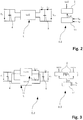
- FIG. 2 shows a simplified block diagram of a single LLC converter L and a corresponding control structure 6.2 comprising an output controller 11 and a pulse generator 2 for commanding the switches S1, S2, S3 and S4 (not explicitely shown in Figure 2 ) of the single LLC converter L.
- the LLC converter L uses the commonly known methods of output control, i.e. to control the output voltage V out or the output current I out .
- the output controller 11 compares the measured quantities of output voltage V out or output current I out with a desired set value and uses switching frequency (f s ) control and/or phase-shift ( ⁇ ) control to realize the set value by controlling the pulse generator 2 appropriately.
- the prior-art structure of interleaved LLC converters L is shown in Figure 3 for the case of two interleaved LLC converters L.
- the corresponding control structure 6.3 comprises one pulse generator 2 per single LLC converter L.
- the number of paralleled LLC converters L can be two or more with the appropriate phase-shift between the switching patterns of the two or more LLC converters L applied.
- the phase-shift between the switching patterns of both LLC converters L designated in the following as interleave phase-shift, should be around 90°, which must be realized by appropriate synchronization between the pulse generators 2 of each LLC converter L.
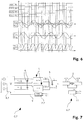
- Figure 4 shows switching patterns and waveforms in case of two interleaved LLC converters L with 90° interleave phase shift and an example mismatch between the circuit element values of both LLC converters L. Though the mismatch is not high in terms of what can be economically and practically reached, the load is very unbalanced between the LLC converters L as can be seen by the fact that A. i out ⁇ B. i out .
- FIG. 5 now shows a first embodiment of a converter arrangement C.5 according to the invention which has the objective to overcome the unbalanced loading at component value mismatch shown in Figure 4 .
- An active load balancing control 7.5 is added to the control structure 6.5. Its inputs are the measured output currents of the single converters (here: i out_A and i out_B ).
- the load balancing control 7.5 compares the single output currents to each other and takes action in order to balance the loading between the single LLC converters L by either applying more phase-shift (here: ⁇ A resp. ⁇ B ) to the single LLC converter L that is more loaded than the other or applying less phase-shift to the single LLC converter L that is less loaded than the other or by combining both actions.
- the load balancing control 7.5 would compare the single output currents to each other and would take action in order to balance the loading between the single LLC converters L by either applying more phase-shift (here: ⁇ A resp. ⁇ B ) to the single LLC converters L that are more loaded than the others or applying less phase-shift to the single LLC converters L that are less loaded than the others or by combining both actions.
- phase-shift here: ⁇ A resp. ⁇ B
- Figure 6 shows switching patterns and waveforms when the load balancing routine characteristic for the first embodiment as shown in Figure 5 is applied in case of the component value mismatch example used already in Figure 4 . It can be seen that a switching delay is applied between the diagonal switches S1 and S4 of the single LLC converter "LLC B". This switching delay or phase shift leads to a considerable load balancing as can be seen by looking at the currents A. i out and B. i out . at the bottom of Figure 6 .
- FIG. 7 shows a second embodiment of the invention.
- the converter arrangement shown here comprises a multi-link input source 8.7 and a control link 9 to this multi-link input source 8.7.
- the multi-link input source 8.7 is characterized by that it provides two DC voltage links and each of the links is connected to the input voltage of one single LLC converter L (here: V in_A and V in_B ). Furthermore, it is required that the input voltages supplied by the multi-link input source 8.7 can be adjusted within an appropriate range by using the control link 9.
- Examples for an applicable multi-link input source are the Vienna-rectifier in case of two interleaved single LLC converters L or multiple single (single phase and/or single rail) PFC rectifiers in case of an arbitrary number of interleaved single LLC converters L or a three-phase Y-rectifier facilitating three (or a multiple of three) independently adjustable input voltages for the single LLC converters L.
- Figure 7 the solution with a Vienna-rectifier connected to a three-phase alternating mains is shown.
- an active load balancing control 7.7 is added to the converter arrangement.
- the active load balancing control 7.5 shown in Figure 5 it is not shown as an integrated component of the control structure 6.7, but rather as an independent part of the converter arrangement. It is, however, also possible to integrate the active load balancing control 7.7 into the control structure 6.7.
- the inputs of the active load balancing control 7.7 are the measured output currents of the single LLC converters L (here: i out_A and i out_B ).
- the load balancing control 7.7 compares the single output currents to each other and takes action in order to balance the loading between the single LLC converters L by either decreasing the input voltage of the single LLC converter L that is more loaded than the other or by increasing the input voltage of the single LLC converter L that is less loaded than the other or by combining both actions.
- the load balancing control 7.7 would compare the single output currents to each other and would take action in order to balance the loading between the single LLC converters L by either decreasing the input voltages of the single LLC converters L that are more loaded than the others or by increasing the input voltages of the single LLC converters L that are less loaded than the others or by combining both actions.
- Figures 8 and 9 show a third and a fourth embodiment of the invention, respectively.
- a multi-link power source 8.8 comprising two single PFC rectifiers 10 is used.
- Each of the PFC rectifiers 10 supplies an input voltage to one single LLC converter L of the converter arrangement C.8.
- the embodiment shown in Figure 9 uses a three phase Y-rectifier to supply three input voltages to a converter arrangement C.9 comprising three single LLC converters L.
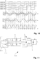
- Figure 10 shows switching patterns and waveforms when the load balancing routine characteristic for the second embodiment as shown in Figure 7 is applied in case of the component value mismatch example used already in Figure 4 .
- the application of this load balancing routine leads to a considerable load balancing visualized by the homogenized waveforms the currents A. i out and B. i out .
- FIG 11 shows a fifth embodiment of the invention.
- the converter arrangement C.11 comprises a multi-link input source 8.11 and a load balancing control 7.11.
- the load balancing control 7.11 is located within the multi-link input source 8.11, i. e. it is integrated in the multi-link input source 8.11.
- the load balancing control 7.11 has a power balancing configuration. By balancing the supply power to the two input voltage links, the output power of the two single LLC converters L are balanced as well. Because the output voltage is same for every single LLC converter, the several output currents are balanced as the output powers are balanced.
- FIG. 12 shows a sixth embodiment of the invention.
- the converter arrangement C.12 comprises two interleaved LLC converters LLC A and LLC B and two PFC-boost converters as source converters 8.12, one for each LLC converter. Both source converters 8.12 are connected in parallel to the same voltage source V src .
- the converter arrangement C.12 further comprises a load balancing control 7.12 which provides a control signal d A , d B to each source converter 8.12 such that the input currents i src_A and i src_B of the source converters 8.12 matches a reference current.
- the input power of a source converter is given by the product of the input voltage and the input current.
- the input power Pin srcx of each source converter is calculated by where V src is the input voltage, i srcx is the input current of converter number x and AC-Period designates the period of the AC line signal.
- the load balancing control 7.12 comprises a voltage controller 13 which receives the output voltages V in_A , V in_B of the source converters as input signals and generates a reference current i ref based on the output voltages V in_A , V in_B and a reference voltage (not shown) where the reference voltage is either generated internally or fed to the voltage controller 13.
- the reference current i ref is generated by comparing the output voltages V in_A , V in_B to the reference voltage and generating the reference current i ref based on a result of that comparison.
- the load balancing control 7.12 further comprises two current regulators 12.1, 12.2 which both receive the reference current i ref and one of the currents i src_A and i src_B respectively.
- the current regulators 12.1, 12.2 regulate the input currents i src_A and i src_B by measuring them, comparing them to the reference current i ref , generating a control signal d A , d B for each of the source converters 8.12 based on the result of this comparison and providing the control signals d A , d B to the respective source converters 8.12.
- the input currents i src_A and i src_B are identical (or at least similar) and both match the reference current i ref . And hence also the input powers of the source converters 8.12 are identical (or at least similar).
- the output power of the source converters 8.12 is fed to the power input of the respective LLC converter (L).
- the LLC output powers P out_A , P out_B are so as well since the current outputs are connected to a common output voltage bus, which can be seen from the following equations: where V out is the voltage of the output voltage bus.
- the input power of the LLC converters (L) will be unbalanced in accordance to the unbalanced output currents i out_A and i out_B . Because both source converters are feeding the DC links with the same power, the DC link voltage is going to increase for the LLC converter that draws less power than the other one and its going to decrease for the LLC converter that draws more power than the other one, thereby assuming that the overall input and output power of the converter arrangement are matched.
Landscapes
- Engineering & Computer Science (AREA)
- Power Engineering (AREA)
- Dc-Dc Converters (AREA)
- Ac-Ac Conversion (AREA)
Description
- The invention relates to a converter arrangement comprising at least two single LLC converters, one pulse generator per single LLC converter, wherein each pulse generator is configured to supply switching pulses to one single LLC converter, and an output controller configured to use switching frequency control and/or phase-shift control to control the pulse generators. In further, the invention relates to a method for operating said converter arrangements.
- LLC resonant converters are more and more used in modern power supply designs due to their ability to operate with high efficiency at moderate circuit and control complexity. Moreover, the interleaving method, i.e. combining multiple single LLC resonant converters, in particular in parallel connections, is commonly used in modern power supply designs to increase the maximum output power per unit, to spread power losses, to apply phase shedding in light load operation and to decrease the size of input and output filters. Additional measures such as active current sharing control are usually necessary for interleaved converters to balance the load among the single converters. Using the LLC converter in a parallel connection requires load balancing as well, especially if standard component value precision (e.g. ±5%) of the resonant circuit elements is given based on economical and practical matters. Unfortunately using common active current sharing methods known from interleaved PWM converters has some major drawbacks for resonant converters and/or LLC converters in parallel connection: The switching frequencies of the paralleled converters would be close to each other but not perfectly the same, resulting in beat frequency effects that can be very critical to EMI requirements and thus afford extensive filtering. Also the desired current ripple cancellation effect of interleaved switching converters would not be in effect making again bigger filters necessary. Motivated by those issues, several workarounds to realize load balancing for interleaved LLC converters have been proposed (for example in
US 20090231887 ), but these methods all have the disadvantage of reducing the reliability and practicability of the resulting LLC converter arrangement compared to the performance of the original LLC converter.US2012153730 discloses an interleaved LLC power converter wherein each LLC converter comprises its own source converter. Both source converters are connected to the same voltage source. In order to compensate for the tolerances the converter includes a compensation controller, which adjusts the input currents of the LLC converters. - It is the object of the invention to create a converter arrangement pertaining to the technical field initially mentioned, that is able to overcome unbalanced loading of its different single LLC converters while maintaining a good reliability, practicability and efficiency of the converter arrangement.
- The present invention is defined in the appendent independent claims.
- In an example, the converter arrangement comprises an input capacitor and an output capacitor. The load balancing control is preferably an active load balancing control.
- Such a converter arrangement has the advantage that unbalanced loading of the different single LLC converters can be overcome in a reliable and convenient manner.
- Power supply of the LLC converters can be done in various ways. For example by connecting them directly to an external power source such as an AC or DC line or by providing an externally fed power source and connecting each LLC converter to that power source.
- The source converter is for example a power source converter such as a PFC boost converter. Each source converter is connected to an input of exactly one LLC converter to supply power, e. g. a supply voltage, to that LLC converter. Each source converter is configured to be fed by a common power source. This power source may either be a DC power source, an AC power source or an AC/DC combined power source. The source converters are preferably configured to receive a voltage at their input which means that the common power source preferably is a voltage source. In order to balance the load of the LLC converters, the load balancing control is configured to balance an input power of the source converters.
- Input power balancing of the source converters generally may be achieved by controlling the input voltage, the input current or both. Since each source converter is connected to the same voltage source, the input voltage is identical for each source converter. Their input power will therefore be identical if also their input currents are identical. According to the law of energy conservation, the output power of the source converters is identical or at least similar if their input power is identical or at least similar (provided that the conversion efficiency of the source converters is identical or at least similar).
- The reference current is the same for each current regulator or in other words, it is a common reference current.
- An advantage of this load balancing is that it requires the generation of just one single reference current, which results in a simple design and low production costs. Moreover, requirement of exactly one single reference current is inherent to the functional principle of this balancing control. Or in other words, this balancing control will not work with more then one reference current, because the output power of the source converters can only be balanced if it is ensured that - with identical input voltages - their input currents are identical. But having different reference currents and therewith different input currents of the source converters will not result in the same output power. The common reference current therefore is a key functionality of this embodiment to achieve balanced LLC output currents.
- The reference current may be provided by an external current source. But in order to balance the LLC loads, the converter arrangement preferably comprises a voltage controller for generating the reference current. This single voltage controller thereby generates the reference current based on the output voltage of at least one of the source converters. Preferably, the output voltage of every single source converter is considered for generating the reference current. Reference current generation is preferably done by performing a comparison of the single or the multiple source converter output voltages to a suitable reference voltage and then generating the reference current based on a result of that comparison.
- The above mentioned input capacitor is a part of the so called DC link capacitance which is understood as the capacitance formed by all capacitances that are connected to the respective DC link bus voltage feeding an LLC converter. This DC link capacitance performs as a power buffer when feeding the power output of a source converter to the input of the respective LLC converter. In case the output powers of the source converter and the respective LLC converter are unmatched, the power difference is fed to or drawn from the DC link capacitance, thereby increasing or decreasing the respective DC link voltage. Therefore, in case the LLC output currents are unbalanced, the LLC output powers are so as well since the current outputs are connected to a common output voltage bus. Due to the law of energy conservation the input power of the LLC converters is unbalanced too, i. e. in accordance with the unbalanced output power (provided that the conversion efficiency of the LLC converters is identical or at least similar). Because the source converters are feeding the DC links with the same power, the DC link voltage is going to increase for those LLC converters that draw less power than the others and its going to decrease for those LLC converters that draw more power than the others (assuming that the overall input and output power of the converter arrangement are matched). The speed of this dynamic process is given by the amount of power mismatch between the LLC converters, the DC link voltage level and the DC link capacitance. The process will continue until a steady state is reached in which the LLC converters draw equal or at least similar input power and supply equal or at least similar output power to the output voltage bus, thereby feeding matched output currents with equal or at least similar average values.
- In the following, other preferred embodiments of converter arrangements with interleaved LLC converters and a load balancing control are described.
- In a preferred embodiment of the invention, the load balancing control comprises one input per single LLC converter. This has the advantage that from each single LLC converter, information can be separately and individually be supplied to the load balancing control. In a particularly preferred embodiment, the load balancing control comprises exactly one input per single LLC converter. This has the advantage that the number of ports and/or wirings in the converter arrangement is minimized and that the converter arrangement is therefore comparably simple. However, the balancing control can also comprise more than one input per single LLC converter, for example electrical variables measured at different points of each single LLC converter, or even less than one input per single LLC converter, for example one input for two or three LLC converters taken together.
- In a preferred embodiment, the load balancing control comprises one output per single LLC converter. This has the advantage that each single LLC converter can be separately controlled in respect of its balancing. This has the advantage that the number of ports and/or wirings in the converter arrangement is minimized and that the converter arrangement is therefore comparably simple. However, the balancing control can also comprise more than one output per single LLC converter, for example different electrical variables for influencing the behavior of each single LLC converter at different locations, or even less than one output per single LLC converter, for example one output for two or three LLC converters taken together.
- In an example, the load balancing control is configured to use output currents of the single LLC converters as input variables. This is advantageous because the output currents are ideal for determining a load mismatch of the converter arrangement, for example to the range of their amplitudes and their phase shifts. However, it is also possible that the load balancing control uses other information of the single LLC converters like other currents and/or voltages (such as currents and/or voltages measured at different points inside each single LLC converter), as input variables.
- In an example, the load balancing control is configured to determine a specific phase information for each pulse generator and preferably also to supply this specific phase information to each pulse generator. Such a phase information has the advantage that it can for example be used to introduce a phase shift into the switching of two of the four switches of each single LLC converter, preferably into the switching of two diagonal switches of each single LLC converter. The load balancing control can, however also be configured to supply other types of information to the pulse generators or yet to other components of the converter arrangement.
- In an example, the load balancing control is configured to compare the output currents of the single LLC converters to each other. This has the advantage that a corresponding action of the load balancing control can be based on the comparison of the behaviour of all single LLC converters. However, it is also possible that the load balancing control is configured to compare other variables related to the behaviour of the converter arrangement and/or the single LLC converters, like currents or voltages tapped at other locations inside the converter arrangement, to each other.
- In an example, the load balancing control is configured to balance a loading between the single LLC converters by applying more phase-shift to a single LLC converter that is more loaded than another single LLC converter and/or applying less phase-shift to a single LLC converter that is less loaded than another single LLC converter. It is particularly advantageous if the more and/or less phase shift is applied to at least two, preferably diagonal, switches of the single LLC converters, preferably of each single LLC converter. Introducing a phase shift to at least certain pairs of switches in the LLC converters leads to a comparably simple and yet reliable way of balancing the loads of the converter arrangement according to the invention. However, phase shifting configurations other than the one explained above are, in principle, also possible. In a more general phase shifting configuration, the phase shift is introduced between the turn-off switching events of at least two, preferably diagonal, switches of the single LLC converters. The turn-on switching events of every switch may be delayed in any appropriate manner. In an example, the load balancing control is configured to carry out the described phase shifting modulation in such a way that a resonant-current-depending, adaptive delay of the turn-on edges of the switches, which can for example be field effect transistors, is used.
- In an example, the converter arrangement comprises a multi-link input source comprising one DC voltage link per single LLC converter. Each DC voltage link of the multi-link input source is preferably connected to the input voltage of one single LLC converter. The use of such a multi-link input source has the advantage that the DC input voltage for each single LLC converter can be determined separately by the balancing control and the load mismatch can thereby be corrected through application of appropriate DC input voltages to the concerned single LLC converters. However, it is also possible to use a multi-link input source that supplies multiple DC voltage links wherein each voltage serves as an input to at two or more single LLC converters.
- In an example, the multi-link input source comprises a Vienna-rectifier (typically a unidirectional three-phase, three-switch, three-level rectifier using pulse-width modulation (PWM)) and/or multiple single (single phase and/or single rail) PFC rectifiers (rectifiers using power factor correction (PFC)), preferably one single PFC rectifier per single LLC converter, and/or a three-phase Y-rectifier (typically formed by a star connection of three single-phase unity power factor rectifier systems). However it is also possible to use different types of input sources as long as they are able to supply at least two different DC voltage links, preferably one single DC voltage link per single LLC converter.
- In an example, the load balancing control is configured to determine a specific voltage information for each DC voltage link of the multi-link input source, preferably as a function of the input to the balancing control from the different single LLC converters. This has the advantage that quick and straightforward reaction to a load mismatch of the converter arrangement is obtained due to the translation of the output current of each single LLC converter into a corresponding DC input voltage for each single LLC converter. It is however also possible for the load balancing control to determine another information than a voltage information to the multi-link input source, for example merely a boolean value for each single LLC converter which is true when the corresponding voltage needs to be increased and false when it needs to be decreased.
- In an example, the load balancing control and/or the multi-link input source are/is configured to balance a loading between the single LLC converters by decreasing an input voltage of a single LLC converter that is more loaded than another single LLC converter and/or increasing an input voltage of a single LLC converter that is less loaded than another single LLC converter. Preferably, the input voltage(s) is/are decreased and/or increased by adapting the specific voltage information supplied by the balancing control to the multi-link input source for each DC voltage link. Such a configuration of the load balancing control and/or the multi-link input source is advantageous because it is particularly easy to implement in the balancing control (e. g. as a PI controller) and because it leads to a good load mismatch correction / load balancing at the same time. Other configurations of the load balancing control and/or the multi-link input source are, however, also possible as long as the overall goal - i. e. to obtain a good load balancing - is obtained through appropriate control of the multi-link input source.
- In an example, the load balancing control is integrated in the multi-link input source. However, the load balancing control can also only be connected to the multi-link input source in such a way that the load balancing control and the multi-link input source form a logical entity, for example through appropriate connections. A physical integration of the components is not absolutely necessary.
- In an example, the load balancing control is configured to balance a loading between the single LLC converters by balancing supply powers to the several voltage links of the multi-link input source. This has the advantage to allow a comparably simple load balancing.
- The use of such a load balancing routine has the advantage that load mismatch and/or unstable and/or inefficient operation of the converter arrangement can be avoided.
- In an example, each single LLC converter comprises four switches.
- In an example, each LLC converter is supplied with a supply voltage by exactly one source converter, particularly a PFC boost converter. Performing the load balancing routine then comprises the step of balancing an input power of the source converters.
- In another preferred embodiment, the reference current is generated based on an output voltage of the source converters, in particular by performing a comparison of the output voltage of the at least one source converter and a reference voltage and generating the reference current based on a result of that comparison.
- In an example, the load balancing routine uses one variable per single LLC converter, preferably an output current of the single LLC converter, as input variables and/or the load balancing routine supplies one output information per single LLC converter. The advantage of a balancing routine functioning in this way is that it is possible for the balancing routine to take into account the performance for each single LLC converter and to influence the performance of each single LLC converter separately. However, it is also possible that the load balancing routine uses other variables such as voltages and/or input and/or outputs only for selected single LLC converters and/or for groups of single LLC converters.
- In an example the load balancing routine determines a specific phase information for each pulse generator, preferably by comparing the output currents of the single LLC converters to each other. Preferably, the load balancing routine then supplies this specific phase information to each pulse generator. This has the advantage that each pulse generator is able to react to the loading of its respective single LLC converter separately, which leads to a particularly precise load balancing. However, other configurations of the load balancing routine, e. g. the use of common phase in formations for groups of single LLC converters are in principle also possible.
- In an example, the load balancing routine balances a loading between the single LLC converters by applying more phase-shift to a single LLC converter that is more loaded than another single LLC converter and/or by applying less phase-shift to a single LLC converter that is less loaded than another single LLC converter. It is particularly preferred if the load balancing routine applies more phase-shift to a pair of preferably diagonal switches, e. g. MOSFETs, of a single LLC converter that is more loaded than another single LLC converter and/or by applying less phase-shift to a pair of preferably diagonal switches, e. g. MOSFETs, of a single LLC converter that is less loaded than another single LLC converter.
- In an example, the load balancing routine balances a loading between the single LLC converters by determining a specific voltage information for each single LLC converter and preferably by supplying this specific voltage information to a multi-link input source which supplies a distinct input voltage according to the specific voltage information to every single LLC converter.
- In an example, an interleave phase-shift between the single LLC converters is readjusted dynamically. This has, for example, the advantage of sustaining best current ripple cancellations of input and output currents.
- In an example, the load balancing routine balances a loading between the single LLC converters by determining a specific power information for each single LLC converter and/or a specific power information for a voltage link of each single LLC converter. This leads to a simple way of load balancing: since the output voltage is the same for every single LLC converter, the output currents are balanced if the input and/or output powers are balanced.
- Other advantageous embodiments and combinations of features come out from the detailed description below and the totality of the claims.
- The drawings used to explain the embodiments show:
- Fig. 1:
- Commonly known LLC converter basic structure,
- Fig. 2:
- Simplified block diagram of basic control structure applied to a single LLC converter,
- Fig. 3:
- Simplified block diagram of prior-art control structure for interleaved LLC converters,
- Fig. 4:
- Switching patterns and waveforms for interleaved LLC converters with no balancing measures applied,
- Fig. 5:
- Simplified block diagram of a first embodiment of the invention: proposed control structure for interleaved LLC converters including load balancing control,
- Fig. 6:
- Switching patterns and waveforms for interleaved LLC converters with balancing routine of an example,
- Fig. 7:
- Simplified block diagram of a second embodiment of the invention: proposed control structure for interleaved LLC converters including load balancing control,
- Fig. 8
- Simplified block diagram of a third embodiment of the invention: proposed control structure for interleaved LLC converters including load balancing control,
- Fig. 9
- Simplified block diagram of a fourth embodiment of the invention: proposed control structure for interleaved LLC converters including load balancing control,
- Fig. 10:
- Switching patterns and waveforms for interleaved LLC converters with balancing routine according to second embodiment of invention applied, and
- Fig. 11:
- Simplified block diagram of a fifth embodiment of the invention: proposed control structure for interleaved LLC converters including load balancing control.
- Fig. 12:
- Simplified block diagram of a sixth embodiment of the invention: proposed control structure for interleaved LLC converters including load balancing control.
- Fig. 13:
- Simplified block diagram of the load balancing control of the sixth embodiment of the invention.
- In the figures, the same components are given the same reference symbols.
- The invention is based on the commonly known structure of the LLC converter L as shown in
Figure 1 . The LLC converter L comprises aresonant circuit 1, an inverter comprising four switches S1, S2, S3 and S4 and arectifier 3. The LLC converter L is combined with aninput capacitance 4 and anoutput capacitance 5. The rectifier can be of full-wave or center-tapped type, realized by diodes or by MOSFETs for the purpose of synchronous rectification. The arrangement order of theresonant circuit 1 elements Ls,Lp||X,Cs is arbitrary, they could as well be divided into several sub-elements that sum to the original value. The inverter is shown as full-bridge type; this configuration is necessary for the embodiment and method of the invention visualized inFigures 5 and6 . However, in certain cases such as the embodiment and method of the invention visualized inFigures 7 ,8 ,9 and10 the inverter may either be of full-bridge type or of half-bridge type. -
Figure 2 shows a simplified block diagram of a single LLC converter L and a corresponding control structure 6.2 comprising anoutput controller 11 and apulse generator 2 for commanding the switches S1, S2, S3 and S4 (not explicitely shown inFigure 2 ) of the single LLC converter L. In this setup, the LLC converter L uses the commonly known methods of output control, i.e. to control the output voltage Vout or the output current Iout. Theoutput controller 11 compares the measured quantities of output voltage Vout or output current Iout with a desired set value and uses switching frequency (fs) control and/or phase-shift (ϕ) control to realize the set value by controlling thepulse generator 2 appropriately. - Based on the single LLC structure shown in
Figure 2 , the prior-art structure of interleaved LLC converters L is shown inFigure 3 for the case of two interleaved LLC converters L. The corresponding control structure 6.3 comprises onepulse generator 2 per single LLC converter L. The number of paralleled LLC converters L can be two or more with the appropriate phase-shift between the switching patterns of the two or more LLC converters L applied. In case of two converters, the phase-shift between the switching patterns of both LLC converters L, designated in the following as interleave phase-shift, should be around 90°, which must be realized by appropriate synchronization between thepulse generators 2 of each LLC converter L. -
Figure 4 shows switching patterns and waveforms in case of two interleaved LLC converters L with 90° interleave phase shift and an example mismatch between the circuit element values of both LLC converters L. Though the mismatch is not high in terms of what can be economically and practically reached, the load is very unbalanced between the LLC converters L as can be seen by the fact that A.i out << B.i out. -
Figure 5 now shows a first embodiment of a converter arrangement C.5 according to the invention which has the objective to overcome the unbalanced loading at component value mismatch shown inFigure 4 . An active load balancing control 7.5 is added to the control structure 6.5. Its inputs are the measured output currents of the single converters (here: i out_A and i out_B). The load balancing control 7.5 compares the single output currents to each other and takes action in order to balance the loading between the single LLC converters L by either applying more phase-shift (here: ϕA resp. ϕB) to the single LLC converter L that is more loaded than the other or applying less phase-shift to the single LLC converter L that is less loaded than the other or by combining both actions. "Applying more phase-shift to the converter" is to be understood as "increasing a switching delay between the switches S1 and S4 (or the switches S2 and S3), at least between the turn-off switching events of the switches S1 and S4 (or S2 and S3) of the respective single LLC converter L" whereas "applying less phase-shift" is to be understood as "decreasing the switching delay between the switches S1 and S4 (or the switches S2 and S3), at least between the turn-off switching events of the switches S1 and S4 (or S2 and S3) of the respective single LLC converter L". In a converter arrangement with more than two single LLC converters L (this case is not shown inFigure 5 ), the load balancing control 7.5 would compare the single output currents to each other and would take action in order to balance the loading between the single LLC converters L by either applying more phase-shift (here: ϕA resp. ϕB) to the single LLC converters L that are more loaded than the others or applying less phase-shift to the single LLC converters L that are less loaded than the others or by combining both actions. When altering the phase-shifts applied to the single LLC converters L, it may be convenient to readjust the interleave phase-shift in order to sustain e.g. best current ripple cancellation of input and output currents. -
Figure 6 shows switching patterns and waveforms when the load balancing routine characteristic for the first embodiment as shown inFigure 5 is applied in case of the component value mismatch example used already inFigure 4 . It can be seen that a switching delay is applied between the diagonal switches S1 and S4 of the single LLC converter "LLC B". This switching delay or phase shift leads to a considerable load balancing as can be seen by looking at the currents A.i out and B.i out. at the bottom ofFigure 6 . -
Figure 7 shows a second embodiment of the invention. The converter arrangement shown here comprises a multi-link input source 8.7 and acontrol link 9 to this multi-link input source 8.7. The multi-link input source 8.7 is characterized by that it provides two DC voltage links and each of the links is connected to the input voltage of one single LLC converter L (here: V in_A and V in_B). Furthermore, it is required that the input voltages supplied by the multi-link input source 8.7 can be adjusted within an appropriate range by using thecontrol link 9. Examples for an applicable multi-link input source are the Vienna-rectifier in case of two interleaved single LLC converters L or multiple single (single phase and/or single rail) PFC rectifiers in case of an arbitrary number of interleaved single LLC converters L or a three-phase Y-rectifier facilitating three (or a multiple of three) independently adjustable input voltages for the single LLC converters L. InFigure 7 , the solution with a Vienna-rectifier connected to a three-phase alternating mains is shown. As in the embodiment shown inFigure 5 , an active load balancing control 7.7 is added to the converter arrangement. However, in contrast to the active load balancing control 7.5 shown inFigure 5 , it is not shown as an integrated component of the control structure 6.7, but rather as an independent part of the converter arrangement. It is, however, also possible to integrate the active load balancing control 7.7 into the control structure 6.7. The inputs of the active load balancing control 7.7 are the measured output currents of the single LLC converters L (here: i out_A and i out_B). The load balancing control 7.7 compares the single output currents to each other and takes action in order to balance the loading between the single LLC converters L by either decreasing the input voltage of the single LLC converter L that is more loaded than the other or by increasing the input voltage of the single LLC converter L that is less loaded than the other or by combining both actions. In a converter arrangement with more than two single LLC converters L (this case is not shown inFigure 7 ), the load balancing control 7.7 would compare the single output currents to each other and would take action in order to balance the loading between the single LLC converters L by either decreasing the input voltages of the single LLC converters L that are more loaded than the others or by increasing the input voltages of the single LLC converters L that are less loaded than the others or by combining both actions. -
Figures 8 and 9 show a third and a fourth embodiment of the invention, respectively. InFigure 8 , a multi-link power source 8.8 comprising twosingle PFC rectifiers 10 is used. Each of thePFC rectifiers 10 supplies an input voltage to one single LLC converter L of the converter arrangement C.8. The embodiment shown inFigure 9 uses a three phase Y-rectifier to supply three input voltages to a converter arrangement C.9 comprising three single LLC converters L. -
Figure 10 shows switching patterns and waveforms when the load balancing routine characteristic for the second embodiment as shown inFigure 7 is applied in case of the component value mismatch example used already inFigure 4 . As can be seen at the bottom ofFigure 10 , the application of this load balancing routine leads to a considerable load balancing visualized by the homogenized waveforms the currents A.i out and B.i out. -
Figure 11 shows a fifth embodiment of the invention. The converter arrangement C.11 comprises a multi-link input source 8.11 and a load balancing control 7.11. The load balancing control 7.11 is located within the multi-link input source 8.11, i. e. it is integrated in the multi-link input source 8.11. The load balancing control 7.11 has a power balancing configuration. By balancing the supply power to the two input voltage links, the output power of the two single LLC converters L are balanced as well. Because the output voltage is same for every single LLC converter, the several output currents are balanced as the output powers are balanced. -
Figure 12 shows a sixth embodiment of the invention. The converter arrangement C.12 comprises two interleaved LLC converters LLC A and LLC B and two PFC-boost converters as source converters 8.12, one for each LLC converter. Both source converters 8.12 are connected in parallel to the same voltage source Vsrc. The converter arrangement C.12 further comprises a load balancing control 7.12 which provides a control signal dA, dB to each source converter 8.12 such that the input currents isrc_A and isrc_B of the source converters 8.12 matches a reference current. - Generally, the input power of a source converter is given by the product of the input voltage and the input current. In case of PFC-boost converters that are connected to an AC line, the input power Pinsrcx of each source converter is calculated by

- The load balancing control 7.12 comprises a
voltage controller 13 which receives the output voltages Vin_A, Vin_B of the source converters as input signals and generates a reference current iref based on the output voltages Vin_A, Vin_B and a reference voltage (not shown) where the reference voltage is either generated internally or fed to thevoltage controller 13. The reference current iref is generated by comparing the output voltages Vin_A, Vin_B to the reference voltage and generating the reference current iref based on a result of that comparison. The load balancing control 7.12 further comprises two current regulators 12.1, 12.2 which both receive the reference current iref and one of the currents isrc_A and isrc_B respectively. The current regulators 12.1, 12.2 regulate the input currents isrc_A and isrc_B by measuring them, comparing them to the reference current iref, generating a control signal dA, dB for each of the source converters 8.12 based on the result of this comparison and providing the control signals dA, dB to the respective source converters 8.12. - If the current regulators 12.1, 12.2 are working sufficiently in terms of speed and accuracy, the input currents isrc_A and isrc_B are identical (or at least similar) and both match the reference current iref. And hence also the input powers of the source converters 8.12 are identical (or at least similar).
- The output power of the source converters 8.12 is fed to the power input of the respective LLC converter (L). The DC link capacitance of each DC link from a source converter 8.12 to the corresponding LLC converter (L), which includes the
input capacitance 4 as well as every other capacitance connected to that DC link, thereby performs as a power buffer. In case the output currents iout_A and iout_B of the LLC converters (L) are unbalanced, the LLC output powers Pout_A, Pout_B are so as well since the current outputs are connected to a common output voltage bus, which can be seen from the following equations:
Claims (12)
- Converter arrangement (C.5, C.8, C.11, C.12), comprisinga) at least two single LLC converters (L),b) a pulse generator (2) per single LLC converter (L), wherein each pulse generator (2) is configured to supply switching pulses to one single LLC converter (L) andc) an output controller (11) configured to use switching frequency control and/or phase-shift control to control the pulse generators (2),d) a load balancing control (7.8, 7.11, 7.12) for controlling load balancing of the converter arrangement (C.5, C.8, C.11, C.12),e) a source converter (8.12) per LLC converter (L), wherein each source converter (8.12) is connected to an input of exactly one LLC converter (L) to supply a supply voltage (Vin_A, Vin_B) to that LLC converter (L), wherein each source converter (8.12) is configured to be fed by a common power source,f) the load balancing control (7.8, 7.11, 7.12) is configured to balance an input power of the source converters (8.12)
characterized in thatg) the load balancing control (7.8, 7.11, 7.12) comprises a current regulator (12.1, 12.2) per source converter (8.12) configured to balance an input current (isrc_A, isrc_B) of the source converters (8.12) by comparing each input current (isrc_A, isrc_B) to a common reference current (iref) and matching the input currents (isrc_A, isrc_B) to the common reference current (iref). - Converter arrangement (C.5, C.8, C.11, C.12) according to claim 1, characterized in that the load balancing control (7.8, 7.11, 7.12) comprises a voltage controller (13) for generating the reference current (iref) based on an output voltage of at least one of the source converters (8.12), preferably by performing a comparison of the output voltage of the at least one source converter and a reference voltage and generating the reference current based on a result of that comparison.
- Converter arrangement (C.5, C.8, C.11, C.12) according to any of the previous claims, characterized in that the load balancing control (7.8, 7.11, 7.12) comprises one input per single LLC converter (L).
- Converter arrangement (C.5, C.8, C.11, C. 12) according to claim 3, characterized in that the load balancing control (7.8, 7.11, 7.12) comprises one output per single LLC converter (L).
- Method for operating a converter arrangement (C.5, C.8, C.11, C.12), comprising at least two single LLC converters (L), a pulse generator (2) per single LLC converter (L) and a control unit, whereina) each pulse generator (2) supplies switching pulses to one single LLC converter (L) andb) switching frequency control and/or phase-shift control is used to control the pulse generators (2),c) the control unit performs a load balancing routine for controlling load balancing of the converter arrangement (C.5, C.8, C.11, C.12),d) each LLC converter (L) is supplied with a supply voltage (Vin_A, Vin_B) by exactly one source converter (8.12),e) performing the load balancing routine comprises balancing an input power of the source converters (8.12) which are supplied from a common power source characterized in thatf) balancing the input power of the source converters comprises balancing an input current (isrc_A, isrc_B) of each source converter (8.12) by comparing the input current (isrc_A, isrc_B) to a common reference current (iref) and matching the input currents (isrc_A, isrc_B) to the common reference current (iref).
- Method according to claim 5, characterized in that the reference current (iref) is generated based on an output voltage of the source converters (8.12), particularly by performing a comparison of the output voltage of the at least one source converter and a reference voltage and generating the reference current based on a result of that comparison.
- Converter arrangement (C.5, C.8, C.11, C.12) according to any of claims 3 or 4, characterized in that it comprises a multi-link input source (8.8, 8.11) comprising one DC voltage link per single LLC converter (L).
- Converter arrangement (C.5, C.8, C.11, C.12) according to claim 7, characterized in that the multi-link input source (8.8, 8.11) comprises multiple single PFC rectifiers.
- Converter arrangement (C.5, C.8, C.11, C.12) according to any of claims 7 or 8, characterized in that the load balancing control (7.8, 7.11, 7.12) is configured to determine a specific voltage information for each DC voltage link of the multi-link input source (8.8, 8.11).
- Converter arrangement (C.5, C.8, C.11, C.12) according to any of claims 7 to 9, characterized in that the load balancing control (7.8, 7.11, 7.12) is configured to balance a loading between the single LLC converters (L) by decreasing an input voltage of a single LLC converter (L) that is more loaded than another single LLC converter (L) and/or increasing an input voltage of a single LLC converter (L) that is less loaded than another single LLC converter (L).
- Converter arrangement (C.5, C.8, C.11, C.12) according to any of the claims 7 to 10, characterized in that the load balancing control (7.8, 7.11, 7.12) is integrated in the multi-link input source (8.8, 8.11).
- Converter arrangement (C.5, C.8, C.11, C.12) according to any of claims 7 to 11, characterized in that the load balancing control (7.8, 7.11, 7.12) is configured to balance a loading between the single LLC converters (L) by balancing supply powers to the several voltage links of the multi-link input source (8.8, 8.11).
Applications Claiming Priority (2)
| Application Number | Priority Date | Filing Date | Title |
|---|---|---|---|
| EP12405061.8A EP2683066B1 (en) | 2012-07-04 | 2012-07-04 | LLC balancing |
| EP13405079.8A EP2683067B1 (en) | 2012-07-04 | 2013-07-03 | LLC Balancing |
Related Parent Applications (3)
| Application Number | Title | Priority Date | Filing Date |
|---|---|---|---|
| EP13405079.8A Division EP2683067B1 (en) | 2012-07-04 | 2013-07-03 | LLC Balancing |
| EP13405079.8A Previously-Filed-Application EP2683067B1 (en) | 2012-07-04 | 2013-07-03 | LLC Balancing |
| EP13405079.8A Division-Into EP2683067B1 (en) | 2012-07-04 | 2013-07-03 | LLC Balancing |
Publications (2)
| Publication Number | Publication Date |
|---|---|
| EP3416274A1 EP3416274A1 (en) | 2018-12-19 |
| EP3416274B1 true EP3416274B1 (en) | 2021-09-15 |
Family
ID=48747496
Family Applications (3)
| Application Number | Title | Priority Date | Filing Date |
|---|---|---|---|
| EP12405061.8A Active EP2683066B1 (en) | 2012-07-04 | 2012-07-04 | LLC balancing |
| EP13405079.8A Active EP2683067B1 (en) | 2012-07-04 | 2013-07-03 | LLC Balancing |
| EP18179920.6A Active EP3416274B1 (en) | 2012-07-04 | 2013-07-03 | Llc balancing |
Family Applications Before (2)
| Application Number | Title | Priority Date | Filing Date |
|---|---|---|---|
| EP12405061.8A Active EP2683066B1 (en) | 2012-07-04 | 2012-07-04 | LLC balancing |
| EP13405079.8A Active EP2683067B1 (en) | 2012-07-04 | 2013-07-03 | LLC Balancing |
Country Status (5)
| Country | Link |
|---|---|
| US (3) | US9263951B2 (en) |
| EP (3) | EP2683066B1 (en) |
| CN (3) | CN108521225B (en) |
| HK (1) | HK1258777A1 (en) |
| TW (1) | TWI514711B (en) |
Families Citing this family (30)
| Publication number | Priority date | Publication date | Assignee | Title |
|---|---|---|---|---|
| EP2683066B1 (en) * | 2012-07-04 | 2017-05-03 | DET International Holding Limited | LLC balancing |
| CN104348342B (en) * | 2013-08-02 | 2019-05-31 | 通用电气公司 | Electric energy conversion system and method |
| JP2015139258A (en) | 2014-01-21 | 2015-07-30 | サンケン電気株式会社 | Switching power supply device |
| US9356521B2 (en) | 2014-01-30 | 2016-05-31 | Sanken Electric Co., Ltd. | Switching power-supply device having wide input voltage range |
| US9356519B2 (en) * | 2014-02-12 | 2016-05-31 | Sanken Electric Co., Ltd. | Current balance circuit of resonant type switching power-supply circuit |
| US9746502B2 (en) * | 2014-11-03 | 2017-08-29 | General Electric Company | Systems and methods for monitoring and controlling a power converter |
| DE102015006210A1 (en) | 2015-05-13 | 2016-11-17 | Finepower Gmbh | Method for operating at least two electrically interconnected inverter |
| EP3176901A1 (en) * | 2015-12-01 | 2017-06-07 | DET International Holding Limited | Controller for a multiphase inverter |
| KR101856008B1 (en) | 2016-06-30 | 2018-05-10 | 한국에너지기술연구원 | Interleaved llc resonant converter and control method thereof |
| CN106953521B (en) * | 2016-09-08 | 2019-06-07 | 湘潭大学 | A kind of H bridge bi-directional DC-DC modulation strategy based on dual carrier modulation |
| TWI603572B (en) * | 2016-10-19 | 2017-10-21 | Fu-Tzu Hsu | Resonance damper |
| CN108155818A (en) * | 2016-12-05 | 2018-06-12 | 沃尔缇夫能源系统公司 | A kind of multiphase controlled resonant converter and its current equalizing method |
| JP6531751B2 (en) * | 2016-12-13 | 2019-06-19 | トヨタ自動車株式会社 | Power system |
| US20180191168A1 (en) * | 2017-01-04 | 2018-07-05 | National Instruments Corporation | Parallel Interleaved Multiphase LLC Current Sharing Control |
| WO2018190249A1 (en) * | 2017-04-12 | 2018-10-18 | 国立大学法人京都大学 | Switching power supply system, controller, and control method |
| EP3401935B1 (en) | 2017-05-08 | 2020-12-02 | Delta Electronics (Thailand) Public Co., Ltd. | Integrated magnetic component and power converter |
| CN107612335B (en) * | 2017-09-20 | 2019-10-25 | 武汉南华工业设备工程股份有限公司 | An Interleaved Parallel Control Method for Three-level LLC Resonant Converters |
| CN107834816A (en) * | 2017-11-07 | 2018-03-23 | 深圳威迈斯电源有限公司 | Two-stage multi-channel parallel flow equalizing circuit, current equalizing method, storage device and mobile terminal |
| US20190181744A1 (en) * | 2017-12-11 | 2019-06-13 | Texas Instruments Incorporated | Bus converter current ripple reduction |
| JP6673948B2 (en) * | 2018-01-29 | 2020-04-01 | ファナック株式会社 | Power control device and control method of power control device |
| CN110971135B (en) * | 2018-09-29 | 2021-07-13 | 中车株洲电力机车研究所有限公司 | Three-level full-bridge direct-current converter and control method thereof |
| EP3772170A1 (en) | 2019-07-30 | 2021-02-03 | Delta Electronics (Thailand) Public Co., Ltd. | Llc converter having a plurality of inverters |
| DE102019212887A1 (en) * | 2019-08-28 | 2021-03-04 | Robert Bosch Gmbh | Control method for a DC voltage converter and DC voltage converter |
| EP4560909A3 (en) | 2020-09-04 | 2025-08-20 | Delta Electronics (Thailand) Public Co., Ltd. | Power balancing in interleaved llc converters via duty cycle variation |
| CN112636617B (en) * | 2020-10-30 | 2022-07-15 | 平高集团储能科技有限公司 | Control method of Vienna rectifier |
| US11929671B2 (en) * | 2021-04-27 | 2024-03-12 | Semiconductor Components Industries, Llc | Current-mode control for multistage interleaved resonant converters |
| TWI784867B (en) | 2022-01-13 | 2022-11-21 | 宏碁股份有限公司 | Full-bridge resonant converter capable of suppressing high-frequency decoupling distortion |
| US12261537B2 (en) * | 2022-07-11 | 2025-03-25 | Texas Instruments Incorporated | Interleaved phase current balancing |
| KR102741910B1 (en) * | 2022-12-27 | 2024-12-16 | 한국전자기술연구원 | Power imbalance prevention circuit and method of resonance type power converter |
| CN121710709A (en) * | 2024-09-20 | 2026-03-20 | 维谛公司 | Current sharing control method and AC-DC conversion system |
Family Cites Families (23)
| Publication number | Priority date | Publication date | Assignee | Title |
|---|---|---|---|---|
| SU671012A1 (en) * | 1978-02-02 | 1979-06-30 | Московский Ордена Ленина Энергетический Институт | Multi-rotor electric drive compensator |
| JPH01234086A (en) * | 1988-03-15 | 1989-09-19 | Kobe Steel Ltd | Upper/lower roll load balancing method for rolling mill |
| JP3307814B2 (en) * | 1995-12-15 | 2002-07-24 | 株式会社日立製作所 | DC power supply |
| US6778415B2 (en) | 2003-01-22 | 2004-08-17 | O2Micro, Inc. | Controller electrical power circuit supplying energy to a display device |
| US7035125B2 (en) * | 2003-02-05 | 2006-04-25 | Matsushita Electric Industrial Co., Ltd. | Switching power supply and control method for the same |
| US20040160216A1 (en) * | 2003-02-06 | 2004-08-19 | Proton Energy Systems, Inc. | Method and system for configuring power electronics in an electrochemical cell system |
| US8618788B2 (en) * | 2007-03-30 | 2013-12-31 | Malay Trivedi | Dynamically adjusted multi-phase regulator |
| US8085015B2 (en) * | 2008-11-05 | 2011-12-27 | Semiconductor Components Industries, Llc | Current balancing circuit and method |
| TWI367623B (en) * | 2008-03-14 | 2012-07-01 | Delta Electronics Inc | Parallel-connected resonant converter circuit and controlling method thereof |
| EP2299580A3 (en) * | 2009-06-24 | 2011-07-27 | STMicroelectronics S.r.l. | Multi-phase resonant converter and method of controlling it |
| TWI384743B (en) | 2009-07-07 | 2013-02-01 | Delta Electronics Inc | Multi-phase switching power converting circuit |
| CN201479003U (en) * | 2009-07-13 | 2010-05-19 | 厦门拓宝科技有限公司 | A DC/DC Conversion Circuit of Frequency Multiplication and Phase Control Soft Switching |
| CN101674016B (en) * | 2009-10-01 | 2012-01-11 | 旭丽电子(广州)有限公司 | Power supply device and current sharing control method |
| CN101699740B (en) * | 2009-10-15 | 2011-08-24 | 旭丽电子(广州)有限公司 | Power supply device |
| US9166488B2 (en) * | 2009-10-30 | 2015-10-20 | Delta Electronics Inc. | Method and apparatus for resetting a resonant converter |
| HK1147389A2 (en) * | 2010-06-04 | 2011-08-05 | 黄汉基 | A power supply burn-in system |
| US9006930B2 (en) * | 2010-07-08 | 2015-04-14 | Delta Electronics Inc. | Power supply having converters with serially connected inputs and parallel connected outputs |
| US8576591B2 (en) * | 2010-09-30 | 2013-11-05 | Astec International Limited | Converters and inverters for photovoltaic power systems |
| US9083242B2 (en) * | 2010-12-17 | 2015-07-14 | General Electric Company | Interleaved LLC converter employing active balancing |
| GB2496140B (en) * | 2011-11-01 | 2016-05-04 | Solarcity Corp | Photovoltaic power conditioning units |
| CN201893698U (en) * | 2011-04-08 | 2011-07-06 | 安伏(苏州)电子有限公司 | High-voltage wide-output DC conversion device |
| GB2496139B (en) * | 2011-11-01 | 2016-05-04 | Solarcity Corp | Photovoltaic power conditioning units |
| EP2683066B1 (en) * | 2012-07-04 | 2017-05-03 | DET International Holding Limited | LLC balancing |
-
2012
- 2012-07-04 EP EP12405061.8A patent/EP2683066B1/en active Active
-
2013
- 2013-07-03 EP EP13405079.8A patent/EP2683067B1/en active Active
- 2013-07-03 US US13/934,971 patent/US9263951B2/en active Active
- 2013-07-03 EP EP18179920.6A patent/EP3416274B1/en active Active
- 2013-07-04 CN CN201810337709.9A patent/CN108521225B/en active Active
- 2013-07-04 TW TW102123954A patent/TWI514711B/en active
- 2013-07-04 CN CN201810895919.XA patent/CN109039086B/en active Active
- 2013-07-04 CN CN201310278704.0A patent/CN103532393B/en active Active
-
2016
- 2016-02-10 US US15/040,869 patent/US9705416B2/en active Active
- 2016-02-25 US US15/052,990 patent/US10291142B2/en active Active
-
2019
- 2019-01-23 HK HK19101137.1A patent/HK1258777A1/en unknown
Also Published As
| Publication number | Publication date |
|---|---|
| CN108521225A (en) | 2018-09-11 |
| CN109039086A (en) | 2018-12-18 |
| EP2683067B1 (en) | 2018-09-05 |
| US20160164418A1 (en) | 2016-06-09 |
| TWI514711B (en) | 2015-12-21 |
| EP2683066B1 (en) | 2017-05-03 |
| EP3416274A1 (en) | 2018-12-19 |
| US20160197555A1 (en) | 2016-07-07 |
| EP2683066A8 (en) | 2014-08-06 |
| TW201409886A (en) | 2014-03-01 |
| CN103532393B (en) | 2018-09-14 |
| US20140009985A1 (en) | 2014-01-09 |
| EP2683066A1 (en) | 2014-01-08 |
| HK1255633A1 (en) | 2019-08-23 |
| HK1258777A1 (en) | 2019-11-22 |
| CN103532393A (en) | 2014-01-22 |
| EP2683067A1 (en) | 2014-01-08 |
| US9263951B2 (en) | 2016-02-16 |
| CN108521225B (en) | 2020-01-17 |
| US10291142B2 (en) | 2019-05-14 |
| US9705416B2 (en) | 2017-07-11 |
| CN109039086B (en) | 2021-06-25 |
Similar Documents
| Publication | Publication Date | Title |
|---|---|---|
| EP2683067B1 (en) | LLC Balancing | |
| RU2427068C2 (en) | Resonant direct current converter and control method of this converter | |
| CN102684464B (en) | Resonant converter device and method for resonant converter device | |
| CN101674016B (en) | Power supply device and current sharing control method | |
| EP3896835B1 (en) | Power conversion device | |
| CN101699740B (en) | Power supply device | |
| US9438132B2 (en) | Multilevel AC/DC power converting method and converter device thereof | |
| JP4365171B2 (en) | Power converter and power conditioner using the same | |
| JP5661818B2 (en) | Mixed DC / AC conversion system and control method thereof | |
| KR102819847B1 (en) | Apparatus and method for controlling multi-phase interleaved voltage balancer | |
| US20230071003A1 (en) | Power factor correction circuits controlled using adjustable deadtime | |
| HK1255633B (en) | Llc balancing | |
| HK1190513A (en) | Llc balancing | |
| JP6868927B1 (en) | 3-pulse PWM control method for three-phase inverter | |
| Srinivas | Average Current Control Technique for Dual Output PFC Enabled Converters having the Unified Magnetics Stage | |
| US20240223074A1 (en) | Flying capacitor multi-level power factor correction converter of power supply with active balancing of voltage of flying capacitors | |
| HK1190513B (en) | Llc balancing | |
| US20200091814A1 (en) | Control of power conversion device for decreasing total harmonic distortion | |
| JP2017085767A (en) | Power converter |
Legal Events
| Date | Code | Title | Description |
|---|---|---|---|
| PUAI | Public reference made under article 153(3) epc to a published international application that has entered the european phase |
Free format text: ORIGINAL CODE: 0009012 |
|
| STAA | Information on the status of an ep patent application or granted ep patent |
Free format text: STATUS: THE APPLICATION HAS BEEN PUBLISHED |
|
| AC | Divisional application: reference to earlier application |
Ref document number: 2683067 Country of ref document: EP Kind code of ref document: P |
|
| AK | Designated contracting states |
Kind code of ref document: A1 Designated state(s): AL AT BE BG CH CY CZ DE DK EE ES FI FR GB GR HR HU IE IS IT LI LT LU LV MC MK MT NL NO PL PT RO RS SE SI SK SM TR |
|
| RAP1 | Party data changed (applicant data changed or rights of an application transferred) |
Owner name: DELTA ELECTRONICS (THAILAND) PUBLIC CO., LTD. |
|
| STAA | Information on the status of an ep patent application or granted ep patent |
Free format text: STATUS: REQUEST FOR EXAMINATION WAS MADE |
|
| 17P | Request for examination filed |
Effective date: 20190426 |
|
| RBV | Designated contracting states (corrected) |
Designated state(s): AL AT BE BG CH CY CZ DE DK EE ES FI FR GB GR HR HU IE IS IT LI LT LU LV MC MK MT NL NO PL PT RO RS SE SI SK SM TR |
|
| STAA | Information on the status of an ep patent application or granted ep patent |
Free format text: STATUS: EXAMINATION IS IN PROGRESS |
|
| 17Q | First examination report despatched |
Effective date: 20200609 |
|
| GRAP | Despatch of communication of intention to grant a patent |
Free format text: ORIGINAL CODE: EPIDOSNIGR1 |
|
| STAA | Information on the status of an ep patent application or granted ep patent |
Free format text: STATUS: GRANT OF PATENT IS INTENDED |
|
| INTG | Intention to grant announced |
Effective date: 20210329 |
|
| GRAS | Grant fee paid |
Free format text: ORIGINAL CODE: EPIDOSNIGR3 |
|
| GRAA | (expected) grant |
Free format text: ORIGINAL CODE: 0009210 |
|
| STAA | Information on the status of an ep patent application or granted ep patent |
Free format text: STATUS: THE PATENT HAS BEEN GRANTED |
|
| AC | Divisional application: reference to earlier application |
Ref document number: 2683067 Country of ref document: EP Kind code of ref document: P |
|
| AK | Designated contracting states |
Kind code of ref document: B1 Designated state(s): AL AT BE BG CH CY CZ DE DK EE ES FI FR GB GR HR HU IE IS IT LI LT LU LV MC MK MT NL NO PL PT RO RS SE SI SK SM TR |
|
| REG | Reference to a national code |
Ref country code: CH Ref legal event code: EP |
|
| REG | Reference to a national code |
Ref country code: DE Ref legal event code: R096 Ref document number: 602013079307 Country of ref document: DE |
|
| REG | Reference to a national code |
Ref country code: IE Ref legal event code: FG4D |
|
| REG | Reference to a national code |
Ref country code: AT Ref legal event code: REF Ref document number: 1431302 Country of ref document: AT Kind code of ref document: T Effective date: 20211015 |
|
| REG | Reference to a national code |
Ref country code: SE Ref legal event code: TRGR |
|
| REG | Reference to a national code |
Ref country code: LT Ref legal event code: MG9D |
|
| REG | Reference to a national code |
Ref country code: NL Ref legal event code: MP Effective date: 20210915 |
|
| PG25 | Lapsed in a contracting state [announced via postgrant information from national office to epo] |
Ref country code: RS Free format text: LAPSE BECAUSE OF FAILURE TO SUBMIT A TRANSLATION OF THE DESCRIPTION OR TO PAY THE FEE WITHIN THE PRESCRIBED TIME-LIMIT Effective date: 20210915 Ref country code: HR Free format text: LAPSE BECAUSE OF FAILURE TO SUBMIT A TRANSLATION OF THE DESCRIPTION OR TO PAY THE FEE WITHIN THE PRESCRIBED TIME-LIMIT Effective date: 20210915 Ref country code: FI Free format text: LAPSE BECAUSE OF FAILURE TO SUBMIT A TRANSLATION OF THE DESCRIPTION OR TO PAY THE FEE WITHIN THE PRESCRIBED TIME-LIMIT Effective date: 20210915 Ref country code: NO Free format text: LAPSE BECAUSE OF FAILURE TO SUBMIT A TRANSLATION OF THE DESCRIPTION OR TO PAY THE FEE WITHIN THE PRESCRIBED TIME-LIMIT Effective date: 20211215 Ref country code: LT Free format text: LAPSE BECAUSE OF FAILURE TO SUBMIT A TRANSLATION OF THE DESCRIPTION OR TO PAY THE FEE WITHIN THE PRESCRIBED TIME-LIMIT Effective date: 20210915 Ref country code: BG Free format text: LAPSE BECAUSE OF FAILURE TO SUBMIT A TRANSLATION OF THE DESCRIPTION OR TO PAY THE FEE WITHIN THE PRESCRIBED TIME-LIMIT Effective date: 20211215 |
|
| REG | Reference to a national code |
Ref country code: AT Ref legal event code: MK05 Ref document number: 1431302 Country of ref document: AT Kind code of ref document: T Effective date: 20210915 |
|
| PG25 | Lapsed in a contracting state [announced via postgrant information from national office to epo] |
Ref country code: LV Free format text: LAPSE BECAUSE OF FAILURE TO SUBMIT A TRANSLATION OF THE DESCRIPTION OR TO PAY THE FEE WITHIN THE PRESCRIBED TIME-LIMIT Effective date: 20210915 Ref country code: GR Free format text: LAPSE BECAUSE OF FAILURE TO SUBMIT A TRANSLATION OF THE DESCRIPTION OR TO PAY THE FEE WITHIN THE PRESCRIBED TIME-LIMIT Effective date: 20211216 |
|
| PG25 | Lapsed in a contracting state [announced via postgrant information from national office to epo] |
Ref country code: AT Free format text: LAPSE BECAUSE OF FAILURE TO SUBMIT A TRANSLATION OF THE DESCRIPTION OR TO PAY THE FEE WITHIN THE PRESCRIBED TIME-LIMIT Effective date: 20210915 |
|
| PG25 | Lapsed in a contracting state [announced via postgrant information from national office to epo] |
Ref country code: IS Free format text: LAPSE BECAUSE OF FAILURE TO SUBMIT A TRANSLATION OF THE DESCRIPTION OR TO PAY THE FEE WITHIN THE PRESCRIBED TIME-LIMIT Effective date: 20220115 Ref country code: SM Free format text: LAPSE BECAUSE OF FAILURE TO SUBMIT A TRANSLATION OF THE DESCRIPTION OR TO PAY THE FEE WITHIN THE PRESCRIBED TIME-LIMIT Effective date: 20210915 Ref country code: SK Free format text: LAPSE BECAUSE OF FAILURE TO SUBMIT A TRANSLATION OF THE DESCRIPTION OR TO PAY THE FEE WITHIN THE PRESCRIBED TIME-LIMIT Effective date: 20210915 Ref country code: RO Free format text: LAPSE BECAUSE OF FAILURE TO SUBMIT A TRANSLATION OF THE DESCRIPTION OR TO PAY THE FEE WITHIN THE PRESCRIBED TIME-LIMIT Effective date: 20210915 Ref country code: PT Free format text: LAPSE BECAUSE OF FAILURE TO SUBMIT A TRANSLATION OF THE DESCRIPTION OR TO PAY THE FEE WITHIN THE PRESCRIBED TIME-LIMIT Effective date: 20220117 Ref country code: PL Free format text: LAPSE BECAUSE OF FAILURE TO SUBMIT A TRANSLATION OF THE DESCRIPTION OR TO PAY THE FEE WITHIN THE PRESCRIBED TIME-LIMIT Effective date: 20210915 Ref country code: NL Free format text: LAPSE BECAUSE OF FAILURE TO SUBMIT A TRANSLATION OF THE DESCRIPTION OR TO PAY THE FEE WITHIN THE PRESCRIBED TIME-LIMIT Effective date: 20210915 Ref country code: ES Free format text: LAPSE BECAUSE OF FAILURE TO SUBMIT A TRANSLATION OF THE DESCRIPTION OR TO PAY THE FEE WITHIN THE PRESCRIBED TIME-LIMIT Effective date: 20210915 Ref country code: EE Free format text: LAPSE BECAUSE OF FAILURE TO SUBMIT A TRANSLATION OF THE DESCRIPTION OR TO PAY THE FEE WITHIN THE PRESCRIBED TIME-LIMIT Effective date: 20210915 Ref country code: CZ Free format text: LAPSE BECAUSE OF FAILURE TO SUBMIT A TRANSLATION OF THE DESCRIPTION OR TO PAY THE FEE WITHIN THE PRESCRIBED TIME-LIMIT Effective date: 20210915 Ref country code: AL Free format text: LAPSE BECAUSE OF FAILURE TO SUBMIT A TRANSLATION OF THE DESCRIPTION OR TO PAY THE FEE WITHIN THE PRESCRIBED TIME-LIMIT Effective date: 20210915 |
|
| REG | Reference to a national code |
Ref country code: DE Ref legal event code: R097 Ref document number: 602013079307 Country of ref document: DE |
|
| PLBE | No opposition filed within time limit |
Free format text: ORIGINAL CODE: 0009261 |
|
| STAA | Information on the status of an ep patent application or granted ep patent |
Free format text: STATUS: NO OPPOSITION FILED WITHIN TIME LIMIT |
|
| PG25 | Lapsed in a contracting state [announced via postgrant information from national office to epo] |
Ref country code: DK Free format text: LAPSE BECAUSE OF FAILURE TO SUBMIT A TRANSLATION OF THE DESCRIPTION OR TO PAY THE FEE WITHIN THE PRESCRIBED TIME-LIMIT Effective date: 20210915 |
|
| 26N | No opposition filed |
Effective date: 20220616 |
|
| PG25 | Lapsed in a contracting state [announced via postgrant information from national office to epo] |
Ref country code: SI Free format text: LAPSE BECAUSE OF FAILURE TO SUBMIT A TRANSLATION OF THE DESCRIPTION OR TO PAY THE FEE WITHIN THE PRESCRIBED TIME-LIMIT Effective date: 20210915 |
|
| PG25 | Lapsed in a contracting state [announced via postgrant information from national office to epo] |
Ref country code: MC Free format text: LAPSE BECAUSE OF FAILURE TO SUBMIT A TRANSLATION OF THE DESCRIPTION OR TO PAY THE FEE WITHIN THE PRESCRIBED TIME-LIMIT Effective date: 20210915 |
|
| REG | Reference to a national code |
Ref country code: BE Ref legal event code: MM Effective date: 20220731 |
|
| PG25 | Lapsed in a contracting state [announced via postgrant information from national office to epo] |
Ref country code: LU Free format text: LAPSE BECAUSE OF NON-PAYMENT OF DUE FEES Effective date: 20220703 |
|
| PG25 | Lapsed in a contracting state [announced via postgrant information from national office to epo] |
Ref country code: BE Free format text: LAPSE BECAUSE OF NON-PAYMENT OF DUE FEES Effective date: 20220731 |
|
| PG25 | Lapsed in a contracting state [announced via postgrant information from national office to epo] |
Ref country code: IE Free format text: LAPSE BECAUSE OF NON-PAYMENT OF DUE FEES Effective date: 20220703 |
|
| PG25 | Lapsed in a contracting state [announced via postgrant information from national office to epo] |
Ref country code: HU Free format text: LAPSE BECAUSE OF FAILURE TO SUBMIT A TRANSLATION OF THE DESCRIPTION OR TO PAY THE FEE WITHIN THE PRESCRIBED TIME-LIMIT; INVALID AB INITIO Effective date: 20130703 |
|
| PG25 | Lapsed in a contracting state [announced via postgrant information from national office to epo] |
Ref country code: MK Free format text: LAPSE BECAUSE OF FAILURE TO SUBMIT A TRANSLATION OF THE DESCRIPTION OR TO PAY THE FEE WITHIN THE PRESCRIBED TIME-LIMIT Effective date: 20210915 Ref country code: CY Free format text: LAPSE BECAUSE OF FAILURE TO SUBMIT A TRANSLATION OF THE DESCRIPTION OR TO PAY THE FEE WITHIN THE PRESCRIBED TIME-LIMIT Effective date: 20210915 |
|
| PG25 | Lapsed in a contracting state [announced via postgrant information from national office to epo] |
Ref country code: MT Free format text: LAPSE BECAUSE OF FAILURE TO SUBMIT A TRANSLATION OF THE DESCRIPTION OR TO PAY THE FEE WITHIN THE PRESCRIBED TIME-LIMIT Effective date: 20210915 |
|
| PGFP | Annual fee paid to national office [announced via postgrant information from national office to epo] |
Ref country code: DE Payment date: 20250722 Year of fee payment: 13 |
|
| PGFP | Annual fee paid to national office [announced via postgrant information from national office to epo] |
Ref country code: IT Payment date: 20250722 Year of fee payment: 13 |
|
| PGFP | Annual fee paid to national office [announced via postgrant information from national office to epo] |
Ref country code: GB Payment date: 20250722 Year of fee payment: 13 |
|
| PGFP | Annual fee paid to national office [announced via postgrant information from national office to epo] |
Ref country code: FR Payment date: 20250725 Year of fee payment: 13 |
|
| PGFP | Annual fee paid to national office [announced via postgrant information from national office to epo] |
Ref country code: CH Payment date: 20250801 Year of fee payment: 13 Ref country code: SE Payment date: 20250722 Year of fee payment: 13 |
|
| PG25 | Lapsed in a contracting state [announced via postgrant information from national office to epo] |
Ref country code: TR Free format text: LAPSE BECAUSE OF FAILURE TO SUBMIT A TRANSLATION OF THE DESCRIPTION OR TO PAY THE FEE WITHIN THE PRESCRIBED TIME-LIMIT Effective date: 20210915 |