EP3415955A1 - Systems and methods for a radiation detector - Google Patents
Systems and methods for a radiation detector Download PDFInfo
- Publication number
- EP3415955A1 EP3415955A1 EP18176036.4A EP18176036A EP3415955A1 EP 3415955 A1 EP3415955 A1 EP 3415955A1 EP 18176036 A EP18176036 A EP 18176036A EP 3415955 A1 EP3415955 A1 EP 3415955A1
- Authority
- EP
- European Patent Office
- Prior art keywords
- energy
- spectrum
- event
- pixelated
- charge
- Prior art date
- Legal status (The legal status is an assumption and is not a legal conclusion. Google has not performed a legal analysis and makes no representation as to the accuracy of the status listed.)
- Granted
Links
Images






Classifications
-
- G—PHYSICS
- G01—MEASURING; TESTING
- G01T—MEASUREMENT OF NUCLEAR OR X-RADIATION
- G01T1/00—Measuring X-radiation, gamma radiation, corpuscular radiation, or cosmic radiation
- G01T1/36—Measuring spectral distribution of X-rays or of nuclear radiation spectrometry
-
- G—PHYSICS
- G01—MEASURING; TESTING
- G01T—MEASUREMENT OF NUCLEAR OR X-RADIATION
- G01T1/00—Measuring X-radiation, gamma radiation, corpuscular radiation, or cosmic radiation
- G01T1/16—Measuring radiation intensity
- G01T1/24—Measuring radiation intensity with semiconductor detectors
- G01T1/247—Detector read-out circuitry
-
- G—PHYSICS
- G01—MEASURING; TESTING
- G01T—MEASUREMENT OF NUCLEAR OR X-RADIATION
- G01T1/00—Measuring X-radiation, gamma radiation, corpuscular radiation, or cosmic radiation
- G01T1/29—Measurement performed on radiation beams, e.g. position or section of the beam; Measurement of spatial distribution of radiation
- G01T1/2914—Measurement of spatial distribution of radiation
- G01T1/2921—Static instruments for imaging the distribution of radioactivity in one or two dimensions; Radio-isotope cameras
- G01T1/2928—Static instruments for imaging the distribution of radioactivity in one or two dimensions; Radio-isotope cameras using solid state detectors
Definitions
- the subject matter disclosed herein relates generally to imaging systems, and more particularly to methods and systems for reducing low-energy tails of a radiation detector.
- Conventional radiation detectors receive one or more photons during an imaging session.
- the absorption of a photon represent an event that is collected by the radiation detector.
- a negative charge cloud of electrons drifts toward the positively charged anode of the conventional radiation detector.
- the positive charge cloud of holes drifts toward the negatively charged cathodes of the radiation detector.
- the positive charge cloud moves slower relative to the negative charge cloud.
- the photon may be absorbed at various depths within the radiation detector.
- the depth is between the cathode or anode and a location where the photon, which is absorbed and referred to as a depth of interaction (DOI).
- DOI depth of interaction
- a charge induced by the positive charge cloud on the cathode is negligible in some semiconductors, such as CdZnTe (CZT), which have low value of the product ⁇ for holes.
- CZT CdZnTe
- the variable ⁇ represents mobility, and the variable ⁇ is the electron lifetime.
- the charge on the anode is proportional to the depth of a location of the event where the photon is absorbed.
- the charge is associated with events, and are collected and recorded as corresponding energy values.
- multiple events are tracked and the corresponding energy values are recorded.
- the energy values for the events are analyzed to form one or more energy spectrums.
- the energy spectrums represent a count of a number of events at corresponding energy values of a select range (e.g., a histogram).
- the energy spectrum may be divided into a primary energy range and a low energy tail.
- the primary energy range is positioned to include a peak in the energy spectrum, while the low energy tail includes energy levels below the peak. The low energy tail reduces the efficiency of the radiation detector.
- conventional methods utilize: i) small anodes combined with a steering grid for creating a small pixel effect; ii) a co-planar grid including two interleaved grids that are biased by two different potentials to create a collecting and non-collecting grids (e.g., Luke grid); or iii) a small pixel effect combined with a signal derived from the cathode to calculate the DOI for applying electronic corrections.
- the conventional method of using the small anodes combined with the steering grid requires the use of many electronic channels. Conventionally, one electronic channel is coupled to each anode of the radiation detector. Accordingly, the use of small anodes requires the use of many anodes and electronic channels, which is a technical challenge. Additionally, the anodes require high voltage bias that is different from the high voltage bias applied to the steering grid, and the steering grid complicates the integration of the detector components due to interconnections and packaging.
- the conventional method of using the co-planar grid includes two high density grids interleaved together.
- the high density of the grids are necessary to create a similar response regardless of a location of the event. Accordingly, the conventional method is not useful for imaging purposes as it does not provide information on the event location.
- the co-planar grid utilizes a permanent analog subtraction between the signals of the collecting and non-collecting grids for all of the events. The permanent analog subtraction decreases the signal-to-noise ratio for all of the events including events that do not need to be corrected by the co-planar grid.
- the co-planar grid cannot be implemented with pixelated anodes as the co-planar grid requires a permanent analog differential subtraction between the pairs of pixels.
- a method (e.g., for reducing a low energy tail in an energy spectrum) is provided.
- the method includes measuring a collected energy signal from a first pixel of a radiation pixelated detector during at least one event, and measuring adjacent energy signals from at least two pixels adjacent to the first pixel of the radiation pixelated detector during the at least one event.
- the method includes generating a first spectrum based on the collected energy signal of the at least one event within an energy window.
- the energy window being a predetermined energy range for medical imaging.
- the method includes determining a delta charge based on the collected energy signal and the adjacent energy signals generated during the at least one event,
- a system e.g., a medical imaging system
- the system includes a radiation pixelated detector having a plurality of pixelated anodes operably coupled to corresponding electronic channels.
- the system includes a controller circuit.
- the controller circuit is operably coupled to the electronic channels.
- the controller circuit is configured to measure a collected energy signal from a first pixel of the radiation pixelated detector during at least one event, and measure an adjacent energy signals from at least two second pixels adjacent to the first pixel of the radiation pixelated detector during the at least one event.
- the controller circuit is configured to generate a first spectrum based on a portion of the collected energy signal of the at least one event within an energy window.
- the energy window being a predetermined energy range for medical imaging.
- the controller circuit is configured to determine a delta charge based on the collected energy signal and the adjacent energy signals generated during the at least one event, generate a second spectrum based on the delta charge of the at least one event outside the event window, and stretching the second spectrum to combine with the first spectrum to form a corrected energy spectrum based on the delta charge.
- a method (e.g., for reducing a low energy tail in an energy spectrum) is provided.
- the method includes measuring a collected energy signal from a first pixel of a radiation pixelated detector during at least one event, measuring adjacent energy signals from at least two pixels adjacent to the first pixel of the radiation pixelated detector during at least one event, and determining a corrected energy signal based on the collected energy signal and the adjacent energy signals based on an adjusting factor.
- the method includes determining a delta charge based on the collected energy signal and the adjacent energy signals, generating a spectrum based on the delta charge of the at least one event, and stretching the spectrum to form a corrected energy spectrum based on the delta charge.
- the functional blocks are not necessarily indicative of the division between hardware circuitry.
- one or more of the functional blocks e.g., processors or memories
- the programs may be stand-alone programs, may be incorporated as subroutines in an operating system, may be functions in an installed software package, and the like. It should be understood that the various embodiments are not limited to the arrangements and instrumentality shown in the drawings.
- various embodiments provided herein describe radiation pixelated detectors for ionizing radiation, such as X-Ray and Gamma-Rays, and more specifically for radiation detectors of a medical imaging system such as a nuclear imaging system, a gamma camera, Single Photon Emission Computed Tomography (SPECT), Molecular Brest Imaging (MBI), Positron Emission Tomography (PET), and/or the like.
- SPECT Single Photon Emission Computed Tomography
- MBI Molecular Brest Imaging
- PET Positron Emission Tomography
- the medical imaging systems described herein are configured to be insensitive to the DOI.
- the medical imaging system reduces the low energy tail of the radiation pixelated detector of a spectrum of collected energy signals during at least one event.
- a technical effect provided by at least one embodiment includes providing a pixelated radiation detector that is insensitive to the DOI and is able to provide location information for an event.
- a technical effect provided by at least one embodiment includes providing a pixelated radiation detector that is insensitive to the DOI and has pixelated anodes that are biased to a common potential.
- a technical effect provided by at least one embodiment includes providing a pixelated radiation detector that is insensitive to the DOI.
- a technical effect provided by at least one embodiment includes applying a correction method only to the events that need to be corrected for the DOI.
- An “energy spectrum” or “spectrum” can refer to a histogram of a number of events grouped into corresponding energy values measured by the medical imaging system during an imaging session.
- the energy values represent a measured charge for a select event.
- the energy spectrum includes a number of events having the corresponding energy values. For example, the energy spectrum can be shown graphically as the number of events versus the measured energy values.
- An “energy window” is a predetermined range of energy values of the energy spectrum for medical imaging that may include the spectrum peak.
- the predetermined range of energy values can correspond to anatomical structures within a patient.
- a “low energy tail” can refer to a range of energy values of the energy spectrum remote from a peak of the energy spectrum and/or outside the energy window.
- the low energy tail is formed mainly from the dependency of the energy value (e.g., charge) on a location of the DOI of where the photon is absorbed within a pixelated radiation detector.
- a “solid viewing angle” can refer to an orientation and/or angle of a location of an event and/or a negative charge cloud relative to a pixelated anode.
- the solid viewing angle is independent along X and Y-coordinates of the pixelated anode having the event.
- the solid viewing angle of different (x, y) locations of events and/or the negative charge cloud within the pixelated anode can have similar and/or the same solid viewing angles with respect to each other.
- FIGs 1 and 2 illustrate a portion of a radiation pixelated detector (RPD) 100, in accordance with an embodiment.
- Figure 1 illustrates a side view of the RPD 100
- Figure 2 illustrates a peripheral view of the RPD 100.
- the RPD 100 includes a semiconductor plate 102.
- the semiconductor plate 102 may include CZT, CMT, Hgl, Si, GaAr, Si, Ge, and/or the like.
- the semiconductor plate 102 includes first and second surfaces 104 and 106.
- a monolithic cathode contact 108 is overlaid on the second surface 106 of the semiconductor plate 102.
- the cathode 108 of the RPD 100 is biased by a negative high-voltage (e.g., "-HV").
- a negative high-voltage e.g., "-HV"
- Pixelated anodes 110 representing a plurality of pixels of the RPD 100, are overlaid on the first surface 104.
- the pixelated anodes 110 are shown having square shapes with dimensions of "W x W" and a pitch "P.” Additionally or alternatively, the pixelated anodes 110 may be a circle, a triangle, a rectangle, and/or the like.
- the RPD 100 has a thickness "D" based on the semiconductor plate 102, which is designed to absorb radiation that includes photons (e.g., the photons 141 can be grouped into a plurality of photons 140) having energy within the range of ionizing radiation (e.g., X-Ray and/or Gamma Ray radiation).
- An event occurs when a photon 141 interacts with the RPD 100, and the photon 141 is absorbed by the semiconductor 102.
- the absorbed photon 141 generates an electrical charge signal on one or more of the pixelated anodes 110, which is proportional to the energy of the absorbed photon 141.
- a pixelated anode 110 is operably coupled to a corresponding electronic channels 111. Additionally or alternatively, the electronic channels 111 may be operably coupled to more than one pixelated anode 110.
- the electronic channels 111 are configured to process the electrical charge signal from the pixelated anodes 110 and form a voltage signal.
- the electronic channels 111 include charge sensitive preamplifiers (CSP) 109.
- the CSP 109 are configured to clamp the potential of the pixelated anodes 110 to a voltage that is equal to the voltage of a virtual ground of the CSP 109. For example, the CSP 109 clamps the voltage of the pixelated anodes 110 to a potential at and/or approximate to zero.
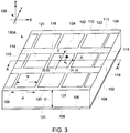
- FIG 3 is an expanded portion 100A of the RPD 100 shown in Figure 2 , in accordance with an embodiment.
- the expanded portion is represented by a frame 112 shown in Figure 2 .
- the RPD 100 is shown aligned with an X, Y, Z Cartesian coordinate system 126.
- the expanded portion 100A includes the pixelated anodes 110 (e.g., the pixelated anodes 113, 114, 116, 118, 119, 122, 120).
- the pixelated anodes 113, 114, 116, 118, and 119 are aligned along an X-coordinate of the Cartesian coordinate system 126.
- the pixelated anodes 116, 120, and 122 are aligned along a Y-coordinate of the Cartesian coordinate system 126.
- the expanded portion 100A includes sidewalls 101 of the semiconductor plate 102.
- the sidewalls 101 have a thickness D, which is aligned along the Z-coordinate between the first and second surfaces 104, 106.
- the expanded portion 100A of the RPD 100 includes an event 124.
- the photon 141 is absorbed by the pixelated anode 116 creating the event 124.
- the pixelated anodes 114, 118 are adjacent to the pixelated anode 116.
- the pixelated anodes 114, 118 are on opposing sides of the pixelated anode 116 along the X-coordinate.
- the event 124 is located at a coordinate of (x1, y, z) within the pixelated anode 116. The coordinates are determined relative to an origin position based on the pixelated anode 110, which absorbs the photon 141.
- the coordinate of the event 124 is based on a position relative to the pixelated anode 116.
- the values along the X and Y-coordinates are measured relative to an origin at a center of the pixelated anode 116.
- the value along the Z-coordinate is measured relative to the second surface 106.
- the zero value of the z coordinate is located on the intersection point between the Z-coordinate and the second surface 106.
- the point where the photon 141 is absorbed produces negative and positive charge clouds.
- the pixelated anode 116 collects electrons within the negative charge cloud to form the collected energy signal. For example, the negative charge cloud drifts towards the pixelated anode 116 based on the high voltage bias between the cathode 108 and the pixelated anode 116.
- the pixelated anodes 114, 118 adjacent to the pixelated anode 116 generate an adjacent energy signal.
- the adjacent energy signal is produced by the induction of the electrical charge signal as the negative charge cloud drifts towards the pixelated anode 116.
- the collected energy signal weakly depends and/or is independent on a location of the event 124 along the X and Y-coordinates of the pixelated anode 116.
- the adjacent energy signal depends on the location of the event 124 along the X and Y-coordinates of the pixelated anode 116. It may be noted as described herein a sum of the adjacent energy signals from adjacent pixels located symmetrically on both sides of the collecting pixel. For example, the pixelated anodes 114 and 118 are adjacent to the pixelated anode 116, which is the location of the event 124.
- the location of the event weakly depends and/or is independent on the location of the event 124 along the X and Y coordinates of the pixelated anode 116.
- the collected energy signal and the adjacent energy signal depend on the location of the event 124 along the Z-coordinate.
- the location of the event 124 along the Z-coordinate corresponds to the DOI of the event 124.
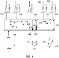
- Figure 4 is a side view of the expanded portion 100A, in accordance with an embodiment.
- the side view represents a cross-section along the line A-A' shown in Figure 3 .
- the event 124 is located at a coordinate (x1, y, z).
- the y coordinate is not specified.
- the collected energy signal and the adjacent energy signal are independent of the location of the event 124 along the Y-coordinate.
- the X coordinate is measured relative to the center of the pixelated anode 116.
- the location of the event 124 being at the second surface 106 corresponds to a z coordinate of zero.
- the point where the photon 141 is absorbed produces the negative and positive charge clouds.
- the negative and positive charge clouds correspond to electrical charges -q and +q, respectively.
- the electrical charge signal of the negative and positive charge clouds are proportional to the energy of the photon 141 absorbed by the pixelated anode 116.
- the collected energy signal of the pixelated anode 116 and the adjacent energy signal of the pixelated anodes 114, 118 are generated by the drift of the negative charge cloud towards the pixelated anodes 110 and the drift of the positive charge cloud toward the cathode 108.
- the amount of the electrical charge signal that the positive and negative charge clouds contribute (e.g., by induction) to the collected and adjacent energy signals are proportional to a length of the distance that the charge clouds travel toward the pixelated anode 110 and the cathode 108, respectively. It may be noted that the potential of the pixelated anodes 110 and the cathode 108 is based on the -HV bias supplied to the cathode 108.
- a type of the semiconductor plate 102 may affect a rate of drift of the positive and negative charge clouds.
- the semiconductor plate 102 can include CZT, which reduces a mobility of the positive charge cloud relative to the negative charge cloud.
- the positive charge cloud may be static. Accordingly, the positive charge cloud may not contribute to the electrical charge signal of the collected and adjacent energy signals.
- the collected and adjacent energy signals may be based only on the negative electron cloud.
- the -HV bias on the cathode 106 may be configured to generate an electrical field within the semiconductor plate 102 to be free of electron traps.
- the -HV bias allows the negative charge cloud to drift along a drift path 145 from the cathode 108 to the pixelated anode 116 along a distance "D" enabling a complete charge collection.
- the complete charge collection occurs when all of the electrons of the negative charge cloud is absorbed by the pixelated anode 110.
- a rate that the negative charge cloud drifts along the drift path 145 to the pixelated anode 116 is shorter than an electron lifetime ⁇ of the electrons of the negative charge cloud. Based on the rate, all of the electrons are absorbed by the pixelated anode 116, which represents the complete charge collection.
- the complete charge collection of the collected energy signal is equal to the induced charge of the electron in the negative charge cloud generated by the event 124. Additionally, the complete charge collection is proportional to the distance "D" traversed by the negative charge cloud along the drift path 145 of the negative charge cloud. Concurrently as the negative charge cloud traverses along the drift path 145, an electrical charge is induced on the pixelated anodes 114, 118. The electrical charge induced on the pixelated anodes 114, 118 represents the adjacent energy signal. The adjacent energy signal is proportional to the distance D. It may be noted that the electrons of the negative charge cloud are not collected by the pixelated anodes 114 and 118.
- the location of the event 124 relative to the pixelated anode 116 is more proximate relative to the pixelated anodes 114, 118.
- the pixelated anodes 114, 118 are remote relative to the location of the event 124 compared to the pixelated anode 116.
- both the collected and adjacent energy signals of the event 124 are proportional to the distance "D" that the negative charge cloud traverses along the drift path 145.
- Each of the pixelated anodes 114, 116, 118 have different solid viewing angles relative to the event 124. For example, a solid viewing angle of the pixelated anodes 114, 118 is smaller relative to a solid viewing angle of the pixelated anode 116.
- the viewing angles of the pixelated anode 116 are dependent on a value of a Z-coordinate and weakly dependent along the X and Y-coordinates of the event 124.
- the solid viewing angle of the Z-coordinates to collecting anode 116 is weakly dependent and/or independent on the location of event 124 along the X and Y coordinates.
- the solid viewing angles from the event 124 to adjacent non-collecting anodes 114 and 118 are dependent on the location of event 124 along the X-coordinate but, are weakly dependent and/or independent on the Y-coordinate of the event 124. Accordingly, the solid viewing angles of the pixelated anodes 114, 116, 118 weakly depend and/or are independent on the location of the event 124 along the Y-coordinate.
- the solid viewing angle of the pixelated anodes 114, 116, 118 depend on the value along the Z-coordinate, which is equal to the DOI.
- the electrical charge induced on the pixelated anodes 110 of the RPD 100 is proportional to an integral along coordinate Z, in a range starting from the location of the event 124 and ending at the corresponding pixelated anode 110.
- the integral is calculated over the solid viewing angles as a function of the Z-coordinates along the trajectory of the negative charge cloud to the corresponding pixelated anode 110.
- the location of the event 124 in the pixelated anode 116 For example, the location of the event 124 in the pixelated anode 116.
- the electrical charge induced on the pixelated anodes 116 represents the integral from the location where event 124 was created (e.g., located at the absorption location of photon 141) and ends at the pixelated anode 116 along the Z-coordinates.
- the integral is performed over the viewing angles from the event 124 to the pixelated anode 116 as a function of Z (e.g., DOI) along the drift path 147 of the negative charge cloud.
- the collected energy signal induced on the pixelated anode 116 is independent on the location of event 124 along the X-Y plane and the adjacent energy signals induced on the adjacent pixelated anodes 114, 118 are dependent on the location of the event 124 along the X-coordinate, but are independent on the Y-coordinate.
- the variable V 118 of Equation 1 represents the adjacent energy signal of the pixelated anode 118 as a function of a value of the X-coordinate measured from the center of the pixelated anode 116.
- the variable V 114 of Equation 2 represents the adjacent energy signal of the pixelated anode 114 as a function of a value of the X-coordinate measured from the center of pixelated anode 116.
- the constant ⁇ represents the linearity coefficient of the RPD 100.
- the adjacent energy signals defined in Equations 1 and 2 have positive and negative linearity coefficients, respectively.
- the electrical charges induced on the pixelated anodes 114, 118 depend on the location of the event 124 along the X-coordinate.
- V 114 + V 118 2 ⁇ V o
- the collected energy signal from the pixelated anode 116 and the sum of the adjacent energy signals from the pixelated anodes 114, 118 are both independent on the location of the event 124 along the X and Y-coordinates, but depend on the location along the Z-coordinate.
- the dependency of the collected energy signal on the location of the event 124 along the Z-coordinate, representing the DOI, is undesired and produces the low energy tail.
- the low energy tail is produced when photons having the same energy produce different induced charges on the collected energy signal based on the DOI.
- the low energy tail is measured by the RPD 100 at different energies and appear as a tail in an energy spectrum that is remote from a peak of the energy spectrum.
- a difference between the collected energy signal and the sum of the adjacent energy signals (e.g., measures by the adjacent pixelated anodes 114, 118) is represented as the variable ⁇ V, in Equation 4.
- the difference between the collected energy signal and the sum of the adjacent energy signals can be used to reduce the low energy tail.
- the variable V 116 of Equation 4 represents the collected energy signal, and the variables V 114 and V 118 represents the adjacent energy signals of the pixelated anodes 114, 118, respectively.
- the variable C represents the adjusting factor.
- the adjusting factor may range from values larger, smaller, and/or equal to one.
- the photons for a plurality of events along a range are absorbed by the RPD 100.
- the range is along the Z-coordinate.
- the range represents where the photons are absorbed in the RPD 100 above the cathode 108.
- the range represents when the sum of the solid viewing angles of the adjacent pixelated anodes 114 and 118 are approximately the same as the viewing angle of collecting pixel 116.
- the absorption of the photons are distant relative to the pixelated anodes 114, 116, 118, which produces the solid viewing angle of the pixelated anode 116 that is approximately equal to the sum of the solid viewing angles of pixelated anodes 114 and 118.
- the electrical charges of the pixelated anodes 114, 116, 118 produces a difference (e.g., ⁇ V ) equal to zero. Additionally or alternatively, the difference (e.g., ⁇ V ) is not equal to zero at a second range when the negative charge cloud drifts towards the pixelated anodes 114, 116 and 118.
- the expanded portion 100A of Figure 3 includes a second event 125.
- the second event 125 is at a location having coordinates (P/2- ⁇ x, y, z).
- the y coordinate is not specified.
- the collected energy signal and the adjacent energy signal are independent of the location of the second event 125 along the Y-coordinate.
- the X-coordinate is measured relative to the center of the pixelated anode 116.
- the location of the second event 125 being at the second surface 106 corresponds to a Z-coordinate of zero.
- the line 144 is a symmetry line between the pixelated anodes 116, 118.
- the symmetry line defines a separation between the two adjacent pixelated anodes 116, 118.
- the line 144 is located at a distance P/2 from the center of the pixelated anode 116.
- the resulting event represent a charge sharing event.
- the negative charge cloud resulting from the absorbed photon (e.g., the event) is divided between the two adjacent pixelated anodes 116, 118.
- a portion of the negative charge cloud positioned on a left side of the line 144 (e.g., positioned within the pixelated anode 116) is drifted toward the pixelated anode 116.
- a portion of the negative charge cloud positioned on a right side of the line 144 (e.g., positioned within the pixelated anode 118) is drifted toward the pixelated anode 118.
- the charge induced by the negative charge cloud on the pixelated anode 116, 118 is split. The split charge collected by the pixelated anodes 116, 118 can be recovered as an event in one of the pixelated anodes 116, 118.
- the location of the second event 125 is removed from the line 144 by a distance of ⁇ x.
- the distance is larger than a diameter of the negative charge cloud, and does not represent the charge sharing event.
- the electrons of the negative charge cloud is not shared between the adjacent pixelated anodes 116, 118.
- the negative charge cloud formed at the second event 125 traverses along a drift path 147.
- the drift path 147 extends a distance "D" between the first and second surfaces 104, 106.
- all of the charge from the negative charge cloud is collected by the pixelated anode 116.
- the pixelated anode 116 has the complete charge collection for the second event 125.
- the second event 125 induces a charge on the adjacent pixelated anodes 114, 118.
- the location of the second event 125 is more proximate to the pixelated anode 118 relative to the pixelated anode 114.
- the solid viewing angles of the pixelated anodes 114, 118 are different.
- the induced charge on the pixelated anode 118 is greater than the pixelated anode 114.
- the expanded portion 100A includes a third event 117.
- the third event 117 is at a location having coordinates (P/2- ⁇ x, y, zi).
- the Y-coordinate is not specified.
- the collected energy signal and the adjacent energy signal are independent of the location of the third event 117 along the Y-coordinate.
- the X-coordinate is measured relative to the center of the pixelated anode 116.
- the negative charge cloud formed by the third event 117 drifts towards the pixelated anode 116. Similar to the second event 125, the negative charge cloud of the third event 117 drifts along the drift path 147. However, the locations representing the DOI of the second and third events 125, 117 are different along the Z-coordinate of the events 125, 117. For example, the negative charge cloud of the third event 117 drifts a shorter distance along the drift path 147 relative to the negative charge cloud of the second event 125. Based on the difference in positions along the Z-coordinate, the charges on the pixelated anodes 114, 116, 118 are different. For example, the charge of the pixelated anode 116 and the induced charge on the pixelated anodes 114, 118 will be smaller for the third event 117 relative to the second event 125.
- a charge of the negative charge clouds of the second and third events 125, 117 are the same.
- the difference in locations of the second and third events 125, 117 along the Z-coordinate adjusts the charges collected by the pixelated anodes 114, 116, 118.
- the difference in locations of the events 125, 117 along the Z-coordinates have different DOIs.
- the difference in charge collected by the pixelated anode 116 between the second and third events 125, 117 forms the low-energy tails of the energy spectrum of the RPD 100.
- the difference between the collected energy signal and the sum of the adjacent energy signals can be used, which is independent on the locations (e.g., independent of the DOI) of the events (e.g., the event 124, the second event 125, the third event 117).
- the difference can be used as a signal of events to produce a spectrum of the RPD 100 to reduce low energy tails.
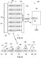
- FIG. 5 is a schematic illustration 220 of an embodiment of the RPD 100 having the electronic channels 111 operably coupled to a controller circuit 136, in accordance with an embodiment.
- the schematic illustration 220 includes a readout unit 132 and a memory 138.
- the electronic channel 111 may include one or more processors.
- the electronic channels 111 may include a central processing unit (CPU), one or more microprocessors, or any other electronic component capable of processing input data according to specific logical instructions.
- the electronic channels 111 may include and/or represent one or more hardware circuits (e.g., analog components) or circuitry that include, are connected with, or that both include and are connected with one or more processors, controllers, and/or other hardware logic-based devices. Additionally or alternatively, the electronic channels 111 may execute instructions stored on a tangible and non-transitory computer readable medium.
- the pixelated anodes 110 of the RPD 100 are electrically and/or operably coupled to the electronic channels 111 via interconnections 131.
- the interconnections 131 are configured to clamp a voltage potential of the pixelated anodes 110 to be equal to a virtual ground (e.g., approximately zero) of charge sensitive pre-amplifiers (CSP) 109, shown in Figure 6 .
- CSP charge sensitive pre-amplifiers
- the electronic channels 111 receive the electrical charge signals measured by the pixelated anodes 110 via the interconnections 131.
- the electronic channels 111 are electrically and/or operably coupled to the readout unit 132.
- the readout unit 132 is configured to collect the voltage signals received from the electronic channels 111, and to convert the analog values of the voltage signals into digital values.
- the readout unit 132 may include analog to digital converters.
- the readout unit 132 may be integrated with the electronic channels 111 and/or the controller circuit 136.
- the readout unit 132 is configured to generate a digital addresses associated with each of the digital values. The digital address corresponds to one of the pixelated anodes 110 that generated an electrical charge signal in response to the event.
- the readout unit 132 is configured to generate a data packet 146 representative of the voltage signals.
- the data packet 146 may include a header 143 containing an address representing a location of the pixelated anode 110 on the RPD 100.
- the data packet 146 includes a payload 149.
- the payload 149 includes the digital values generated by the readout unit 132 representative of the voltage signal produced by the pixelated anode 110.
- the data packets 146 are transmitted from the readout unit 132 via a port 134 to the controller circuit 136 and stored in the memory 138.
- the controller circuit 136 may include a central processing unit (CPU), one or more microprocessors, or any other electronic component capable of processing input data according to specific logical instructions.
- the controller circuit 136 may include and/or represent one or more hardware circuits or circuitry that include, are connected with, or that both include and are connected with one or more processors, controllers, and/or other hardware logic-based devices. Additionally or alternatively, the controller circuit 136 may execute instructions stored on a tangible and non-transitory computer readable medium (e.g., the memory 138).
- the data packets 146 in the memory 138 are analyzed by the controller circuit 136.
- the controller circuit 136 is configured to execute one or more models and/or algorithms stored in the memory 138 that may include, charge-sharing correction, low-energy tail correction, image reconstruction, and/or the like as described herein to process the digital values and generate the image data.
- FIG. 6 is a schematic illustration of the operations performed by the electronic channels 111, in accordance with an embodiment.
- the electronic channels 111 is shown performing a plurality of operations shown as the CSP 109, a shaper circuit 135, thresholding circuit 137, amplifier circuit 139, and a peak and hold (P&H) circuit 200 to process the electrical charge signals received from the interconnections 131.
- the operations may correspond to operations performed by one or more processors by the electronic channels 111 and/or be configured hardware (e.g., ADC converters, amplifiers, filters) of the electronic channels 111.
- the CSP 109 is configured to integrate the electrical charge signal from the pixelated anodes 110.
- An integrated signal 203 is representative of an integrated electrical charge signal by the CSP 109.
- the electrical charge signal is integrated over time 201 by the CSP 109 to define the integrated signal 203.
- the integrated signal 203 reaches a steady state value 202.
- the steady state value 202 represents the total induced charge collected by the pixelated anodes 110.
- the lowest potential of the pixelated anode 110 for example, is determined by the CSP 109, which is configured to clamp the potential of the pixelated anodes 110 to a voltage that is equal and/or similar to the voltage of the virtual ground of the CSP 109.
- the integrated signal 203 is passed to the shaper circuit 135.
- the shaper circuit 135 is configured to filter the integrated signal 203 (e.g., band-pass filter) to increase a signal to noise ratio of the integrated signal 203.
- the filtering by the shaper circuit 135, changes the integrated signal 203 to form a filtered signal 205 (e.g., a Gaussian shape having an amplitude 204).
- the filtered signal 205 is passed to the threshold circuit 137.
- the threshold circuit 137 is configured to pass the amplitude 204 of the filtered signal 205 to the amplifier circuit 139 when the amplitude 204 is above a predetermined non-zero threshold, or to block the amplitude 204 when the amplitude 204 is below the predetermined non-zero threshold.
- An amplitude 206 of a thresholded signal 207 may be equal to or larger than the amplitude 204 of the filtered signal 205, which depends on the amplification of the threshold circuit 137.
- the thresholded signal 207 is passed to the amplifier circuit 139.
- the amplifier circuit 139 is configured to amplify the thresholded signal 207 by increasing the amplitude 206. For example, the amplifier circuit 139 increases the amplitude 206 of the thresholded signal 207 to form an amplified signal 209 having an increased amplitude 208.
- the amplified signal 209 is passed to the P&H circuit 200.
- the P&H circuit 200 is configured to amplify the amplified signal 209 to hold a maximum value of the amplified signal 209 corresponding to and/or about the amplitude 208 to form the voltage signal 211.
- the voltage signal 211 includes a rising portion 215 and a peak value 213. The peak value may be similar to and/or about the amplitude 208.
- the voltage signal 211 is received by the readout unit 132.
- the payload 149 of the data packet 146 includes digital values of the peak value 213 of the voltage signal 211, which is stored later in the memory 138.
- the payload 149 may include the amplitudes 202, 204, 206, 208 of the signals 203, 205, 207, 209, respectively.
- the peak value 213 of the pixelated anodes 110 is a representation of the electrical charge of the photon absorbed by the RPD 100.
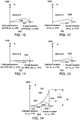
- Figure 7 is a graphical illustration 150 of an induced charge on the collecting pixelated anode 116 based on a distance traversed by a negative charge cloud, in accordance with an embodiment.
- the distance traversed by the negative charge cloud along the drift path 145 is along the Z-coordinate from the cathode 108 to the pixelated anode 116.
- a direction of the drift is shown as a direction of an arrow 152.
- the negative charge cloud is formed by the absorption of the photon 141 in the pixelated anode 116.
- the charge on the collecting pixelated anode 116 is independent on the location of the event 124 along the X and Y-coordinates.
- the independency of the charge is based on the solid viewing angles. Different (x, y) locations of events within the pixelated anode 116 have similar viewing angles to the pixelated anode 116 from the different locations of the events 124, 125, 117. Accordingly, the different locations of the events, along the X and Y-coordinates have the same and/or similar solid viewing angles with respect to the pixelated anode 116. Based on the independency relative to the X and Y-coordinates, the location of the event 124 at (x, y) of the pixelated anode 116 are not shown in the graphical representation 150.
- a line 160 indicates the location of the event 124 along the Z-coordinate.
- a line 157 indicates a location of the pixelated anode 116.
- Collected energy signals 154, 156, 158 illustrate different charges of the pixelated anode 116 based on a distance the negative charge cloud drifts from the cathode 108 the pixelated anode 116.
- the collected energy signals 154, 156, 158 represent signals measured by the pixelated anode 116 having different dimensions of the pixelated anode 116.
- the collected energy signals 154, 156, 158 collected by the pixelated anode 116 having different dimensions WxW relative to the thickness "D" of the semiconductor 102.
- the pixelated anode 116 of the collected energy signal 154 has dimensions WxW that are larger than the thickness "D" of the RPD 100. For example in the collected energy signal 154, an aspect ratio of the dimensions W/D is greater than one.
- the charge of the collected energy signal 154 is shown increasing linearly as the negative charge cloud traverses to the pixelated anode 116.
- the pixelated anode 116 of the collected energy signal 156 has dimensions WxW representing an aspect ratio W/D that is equal to 0.5.
- the charge of the collected energy signal 156 is shown increasing non-linearly as the negative charge cloud traverses to the pixelated anode 116.
- the pixelated anode 116 of the collected energy signal 158 has dimensions WxW that are less than the thickness "D" of the RPD 100. For example, a ratio of the dimensions WxW representing aspect ratio W/D that is less than 0.5.
- the charge of the collected energy signal 158 is shown increasing exponentially as the negative charge cloud traverses to the pixelated anode 116.
- FIGS 8 and 9 are graphical illustrations 180, 240 of collected energy signals 156, 186 and adjacent energy signals 166, 188, in accordance to embodiments herein.
- the collected energy signals 156, 186 represent charges (e.g., Q shown along the vertical axes) measured at the pixelated anode 116.
- the adjacent energy signals 186, 188 represent induced charges collected by the pixelated anode 118, which is adjacent to the pixelated anode 116.
- the collected energy signals 156, 186 and the adjacent energy signals 166, 188 show changes in the charge received by the pixelated anodes 116, 118 along the Z-coordinate.
- the charge of the collected energy signals 156, 186 and the adjacent energy signals 166, 188 increases as the negative charge cloud traverses towards the pixelated anodes 116, 118, which is shown along the arrow 152.
- the collected energy signal 156 is based on the second event 125.
- the negative charge cloud is formed at the location (e.g., P/2- ⁇ x, y, z) of the second event 125.
- the charge of the collected energy signal 156 increases as the negative charge cloud traverses towards the pixelated anode 116.
- the collected energy signal 156 ends at point 185 representing a position of the pixelated anodes 116, 118.
- a distance between the points 181, 185 represents the thickness "D" of the RPD 100.
- the collected energy signal 156 reaches a peak 193 at the point 185.
- the adjacent energy signal 166 is based on the second event 125.
- the adjacent energy signal 166 starts at the point 181 and ends at the point 185.
- the adjacent energy signal 166 represents the induced charge on the pixelated anode 118 based as the negative charge cloud drifts to the pixelated anode 116.
- the induced charge on the pixelated anode 118 increases as the negative charge cloud traverses from the cathode 108 to the pixelated anode 116. For example, as the negative charge cloud traverses along the drift path 147, the solid viewing angle increases with respect to the pixelated anode 118.
- the solid viewing angle of the pixelated anode 118 decreases. For example, as the negative charge cloud traverses to the pixelated anode 116 a distance between the negative charge cloud and the pixelated anode 118 changes. Between the points 181 and 199, the negative charge cloud traverses to the pixelated anode 116. The distance between the negative charge cloud and the pixelated anode 118 decreases. Based on the decrease in distance, the induced charge on the pixelated anode 118 increases reaching a peak 191. Subsequent to the point 199 as the negative charge cloud drifts to the pixelated anode 116, the distance between the negative charge cloud and the pixelated anode 118 increases.
- the increase in the distance further decreases the solid viewing angle of the pixelated anode 118.
- the decrease in the solid viewing angle decreases the induced charge on the pixelated anode 118.
- the charge induced on the pixelated anode 118 has a different polarity or negative charge.
- the change in polarity of the charge induced on the pixelated anode 118 occurs at the point 199.
- the peak 191 is formed by the adjacent energy signal 166.
- the peaks 193, 191 of the collected and adjacent energy signals 156, 166 are indicative of the peak value 213 determined by the P&H circuit 200 ( Figure 6 ) in the corresponding electronic channels 111.
- the digital values (e.g., within the payload 149) of the peaks 193,191 correspond to the peak value 213 stored in the memory 138 with corresponding addresses (e.g., within the header 143) representing the pixelated anodes 116, 118.
- the collected energy signal 186 ( Figure 9 ) represents the charge (e.g., Q shown along the vertical axis) measured at the pixelated anode 116.
- the collected energy signal 156 is based on the third event 117.
- the charge of the collected energy signal 186 increases as the negative charge cloud traverses towards the pixelated anode 116. Similar to the adjacent energy signal 156, the polarity of the induced charge changes at the point 199.
- the collected energy signal 186 ends at point 185 representing a position of the pixelated anodes 116, 118.
- the collected energy signal 186 reaches a peak 195 at the point 185.
- the collected energy signals 156, 186 have different magnitudes of charges measured by the pixelated anode 116.
- the collected energy signal 186 has a smaller electrical charge relative to the collected energy signal 156.
- the difference in electrical charges is based on the distance traversed by the negative charge clouds of the second event 125 and the third event 117, respectively.
- the negative charge cloud of the second event 125 traverses the thickness D of the RPD 100 to the pixelated anode 116.
- the negative charge cloud of the third event 117 traverses from the point 183 to the pixelated anode 116.
- the distance traversed by the negative charge cloud of the third event 117 is less than the distance traversed by the negative charge cloud of the second event 125.
- the charge on the pixelated anode 116 increases based on the distance traversed by the negative charge cloud along the Z-coordinate. Based on the difference in the distances, the peak 193 is higher relative to the peaks 195.
- the adjacent energy signal 188 is based on the third event 117.
- the adjacent energy signal 188 starts at the point 183 and ends at the point 185.
- the adjacent energy signal 188 represents the induced charge on the pixelated anode 118 based on the negative charge cloud formed at the location of the third event 117.
- the induced charge on the pixelated anode 118 increases as the negative charge cloud traverses to the pixelated anode 116. For example, as the negative charge cloud traverses along the drift path 147, the solid viewing angle increases with respect to the pixelated anode 118.
- the adjacent energy signal 188 ends at 185 with a negative charge.
- the negative charge cloud of the third event 117 traverses to the pixelated anode 116
- the charge induced on the pixelated anode 118 increases.
- the adjacent energy signal 188 reaches a peak 197.
- the solid viewing angle decreases and the distance of the negative charge cloud to the pixelated anode 118 increases.
- the charge induced on the adjacent energy signal 188 decreases.
- the charge induced on the pixelated anode 118 changes polarity and is negative.
- the adjacent energy signal 188 ends at a negative charge at the point 185.
- the difference in distances traversed by the negative charge clouds of the second and third events 125, 117 affects a magnitude of the peaks 191, 197.
- the peak 197 is smaller than the peak 191.
- a range of the adjacent energy signals 166, 188 are the same.
- the range of charge between the peak 191 and the point 185 of the adjacent energy signal 166 is equal to a range of charge between the peak 197 and the point 185 of the adjacent energy signal 188.
- An amount of negative charge induced on the pixelated anode 118, represented in the ranges, on the adjacent energy signals 166, 188 are the same.
- the adjacent energy signals may or may not end with a negative induced charge at the point 185.
- the peaks 195, 197 of the collected and adjacent energy signals 186, 188 are indicative of the peak value 213 determined by the P&H circuit 200 ( Figure 6 ) in the corresponding electronic channels 111.
- the digital values (e.g., within the payload 149) of the peaks 195, 197 correspond to the peak value 213 stored in the memory 138 with corresponding addresses (e.g., within the header 143) representing the pixelated anodes 116, 118.
- a difference between the peaks 193, 191 and 195, 197 of the collected and adjacent energy signals 156, 166 and 186, 188 represent a delta charge (e.g., ⁇ Q) 189, 187, respectively.
- the delta charge 189 between the peaks 193, 191 of the collected and adjacent energy signals 156, 166, respectively.
- the delta charge 189 corresponds to the third event 117 located at the point 183.
- the delta charges 187, 189 are based on different events 125, 117, however, both are approximately equal to each other.
- the delta charges 187, 189 based on the collected and adjacent energy signals 156, 188 and 186, 188 is independent of the location of the events 125, 117 along the Z-coordinate.
- the delta charges 187, 189 represent the difference, ⁇ V, as describe in Equation 4.
- a value of the difference (e.g., ⁇ V ) between the collected and adjacent energy signals 156, 186, 166, 188 is independent on the location of the events, for all the coordinates (x, y, z).
- the locations of the events 125, 117 are proximate to the pixelated anode 118 and remote from the pixelated anode 114 along the X-coordinate.
- the proximity of the events 125, 117 to the pixelated anode 118 represent a maximum and/or large charge induced on the pixelated anode 118 for the adjacent energy signals 166, 188.
- the induced signal on pixelated anode 114 is minimal and/or small.
- the sum of the adjacent energy signals from the pixelated anodes 114 and 118 is fixed and/or is equal to 2V 0 .
- the sum of the adjacent energy signals from the pixelated anodes 114, 118 is about equal to the signal from the pixelated anode 118 alone.
- the adjacent energy signal 166, 188, received only from the pixelated anode 118 for the events 125 and 117 is approximately equal to the sum of the adjacent energy signals received from the pixelated anodes 114, 118.
- the delta charges 187, 189 represent a difference of the collected energy signal of the pixelated anode 116 and the sum of the adjacent energy signals of the pixelated anodes 114, 118 (e.g., based on Equation 4). Thereby the delta charges 187, 189 are independent of the locations of the events 125, 117 along all the coordinates (x, y, z).
- the collected and adjacent energy signals 156, 166 are the same from the point 181 to the point 199.
- the collected and adjacent energy signals 186, 188 are the same from the point 183 to the point 199.
- the charge deltas 187, 189 can be calculated based on integrals of the collected energy signals 156, 186.
- the charge delta 187 for the third event 117 is equal to an integral along the Z-coordinate of the collected energy signal 186 between the points 199 and 185.
- the charge delta 189 for the second event 125 is equal to an integral along the Z-coordinate of the collected energy signal 156 between the points 199 and 185.
- the morphology (e.g., slope, shape) of the collected energy signals 156, 186 are the same, but are vertically displaced with respect to each other.
- the charge deltas 187, 189 determined based on the integrals of the collected energy signals 156, 186 are equal to each other, and are independent of the locations of the events 125, 117.
- the delta charges 187, 189 is equal to the integral along the Z-coordinate of the collected energy signals 156, 186 regardless of the locations of the events 125, 117.
- the difference between the collected and adjacent energy signals 156, 166 and 186, 188 is equal to zero between the points 181, 199 and the points 183, 199, respectively. Subsequent to the point 199, the difference of the collected and adjacent energy signals 156, 166 and 186, 188 is not equal to zero.
- Figures 10-14 are graphical representations of the collected and adjacent energy signals measured at the pixelated anodes 114, 116, 118, in accordance with embodiments herein.
- Figures 10-13 illustrate changes in the induced charge on the adjacent pixelated anodes 114, 118 as the negative charge cloud traverses along the Z-coordinate.
- the pixelated anodes 114, 116, 118 have dimensions WxW when W is half of the thickness "D" of the RPD 100. For example, the aspect ratio of D/W is 0.5.
- FIG 10 is a graphical representation 1000 of the adjacent energy signal 166, in accordance with an embodiment.
- the adjacent energy signal 166 is similar to and/or the same as the adjacent energy signal 166 shown in Figure 8 .
- the adjacent energy signal 166 represents the induced charge on the pixelated anode 118.
- the adjacent energy signal 166 is based on the second event 125 ( Figure 4 ).
- the adjacent energy signal 166 represents the induced charge as the negative charge cloud traverses along the drift path 147 to the pixelated anode 116 from the cathode 108.
- the adjacent energy signal 166 extends along the horizontal axis in the direction of the arrow 152 representing the movement of the negative charge cloud.
- the adjacent energy signal 166 extends from a zero coordinate representing the location of the second event 125 to the width "D" of the RPD 100 along the Z-coordinate.
- FIG 11 is a graphical representation 1100 of the adjacent energy signal 250, in accordance with an embodiment.
- the adjacent energy signal 250 represents the induced charge on the pixelated anode 114.
- the adjacent energy signal 250 is based on the second event 125 ( Figure 4 ).
- the adjacent energy signal 250 represents the induced charge as the negative charge cloud traverses along the drift path 147 to the pixelated anode 116 from the cathode 108.
- the adjacent energy signal 250 extends along the horizontal axis in the direction of the arrow 152 representing the movement of the negative charge cloud.
- the adjacent energy signal 250 extends from a zero coordinate representing the location of the second event 125 to the width "D" of the RPD 100 along the Z-coordinate.
- the location of the second event 125 is positioned proximate to the pixelated anode 118.
- the location of the second event 125 along the X-coordinate relative to the center of pixelated anode 116 is at P/2- ⁇ x.
- the location of the second event 125 along the X-coordinate relative to the center of pixelated anode 116 is at - (P/2- ⁇ x).
- the second event 125 is located a distance of ⁇ x from the pixelated anode 118, which is remote from the pixelated anode 114 at a distance of P- ⁇ x.
- an induced charge on the adjacent energy signal 166 received from the pixelated anode 118 is greater than the induced charge on the adjacent energy signal 250 received from the pixelated anode 114.
- FIG 12 is a graphical representation 1200 of the adjacent energy signal 1202, in accordance with an embodiment.
- the adjacent energy signal 1202 represents the induced charge on the pixelated anode 118.
- the adjacent energy signal 1202 is based on the event 124 ( Figure 4 ).
- the adjacent energy signal 1202 represents the induced charge as the negative charge cloud traverses along the drift path 145 to the pixelated anode 116 from the cathode 108.
- the adjacent energy signal 1202 extends along the horizontal axis in the direction of the arrow 152 representing the movement of the negative charge cloud.
- the adjacent energy signal 1202 extends from a zero coordinate representing the location of the event 124 to the width "D" of the RPD 100 along the Z-coordinate
- FIG 13 is a graphical representation 1300 of the adjacent energy signal 1302, in accordance with an embodiment.
- the adjacent energy signal 1302 represents the induced charge on the pixelated anode 114.
- the adjacent energy signal 1302 is based on the event 124 ( Figure 4 ).
- the adjacent energy signal 1302 represents the induced charge as the negative charge cloud traverses along the drift path 145 to the pixelated anode 116 from the cathode 108.
- the adjacent energy signal 1302 extends along the horizontal axis in the direction of the arrow 152 representing the movement of the negative charge cloud.
- the adjacent energy signal 1302 extends from a zero coordinate representing the location of the event 124 to the width "D" of the RPD 100 along the Z-coordinate
- the location of the event 124 along the X-coordinate relative to the center of pixelated anode 116 is at -x1.
- the event 124 is located a distance of x1 from the pixelated anode 118, and a distance of - x1 from the pixelated anode 114.
- the value of x1 is zero, the induced charges on the adjacent energy signals 1202, 1302 are equal to each other.
- FIG 14 is a graphical representation 1400 of adjacent energy signals 252 and the collected energy signal 156, in accordance with an embodiment.
- the collected energy signal 156 is similar to and/or the same as the collected energy signal 156 shown in Figures 7-8 .
- the adjacent energy signals 252 is a sum of the adjacent energy signals 166, 250 and/or 1202, 1302.
- a sum of the adjacent energy signals 166, 250 and/or 1202, 1302 is independent along the X and Y-coordinates of the locations of the events 124, 125.
- the sum of the adjacent energy signals 166, 250 and/or 1202, 1302 is independent on a location (x, y) of the events 124, 125.
- the collected and adjacent energy signals 156, 252 are independent on the location (x, y) of the events 124, 125.
- the collected and adjacent energy signals 156, 252 have a dependency along the Z-coordinate, which is represented as a horizontal axis in Figure 14 .
- a delta charge 1402 is shown between the peak 193 of the collected energy signal 156 and a peak 1404 of the adjacent energy signals 252.
- the delta charge 1402 is independent along the X, Y, and Z-coordinates.
- a morphology of the collected and adjacent energy signals 156, 252 changes.
- the collected and adjacent energy signals 156, 252 are identical until a distance 258 along the Z-coordinate.
- the electrical charge on the pixelated anode 116 is the same and/or similar value as the sum of the adjacent energy signals 252 of the pixelated anodes 114 and 118.
- the difference ⁇ V between the collected energy signal 156 and the adjacent energy signals 256 is zero.
- the morphology of the collected and adjacent energy signals 156, 252 changes.
- the charge (e.g., along the vertical axis) of the collected energy signal 156 increases.
- the induced charge of the adjacent energy signals 252 decreases and/or changes polarity.
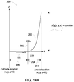
- Figure 14A is a graphical illustration 260 of a delta charge (e.g., ⁇ Q 1 ) waveform 262.
- the delta charge waveform 262 represents a difference between the collected energy signal 156 and the adjacent energy signals 252.
- the delta charge waveform 262 is divided into two ranges 266, 264 based on a distance from the cathode 108.
- the range 266 extends along the horizontal axis from the cathode 108 to the distance 258.
- the collected and adjacent energy signals 156, 252 are the same from the cathode 108 to the distance 258.
- the collected and adjacent energy signals 156, 252 are the same corresponding to the delta charge equal to zero.
- the range 264 extends along the horizontal axis from the distance 258 to the pixelated anodes 114, 116, 118 (e.g., at a distance "D" along the Z-coordinate).
- the morphologies of the collected and adjacent energy signals 156, 252 change subsequent to the distance 258 along the horizontal axis.
- the delta charge waveform 262 increases exponentially and/or rapidly in the direction of the arrow 152.
- the negative charge cloud contributes to the delta charge after traversing the distance 258.
- the negative charge cloud continually contributes to the delta charge until reaching the pixelated anode 116 at the distance "D" along the Z-coordinate.
- the photons corresponding to the events 117, 124, 125 are absorbed in the range 266, by the pixelated anodes 114, 118 as the induced energy charge.
- the delta charge ( ⁇ Q 1 ) is constant and is independent on the location of the events 117, 124, 125 (e.g., (x, y, z) coordinates).
- the viewing angle of the pixelated anodes 114, 118 of the event 124 weakly depends on the values of the Y-coordinates. Further to reduce the dependency of the viewing angle, on Y-coordinate of the event 124 can be achieved by including additional adjacent pixelated anodes. For example, the sum of the adjacent energy signals may be acquired by summing the adjacent energy signals from all or part of the adjacent pixelated anodes 114, 118, 120, 121, 122, 123, 127, 129 ( Figure 3 ) that are adjacent to the pixelated anode 116 that includes the event 124.
- the sum may be determined by the controller circuit 136 as a linear combination of the adjacent energy signals from the pixelated anodes 114, 118, 120, 121, 122, 123, 127, 129 that are directly adjacent to and/or surround the pixelated anode 116.
- the sum of the linear combination as mentioned above is less dependent on the X and Y-coordinates of the event 124 within the pixelated anode 116. Additionally or alternatively, a sum of the viewing angles of the pixelated anodes 114, 118, 120, 121, 122, 123, 127, 129 relative to the event 124 is independent on the location (x, y) of the event 124.
- Equation (4a) V 116 ⁇ C ⁇ k 114 ⁇ V 114 + k 118 ⁇ V 118 + k 120 ⁇ V 120 + k 121 ⁇ V 121 + k 122 ⁇ V 122 + k 123 ⁇ V 123 + k 127 ⁇ V 127 + k 129 ⁇ V 129
- the variable C is the adjusting factor as described in Equation 4.
- the variables V 114 , V 118 , V 120 , V 121 , V 122 , V 123 , V 127 , V 129 represent the adjacent energy signals measured by the pixelated anodes 114, 118, 120, 121, 122, 123, 127, 129, respectively.
- the variable V 116 represents the collected energy signal measured by the pixelated anode 116.
- the variables k 114 , k 118 , k 120 , k 121 , k 122 , k 123 , k 127, k 129 represent factors configured to adjust the adjacent energy signals of the pixelated anodes 114, 118, 120, 121, 122, 123, 127, 129.
- the variables k 114 , k 118 , k 120 , k 121 , k 122 , k 123 , k 127, k 129 may have a value equal to and/or greater zero determined during calibration of the RPD 100.
- the value of the difference ⁇ V given by Equation 4a above may be equal to and/or be adjusted to be equal to zero based on the values of the adjusting factor (e.g., C ) and the factors (e.g., k 114 , k 118 , k 120 , k 121 , k 122 , k 123 , k 127, k 129 ).
- the adjusting factor e.g., C
- the factors e.g., k 114 , k 118 , k 120 , k 121 , k 122 , k 123 , k 127, k 129 .
- the collected energy signal e.g., V 116
- the adjusted sum of the pixelated anodes 114, 118, 120, 121, 122, 123, 127, 129 e.g., C ⁇ ( k 114 ⁇ V 114 + k 118 ⁇ V 118 + k 120 ⁇ V 120 + k 121 ⁇ V 122 + k 127 ⁇ V 127 + k 129 ⁇ V 129
- C ⁇ ( k 114 ⁇ V 114 + k 118 ⁇ V 118 + k 120 ⁇ V 120 + k 121 ⁇ V 122 + k 127 ⁇ V 127 + k 129 ) have the same value and the same dependency on the Z-coordinates. For example, within the range most of the photons are absorbed in the RPD 100.
- the collected energy signal and the adjusted sum of the adjacent energy signals are the same for all the events within the pixelated anode 116. Thereby, all the events within the pixelated anode 116 will produce the same signal ⁇ V regardless on the location of the event along coordinates (x, y, z).
- Figures 15-19 since the delta charge is independent of the coordinates (x, y, z) of the event, the controller circuit 136 utilizes the delta charge to reduce the low energy tail of a spectrum.
- Figures 15- 18 are graphical representations of spectrums of measured electrical charges. The spectrums are based on RPD 100 that have been calibrated for gain and offsets using measurements by two isotopes.
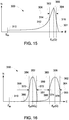
- FIG. 15 is a graphical illustration 300 of a spectrum 301, in accordance with an embodiment.
- the spectrum 301 is based on a number of events (e.g., the events 124, 125, 117) acquired from one of the pixelated anodes 110, such as the pixelated anode 116, of the RPD 100.
- the number of events is shown along the vertical axis.
- An energy for the number of events is shown along the horizontal axis.
- the spectrum 301 may represent a combination of collected energy signals for at least one event.
- the spectrum 301 is not corrected for charge sharing events and/or correction of the low energies tail.
- the spectrum 301 may be based on a number of events acquired by the pixelated anode 116.
- the spectrum 301 includes a peak 308 positioned at an energy value of E p (Q).
- the peak 308 represents an energy level for a largest number of events measured by the controller circuit 136.
- the spectrum 301 includes a low energy tail 312 extending from 310 to an energy at 314.
- the value of the spectrum 301 at 310 may be based on the predetermined non-zero threshold of the threshold circuit 137.
- the value of the spectrum 301 at 310 may correspond to charges measured by the controller circuit 136 that are above the predetermined non-zero threshold.
- the low energy tail is formed by the different locations of the at least one events (e.g., DOI) within the pixelated anode 116.
- the spectrum 301 includes a width 306 (e.g., ⁇ E 1 ) extending from the energies at 302 to 304 representing a full-width-half-maximum (FWHM) of the spectrum 301.
- the width 306 may be defined at half of a height of a number of events of the peak 308. For example, the width correspond to half of the number of events of the peak 308.
- the width 306 may be formed by an electrical noise, which affects the charge measured during the at least one event of the first pixel. The electrical noise may be generated by the RPD 100, the electronic channels 111, and/or the like.
- Figure 16 is a graphical illustration 350 of an embodiment of a spectrum 351 and a corrected energy spectrum 353.
- the spectrum 351 is based on collected and adjacent energy signals for a plurality of events.
- the spectrum 351 represents a number of events (plotted along the vertical axis) versus corrected energies along the horizontal axis.
- the energies of the spectrum 351 are corrected based on Equation 4, represented as ⁇ V.
- the ⁇ V represents the delta charge of the collected and adjacent energy signals.
- Equation 4 corrects the energies acquired by the pixelated anodes 114, 116, 118 to be independent of a location (x, y, z) of the acquired events.
- the collected energy signals are acquired by the pixelated anode 116.
- the controller circuit 136 calculates a sum of the adjacent energy signals for the adjacent pixelated anodes 114, 118.
- the controller circuit 136 multiplies the sum of the adjacent energy signals by the adjusting factor (e.g., C ), and subtracts the value from the collected energy signal of the pixelated anode 116 to determine ⁇ V.
- ⁇ V represents a voltage signal corresponding to the corrected energies of the spectrum 351.
- ⁇ V represents a difference in the signals measured by the P&H circuit 200 ( Figure 6 ) of the electronic channels 111 between the collected energy signal of the pixelated anode 116 and the sum of the adjacent energy signals of the pixelated anodes 114, 118.
- the corrected energies of the spectrum 351 is independent of the locations (x, y, z) of the events acquired by the pixelated anode 116.
- the spectrum 351 is independent on the location of the events along the Z-coordinate (e.g., DOI) and along the X and Y-coordinates. Based on the corrected energy of the spectrum 351, the spectrum 351 includes a reduced low energy tail 366.
- the low energy tail 366 is smaller relative to the low energy tail 312 of Figure 15 .
- the low energy tail 366 ranges from 310 to a line 354 of the spectrum 351.
- the corrected energies of the spectrum 351 include values of the adjacent energy signals (e.g., induced charge measured at the pixelated anodes 114, 118).
- the threshold circuit 137 ( Figure 6 ) of the electronic channel 111 is configured to have a pre-determined non-zero threshold that allows the induced charge measured by the pixelated anodes 114, 118 to be included.
- the spectrum 351 includes a peak 352.
- the peak 352 corresponds to a corrected energy having a largest number of events.
- the peak 352 represents the delta charge (e.g., ⁇ Q) between the peak value 213 of the collected and adjacent energy signals outputted by the P&H circuit 200 of electronic channels 111 ( Figure 5 ).
- the spectrum 351 has a width 358 (e.g., ⁇ E' 2 ) from the energies 370 to 372.
- the width 358 represents a FWHM of the spectrum 351.
- the width 358 is produced by the noise of the RPD 100, the noise of the electronic channel 111, and/or the like.
- the width 358 is wider than the width 306 of the spectrum 301.
- the spectrum 351 is based on more than one pixelated anode 114, 116, 118.
- the width 358 is based on an amount of noise provided by each of the pixelated anodes 114, 116, 118. Since the spectrum 351 is based on three pixelated anodes 114, 116, 118, which is two more pixelated anodes than the single pixelated anode 116 of the spectrum 301. Accordingly, the noise associated with the spectrum 351 is represented as a factor equal to ⁇ 3 as provided in Equation 5.
- ⁇ E ′ 2 3 ⁇ ⁇ E 1
- the variable ⁇ E' 2 represents the width 358 of the spectrum 351.
- the variable AE 1 represents the width 306 of the spectrum 301.
- the width 306 is multiplied by a square root of a number of pixelated anodes 110 of the spectrum 351.
- the spectrum 351 is based on three pixelated anodes, the pixelated anodes 114, 116, 118.
- the peak 352 of the spectrum 351 is positioned at an energy value of E p ( ⁇ Q 1 ).
- the peak 352 should be shift and/or calibrated to show the real energy, for example at the energy value E p (Q) of the peak 308.
- the spectrum 351 is based on a calibration, which offsets the energy value.
- the peak 352 is shifted such that the calibration is equal to zero.
- the controller circuit 136 shifts the peak 352 of the spectrum 351 to a corrected energy.
- the shifting by the controller circuit 136 is done by multiplying the spectrum 351 by a factor K as shown in Equation 6.
- K Q ⁇ Q
- the coefficient K represents a ratio.
- the controller circuit 136 determines the ratio based on the peak 308 of the spectrum 301 and the peak 352 of the delta-charge spectrum 351.
- the ratio is configured to adjust a gain and/or position of the peak 352 of the spectrum 351.
- the ratio shown as the coefficient K , is determined based on Equation 6.
- the variable Q represents the peak 308 of the spectrum 301.
- Q represents the correct energy of the absorbed photons.
- the variable ⁇ Q represents the delta charge associated with the peak 352 of the spectrum 351.
- the value of the ratio may be adjusted according to the adjustment for the adjustment factor (e.g., C )
- the controller circuit 136 adjusts the spectrum 351 by multiplying the spectrum 351 by the ratio (e.g., K ) to form the corrected spectrum 353.
- the adjustment to the spectrum 351 by the controller circuit 136 stretches and/or shifts the spectrum 351. For example, stretching and/or shifting the spectrum 351 by the ratio (e.g., K ) to have the corrected spectrum 353 at the peak 308.
- the adjustment to the spectrum 351 further stretches the width 358 to a width 364 (e.g., ⁇ E 2 ) by the ratio.
- the corrected energy spectrum 353 has a width 364 between points 374 and 376 (e.g., between lines 360 and 362), which is at half of the height of the peak 308.
- the width 364 of the corrected energy spectrum 353 is wider than the spectrum 351.
- the width 364 of the corrected spectrum 353 is determined by the controller circuit 136 based on Equation 7.
- the corrected energy spectrum 353 includes a low energy tail 368.
- the low energy tail 368 is formed by the stretching of the low energy tail 366 of the spectrum 351. Based on the stretching of the low energy tail 366 by the ratio, the low energy tail 368 is wider than the low energy tail 366. It may be noted that the low energy tail 366 is lower than the low energy tail 312 of the spectrum 301 ( Figure 15 ).
- the controller circuit 136 may calculate an energy resolution.
- the energy resolution (e.g., ER) represented as a percentage determined based on Equation 8.
- ER ⁇ E E P ⁇ 100
- the variable ⁇ E represents the width 306, 364 (e.g., FWHM) of the spectrum.
- the value E P represents the peak 308.
- the energy resolution of the spectrum 301 ( Figure 15 ) is 4%.
- the ratio (e.g., K ) is determined by the controller circuit 136 to be 1.3.
- the energy resolution of the corrected spectrum 353 is 9%. Based on the correction for the low energy tail 312, the energy resolution is increased for the corrected energy spectrum 353.
- the corrected energy spectrum 353 is derived by the controller circuit 136 applying the correction method described herein (e.g., by applying the ratio).
- the controller circuit 136 may apply a correction as shown in Figures 17-18 .
- the controller circuit 136 does not apply a correction to events of spectrum 301, which are already within a predetermined energy window (e.g., ⁇ E Window ).
- the energy window representing a predetermined energy range for medical imaging.
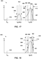
- FIG 17 is a graphical illustration 400 of a first spectrum 401 and a second spectrum 402, according to an embodiment.
- the first spectrum 401 represents a portion of the collected energy signals within the energy window 406 (e.g., ⁇ E Window ).
- the energy window 406 extends from lines 408 and 410.
- the first spectrum 401 may be a portion of the spectrum 301 ( Figure 15 ) within the energy window 406.
- the first spectrum 401 is based on the collected energy signal.
- the portions of the spectrum 301 outside the energy window 406 are cut-off and/or removed by the controller circuit 136 to form the first spectrum 401.
- the first spectrum 401 can have similar characteristics with the spectrum 301.
- the first spectrum 401 includes all the events of the spectrum 301 that are within the energy window 406.
- the first spectrum 401 may have a FWHM corresponding to the width 306 similar to and/or the same as the spectrum 301.
- the first spectrum 401 has the peak 308 at the energy level at E p (Q) similar to and/or the same as the spectrum 301.
- the events in the low energies tail 312 of the spectrum 301, which is outside the energy window 406 are corrected.
- the controller circuit 136 corrects the energies based on Equation 4, represented as ⁇ V.
- the ⁇ V represents the delta charge of the collected energy signal from the pixelated anode 116 and the sum of the adjacent energy signals from adjacent pixelated anodes 114 and 118.
- Equation 4 corrects the energies acquired by the pixelated anode 110, such as the pixelated anode 116, to be independent of a location (x, y, z) of the acquired events.
- the controller circuit 136 selects a portion of the collected energy signal and a portion of the adjacent energy signals that are outside the energy window 406.
- the controller circuit 136 selects a portion of the collected energy signals acquired by the pixelated anode 116 that are outside the energy window 406.
- the controller circuit 136 calculates a sum of the adjacent energy signals for the adjacent pixelated anodes 114, 118 that are outside the energy window 406.
- the controller circuit 136 multiplies the sum of the adjacent energy signals by the adjusting factor (e.g., C ), and subtracts the value from the collected energy signal of the pixelated anode 116 to determine ⁇ V.
- ⁇ V represents a voltage signal corresponding to the corrected energies of the energy tail 312 of the spectrum 301.
- ⁇ V represents a difference in the peak values 213 measured by the P&H circuit 200 ( Figure 6 ) of the electronic channels 111 between the pixelated anodes 114, 116, 118.
- the corrected energies are independent of the locations (x, y, z) of the events acquired by the pixelated anode 116.
- the values of the ⁇ V forms the second spectrum 402.
- the second spectrum 402 is similar to the spectrum 351 ( Figure 16 ), but includes less events.
- the spectrum 351 includes all of the events in the spectrum 301, and the second spectrum 402 includes the events that are outside of the energy window 406.
- the second spectrum 402 includes only the events that are outside of the energy window 406.
- a peak of the second spectrum 402 is different.
- the peak of the second spectrum 402 has a lower amplitude than the peak 352 of the spectrum 351.
- the peak of the second spectrum 402 is at the same position as the peak 352 of the spectrum 351.
- the second spectrum 402 has the same and/or similar width 358 (e.g., ⁇ E' 2 ) as the spectrum 351 between lines 354 and 356.
- the second spectrum 402 includes a low energy tail 404.
- the low energy tail 404 has a lower amplitude than the low energy tail 312 of the spectrum 301.
- the peak of the second spectrum 402 is positioned at an energy value of E p ( ⁇ Q 1 ).
- the controller circuit 136 shifts and/or combines the second spectrum 402 with the first spectrum 401.
- the second spectrum 402 is based on the corrected values of the ⁇ V.
- the peak of the second spectrum 402 is shifted such that it is aligned with the peak 308 of the spectrum 401.
- the controller circuit 136 shifts/stretches and/or combines the second spectrum 402 with the first spectrum 401.
- the shifting/stretching by the controller circuit 136 is done by multiplying the second spectrum 402 by the ratio (e.g., K ) as shown in Equation 6, which is equivalent to the charge ratio of peak 308 and peak 352.
- the controller circuit 136 determines the ratio based on the peak 308 of the spectrum 301 and the delta charge.
- the ratio is configured to adjust a gain and/or position of the peak of the second spectrum 402.
- the controller circuit 136 adjusts the second spectrum 402 by multiplying the second spectrum 402 by the ratio (e.g., K).
- the adjustment to the second spectrum 402 by the controller circuit 136 stretches and/or shifts the second spectrum 402. For example, the stretching and/or shifting of the second spectrum 402 by the ratio (e.g., K ) and combine with the first spectrum 401.
- the combination of the shifted/stretched second spectrum 402 and the first spectrum 401 forms a corrected energy spectrum 451 shown in Figure 18 , which has reduced low energies tail.
- Figure 18 is a graphical illustration 450 of an embodiment of the corrected energy spectrum 451.
- the corrected energy spectrum 451 represents a combination of the first and second spectrums 401, 402.
- the corrected energy spectrum 451 is corrected for a low energy tail for events outside the energy window 406 (e.g., between 408 and 410).
- the corrected energy spectrum 451 has a width 454 (e.g., ⁇ E 3 ) and the peak 308 representing the energy absorbed by the photons.
- the width 454 of the corrected energy spectrum 451 is wider than the width 306 of the spectrum 301 ( Figure 15 ).
- Equation 9 the relationship between the widths 306 (e.g., ⁇ E 1 ), 364 (e.g., ⁇ E 2 ), 454 (e.g., ⁇ E 3 ) are shown in Equation 9. ⁇ E 2 > ⁇ E 3 > ⁇ E 1
- the corrected energy spectrum 451 includes a low energy tail 452 outside the energy window 406. It may be noted that the low energy tail 452 is lower and/or reduced relative to the low energy tail 312.
- the low energy tail 312 of the spectrum 301 is produced mainly by the dependency on the DOI of the measured signals produced on the pixelated anodes 110, and by the charge sharing events. Typically, about 60% of the events of the spectrum 301 are within the energy window 406, 10% are charge sharing events, and 30% are events that depends on the DOI.
- the corrected spectrum 451 is the sum of the first and second spectrums 401, 402. The peaks of the first and second spectrums 401, 402 have differences in amplitudes at a ratio of 60/30, respectively.
- the corrected energy spectrum 451 is configured to have a higher energy resolution relative to the spectrum 353.
- the energy resolution is determined by the controller circuit 136 based on Equation 8. For example, the energy resolution of the corrected spectrum 353 is 9%.
- the energy resolution of the corrected spectrum 451 is 5.15% with a reduced low energy tail 452.
- Figure 19 is a graphical illustration 500 of an embodiment of Gaussian curves 502, 504, 506 representing spectra 401, 402 and the corrected energy spectrum 451 of Figures 17 and 18 , respectively.
- the graphical illustration 500 includes two Gaussian curves 502, 504 that are added together to produce the Gaussian curve 506.
- the Gaussian curves 502, 504 are represent the first and second spectrums 401, 402, respectively.
- the Gaussian curves 502, 504, 506 include widths 501, 503, 505.
- the widths 501, 503, 505 are related to each other by the ratio 4, 9, 5.15, respectively.
- the widths 501, 503, 505 are indicative of the widths 306, 358, 454 of the spectrums 401, 402, 451, respectively.
- the corrected spectrum 451 is the combination of the first and second spectrums 401, 402.
- the corrected spectrum 451 includes a reduced low energy tail 452 relative to the low energy tail 312 ( Figure 15 ).
- a reduction in the low energy tail 452 includes a minor degradation in the energy resolution from 4% to 5.15%.
- the low energy tails can be created by the charge sharing events.
- the charge sharing events correspond to an electrical charge of an event is spilt between two adjacent pixelated anodes 110.
- the electrical charge on the pixelated anodes 110 depend on the location of the event.
- a correction can be applied by the controller circuit 136 for the correction of the charge sharing event and the correction for the dependency of the measured signals in the pixelated anodes 110 on the DOI (e.g., location of the event).
- the controller circuit 136 is configured to distinguish between a charge sharing events and events that the charge induced depends on the DOI.
- a part of the electrical charge of the event is shared between two pixelated anodes 110.
- the controller circuit 136 determines the charge sharing event when the sum of the signals collected from two pixelated anodes 110 is within a predetermined range around the value of the electrical charge produced by absorption of a photon in the RPD 100.
- the controller circuit 136 identifies the events for the adjacent pixelated anodes 110 as the charge sharing event.
- the charge sharing event is counted by the controller circuit 136 as one event belonging to one of the adjacent pixelated anodes 110.
- the correction for charge sharing events by the controller circuit 136 to recover the electrical charge of the event is done by adding the signals from the two adjacent pixelated anodes 110 that the event is split. Additional discussion regarding sub-pixels may be found, for example, in U.S. Patent Application Serial No. 14/627,436 , entitled “Systems and Methods for Improving Energy Resolution by Sub-Pixel Energy Calibration," filed 20-February-2015, and U.S. Patent Application Serial No. 15/280,640 , entitled “Systems and Methods for Sub-Pixel Location Determination,” filed 29-September-2016, which are hereby incorporated by reference in their entirety.
- a width of a spectrum corrected for charge sharing events is wider than the width 306 of the spectrum 301.
- the width 306 of the spectrum 301 is derived from the measurement of the pixelated anode 116.
- the width of the charge sharing event is broadened by the noise of two adjacent pixelated anodes 110.
- the noise is generated by the RPD 100, the electronic channel 111 coupled to the adjacent pixels 110, and/or the like.
- a spectrum corrected for charge sharing events is determined by the controller circuit 136 by adding the events from the two adjacent anodes 110. Accordingly, the width of a spectrum corrected for charge sharing is calculated according to Equation 10.
- ⁇ ⁇ 2 ⁇ ⁇ E 1
- the variable ⁇ E 1 represents the width 306 of the spectrum 301.
- the broadening of the width 306 is represented by the factor of ⁇ 2 and stands only for the events corrected for charge sharing events. It may be noted that not all the events in the spectrum 301 are corrected for charge sharing events, the width 306 of spectrum 301 will be broaden by a factor that is smaller than ⁇ 2.
- the factor represents the noise of two pixelated anodes 110 (e.g., the pixelated anode 116, one of the adjacent pixelated anode 114, 118) of the RPD 100, the noise associated with the electronic channels 111, and/or the like.
- the noise associated with the spectrum of a charge sharing event corrected is higher than the noise associated with the spectrum 301.
- the events corrected for either charge sharing and/or dependency on the location of the events produces a wider spectrum.
- the wider spectrum degrades the energy resolution of the RPD 100.
- the controller circuit 136 is configured to reduce the overall degradation of the energy resolution. For example, by correcting the spectrum for events having energies that are outside the energy window (e.g., the energy window 406), which are in the range of the low energies tail to be corrected.
- the remaining events outside the energy window, which are not charge sharing events are identified by the controller circuit 136 as an event that the electrical charge depends on the DOI.
- the correction for the dependency of the events on the DOI was discussed above.
- Figure 20 is a flow chart of a method 600 for reducing a low energy tail in an energy spectrum.
- the method 600 may employ structures or aspects of various embodiments (e.g., systems and/or methods) discussed herein.
- certain steps (or operations) may be omitted or added, certain steps may be combined, certain steps may be performed simultaneously, certain steps may be performed concurrently, certain steps may be split into multiple steps, certain steps may be performed in a different order, or certain steps or series of steps may be re-performed in an iterative fashion.
- portions, aspects, and/or variations of the method 600 may be used as one or more algorithms to direct hardware to perform one or more operations described herein.
- the controller circuit 136 calibrates the RPD 100. For example, the calibration of the RPD 100 adjusts a gain and offset.
- the calibration by the controller circuit 136 includes measuring a spectrum of a collected energy signal for two known energies corresponding to two known isotopes. Based on the spectrum, the controller circuit 136 determines a calibrated spectrum for the collected energy signals.
- the controller circuit 136 may determine the adjusting factor (e.g., C ) for Equation 4.
- the adjusting factor defines the value of ⁇ V to not be zero when the collected energy signal 156 and the adjacent energy signal 252 correspond to a value subsequent to 258 along the horizontal axis of Figure 14 .
- the adjusting factor may be determined by the controller circuit 136 based on morphologies (e.g., slope, peaks, overall shape) of the adjacent energy signal 250 and the collected energy signal 156. For example, the controller circuit 136 may determine when the slopes of the collected energy signal 156 and the adjacent energy signal 250 are different and/or diverge during the calibration. The slopes of the collected and adjacent energy signals 156, 250 diverge at the distance 258 along the horizontal axis. Based on a position at the distance 258, the controller circuit 136 may determine the adjusting factor.
- morphologies e.g., slope, peaks, overall shape
- the controller circuit 136 measures a collected energy signal from a first pixelated anode 110, for at least one event. For example, for each event (e.g., the event 124, the second event 125, the third event 117) the controller circuit 136 measures the collected energy signal 156 ( Figure 14 ) from the pixelated anode 116 absorbing the photon 141.
- the controller circuit 136 measures an adjacent energy signal from at least two adjacent pixelated anodes 110, for at least one event.
- the at least two adjacent pixelated anodes 110 are aligned either along the X and/or Y-coordinate or on both sides of the first pixel and located symmetrically relative to the first pixelated anode.
- the event 124 ( Figure 3 ) is located within the pixelated anode 116.
- the at least two adjacent pixelated anodes 110 can include the pixelated anodes 114, 118 both along the X-coordinate and/or the pixelated anodes 120, 122 along the Y-coordinate relative to the pixelated anodes 116.
- the adjacent energy signal may include one or more of the pixelated anodes 114, 118, 120, 121, 122, 123, 127, 129 as described in Equation 4a.
- the adjacent energy signal represents the induced charge on the at least two adjacent pixelated anodes as the negative charge cloud traverses to the pixelated anode 116.
- the controller circuit determines if the least one event is the charge sharing event.
- the controller circuit 136 can determine a charge sharing event by comparing the collected energy signal (e.g., of the pixelated anode 116) with the adjacent energy signal (e.g., of the pixelated anode 114, 118, 120, 122) during the at least one event.
- the event is located at the line 144 ( Figure 4 ) the collected energy signal and the adjacent energy signal for both of the adjacent pixelated anodes are similar and/or the same within a predetermine non-zero threshold.
- the at least one event is located at the line 144.
- the controller circuit 136 measures the collected energy signal of the pixelated anode 116 and the adjacent energy signal of the pixelated anode 118.
- the controller circuit 136 may compare the collected energy signal and the adjacent energy signal. If a difference between the collected energy signal and the adjacent energy signal is within a predetermine non-zero threshold, the controller circuit 136 may determine that the event corresponds to a charge sharing event.
- the charge sharing event positioned on the line 144 may be a specific example, the general criteria to distinguish between charge sharing event and induced adjacent signals can be based on the Equation 3. For example, the sum of the adjacent signals from the adjacent pixelated anodes located symmetrically on both side of the pixelated anode having the event is equal to 2V 0 . Accordingly, for events when the sum is not equal to 2V 0 , the controller circuit 136 may determine the event is a charge sharing event.
- the controller circuit 136 performs a charge sharing correction.
- the controller circuit 136 adjusts the collected energy signal to include a portion of the adjacent energy signal representing a charge sharing pixelated anode.
- the charge sharing event is located at the line 144 ( Figure 4 ).
- the electrical charge of the charge sharing event is split between the pixelated anodes 116 and the pixelated anode 118 (e.g., the charge sharing pixelated anode).
- the collected energy signal measured at the pixelated anode 116 is adjusted based on the portion of the adjacent energy signal of the pixelated anode 118. For example, a charge of the collected energy signal is increases to include the charge of the adjacent energy signal for the charge sharing event.
- the controller circuit 136 produces and/or generates a charge sharing spectrum.
- the controller circuit 136 produces a spectrum of the number of charge sharing event versus the energy of the events corrected for charge sharing.
- the spectrum may have a peak energy at E p (Q) as shown in Figures 15-18 .
- the controller circuit 136 determines if the at least one event is not within the energy window 406. For example, if the controller circuit 136 compares the electrical charge of the collected energy signal of the pixelated anode 116. If the electrical charge is outside the energy window 406 (e.g., below the line 408), the controller circuit 136 determines that the event is not within the energy window 406.
- the controller circuit 136 determines the first spectrum 401 ( Figure 17 ).
- the first spectrum 401 represents a number of events (e.g., along the vertical axis) versus the energy of the events (e.g., along horizontal axis).
- the first spectrum 401 includes the peak 308 at the energy value of E p (Q).
- the controller circuit 136 determines a delta charge based on the collected energy signal and the adjacent energy signal outside the energy window 406. For example, the controller circuit 136 subtracts the electrical charge of the collected energy signal as described in Equation 4. The controller circuit 136 sums the electrical charge of the adjacent energy values of the at least two adjacent pixelated anodes. The controller circuit 136 multiplies the sum by the adjusting factor (e.g., C ), and subtracts from the collected energy signal.
- the adjusting factor e.g., C
- the controller circuit 136 generates the second spectrum 402 ( Figure 17 ).
- the second spectrum 402 represents a number of event (e.g., along the vertical axis) versus the corresponding event energies (e.g., along the horizontal axis).
- the event energies are based on a portion of the collected and adjacent energy signals outside the event window 406.
- the controller circuit 136 stretches the second spectrum 402 based on the ratio (e.g., K). For example, the controller circuit 136 multiplies the second spectrum 402 by the ratio determined in Equation 6. The ratio is determined by the controller circuit 136 based on the peak 308 of the first spectrum 401, and the peak 352 (e.g., at E p ( ⁇ Q 1 )) of the second spectrum 402 (e.g., represents the delta charge). The stretching of the second spectrum 402 shifts or moves the peak 352 of the second spectrum 402 to the peak 308 (e.g., E p (Q)).
- the ratio e.g., K
- the ratio is determined by the controller circuit 136 based on the peak 308 of the first spectrum 401, and the peak 352 (e.g., at E p ( ⁇ Q 1 )) of the second spectrum 402 (e.g., represents the delta charge).
- the stretching of the second spectrum 402 shifts or moves the peak 352 of the second spectrum 402 to the
- the controller circuit 136 combines the second spectrum 402 with the charge sharing spectrum to form a unified second spectrum.
- the unified second spectrum includes the number of events of the charge sharing spectrum and the second spectrum 402.
- the controller circuit 136 combines the unified second spectrum with the first spectrum 401. For example, the controller circuit 136 combines the number of events of the unified second spectrum with the first spectrum 401.
- the unified second spectrum includes the corrected energies of the events having charge sharing events and/or that are dependent on a location of the at least one event (e.g., dependent on the DOI).
- the combination of the unified second spectrum and the first spectrum 401 produces a corrected energy spectrum (e.g., the corrected energy spectrum 451 of Figure 18 ).
- Figure 21 is a schematic block diagram of an embodiment of a medical imaging system 2100, in accordance with an embodiment.
- the medical imaging system 2100 is shown as a nuclear medicine (NM) imaging system.
- the medical imaging system 2100 may be a PET, SPECT, MBI, and/or the like.
- the medical imaging system 2100 includes a plurality of imaging detectors 2102 mounted to a gantry 2104.
- the imaging detectors 2102 are configured as two separate detector arrays 2106 and 2108 coupled to the gantry 2104 above and below a subject 2110 (e.g., a patient).
- the detector arrays 2106 and 108 may be coupled directly to the gantry 2104, or may be coupled via support members 2112 to the gantry 2104 to allow movement of the entire arrays 2106 and/or 2108 relative to the gantry 2104 (e.g., translating movement in the left or right direction as viewed in Figure 21 ).
- each of the imaging detectors 2102 includes a detector unit 2114 mounted to a movable detector carrier 2116 (e.g., a support arm or actuator that may be driven by a motor to cause movement thereof) that extends from the gantry 2104.
- the detector carriers 2116 allow movement of the detector units 2114 towards and away from the subject 2110, such as linearly and in parallel to each other.
- the imaging detectors 2102 may include one or more detector units 2114 coupled to a respective detector carrier 2116 and having dimensions of 4 cm to 20 cm and may be formed of tiles and/or modules of Cadmium Zinc Telluride (CZT), CdMnTe (CMT), Hgl, Si, GaAr, Si, Ge and/or the like.
- the gantry 2104 may be formed with an aperture 2118 (e.g., opening or bore) therethrough as illustrated.
- a patient table 2120 is configured with a support mechanism (not shown) to support and carry the subject 2110 in one or more of a plurality of viewing positions within the aperture 2118 and relative to the imaging detectors 2102.
- the gantry 2104 may also be configured in other shapes (e.g., "C", "H” and “L”), and may be rotatable about the subject 2110.
- Each of the imaging detectors 2102 have a radiation pixelated detector, which is directed towards the subject 2110 or a region of interest within the subject.
- the radiation pixelated detector may include one or more collimators 2122.
- the field of view for each of the imaging detectors 2102 may be increased, decreased, or relatively unchanged by the type of collimator 2122.
- the collimator 2122 is a multi-bore collimator, such as a parallel hole collimator.
- other types of collimators such as converging or diverging collimators may optionally or alternatively be used.
- collimator 2122 examples include pinhole, parallel-beam converging, diverging fan-beam, converging or diverging cone-beam, multi-bore converging, multi-bore converging fan-beam, multi-bore converging cone-beam, multi-bore diverging, or other types of collimator. In some embodiments, at least two types of collimators are used. Optionally, multi-bore collimators may be constructed to be registered with pixels of the detector units 2114.
- the medical imaging system 2100 includes a controller unit 2130.
- the controller unit 2130 is configured to control a movement and positioning of the patient table 2120, the imaging detectors 2102, the gantry 2104, the collimators 2122, and/or the like. A range of motion before or during an acquisition, or between different image acquisitions, is set to maintain the actual field of view (FOV) of each of the imaging detectors 2102.
- the controller unit 2130 may include a gantry motor controller, a table controller, a detector controller, a pivot controller, a collimator controller, and/or the like.
- the controllers may be automatically commanded by a controller circuit 2136, manually controlled by an operator, or a combination thereof.
- the imaging detectors 2102 may be positioned to image a portion of the subject 2110 based on events detected the controller circuit 2136. Positioning may be accomplished manually by the operator and/or automatically. After the imaging detectors 2102, gantry 2104, patient table 2120, and/or collimators 2122 are positioned by the controller unit 2130, one or more images are acquired by one or more of the imaging detectors 2102 being used. The image data acquired by the imaging detectors 2102 may be combined and reconstructed into a composite image, which may comprise two-dimensional (2D) images, a three-dimensional (3D) volume or a 3D volume over time (4D).
- a readout unit 2160 receives electrical signal data produced by the imaging detectors 2102 and converts this data into digital signals for subsequent processing.
- the readout unit 2160 may be similar to and/or the same as the readout unit 132 in Figure 5 . Additionally or alternatively, digital signals are generated by the imaging detectors 2102.
- An image reconstruction device 2162 and a memory 2164 may be provided in addition to the controller circuit 2136.
- the controller circuit 2136 is configured to control the operation of the medical imaging system 2100.
- the controller circuit 2136 may be similar to and/or the same as the controller circuit 136 in Figure 5 .
- the controller circuit 2136 may include one or more processors.
- the controller circuit 2136 may include a central processing unit (CPU), one or more microprocessors, or any other electronic component capable of processing input data according to specific logical instructions.
- the controller circuit 2136 may include and/or represent one or more hardware circuits or circuitry that include, are connected with, or that both include and are connected with one or more processors, controllers, and/or other hardware logic-based devices.
- the controller circuit 2136 may execute instructions stored on a tangible and non-transitory computer readable medium (e.g., the memory 2164).
- the readout unit 2160 and the image reconstruction device 2162 may be integrated with and/or a part of the controller circuit 2136.
- a user input device 2166 may be provided to receive user inputs (e.g., control commands), as well as a display 2168 for displaying images.
- the various embodiments may be implemented in hardware, software or a combination thereof.
- the various embodiments and/or components also may be implemented as part of one or more computers or processors.
- the computer or processor may include a computing device, an input device, a display unit and an interface, for example, for accessing the Internet.
- the computer or processor may include a microprocessor.
- the microprocessor may be connected to a communication bus.
- the computer or processor may also include a memory.
- the memory may include Random Access Memory (RAM) and Read Only Memory (ROM).
- the computer or processor further may include a storage device, which may be a hard disk drive or a removable storage drive such as a solid-state drive, optical disk drive, and the like.
- the storage device may also be other similar means for loading computer programs or other instructions into the computer or processor.
- the term "computer,” “subsystem,” “controller circuit,” “circuit,” or “module” may include any processor-based or microprocessor-based system including systems using microcontrollers, reduced instruction set computers (RISC), ASICs, logic circuits, and any other circuit or processor capable of executing the functions described herein.
- RISC reduced instruction set computers
- ASIC application-specific integrated circuit
- the computer, subsystem, controller circuit, circuit, or module execute a set of instructions that are stored in one or more storage elements, in order to process input data.
- the storage elements may also store data or other information as desired or needed.
- the storage element may be in the form of an information source or a physical memory element within a processing machine.
- the set of instructions may include various commands that instruct the computer, subsystem, controller circuit, and/or circuit to perform specific operations such as the methods and processes of the various embodiments.
- the set of instructions may be in the form of a software program.
- the software may be in various forms such as system software or application software and which may be embodied as a tangible and non-transitory computer readable medium. Further, the software may be in the form of a collection of separate programs or modules, a program module within a larger program or a portion of a program module.
- the software also may include modular programming in the form of object-oriented programming.
- the processing of input data by the processing machine may be in response to operator commands, or in response to results of previous processing, or in response to a request made by another processing machine.
- a structure, limitation, or element that is “configured to” perform a task or operation is particularly structurally formed, constructed, or adapted in a manner corresponding to the task or operation.
- an object that is merely capable of being modified to perform the task or operation is not “configured to” perform the task or operation as used herein.
- the use of "configured to” as used herein denotes structural adaptations or characteristics, and denotes structural requirements of any structure, limitation, or element that is described as being “configured to” perform the task or operation.
- a controller circuit, circuit, processor, or computer that is "configured to" perform a task or operation may be understood as being particularly structured to perform the task or operation (e.g., having one or more programs or instructions stored thereon or used in conjunction therewith tailored or intended to perform the task or operation, and/or having an arrangement of processing circuitry tailored or intended to perform the task or operation).
- a general purpose computer which may become “configured to” perform the task or operation if appropriately programmed) is not “configured to” perform a task or operation unless or until specifically programmed or structurally modified to perform the task or operation.
- the terms "software” and “firmware” are interchangeable, and include any computer program stored in memory for execution by a computer, including RAM memory, ROM memory, EPROM memory, EEPROM memory, and nonvolatile RAM (NVRAM) memory.
- RAM memory random access memory
- ROM memory read-only memory
- EPROM memory erasable programmable read-only memory
- EEPROM memory electrically erasable programmable read-only memory
- NVRAM nonvolatile RAM
Landscapes
- Physics & Mathematics (AREA)
- Spectroscopy & Molecular Physics (AREA)
- Health & Medical Sciences (AREA)
- Life Sciences & Earth Sciences (AREA)
- General Physics & Mathematics (AREA)
- High Energy & Nuclear Physics (AREA)
- Molecular Biology (AREA)
- Measurement Of Radiation (AREA)
Abstract
Description
- The subject matter disclosed herein relates generally to imaging systems, and more particularly to methods and systems for reducing low-energy tails of a radiation detector.
- Conventional radiation detectors receive one or more photons during an imaging session. The absorption of a photon represent an event that is collected by the radiation detector. When the radiation detector absorbs the photon a negative charge cloud of electrons and a positive charge cloud of holes are created. The negative charge cloud of electrons drifts toward the positively charged anode of the conventional radiation detector. The positive charge cloud of holes drifts toward the negatively charged cathodes of the radiation detector. The positive charge cloud moves slower relative to the negative charge cloud.
- For any single event, the photon may be absorbed at various depths within the radiation detector. The depth is between the cathode or anode and a location where the photon, which is absorbed and referred to as a depth of interaction (DOI). A charge induced by the positive charge cloud on the cathode is negligible in some semiconductors, such as CdZnTe (CZT), which have low value of the product µτ for holes. The variable µ represents mobility, and the variable τ is the electron lifetime. The charge on the anode is proportional to the depth of a location of the event where the photon is absorbed.
- The charge is associated with events, and are collected and recorded as corresponding energy values. During an imaging session of the radiation detector, multiple events are tracked and the corresponding energy values are recorded. The energy values for the events are analyzed to form one or more energy spectrums. The energy spectrums represent a count of a number of events at corresponding energy values of a select range (e.g., a histogram). The energy spectrum may be divided into a primary energy range and a low energy tail. The primary energy range is positioned to include a peak in the energy spectrum, while the low energy tail includes energy levels below the peak. The low energy tail reduces the efficiency of the radiation detector.
- To reduce the low energy tail, conventional methods utilize: i) small anodes combined with a steering grid for creating a small pixel effect; ii) a co-planar grid including two interleaved grids that are biased by two different potentials to create a collecting and non-collecting grids (e.g., Luke grid); or iii) a small pixel effect combined with a signal derived from the cathode to calculate the DOI for applying electronic corrections. However, the conventional method of using the small anodes combined with the steering grid requires the use of many electronic channels. Conventionally, one electronic channel is coupled to each anode of the radiation detector. Accordingly, the use of small anodes requires the use of many anodes and electronic channels, which is a technical challenge. Additionally, the anodes require high voltage bias that is different from the high voltage bias applied to the steering grid, and the steering grid complicates the integration of the detector components due to interconnections and packaging.
- Additionally, the conventional method of using the co-planar grid (e.g., the Luke grid) includes two high density grids interleaved together. The high density of the grids are necessary to create a similar response regardless of a location of the event. Accordingly, the conventional method is not useful for imaging purposes as it does not provide information on the event location. Further, the co-planar grid utilizes a permanent analog subtraction between the signals of the collecting and non-collecting grids for all of the events. The permanent analog subtraction decreases the signal-to-noise ratio for all of the events including events that do not need to be corrected by the co-planar grid. Additionally, the co-planar grid cannot be implemented with pixelated anodes as the co-planar grid requires a permanent analog differential subtraction between the pairs of pixels.
- In accordance with an embodiment, a method (e.g., for reducing a low energy tail in an energy spectrum) is provided. The method includes measuring a collected energy signal from a first pixel of a radiation pixelated detector during at least one event, and measuring adjacent energy signals from at least two pixels adjacent to the first pixel of the radiation pixelated detector during the at least one event. The method includes generating a first spectrum based on the collected energy signal of the at least one event within an energy window. The energy window being a predetermined energy range for medical imaging. The method includes determining a delta charge based on the collected energy signal and the adjacent energy signals generated during the at least one event,
- In accordance with an embodiment, a system (e.g., a medical imaging system) is provided. The system includes a radiation pixelated detector having a plurality of pixelated anodes operably coupled to corresponding electronic channels. The system includes a controller circuit. The controller circuit is operably coupled to the electronic channels. The controller circuit is configured to measure a collected energy signal from a first pixel of the radiation pixelated detector during at least one event, and measure an adjacent energy signals from at least two second pixels adjacent to the first pixel of the radiation pixelated detector during the at least one event. The controller circuit is configured to generate a first spectrum based on a portion of the collected energy signal of the at least one event within an energy window. The energy window being a predetermined energy range for medical imaging. The controller circuit is configured to determine a delta charge based on the collected energy signal and the adjacent energy signals generated during the at least one event, generate a second spectrum based on the delta charge of the at least one event outside the event window, and stretching the second spectrum to combine with the first spectrum to form a corrected energy spectrum based on the delta charge.
- In accordance with an embodiment, a method (e.g., for reducing a low energy tail in an energy spectrum) is provided. The method includes measuring a collected energy signal from a first pixel of a radiation pixelated detector during at least one event, measuring adjacent energy signals from at least two pixels adjacent to the first pixel of the radiation pixelated detector during at least one event, and determining a corrected energy signal based on the collected energy signal and the adjacent energy signals based on an adjusting factor. The method includes determining a delta charge based on the collected energy signal and the adjacent energy signals, generating a spectrum based on the delta charge of the at least one event, and stretching the spectrum to form a corrected energy spectrum based on the delta charge.
- In the drawings:
-
Figure 1 is a side view of an embodiment of a portion of a radiation pixelated detector. -
Figure 2 is a peripheral view of an embodiment of a portion of a radiation pixelated detector. -
Figure 3 is an expanded portion the radiation pixelated detector shown inFigure 2 . -
Figure 4 is a side view of the expanded portion shown inFigure 3 . -
Figure 5 is a schematic illustration of an embodiment of a radiation pixelated detector having electronic channels operably coupled to a controller circuit. -
Figure 6 is a schematic illustration of an embodiment of operations performed by the electronic channels shown inFigure 4 , -
Figure 7 is a graphical illustration of a charge of a pixelated anode based on a distance traversed by a negative charge cloud. -
Figure 8 is a graphical illustration of an embodiment of collected energy signals and adjacent energy signals. -
Figure 9 is a graphical illustration of an embodiment of a collected energy signal and an adjacent energy signal. -
Figure 10 is a graphical illustration of an embodiment of an adjacent energy signal. -
Figure 11 is a graphical illustration of an embodiment of an adjacent energy signal. -
Figure 12 is a graphical illustration of an embodiment of an adjacent energy signal. -
Figure 13 is a graphical illustration of an embodiment of an adjacent energy signal. -
Figure 14 is a graphical illustration of an embodiment of a collected energy signal and a sum of adjacent energy signals. -
Figure 14A is a graphical illustration of a delta charge waveform based on the collected energy signal and the sum of adjacent energy signals shown inFigure 14 . -
Figure 15 is a graphical illustration of an embodiment of a spectrum. -
Figure 16 a graphical illustration of an embodiment of a spectrum and a corrected energy spectrum. -
Figure 17 is a graphical illustration of an embodiment of a first and second spectrum. -
Figure 18 is a graphical illustration of an embodiment of a corrected energy spectrum. -
Figure 19 is a graphical illustration of an embodiment of Gaussian curves representing a corrected energy spectrum. -
Figure 20 is a flow chart of a method for reducing a low energy tail in an energy spectrum. -
Figure 21 is a schematic block diagram of an embodiment of a medical imaging system. - The following detailed description of certain embodiments will be better understood when read in conjunction with the appended drawings. To the extent that the figures illustrate diagrams of the functional modules of various embodiments, the functional blocks are not necessarily indicative of the division between hardware circuitry. Thus, for example, one or more of the functional blocks (e.g., processors or memories) may be implemented in a single piece of hardware (e.g., a general purpose signal processor or a block of random access memory, hard disk, or the like). Similarly, the programs may be stand-alone programs, may be incorporated as subroutines in an operating system, may be functions in an installed software package, and the like. It should be understood that the various embodiments are not limited to the arrangements and instrumentality shown in the drawings.
- As used herein, an element or step recited in the singular and proceeded with the word "a" or "an" should be understood as not excluding plural of said elements or steps, unless such exclusion is explicitly stated. Furthermore, references to "one embodiment" of the present invention are not intended to be interpreted as excluding the existence of additional embodiments that also incorporate the recited features. Moreover, unless explicitly stated to the contrary, embodiments "comprising" or "having" an element or a plurality of elements having a particular property may include additional elements not having that property.
- Generally, various embodiments provided herein describe radiation pixelated detectors for ionizing radiation, such as X-Ray and Gamma-Rays, and more specifically for radiation detectors of a medical imaging system such as a nuclear imaging system, a gamma camera, Single Photon Emission Computed Tomography (SPECT), Molecular Brest Imaging (MBI), Positron Emission Tomography (PET), and/or the like. The medical imaging systems described herein are configured to be insensitive to the DOI. The medical imaging system reduces the low energy tail of the radiation pixelated detector of a spectrum of collected energy signals during at least one event.
- A technical effect provided by at least one embodiment includes providing a pixelated radiation detector that is insensitive to the DOI and is able to provide location information for an event. A technical effect provided by at least one embodiment includes providing a pixelated radiation detector that is insensitive to the DOI and has pixelated anodes that are biased to a common potential. A technical effect provided by at least one embodiment includes providing a pixelated radiation detector that is insensitive to the DOI. A technical effect provided by at least one embodiment includes applying a correction method only to the events that need to be corrected for the DOI.
- An "energy spectrum" or "spectrum" can refer to a histogram of a number of events grouped into corresponding energy values measured by the medical imaging system during an imaging session. The energy values represent a measured charge for a select event. The energy spectrum includes a number of events having the corresponding energy values. For example, the energy spectrum can be shown graphically as the number of events versus the measured energy values.
- An "energy window" is a predetermined range of energy values of the energy spectrum for medical imaging that may include the spectrum peak. The predetermined range of energy values can correspond to anatomical structures within a patient.
- A "low energy tail" can refer to a range of energy values of the energy spectrum remote from a peak of the energy spectrum and/or outside the energy window. The low energy tail is formed mainly from the dependency of the energy value (e.g., charge) on a location of the DOI of where the photon is absorbed within a pixelated radiation detector.
- A "solid viewing angle" can refer to an orientation and/or angle of a location of an event and/or a negative charge cloud relative to a pixelated anode. The solid viewing angle is independent along X and Y-coordinates of the pixelated anode having the event. For example, the solid viewing angle of different (x, y) locations of events and/or the negative charge cloud within the pixelated anode can have similar and/or the same solid viewing angles with respect to each other.
-
Figures 1 and2 illustrate a portion of a radiation pixelated detector (RPD) 100, in accordance with an embodiment.Figure 1 illustrates a side view of theRPD 100, andFigure 2 illustrates a peripheral view of theRPD 100. TheRPD 100 includes asemiconductor plate 102. Thesemiconductor plate 102 may include CZT, CMT, Hgl, Si, GaAr, Si, Ge, and/or the like. Thesemiconductor plate 102 includes first andsecond surfaces monolithic cathode contact 108 is overlaid on thesecond surface 106 of thesemiconductor plate 102. Thecathode 108 of theRPD 100 is biased by a negative high-voltage (e.g., "-HV").Pixelated anodes 110, representing a plurality of pixels of theRPD 100, are overlaid on thefirst surface 104. Thepixelated anodes 110 are shown having square shapes with dimensions of "W x W" and a pitch "P." Additionally or alternatively, thepixelated anodes 110 may be a circle, a triangle, a rectangle, and/or the like. TheRPD 100 has a thickness "D" based on thesemiconductor plate 102, which is designed to absorb radiation that includes photons (e.g., thephotons 141 can be grouped into a plurality of photons 140) having energy within the range of ionizing radiation (e.g., X-Ray and/or Gamma Ray radiation). - An event occurs when a
photon 141 interacts with theRPD 100, and thephoton 141 is absorbed by thesemiconductor 102. The absorbedphoton 141 generates an electrical charge signal on one or more of thepixelated anodes 110, which is proportional to the energy of the absorbedphoton 141. Apixelated anode 110 is operably coupled to a correspondingelectronic channels 111. Additionally or alternatively, theelectronic channels 111 may be operably coupled to more than onepixelated anode 110. - The
electronic channels 111 are configured to process the electrical charge signal from thepixelated anodes 110 and form a voltage signal. Theelectronic channels 111 include charge sensitive preamplifiers (CSP) 109. TheCSP 109 are configured to clamp the potential of thepixelated anodes 110 to a voltage that is equal to the voltage of a virtual ground of theCSP 109. For example, theCSP 109 clamps the voltage of thepixelated anodes 110 to a potential at and/or approximate to zero. -
Figure 3 is an expandedportion 100A of theRPD 100 shown inFigure 2 , in accordance with an embodiment. The expanded portion is represented by aframe 112 shown inFigure 2 . TheRPD 100 is shown aligned with an X, Y, Z Cartesian coordinatesystem 126. The expandedportion 100A includes the pixelated anodes 110 (e.g., thepixelated anodes pixelated anodes system 126. Thepixelated anodes system 126. The expandedportion 100A includessidewalls 101 of thesemiconductor plate 102. Thesidewalls 101 have a thickness D, which is aligned along the Z-coordinate between the first andsecond surfaces - The expanded
portion 100A of theRPD 100 includes anevent 124. Thephoton 141 is absorbed by thepixelated anode 116 creating theevent 124. Thepixelated anodes pixelated anode 116. For example, thepixelated anodes pixelated anode 116 along the X-coordinate. Theevent 124 is located at a coordinate of (x1, y, z) within thepixelated anode 116. The coordinates are determined relative to an origin position based on thepixelated anode 110, which absorbs thephoton 141. For example, the coordinate of theevent 124 is based on a position relative to thepixelated anode 116. The values along the X and Y-coordinates are measured relative to an origin at a center of thepixelated anode 116. The value along the Z-coordinate is measured relative to thesecond surface 106. For example, the zero value of the z coordinate is located on the intersection point between the Z-coordinate and thesecond surface 106. - The point where the
photon 141 is absorbed (e.g., the event 124) produces negative and positive charge clouds. Thepixelated anode 116 collects electrons within the negative charge cloud to form the collected energy signal. For example, the negative charge cloud drifts towards thepixelated anode 116 based on the high voltage bias between thecathode 108 and thepixelated anode 116. Thepixelated anodes pixelated anode 116, generate an adjacent energy signal. The adjacent energy signal is produced by the induction of the electrical charge signal as the negative charge cloud drifts towards thepixelated anode 116. - As described herein, the collected energy signal weakly depends and/or is independent on a location of the
event 124 along the X and Y-coordinates of thepixelated anode 116. The adjacent energy signal depends on the location of theevent 124 along the X and Y-coordinates of thepixelated anode 116. It may be noted as described herein a sum of the adjacent energy signals from adjacent pixels located symmetrically on both sides of the collecting pixel. For example, thepixelated anodes pixelated anode 116, which is the location of theevent 124. By summing the adjacent energy signals, the location of the event weakly depends and/or is independent on the location of theevent 124 along the X and Y coordinates of thepixelated anode 116. The collected energy signal and the adjacent energy signal depend on the location of theevent 124 along the Z-coordinate. For example, the location of theevent 124 along the Z-coordinate corresponds to the DOI of theevent 124. -
Figure 4 is a side view of the expandedportion 100A, in accordance with an embodiment. The side view represents a cross-section along the line A-A' shown inFigure 3 . Theevent 124 is located at a coordinate (x1, y, z). The y coordinate is not specified. The collected energy signal and the adjacent energy signal are independent of the location of theevent 124 along the Y-coordinate. The X coordinate is measured relative to the center of thepixelated anode 116. The location of theevent 124 being at thesecond surface 106 corresponds to a z coordinate of zero. - The point where the
photon 141 is absorbed (e.g., at the event 124) produces the negative and positive charge clouds. The negative and positive charge clouds correspond to electrical charges -q and +q, respectively. The electrical charge signal of the negative and positive charge clouds are proportional to the energy of thephoton 141 absorbed by thepixelated anode 116. The collected energy signal of thepixelated anode 116 and the adjacent energy signal of thepixelated anodes pixelated anodes 110 and the drift of the positive charge cloud toward thecathode 108. The amount of the electrical charge signal that the positive and negative charge clouds contribute (e.g., by induction) to the collected and adjacent energy signals are proportional to a length of the distance that the charge clouds travel toward thepixelated anode 110 and thecathode 108, respectively. It may be noted that the potential of thepixelated anodes 110 and thecathode 108 is based on the -HV bias supplied to thecathode 108. - Optionally, a type of the
semiconductor plate 102 may affect a rate of drift of the positive and negative charge clouds. For example, thesemiconductor plate 102 can include CZT, which reduces a mobility of the positive charge cloud relative to the negative charge cloud. Optionally, the positive charge cloud may be static. Accordingly, the positive charge cloud may not contribute to the electrical charge signal of the collected and adjacent energy signals. For example, the collected and adjacent energy signals may be based only on the negative electron cloud. - Additionally or alternatively, the -HV bias on the
cathode 106 may be configured to generate an electrical field within thesemiconductor plate 102 to be free of electron traps. The -HV bias allows the negative charge cloud to drift along adrift path 145 from thecathode 108 to thepixelated anode 116 along a distance "D" enabling a complete charge collection. The complete charge collection occurs when all of the electrons of the negative charge cloud is absorbed by thepixelated anode 110. For example, a rate that the negative charge cloud drifts along thedrift path 145 to thepixelated anode 116 is shorter than an electron lifetime τ of the electrons of the negative charge cloud. Based on the rate, all of the electrons are absorbed by thepixelated anode 116, which represents the complete charge collection. - The complete charge collection of the collected energy signal is equal to the induced charge of the electron in the negative charge cloud generated by the
event 124. Additionally, the complete charge collection is proportional to the distance "D" traversed by the negative charge cloud along thedrift path 145 of the negative charge cloud. Concurrently as the negative charge cloud traverses along thedrift path 145, an electrical charge is induced on thepixelated anodes pixelated anodes pixelated anodes event 124 relative to thepixelated anode 116 is more proximate relative to thepixelated anodes pixelated anodes event 124 compared to thepixelated anode 116. - It may be noted that for large pixels, as shown in
Figure 7 the collectedenergy signal 154, both the collected and adjacent energy signals of theevent 124 are proportional to the distance "D" that the negative charge cloud traverses along thedrift path 145. Each of thepixelated anodes event 124. For example, a solid viewing angle of thepixelated anodes pixelated anode 116. The viewing angles of thepixelated anode 116 are dependent on a value of a Z-coordinate and weakly dependent along the X and Y-coordinates of theevent 124. As the negative charge cloud drifts toward thepixelated anode 116 the Z-coordinate change. The solid viewing angle of the Z-coordinates to collectinganode 116 is weakly dependent and/or independent on the location ofevent 124 along the X and Y coordinates. For the same value of coordinate Z mentioned above, the solid viewing angles from theevent 124 to adjacentnon-collecting anodes event 124 along the X-coordinate but, are weakly dependent and/or independent on the Y-coordinate of theevent 124. Accordingly, the solid viewing angles of thepixelated anodes event 124 along the Y-coordinate. The solid viewing angle of thepixelated anodes pixelated anodes 110 of theRPD 100 is proportional to an integral along coordinate Z, in a range starting from the location of theevent 124 and ending at the correspondingpixelated anode 110. The integral is calculated over the solid viewing angles as a function of the Z-coordinates along the trajectory of the negative charge cloud to the correspondingpixelated anode 110. - For example, the location of the
event 124 in thepixelated anode 116. The electrical charge induced on thepixelated anodes 116 represents the integral from the location whereevent 124 was created (e.g., located at the absorption location of photon 141) and ends at thepixelated anode 116 along the Z-coordinates. In this range of Z-coordinates, the integral is performed over the viewing angles from theevent 124 to thepixelated anode 116 as a function of Z (e.g., DOI) along thedrift path 147 of the negative charge cloud. The collected energy signal induced on thepixelated anode 116 is independent on the location ofevent 124 along the X-Y plane and the adjacent energy signals induced on the adjacentpixelated anodes event 124 along the X-coordinate, but are independent on the Y-coordinate. - In connection with the
event 124 shown inFigure 4 , the difference in the solid viewing angles results in magnitudes of the adjacent energy signals induced on thepixelated anodes pixelated anode 116. The adjacent energy signal of thepixelated anodes Equations 

- The variable V118 of
Equation 1 represents the adjacent energy signal of thepixelated anode 118 as a function of a value of the X-coordinate measured from the center of thepixelated anode 116. The variable V114 ofEquation 2 represents the adjacent energy signal of thepixelated anode 114 as a function of a value of the X-coordinate measured from the center ofpixelated anode 116. The constant V0 represents a value of the induced electrical charge measured at thepixelated anodes event 124 drift is at point x=0 and y=0 at the center ofpixel 116. The constant α represents the linearity coefficient of theRPD 100. The adjacent energy signals defined inEquations pixelated anodes event 124 along the X-coordinate. The sum of the adjacent energy signals of thepixelated anodes Equation 3, results in a sum of the adjacent energy signals, which is independent along the X-coordinate.
pixelated anode 116 and the sum of the adjacent energy signals from thepixelated anodes event 124 along the X and Y-coordinates, but depend on the location along the Z-coordinate. The dependency of the collected energy signal on the location of theevent 124 along the Z-coordinate, representing the DOI, is undesired and produces the low energy tail. For example, the low energy tail is produced when photons having the same energy produce different induced charges on the collected energy signal based on the DOI. The low energy tail is measured by theRPD 100 at different energies and appear as a tail in an energy spectrum that is remote from a peak of the energy spectrum. - For events located within the
pixelated anode 116, a difference between the collected energy signal and the sum of the adjacent energy signals (e.g., measures by the adjacentpixelated anodes 114, 118) is represented as the variable ΔV, in Equation 4. As described herein, the difference between the collected energy signal and the sum of the adjacent energy signals can be used to reduce the low energy tail.
- The variable V116 of Equation 4 represents the collected energy signal, and the variables V114 and V118 represents the adjacent energy signals of the
pixelated anodes - When the difference (e.g., ΔV) is zero, the photons for a plurality of events along a range are absorbed by the
RPD 100. The range is along the Z-coordinate. The range represents where the photons are absorbed in theRPD 100 above thecathode 108. For example, the range represents when the sum of the solid viewing angles of the adjacentpixelated anodes pixel 116. Within the range, the absorption of the photons are distant relative to thepixelated anodes pixelated anode 116 that is approximately equal to the sum of the solid viewing angles ofpixelated anodes pixelated anodes pixelated anodes - The expanded
portion 100A ofFigure 3 includes asecond event 125. Thesecond event 125 is at a location having coordinates (P/2-Δx, y, z). The y coordinate is not specified. The collected energy signal and the adjacent energy signal are independent of the location of thesecond event 125 along the Y-coordinate. The X-coordinate is measured relative to the center of thepixelated anode 116. The location of thesecond event 125 being at thesecond surface 106 corresponds to a Z-coordinate of zero. - The
line 144 is a symmetry line between thepixelated anodes pixelated anodes line 144 is located at a distance P/2 from the center of thepixelated anode 116. When a photon is absorbed at theline 144 or at a distance fromline 144 that is smaller than the diameter of the electrons cloud, the resulting event represent a charge sharing event. The negative charge cloud resulting from the absorbed photon (e.g., the event) is divided between the two adjacentpixelated anodes pixelated anode 116. In another example, a portion of the negative charge cloud positioned on a right side of the line 144 (e.g., positioned within the pixelated anode 118) is drifted toward thepixelated anode 118. Based on the partition of the negative charge cloud, the charge induced by the negative charge cloud on thepixelated anode pixelated anodes pixelated anodes - For additional discussion regarding charge sharing events and sub-pixel location determinations are described in
U.S. Patent Application Serial No. 14/627,436 U.S. Patent Application Serial No. 14/724,022 U.S. Patent Application Serial No. 15/280,640 - The location of the
second event 125 is removed from theline 144 by a distance of Δx. The distance is larger than a diameter of the negative charge cloud, and does not represent the charge sharing event. For example, the electrons of the negative charge cloud is not shared between the adjacentpixelated anodes second event 125 traverses along adrift path 147. Thedrift path 147 extends a distance "D" between the first andsecond surfaces pixelated anode 116. For example, thepixelated anode 116 has the complete charge collection for thesecond event 125. Concurrently, thesecond event 125 induces a charge on the adjacentpixelated anodes second event 125 is more proximate to thepixelated anode 118 relative to thepixelated anode 114. For example, the solid viewing angles of thepixelated anodes second event 125 to thepixelated anode 118, the induced charge on thepixelated anode 118 is greater than thepixelated anode 114. - The expanded
portion 100A includes athird event 117. Thethird event 117 is at a location having coordinates (P/2-Δx, y, zi). The Y-coordinate is not specified. The collected energy signal and the adjacent energy signal are independent of the location of thethird event 117 along the Y-coordinate. The X-coordinate is measured relative to the center of thepixelated anode 116. The location of thethird event 117 is at a positon Z=1 along the Z-coordinate. - The negative charge cloud formed by the
third event 117 drifts towards thepixelated anode 116. Similar to thesecond event 125, the negative charge cloud of thethird event 117 drifts along thedrift path 147. However, the locations representing the DOI of the second andthird events events third event 117 drifts a shorter distance along thedrift path 147 relative to the negative charge cloud of thesecond event 125. Based on the difference in positions along the Z-coordinate, the charges on thepixelated anodes pixelated anode 116 and the induced charge on thepixelated anodes third event 117 relative to thesecond event 125. - A charge of the negative charge clouds of the second and
third events third events pixelated anodes events pixelated anode 116 between the second andthird events RPD 100. - As described herein, the difference between the collected energy signal and the sum of the adjacent energy signals can be used, which is independent on the locations (e.g., independent of the DOI) of the events (e.g., the
event 124, thesecond event 125, the third event 117). For example, the difference can be used as a signal of events to produce a spectrum of theRPD 100 to reduce low energy tails. -
Figure 5 is aschematic illustration 220 of an embodiment of theRPD 100 having theelectronic channels 111 operably coupled to acontroller circuit 136, in accordance with an embodiment. Theschematic illustration 220 includes areadout unit 132 and amemory 138. Theelectronic channel 111 may include one or more processors. Optionally, theelectronic channels 111 may include a central processing unit (CPU), one or more microprocessors, or any other electronic component capable of processing input data according to specific logical instructions. Optionally, theelectronic channels 111 may include and/or represent one or more hardware circuits (e.g., analog components) or circuitry that include, are connected with, or that both include and are connected with one or more processors, controllers, and/or other hardware logic-based devices. Additionally or alternatively, theelectronic channels 111 may execute instructions stored on a tangible and non-transitory computer readable medium. - The
pixelated anodes 110 of theRPD 100 are electrically and/or operably coupled to theelectronic channels 111 viainterconnections 131. Theinterconnections 131 are configured to clamp a voltage potential of thepixelated anodes 110 to be equal to a virtual ground (e.g., approximately zero) of charge sensitive pre-amplifiers (CSP) 109, shown inFigure 6 . Theelectronic channels 111 receive the electrical charge signals measured by thepixelated anodes 110 via theinterconnections 131. - The
electronic channels 111 are electrically and/or operably coupled to thereadout unit 132. Thereadout unit 132 is configured to collect the voltage signals received from theelectronic channels 111, and to convert the analog values of the voltage signals into digital values. For example, thereadout unit 132 may include analog to digital converters. Optionally, thereadout unit 132 may be integrated with theelectronic channels 111 and/or thecontroller circuit 136. Thereadout unit 132 is configured to generate a digital addresses associated with each of the digital values. The digital address corresponds to one of thepixelated anodes 110 that generated an electrical charge signal in response to the event. Thereadout unit 132 is configured to generate adata packet 146 representative of the voltage signals. Thedata packet 146 may include aheader 143 containing an address representing a location of thepixelated anode 110 on theRPD 100. Thedata packet 146 includes apayload 149. Thepayload 149 includes the digital values generated by thereadout unit 132 representative of the voltage signal produced by thepixelated anode 110. - The
data packets 146 are transmitted from thereadout unit 132 via aport 134 to thecontroller circuit 136 and stored in thememory 138. Thecontroller circuit 136 may include a central processing unit (CPU), one or more microprocessors, or any other electronic component capable of processing input data according to specific logical instructions. Optionally, thecontroller circuit 136 may include and/or represent one or more hardware circuits or circuitry that include, are connected with, or that both include and are connected with one or more processors, controllers, and/or other hardware logic-based devices. Additionally or alternatively, thecontroller circuit 136 may execute instructions stored on a tangible and non-transitory computer readable medium (e.g., the memory 138). - The
data packets 146 in thememory 138 are analyzed by thecontroller circuit 136. For example, thecontroller circuit 136 is configured to execute one or more models and/or algorithms stored in thememory 138 that may include, charge-sharing correction, low-energy tail correction, image reconstruction, and/or the like as described herein to process the digital values and generate the image data. -
Figure 6 is a schematic illustration of the operations performed by theelectronic channels 111, in accordance with an embodiment. Theelectronic channels 111 is shown performing a plurality of operations shown as theCSP 109, ashaper circuit 135,thresholding circuit 137,amplifier circuit 139, and a peak and hold (P&H)circuit 200 to process the electrical charge signals received from theinterconnections 131. The operations may correspond to operations performed by one or more processors by theelectronic channels 111 and/or be configured hardware (e.g., ADC converters, amplifiers, filters) of theelectronic channels 111. - The
CSP 109 is configured to integrate the electrical charge signal from thepixelated anodes 110. Anintegrated signal 203 is representative of an integrated electrical charge signal by theCSP 109. The electrical charge signal is integrated overtime 201 by theCSP 109 to define theintegrated signal 203. Based on the integration of the electrical charge signal, theintegrated signal 203 reaches asteady state value 202. Thesteady state value 202 represents the total induced charge collected by thepixelated anodes 110. The lowest potential of thepixelated anode 110, for example, is determined by theCSP 109, which is configured to clamp the potential of thepixelated anodes 110 to a voltage that is equal and/or similar to the voltage of the virtual ground of theCSP 109. - The
integrated signal 203 is passed to theshaper circuit 135. Theshaper circuit 135 is configured to filter the integrated signal 203 (e.g., band-pass filter) to increase a signal to noise ratio of theintegrated signal 203. For example, the filtering by theshaper circuit 135, changes theintegrated signal 203 to form a filtered signal 205 (e.g., a Gaussian shape having an amplitude 204). - The filtered
signal 205 is passed to thethreshold circuit 137. Thethreshold circuit 137 is configured to pass theamplitude 204 of the filteredsignal 205 to theamplifier circuit 139 when theamplitude 204 is above a predetermined non-zero threshold, or to block theamplitude 204 when theamplitude 204 is below the predetermined non-zero threshold. Anamplitude 206 of athresholded signal 207 may be equal to or larger than theamplitude 204 of the filteredsignal 205, which depends on the amplification of thethreshold circuit 137. Thethresholded signal 207 is passed to theamplifier circuit 139. Theamplifier circuit 139 is configured to amplify thethresholded signal 207 by increasing theamplitude 206. For example, theamplifier circuit 139 increases theamplitude 206 of thethresholded signal 207 to form an amplifiedsignal 209 having an increasedamplitude 208. - The amplified
signal 209 is passed to theP&H circuit 200. TheP&H circuit 200 is configured to amplify the amplifiedsignal 209 to hold a maximum value of the amplifiedsignal 209 corresponding to and/or about theamplitude 208 to form thevoltage signal 211. Thevoltage signal 211 includes a risingportion 215 and apeak value 213. The peak value may be similar to and/or about theamplitude 208. Thevoltage signal 211 is received by thereadout unit 132. - The
payload 149 of thedata packet 146 includes digital values of thepeak value 213 of thevoltage signal 211, which is stored later in thememory 138. Optionally, thepayload 149 may include theamplitudes signals peak value 213 of thepixelated anodes 110 is a representation of the electrical charge of the photon absorbed by theRPD 100. -
Figure 7 is agraphical illustration 150 of an induced charge on the collectingpixelated anode 116 based on a distance traversed by a negative charge cloud, in accordance with an embodiment. The distance traversed by the negative charge cloud along thedrift path 145 is along the Z-coordinate from thecathode 108 to thepixelated anode 116. A direction of the drift is shown as a direction of anarrow 152. The negative charge cloud is formed by the absorption of thephoton 141 in thepixelated anode 116. - The charge on the collecting
pixelated anode 116 is independent on the location of theevent 124 along the X and Y-coordinates. The independency of the charge is based on the solid viewing angles. Different (x, y) locations of events within thepixelated anode 116 have similar viewing angles to thepixelated anode 116 from the different locations of theevents pixelated anode 116. Based on the independency relative to the X and Y-coordinates, the location of theevent 124 at (x, y) of thepixelated anode 116 are not shown in thegraphical representation 150. - A
line 160 indicates the location of theevent 124 along the Z-coordinate. For example, theline 160 is positioned at thecathode 108 representing a coordinate z = 0. Aline 157 indicates a location of thepixelated anode 116. For example, theline 157 has a position along the Z-coordinate of z = "D," which is a thickness of thesemiconductor 102. -
Collected energy signals pixelated anode 116 based on a distance the negative charge cloud drifts from thecathode 108 thepixelated anode 116. The collectedenergy signals pixelated anode 116 having different dimensions of thepixelated anode 116. The collectedenergy signals pixelated anode 116 having different dimensions WxW relative to the thickness "D" of thesemiconductor 102. - The
pixelated anode 116 of the collectedenergy signal 154 has dimensions WxW that are larger than the thickness "D" of theRPD 100. For example in the collectedenergy signal 154, an aspect ratio of the dimensions W/D is greater than one. The charge of the collectedenergy signal 154 is shown increasing linearly as the negative charge cloud traverses to thepixelated anode 116. - The
pixelated anode 116 of the collectedenergy signal 156 has dimensions WxW representing an aspect ratio W/D that is equal to 0.5. The charge of the collectedenergy signal 156 is shown increasing non-linearly as the negative charge cloud traverses to thepixelated anode 116. - The
pixelated anode 116 of the collectedenergy signal 158 has dimensions WxW that are less than the thickness "D" of theRPD 100. For example, a ratio of the dimensions WxW representing aspect ratio W/D that is less than 0.5. The charge of the collectedenergy signal 158 is shown increasing exponentially as the negative charge cloud traverses to thepixelated anode 116. -
Figures 8 and 9 aregraphical illustrations energy signals adjacent energy signals energy signals pixelated anode 116. Theadjacent energy signals pixelated anode 118, which is adjacent to thepixelated anode 116. The collectedenergy signals adjacent energy signals pixelated anodes energy signals adjacent energy signals pixelated anodes arrow 152. Thepixelated anodes graphical illustrations pixelated anodes pixelated anode 116 of the collectedenergy signal 156 inFigure 7 . - The collected
energy signal 156 is based on thesecond event 125. For example, the negative charge cloud is formed at the location (e.g., P/2-Δx, y, z) of thesecond event 125. The collectedenergy signal 156 starts atpoint 181 proximate to thecathode 108 of theRPD 100, which represents a coordinate of z = 0. The charge of the collectedenergy signal 156 increases as the negative charge cloud traverses towards thepixelated anode 116. The collectedenergy signal 156 ends atpoint 185 representing a position of thepixelated anodes points RPD 100. The collectedenergy signal 156 reaches a peak 193 at thepoint 185. - Similarly, the
adjacent energy signal 166 is based on thesecond event 125. Theadjacent energy signal 166 starts at thepoint 181 and ends at thepoint 185. Theadjacent energy signal 166 represents the induced charge on thepixelated anode 118 based as the negative charge cloud drifts to thepixelated anode 116. The induced charge on thepixelated anode 118 increases as the negative charge cloud traverses from thecathode 108 to thepixelated anode 116. For example, as the negative charge cloud traverses along thedrift path 147, the solid viewing angle increases with respect to thepixelated anode 118. - At a
point 199 along the Z-coordinate, the solid viewing angle of thepixelated anode 118 decreases. For example, as the negative charge cloud traverses to the pixelated anode 116 a distance between the negative charge cloud and thepixelated anode 118 changes. Between thepoints pixelated anode 116. The distance between the negative charge cloud and thepixelated anode 118 decreases. Based on the decrease in distance, the induced charge on thepixelated anode 118 increases reaching apeak 191. Subsequent to thepoint 199 as the negative charge cloud drifts to thepixelated anode 116, the distance between the negative charge cloud and thepixelated anode 118 increases. The increase in the distance, further decreases the solid viewing angle of thepixelated anode 118. The decrease in the solid viewing angle decreases the induced charge on thepixelated anode 118. For example, the charge induced on thepixelated anode 118 has a different polarity or negative charge. The change in polarity of the charge induced on thepixelated anode 118 occurs at thepoint 199. Based on the changes in polarity of the induced charge, thepeak 191 is formed by theadjacent energy signal 166. As the negative charge cloud traverses to thepixelated anode 116, theadjacent energy signal 166 continues to decrease to a charge of zero at thepoint 185. In the range between thepoint 181, where z = 0, to thepoint 199, bothenergy signals - The
peaks adjacent energy signals peak value 213 determined by the P&H circuit 200 (Figure 6 ) in the correspondingelectronic channels 111. For example, the digital values (e.g., within the payload 149) of the peaks 193,191 correspond to thepeak value 213 stored in thememory 138 with corresponding addresses (e.g., within the header 143) representing thepixelated anodes - The collected energy signal 186 (
Figure 9 ) represents the charge (e.g., Q shown along the vertical axis) measured at thepixelated anode 116. The collectedenergy signal 156 is based on thethird event 117. For example, the negative charge cloud is formed at the location (e.g., P/2-Δx, y, z = 1) of thethird event 117. The collectedenergy signal 186 starts atpoint 183, which represents a coordinate of z = 1. The charge of the collectedenergy signal 186 increases as the negative charge cloud traverses towards thepixelated anode 116. Similar to theadjacent energy signal 156, the polarity of the induced charge changes at thepoint 199. The collectedenergy signal 186 ends atpoint 185 representing a position of thepixelated anodes energy signal 186 reaches a peak 195 at thepoint 185. - The collected
energy signals pixelated anode 116. For example, the collectedenergy signal 186 has a smaller electrical charge relative to the collectedenergy signal 156. The difference in electrical charges is based on the distance traversed by the negative charge clouds of thesecond event 125 and thethird event 117, respectively. For example, the location of thethird event 117 is at z = 1 or thepoint 183. The location of thesecond event 125 is at z = 0 or thepoint 181. The negative charge cloud of thesecond event 125 traverses the thickness D of theRPD 100 to thepixelated anode 116. The negative charge cloud of thethird event 117 traverses from thepoint 183 to thepixelated anode 116. The distance traversed by the negative charge cloud of thethird event 117 is less than the distance traversed by the negative charge cloud of thesecond event 125. As describe herein, the charge on thepixelated anode 116 increases based on the distance traversed by the negative charge cloud along the Z-coordinate. Based on the difference in the distances, thepeak 193 is higher relative to thepeaks 195. - Similarly, the
adjacent energy signal 188 is based on thethird event 117. Theadjacent energy signal 188 starts at thepoint 183 and ends at thepoint 185. Theadjacent energy signal 188 represents the induced charge on thepixelated anode 118 based on the negative charge cloud formed at the location of thethird event 117. The induced charge on thepixelated anode 118 increases as the negative charge cloud traverses to thepixelated anode 116. For example, as the negative charge cloud traverses along thedrift path 147, the solid viewing angle increases with respect to thepixelated anode 118. - Based on the shorter distance traversed by the negative charge cloud of the
third event 117, theadjacent energy signal 188 ends at 185 with a negative charge. Between thepoints third event 117 traverses to thepixelated anode 116, the charge induced on thepixelated anode 118 increases. Theadjacent energy signal 188 reaches apeak 197. At thepoint 199, the solid viewing angle decreases and the distance of the negative charge cloud to thepixelated anode 118 increases. Based on the reduction in the solid viewing angle, the charge induced on theadjacent energy signal 188 decreases. For example, the charge induced on thepixelated anode 118 changes polarity and is negative. As the induced charge continues to decrease, theadjacent energy signal 188 ends at a negative charge at thepoint 185. - The difference in distances traversed by the negative charge clouds of the second and
third events peaks peak 197 is smaller than thepeak 191. A range of theadjacent energy signals point 185 of theadjacent energy signal 166 is equal to a range of charge between the peak 197 and thepoint 185 of theadjacent energy signal 188. An amount of negative charge induced on thepixelated anode 118, represented in the ranges, on theadjacent energy signals - Additionally or alternatively, for different event locations the adjacent energy signals may or may not end with a negative induced charge at the
point 185. For example, the adjacent energy signals end at a negative charge at thepoint 185 when the location of the events have a coordinate x close to P/2 and z = 1 (e.g., the third event 117). - The
peaks adjacent energy signals peak value 213 determined by the P&H circuit 200 (Figure 6 ) in the correspondingelectronic channels 111. For example, the digital values (e.g., within the payload 149) of thepeaks peak value 213 stored in thememory 138 with corresponding addresses (e.g., within the header 143) representing thepixelated anodes - A difference between the
peaks adjacent energy signals delta charge 189 between thepeaks adjacent energy signals delta charge 189 corresponds to thesecond event 125 located on and/or proximate to the cathode 108 (e.g., at z = 0). In another example, thedelta charge 187 between thepeaks adjacent energy signals delta charge 189 corresponds to thethird event 117 located at thepoint 183. - The delta charges 187, 189 are based on
different events adjacent energy signals events adjacent energy signals -
Figure 8 and 9 correspond to theevents events pixelated anode 118 and remote from thepixelated anode 114 along the X-coordinate. For example, the proximity of theevents pixelated anode 118 represent a maximum and/or large charge induced on thepixelated anode 118 for theadjacent energy signals pixelated anode 114 is minimal and/or small. According toEquation 3, the sum of the adjacent energy signals from thepixelated anodes events pixelated anodes pixelated anode 118 alone. Additionally or alternatively, theadjacent energy signal pixelated anode 118 for theevents pixelated anodes events pixelated anode 116 and the sum of the adjacent energy signals of thepixelated anodes 114, 118 (e.g., based on Equation 4). Thereby the delta charges 187, 189 are independent of the locations of theevents - The collected and
adjacent energy signals point 181 to thepoint 199. The collected andadjacent energy signals point 183 to thepoint 199. For example, the differences between the collected andadjacent energy signals points points - The charge deltas 187, 189 can be calculated based on integrals of the collected
energy signals charge delta 187 for thethird event 117 is equal to an integral along the Z-coordinate of the collectedenergy signal 186 between thepoints charge delta 189 for thesecond event 125 is equal to an integral along the Z-coordinate of the collectedenergy signal 156 between thepoints energy signals energy signals events energy signals events - The difference between the collected and
adjacent energy signals points points point 199, the difference of the collected andadjacent energy signals -
Figures 10-14 are graphical representations of the collected and adjacent energy signals measured at thepixelated anodes Figures 10-13 illustrate changes in the induced charge on the adjacentpixelated anodes pixelated anodes RPD 100. For example, the aspect ratio of D/W is 0.5. -
Figure 10 is agraphical representation 1000 of theadjacent energy signal 166, in accordance with an embodiment. Theadjacent energy signal 166 is similar to and/or the same as theadjacent energy signal 166 shown inFigure 8 . Theadjacent energy signal 166 represents the induced charge on thepixelated anode 118. Theadjacent energy signal 166 is based on the second event 125 (Figure 4 ). For example, theadjacent energy signal 166 represents the induced charge as the negative charge cloud traverses along thedrift path 147 to thepixelated anode 116 from thecathode 108. Theadjacent energy signal 166 extends along the horizontal axis in the direction of thearrow 152 representing the movement of the negative charge cloud. Theadjacent energy signal 166 extends from a zero coordinate representing the location of thesecond event 125 to the width "D" of theRPD 100 along the Z-coordinate. -
Figure 11 is agraphical representation 1100 of theadjacent energy signal 250, in accordance with an embodiment. Theadjacent energy signal 250 represents the induced charge on thepixelated anode 114. Theadjacent energy signal 250 is based on the second event 125 (Figure 4 ). For example, theadjacent energy signal 250 represents the induced charge as the negative charge cloud traverses along thedrift path 147 to thepixelated anode 116 from thecathode 108. Theadjacent energy signal 250 extends along the horizontal axis in the direction of thearrow 152 representing the movement of the negative charge cloud. Theadjacent energy signal 250 extends from a zero coordinate representing the location of thesecond event 125 to the width "D" of theRPD 100 along the Z-coordinate. - The location of the
second event 125 is positioned proximate to thepixelated anode 118. For example, the location of thesecond event 125 along the X-coordinate relative to the center ofpixelated anode 116 is at P/2-Δx. The location of thesecond event 125 along the X-coordinate relative to the center ofpixelated anode 116 is at - (P/2-Δx). Thesecond event 125 is located a distance of Δx from thepixelated anode 118, which is remote from thepixelated anode 114 at a distance of P-Δx. Based on the difference in location of thesecond event 125 relative to thepixelated anodes adjacent energy signal 166 received from thepixelated anode 118 is greater than the induced charge on theadjacent energy signal 250 received from thepixelated anode 114. -
Figure 12 is agraphical representation 1200 of theadjacent energy signal 1202, in accordance with an embodiment. Theadjacent energy signal 1202 represents the induced charge on thepixelated anode 118. Theadjacent energy signal 1202 is based on the event 124 (Figure 4 ). For example, theadjacent energy signal 1202 represents the induced charge as the negative charge cloud traverses along thedrift path 145 to thepixelated anode 116 from thecathode 108. Theadjacent energy signal 1202 extends along the horizontal axis in the direction of thearrow 152 representing the movement of the negative charge cloud. Theadjacent energy signal 1202 extends from a zero coordinate representing the location of theevent 124 to the width "D" of theRPD 100 along the Z-coordinate -
Figure 13 is agraphical representation 1300 of theadjacent energy signal 1302, in accordance with an embodiment. Theadjacent energy signal 1302 represents the induced charge on thepixelated anode 114. Theadjacent energy signal 1302 is based on the event 124 (Figure 4 ). For example, theadjacent energy signal 1302 represents the induced charge as the negative charge cloud traverses along thedrift path 145 to thepixelated anode 116 from thecathode 108. Theadjacent energy signal 1302 extends along the horizontal axis in the direction of thearrow 152 representing the movement of the negative charge cloud. Theadjacent energy signal 1302 extends from a zero coordinate representing the location of theevent 124 to the width "D" of theRPD 100 along the Z-coordinate - The location of the
event 124 is positioned along the X-coordinate relative to the center ofpixelated anode 116 at X=x1. The location of theevent 124 along the X-coordinate relative to the center ofpixelated anode 116 is at -x1. For example, theevent 124 is located a distance of x1 from thepixelated anode 118, and a distance of - x1 from thepixelated anode 114. When the value of x1 is zero, the induced charges on theadjacent energy signals -
Figure 14 is agraphical representation 1400 ofadjacent energy signals 252 and the collectedenergy signal 156, in accordance with an embodiment. The collectedenergy signal 156 is similar to and/or the same as the collectedenergy signal 156 shown inFigures 7-8 . Theadjacent energy signals 252 is a sum of theadjacent energy signals Equation 3, a sum of theadjacent energy signals events adjacent energy signals events - As described herein, the collected and
adjacent energy signals events adjacent energy signals Figure 14 . Adelta charge 1402 is shown between thepeak 193 of the collectedenergy signal 156 and apeak 1404 of the adjacent energy signals 252. As described herein, thedelta charge 1402 is independent along the X, Y, and Z-coordinates. - At
point 256, represented as at aline 254 along the horizontal axis, a morphology of the collected andadjacent energy signals adjacent energy signals distance 258 along the Z-coordinate. When the negative charge cloud traverses between thecathode 108 and thedistance 258, the electrical charge on thepixelated anode 116 is the same and/or similar value as the sum of theadjacent energy signals 252 of thepixelated anodes energy signal 156 and theadjacent energy signals 256 is zero. After the negative charge cloud reaches thedistance 258, the morphology of the collected andadjacent energy signals energy signal 156 increases. Alternatively, the induced charge of theadjacent energy signals 252 decreases and/or changes polarity. -
Figure 14A is agraphical illustration 260 of a delta charge (e.g., ΔQ1)waveform 262. Thedelta charge waveform 262 represents a difference between the collectedenergy signal 156 and the adjacent energy signals 252. Thedelta charge waveform 262 is divided into tworanges cathode 108. Therange 266 extends along the horizontal axis from thecathode 108 to thedistance 258. As shown inFigure 14 , the collected andadjacent energy signals cathode 108 to thedistance 258. During therange 266, the collected andadjacent energy signals - The
range 264 extends along the horizontal axis from thedistance 258 to thepixelated anodes Figure 14 , the morphologies of the collected andadjacent energy signals distance 258 along the horizontal axis. Based on the change in morphologies, thedelta charge waveform 262 increases exponentially and/or rapidly in the direction of thearrow 152. As indicated by thedelta charge waveform 262, the negative charge cloud contributes to the delta charge after traversing thedistance 258. The negative charge cloud continually contributes to the delta charge until reaching thepixelated anode 116 at the distance "D" along the Z-coordinate. For example, the photons corresponding to theevents range 266, by thepixelated anodes events - The viewing angle of the
pixelated anodes event 124 weakly depends on the values of the Y-coordinates. Further to reduce the dependency of the viewing angle, on Y-coordinate of theevent 124 can be achieved by including additional adjacent pixelated anodes. For example, the sum of the adjacent energy signals may be acquired by summing the adjacent energy signals from all or part of the adjacentpixelated anodes Figure 3 ) that are adjacent to thepixelated anode 116 that includes theevent 124. The sum may be determined by thecontroller circuit 136 as a linear combination of the adjacent energy signals from thepixelated anodes pixelated anode 116. - The sum of the linear combination as mentioned above is less dependent on the X and Y-coordinates of the
event 124 within thepixelated anode 116. Additionally or alternatively, a sum of the viewing angles of thepixelated anodes event 124 is independent on the location (x, y) of theevent 124. Based on the additional adjacentpixelated anodes 
- The variable C is the adjusting factor as described in Equation 4. The variables V114, V118, V120, V121, V122, V123, V127, V129 represent the adjacent energy signals measured by the
pixelated anodes pixelated anode 116. The variables k114, k118, k120, k121, k122, k123, k127, k129 represent factors configured to adjust the adjacent energy signals of thepixelated anodes RPD 100. For a certain range of Z-coordinates of theevent 124 in thepixelated anode 116, the value of the difference ΔV given by Equation 4a above may be equal to and/or be adjusted to be equal to zero based on the values of the adjusting factor (e.g., C) and the factors (e.g., k114, k118, k120, k121, k122, k123, k127, k129 ). For a range of the Z-coordinates of theevent 124 located in thepixelated anode 116, the collected energy signal (e.g., V116) and the adjusted sum of thepixelated anodes RPD 100. When the difference is equal to zero (e.g., ΔV = 0) in the range along Z-coordinates, the collected energy signal and the adjusted sum of the adjacent energy signals are the same for all the events within thepixelated anode 116. Thereby, all the events within thepixelated anode 116 will produce the same signal ΔV regardless on the location of the event along coordinates (x, y, z). - In reference to
Figures 15-19 , since the delta charge is independent of the coordinates (x, y, z) of the event, thecontroller circuit 136 utilizes the delta charge to reduce the low energy tail of a spectrum.Figures 15- 18 are graphical representations of spectrums of measured electrical charges. The spectrums are based onRPD 100 that have been calibrated for gain and offsets using measurements by two isotopes. -
Figure 15 is agraphical illustration 300 of aspectrum 301, in accordance with an embodiment. Thespectrum 301 is based on a number of events (e.g., theevents pixelated anodes 110, such as thepixelated anode 116, of theRPD 100. The number of events is shown along the vertical axis. An energy for the number of events is shown along the horizontal axis. For example, thespectrum 301 may represent a combination of collected energy signals for at least one event. Thespectrum 301 is not corrected for charge sharing events and/or correction of the low energies tail. - For example, the
spectrum 301 may be based on a number of events acquired by thepixelated anode 116. Thespectrum 301 includes a peak 308 positioned at an energy value of Ep(Q). Thepeak 308 represents an energy level for a largest number of events measured by thecontroller circuit 136. Thespectrum 301 includes alow energy tail 312 extending from 310 to an energy at 314. The value of thespectrum 301 at 310 may be based on the predetermined non-zero threshold of thethreshold circuit 137. For example, the value of thespectrum 301 at 310 may correspond to charges measured by thecontroller circuit 136 that are above the predetermined non-zero threshold. The low energy tail is formed by the different locations of the at least one events (e.g., DOI) within thepixelated anode 116. - The
spectrum 301 includes a width 306 (e.g., ΔE1) extending from the energies at 302 to 304 representing a full-width-half-maximum (FWHM) of thespectrum 301. Thewidth 306 may be defined at half of a height of a number of events of thepeak 308. For example, the width correspond to half of the number of events of thepeak 308. Thewidth 306 may be formed by an electrical noise, which affects the charge measured during the at least one event of the first pixel. The electrical noise may be generated by theRPD 100, theelectronic channels 111, and/or the like. -
Figure 16 is agraphical illustration 350 of an embodiment of aspectrum 351 and a correctedenergy spectrum 353. Thespectrum 351 is based on collected and adjacent energy signals for a plurality of events. Thespectrum 351 represents a number of events (plotted along the vertical axis) versus corrected energies along the horizontal axis. The energies of thespectrum 351 are corrected based on Equation 4, represented as ΔV. The ΔV represents the delta charge of the collected and adjacent energy signals. Equation 4 corrects the energies acquired by thepixelated anodes - For example, the collected energy signals are acquired by the
pixelated anode 116. Thecontroller circuit 136 calculates a sum of the adjacent energy signals for the adjacentpixelated anodes controller circuit 136 multiplies the sum of the adjacent energy signals by the adjusting factor (e.g., C), and subtracts the value from the collected energy signal of thepixelated anode 116 to determine ΔV. ΔV represents a voltage signal corresponding to the corrected energies of thespectrum 351. For example, ΔV represents a difference in the signals measured by the P&H circuit 200 (Figure 6 ) of theelectronic channels 111 between the collected energy signal of thepixelated anode 116 and the sum of the adjacent energy signals of thepixelated anodes spectrum 351 is independent of the locations (x, y, z) of the events acquired by thepixelated anode 116. - The
spectrum 351 is independent on the location of the events along the Z-coordinate (e.g., DOI) and along the X and Y-coordinates. Based on the corrected energy of thespectrum 351, thespectrum 351 includes a reducedlow energy tail 366. Thelow energy tail 366 is smaller relative to thelow energy tail 312 ofFigure 15 . For example, thelow energy tail 366 ranges from 310 to aline 354 of thespectrum 351. The corrected energies of thespectrum 351 include values of the adjacent energy signals (e.g., induced charge measured at thepixelated anodes 114, 118). For example, the threshold circuit 137 (Figure 6 ) of theelectronic channel 111 is configured to have a pre-determined non-zero threshold that allows the induced charge measured by thepixelated anodes - The
spectrum 351 includes apeak 352. Thepeak 352 corresponds to a corrected energy having a largest number of events. Thepeak 352 represents the delta charge (e.g., ΔQ) between thepeak value 213 of the collected and adjacent energy signals outputted by theP&H circuit 200 of electronic channels 111 (Figure 5 ). Thespectrum 351 has a width 358 (e.g., ΔE'2) from theenergies 370 to 372. Thewidth 358 represents a FWHM of thespectrum 351. Thewidth 358 is produced by the noise of theRPD 100, the noise of theelectronic channel 111, and/or the like. Thewidth 358 is wider than thewidth 306 of thespectrum 301. For example, thespectrum 351 is based on more than onepixelated anode width 358 is based on an amount of noise provided by each of thepixelated anodes spectrum 351 is based on threepixelated anodes pixelated anode 116 of thespectrum 301. Accordingly, the noise associated with thespectrum 351 is represented as a factor equal to √3 as provided in Equation 5.
- The variable ΔE'2 represents the
width 358 of thespectrum 351. The variable AE1 represents thewidth 306 of thespectrum 301. Thewidth 306 is multiplied by a square root of a number ofpixelated anodes 110 of thespectrum 351. For example, thespectrum 351 is based on three pixelated anodes, thepixelated anodes - The
peak 352 of thespectrum 351 is positioned at an energy value of Ep(ΔQ1). Thepeak 352 should be shift and/or calibrated to show the real energy, for example at the energy value Ep(Q) of thepeak 308. As described herein, thespectrum 351 is based on a calibration, which offsets the energy value. Thepeak 352 is shifted such that the calibration is equal to zero. Thecontroller circuit 136 shifts thepeak 352 of thespectrum 351 to a corrected energy. The shifting by thecontroller circuit 136 is done by multiplying thespectrum 351 by a factor K as shown in Equation 6.
- The coefficient K represents a ratio. The
controller circuit 136 determines the ratio based on thepeak 308 of thespectrum 301 and thepeak 352 of the delta-charge spectrum 351. The ratio is configured to adjust a gain and/or position of thepeak 352 of thespectrum 351. The ratio, shown as the coefficient K, is determined based on Equation 6. The variable Q represents thepeak 308 of thespectrum 301. For example, Q represents the correct energy of the absorbed photons. The variable ΔQ represents the delta charge associated with thepeak 352 of thespectrum 351. Optionally, the value of the ratio may be adjusted according to the adjustment for the adjustment factor (e.g., C) - The
controller circuit 136 adjusts thespectrum 351 by multiplying thespectrum 351 by the ratio (e.g., K) to form the correctedspectrum 353. The adjustment to thespectrum 351 by thecontroller circuit 136 stretches and/or shifts thespectrum 351. For example, stretching and/or shifting thespectrum 351 by the ratio (e.g., K) to have the correctedspectrum 353 at thepeak 308. The adjustment to thespectrum 351 further stretches thewidth 358 to a width 364 (e.g., ΔE2) by the ratio. The correctedenergy spectrum 353 has awidth 364 between points 374 and 376 (e.g., betweenlines 360 and 362), which is at half of the height of thepeak 308. Thewidth 364 of the correctedenergy spectrum 353 is wider than thespectrum 351. Thewidth 364 of the correctedspectrum 353 is determined by thecontroller circuit 136 based onEquation 7.
- The corrected
energy spectrum 353 includes alow energy tail 368. Thelow energy tail 368 is formed by the stretching of thelow energy tail 366 of thespectrum 351. Based on the stretching of thelow energy tail 366 by the ratio, thelow energy tail 368 is wider than thelow energy tail 366. It may be noted that thelow energy tail 366 is lower than thelow energy tail 312 of the spectrum 301 (Figure 15 ). - Optionally, the
controller circuit 136 may calculate an energy resolution. The energy resolution (e.g., ER) represented as a percentage determined based on Equation 8.
- The variable ΔE represents the
width 306, 364 (e.g., FWHM) of the spectrum. The value EP represents thepeak 308. For example, the energy resolution of the spectrum 301 (Figure 15 ) is 4%. In another example, the ratio (e.g., K) is determined by thecontroller circuit 136 to be 1.3. The energy resolution of the correctedspectrum 353 is 9%. Based on the correction for thelow energy tail 312, the energy resolution is increased for the correctedenergy spectrum 353. - The corrected
energy spectrum 353 is derived by thecontroller circuit 136 applying the correction method described herein (e.g., by applying the ratio). - Additionally or alternatively, to reduce the degradation in the energy resolution caused by the correction method, the
controller circuit 136 may apply a correction as shown inFigures 17-18 . For example, thecontroller circuit 136 does not apply a correction to events ofspectrum 301, which are already within a predetermined energy window (e.g., ΔEWindow). The energy window representing a predetermined energy range for medical imaging. -
Figure 17 is agraphical illustration 400 of afirst spectrum 401 and asecond spectrum 402, according to an embodiment. Thefirst spectrum 401 represents a portion of the collected energy signals within the energy window 406 (e.g., ΔEWindow). Theenergy window 406 extends fromlines first spectrum 401 may be a portion of the spectrum 301 (Figure 15 ) within theenergy window 406. For example, thefirst spectrum 401 is based on the collected energy signal. The portions of thespectrum 301 outside theenergy window 406 are cut-off and/or removed by thecontroller circuit 136 to form thefirst spectrum 401. Thefirst spectrum 401 can have similar characteristics with thespectrum 301. For example, thefirst spectrum 401 includes all the events of thespectrum 301 that are within theenergy window 406. Thefirst spectrum 401 may have a FWHM corresponding to thewidth 306 similar to and/or the same as thespectrum 301. Thefirst spectrum 401 has the peak 308 at the energy level at Ep(Q) similar to and/or the same as thespectrum 301. - The events in the
low energies tail 312 of thespectrum 301, which is outside theenergy window 406 are corrected. For example, thecontroller circuit 136 corrects the energies based on Equation 4, represented as ΔV. The ΔV represents the delta charge of the collected energy signal from thepixelated anode 116 and the sum of the adjacent energy signals from adjacentpixelated anodes pixelated anode 110, such as thepixelated anode 116, to be independent of a location (x, y, z) of the acquired events. Thecontroller circuit 136 selects a portion of the collected energy signal and a portion of the adjacent energy signals that are outside theenergy window 406. - For example, the
controller circuit 136 selects a portion of the collected energy signals acquired by thepixelated anode 116 that are outside theenergy window 406. Thecontroller circuit 136 calculates a sum of the adjacent energy signals for the adjacentpixelated anodes energy window 406. Thecontroller circuit 136 multiplies the sum of the adjacent energy signals by the adjusting factor (e.g., C), and subtracts the value from the collected energy signal of thepixelated anode 116 to determine ΔV. ΔV represents a voltage signal corresponding to the corrected energies of theenergy tail 312 of thespectrum 301. For example, ΔV represents a difference in the peak values 213 measured by the P&H circuit 200 (Figure 6 ) of theelectronic channels 111 between thepixelated anodes pixelated anode 116. - The values of the ΔV forms the
second spectrum 402. Thesecond spectrum 402 is similar to the spectrum 351 (Figure 16 ), but includes less events. For example, thespectrum 351 includes all of the events in thespectrum 301, and thesecond spectrum 402 includes the events that are outside of theenergy window 406. For example, thesecond spectrum 402 includes only the events that are outside of theenergy window 406. Based on a lower number events, a peak of thesecond spectrum 402 is different. For example, the peak of thesecond spectrum 402 has a lower amplitude than thepeak 352 of thespectrum 351. Although, the peak of thesecond spectrum 402 is at the same position as thepeak 352 of thespectrum 351. Thesecond spectrum 402 has the same and/or similar width 358 (e.g., ΔE'2) as thespectrum 351 betweenlines - The
second spectrum 402 includes alow energy tail 404. Thelow energy tail 404 has a lower amplitude than thelow energy tail 312 of thespectrum 301. The peak of thesecond spectrum 402 is positioned at an energy value of Ep(ΔQ1). Thecontroller circuit 136 shifts and/or combines thesecond spectrum 402 with thefirst spectrum 401. As described herein, thesecond spectrum 402 is based on the corrected values of the ΔV. The peak of thesecond spectrum 402 is shifted such that it is aligned with thepeak 308 of thespectrum 401. Thecontroller circuit 136 shifts/stretches and/or combines thesecond spectrum 402 with thefirst spectrum 401. The shifting/stretching by thecontroller circuit 136 is done by multiplying thesecond spectrum 402 by the ratio (e.g., K) as shown in Equation 6, which is equivalent to the charge ratio ofpeak 308 andpeak 352. - Optionally, the
controller circuit 136 determines the ratio based on thepeak 308 of thespectrum 301 and the delta charge. The ratio is configured to adjust a gain and/or position of the peak of thesecond spectrum 402. Thecontroller circuit 136 adjusts thesecond spectrum 402 by multiplying thesecond spectrum 402 by the ratio (e.g., K). The adjustment to thesecond spectrum 402 by thecontroller circuit 136 stretches and/or shifts thesecond spectrum 402. For example, the stretching and/or shifting of thesecond spectrum 402 by the ratio (e.g., K) and combine with thefirst spectrum 401. The combination of the shifted/stretchedsecond spectrum 402 and thefirst spectrum 401 forms a correctedenergy spectrum 451 shown inFigure 18 , which has reduced low energies tail. -
Figure 18 is agraphical illustration 450 of an embodiment of the correctedenergy spectrum 451. The correctedenergy spectrum 451 represents a combination of the first andsecond spectrums energy spectrum 451 is corrected for a low energy tail for events outside the energy window 406 (e.g., between 408 and 410). The correctedenergy spectrum 451 has a width 454 (e.g., ΔE3) and thepeak 308 representing the energy absorbed by the photons. Thewidth 454 of the correctedenergy spectrum 451 is wider than thewidth 306 of the spectrum 301 (Figure 15 ). For example, the relationship between the widths 306 (e.g., ΔE1), 364 (e.g., ΔE2), 454 (e.g., ΔE3) are shown in Equation 9.
- The corrected
energy spectrum 451 includes alow energy tail 452 outside theenergy window 406. It may be noted that thelow energy tail 452 is lower and/or reduced relative to thelow energy tail 312. - The
low energy tail 312 of thespectrum 301 is produced mainly by the dependency on the DOI of the measured signals produced on thepixelated anodes 110, and by the charge sharing events. Typically, about 60% of the events of thespectrum 301 are within theenergy window 406, 10% are charge sharing events, and 30% are events that depends on the DOI. The correctedspectrum 451 is the sum of the first andsecond spectrums second spectrums - The corrected
energy spectrum 451 is configured to have a higher energy resolution relative to thespectrum 353. The energy resolution is determined by thecontroller circuit 136 based on Equation 8. For example, the energy resolution of the correctedspectrum 353 is 9%. The energy resolution of the correctedspectrum 451 is 5.15% with a reducedlow energy tail 452. -
Figure 19 is agraphical illustration 500 of an embodiment ofGaussian curves spectra energy spectrum 451 ofFigures 17 and 18 , respectively. Thegraphical illustration 500 includes twoGaussian curves Gaussian curve 506. For example, the Gaussian curves 502, 504 are represent the first andsecond spectrums widths widths widths widths spectrums spectrum 451 is the combination of the first andsecond spectrums spectrum 451 includes a reducedlow energy tail 452 relative to the low energy tail 312 (Figure 15 ). A reduction in thelow energy tail 452 includes a minor degradation in the energy resolution from 4% to 5.15%. - In connection with the charge sharing events, the low energy tails can be created by the charge sharing events. The charge sharing events correspond to an electrical charge of an event is spilt between two adjacent
pixelated anodes 110. The electrical charge on thepixelated anodes 110 depend on the location of the event. - To reduce the low energy tail, a correction can be applied by the
controller circuit 136 for the correction of the charge sharing event and the correction for the dependency of the measured signals in thepixelated anodes 110 on the DOI (e.g., location of the event). Thecontroller circuit 136 is configured to distinguish between a charge sharing events and events that the charge induced depends on the DOI. - For charge sharing events, a part of the electrical charge of the event is shared between two
pixelated anodes 110. For example, between thepixelated anode 116 and one of the adjacentpixelated anodes pixelated anode pixelated anodes 110. Thecontroller circuit 136 determines the charge sharing event when the sum of the signals collected from twopixelated anodes 110 is within a predetermined range around the value of the electrical charge produced by absorption of a photon in theRPD 100. Thecontroller circuit 136 identifies the events for the adjacentpixelated anodes 110 as the charge sharing event. The charge sharing event is counted by thecontroller circuit 136 as one event belonging to one of the adjacentpixelated anodes 110. - For example, the correction for charge sharing events by the
controller circuit 136 to recover the electrical charge of the event is done by adding the signals from the two adjacentpixelated anodes 110 that the event is split. Additional discussion regarding sub-pixels may be found, for example, inU.S. Patent Application Serial No. 14/627,436 U.S. Patent Application Serial No. 15/280,640 - A width of a spectrum corrected for charge sharing events is wider than the
width 306 of thespectrum 301. Thewidth 306 of thespectrum 301 is derived from the measurement of thepixelated anode 116. The width of the charge sharing event is broadened by the noise of two adjacentpixelated anodes 110. The noise is generated by theRPD 100, theelectronic channel 111 coupled to theadjacent pixels 110, and/or the like. A spectrum corrected for charge sharing events, is determined by thecontroller circuit 136 by adding the events from the twoadjacent anodes 110. Accordingly, the width of a spectrum corrected for charge sharing is calculated according to Equation 10.
- The variable ΔE1 represents the
width 306 of thespectrum 301. The broadening of thewidth 306 is represented by the factor of √2 and stands only for the events corrected for charge sharing events. It may be noted that not all the events in thespectrum 301 are corrected for charge sharing events, thewidth 306 ofspectrum 301 will be broaden by a factor that is smaller than √2. The factor represents the noise of two pixelated anodes 110 (e.g., thepixelated anode 116, one of the adjacentpixelated anode 114, 118) of theRPD 100, the noise associated with theelectronic channels 111, and/or the like. The noise associated with the spectrum of a charge sharing event corrected is higher than the noise associated with thespectrum 301. - The events corrected for either charge sharing and/or dependency on the location of the events (e.g., DOI) produces a wider spectrum. The wider spectrum degrades the energy resolution of the
RPD 100. In connection withFigures 17-18 , thecontroller circuit 136 is configured to reduce the overall degradation of the energy resolution. For example, by correcting the spectrum for events having energies that are outside the energy window (e.g., the energy window 406), which are in the range of the low energies tail to be corrected. - The remaining events outside the energy window, which are not charge sharing events are identified by the
controller circuit 136 as an event that the electrical charge depends on the DOI. The correction for the dependency of the events on the DOI was discussed above. -
Figure 20 is a flow chart of amethod 600 for reducing a low energy tail in an energy spectrum. Themethod 600, for example, may employ structures or aspects of various embodiments (e.g., systems and/or methods) discussed herein. In various embodiments, certain steps (or operations) may be omitted or added, certain steps may be combined, certain steps may be performed simultaneously, certain steps may be performed concurrently, certain steps may be split into multiple steps, certain steps may be performed in a different order, or certain steps or series of steps may be re-performed in an iterative fashion. In various embodiments, portions, aspects, and/or variations of themethod 600 may be used as one or more algorithms to direct hardware to perform one or more operations described herein. - Beginning at 554, the
controller circuit 136 calibrates theRPD 100. For example, the calibration of theRPD 100 adjusts a gain and offset. The calibration by thecontroller circuit 136 includes measuring a spectrum of a collected energy signal for two known energies corresponding to two known isotopes. Based on the spectrum, thecontroller circuit 136 determines a calibrated spectrum for the collected energy signals. - Optionally, during the calibration the
controller circuit 136 may determine the adjusting factor (e.g., C) for Equation 4. The adjusting factor is configured to define Equation 4 such that ΔV is equal to zero in the range between z = 0 and coordinate the distance 258 (Figure 14 ) and is not equal to zero when theadjacent energy signal 252 and the collectedenergy signal 156 separate in the range between Z-coordinates between thedistance 258 and "D." For example, the adjusting factor defines the value of ΔV to not be zero when the collectedenergy signal 156 and theadjacent energy signal 252 correspond to a value subsequent to 258 along the horizontal axis ofFigure 14 . The adjusting factor may be determined by thecontroller circuit 136 based on morphologies (e.g., slope, peaks, overall shape) of theadjacent energy signal 250 and the collectedenergy signal 156. For example, thecontroller circuit 136 may determine when the slopes of the collectedenergy signal 156 and theadjacent energy signal 250 are different and/or diverge during the calibration. The slopes of the collected andadjacent energy signals distance 258 along the horizontal axis. Based on a position at thedistance 258, thecontroller circuit 136 may determine the adjusting factor. - At 556, the
controller circuit 136 measures a collected energy signal from a firstpixelated anode 110, for at least one event. For example, for each event (e.g., theevent 124, thesecond event 125, the third event 117) thecontroller circuit 136 measures the collected energy signal 156 (Figure 14 ) from thepixelated anode 116 absorbing thephoton 141. - At 557, the
controller circuit 136 measures an adjacent energy signal from at least two adjacentpixelated anodes 110, for at least one event. The at least two adjacentpixelated anodes 110 are aligned either along the X and/or Y-coordinate or on both sides of the first pixel and located symmetrically relative to the first pixelated anode. For example, the event 124 (Figure 3 ) is located within thepixelated anode 116. The at least two adjacentpixelated anodes 110 can include thepixelated anodes pixelated anodes pixelated anodes 116. Additionally or alternatively, the adjacent energy signal may include one or more of thepixelated anodes pixelated anode 116. - At 558, the controller circuit determines if the least one event is the charge sharing event. The
controller circuit 136 can determine a charge sharing event by comparing the collected energy signal (e.g., of the pixelated anode 116) with the adjacent energy signal (e.g., of thepixelated anode Figure 4 ) the collected energy signal and the adjacent energy signal for both of the adjacent pixelated anodes are similar and/or the same within a predetermine non-zero threshold. For example, the at least one event is located at theline 144. Thecontroller circuit 136 measures the collected energy signal of thepixelated anode 116 and the adjacent energy signal of thepixelated anode 118. Thecontroller circuit 136 may compare the collected energy signal and the adjacent energy signal. If a difference between the collected energy signal and the adjacent energy signal is within a predetermine non-zero threshold, thecontroller circuit 136 may determine that the event corresponds to a charge sharing event. - It may be noted that the charge sharing event positioned on the
line 144 may be a specific example, the general criteria to distinguish between charge sharing event and induced adjacent signals can be based on theEquation 3. For example, the sum of the adjacent signals from the adjacent pixelated anodes located symmetrically on both side of the pixelated anode having the event is equal to 2V0. Accordingly, for events when the sum is not equal to 2V0, thecontroller circuit 136 may determine the event is a charge sharing event. - If the at least one event is the charge sharing event, then at 566, the
controller circuit 136 performs a charge sharing correction. Thecontroller circuit 136 adjusts the collected energy signal to include a portion of the adjacent energy signal representing a charge sharing pixelated anode. For example, the charge sharing event is located at the line 144 (Figure 4 ). The electrical charge of the charge sharing event is split between thepixelated anodes 116 and the pixelated anode 118 (e.g., the charge sharing pixelated anode). The collected energy signal measured at thepixelated anode 116 is adjusted based on the portion of the adjacent energy signal of thepixelated anode 118. For example, a charge of the collected energy signal is increases to include the charge of the adjacent energy signal for the charge sharing event. - At 568, the
controller circuit 136 produces and/or generates a charge sharing spectrum. For example, thecontroller circuit 136 produces a spectrum of the number of charge sharing event versus the energy of the events corrected for charge sharing. The spectrum may have a peak energy at Ep(Q) as shown inFigures 15-18 . - At 604, the
controller circuit 136 determines if the at least one event is not within theenergy window 406. For example, if thecontroller circuit 136 compares the electrical charge of the collected energy signal of thepixelated anode 116. If the electrical charge is outside the energy window 406 (e.g., below the line 408), thecontroller circuit 136 determines that the event is not within theenergy window 406. - If the at least one event is within the
energy window 406, at 606, thecontroller circuit 136 determines the first spectrum 401 (Figure 17 ). For example, thefirst spectrum 401 represents a number of events (e.g., along the vertical axis) versus the energy of the events (e.g., along horizontal axis). Thefirst spectrum 401 includes the peak 308 at the energy value of Ep(Q). - If the at least one event is not within the
energy window 406, at 567, thecontroller circuit 136 determines a delta charge based on the collected energy signal and the adjacent energy signal outside theenergy window 406. For example, thecontroller circuit 136 subtracts the electrical charge of the collected energy signal as described in Equation 4. Thecontroller circuit 136 sums the electrical charge of the adjacent energy values of the at least two adjacent pixelated anodes. Thecontroller circuit 136 multiplies the sum by the adjusting factor (e.g., C), and subtracts from the collected energy signal. - At 562, the
controller circuit 136 generates the second spectrum 402 (Figure 17 ). Thesecond spectrum 402 represents a number of event (e.g., along the vertical axis) versus the corresponding event energies (e.g., along the horizontal axis). The event energies are based on a portion of the collected and adjacent energy signals outside theevent window 406. - At 564, the
controller circuit 136 stretches thesecond spectrum 402 based on the ratio (e.g., K). For example, thecontroller circuit 136 multiplies thesecond spectrum 402 by the ratio determined in Equation 6. The ratio is determined by thecontroller circuit 136 based on thepeak 308 of thefirst spectrum 401, and the peak 352 (e.g., at Ep(ΔQ1)) of the second spectrum 402 (e.g., represents the delta charge). The stretching of thesecond spectrum 402 shifts or moves thepeak 352 of thesecond spectrum 402 to the peak 308 (e.g., Ep(Q)). - At 570, the
controller circuit 136 combines thesecond spectrum 402 with the charge sharing spectrum to form a unified second spectrum. For example, the unified second spectrum includes the number of events of the charge sharing spectrum and thesecond spectrum 402. - At 572, the
controller circuit 136 combines the unified second spectrum with thefirst spectrum 401. For example, thecontroller circuit 136 combines the number of events of the unified second spectrum with thefirst spectrum 401. The unified second spectrum includes the corrected energies of the events having charge sharing events and/or that are dependent on a location of the at least one event (e.g., dependent on the DOI). The combination of the unified second spectrum and thefirst spectrum 401 produces a corrected energy spectrum (e.g., the correctedenergy spectrum 451 ofFigure 18 ). -
Figure 21 is a schematic block diagram of an embodiment of amedical imaging system 2100, in accordance with an embodiment. For example, themedical imaging system 2100 is shown as a nuclear medicine (NM) imaging system. Optionally, themedical imaging system 2100 may be a PET, SPECT, MBI, and/or the like. - The
medical imaging system 2100 includes a plurality ofimaging detectors 2102 mounted to agantry 2104. Theimaging detectors 2102 are configured as twoseparate detector arrays gantry 2104 above and below a subject 2110 (e.g., a patient). Thedetector arrays gantry 2104, or may be coupled viasupport members 2112 to thegantry 2104 to allow movement of theentire arrays 2106 and/or 2108 relative to the gantry 2104 (e.g., translating movement in the left or right direction as viewed inFigure 21 ). Additionally, each of theimaging detectors 2102 includes adetector unit 2114 mounted to a movable detector carrier 2116 (e.g., a support arm or actuator that may be driven by a motor to cause movement thereof) that extends from thegantry 2104. In some embodiments, thedetector carriers 2116 allow movement of thedetector units 2114 towards and away from the subject 2110, such as linearly and in parallel to each other. Theimaging detectors 2102 may include one ormore detector units 2114 coupled to arespective detector carrier 2116 and having dimensions of 4 cm to 20 cm and may be formed of tiles and/or modules of Cadmium Zinc Telluride (CZT), CdMnTe (CMT), Hgl, Si, GaAr, Si, Ge and/or the like. - The
gantry 2104 may be formed with an aperture 2118 (e.g., opening or bore) therethrough as illustrated. A patient table 2120 is configured with a support mechanism (not shown) to support and carry the subject 2110 in one or more of a plurality of viewing positions within theaperture 2118 and relative to theimaging detectors 2102. Thegantry 2104 may also be configured in other shapes (e.g., "C", "H" and "L"), and may be rotatable about the subject 2110. - Each of the
imaging detectors 2102 have a radiation pixelated detector, which is directed towards the subject 2110 or a region of interest within the subject. The radiation pixelated detector may include one ormore collimators 2122. The field of view for each of theimaging detectors 2102 may be increased, decreased, or relatively unchanged by the type ofcollimator 2122. In one embodiment, thecollimator 2122 is a multi-bore collimator, such as a parallel hole collimator. However, other types of collimators, such as converging or diverging collimators may optionally or alternatively be used. Other examples for thecollimator 2122 include pinhole, parallel-beam converging, diverging fan-beam, converging or diverging cone-beam, multi-bore converging, multi-bore converging fan-beam, multi-bore converging cone-beam, multi-bore diverging, or other types of collimator. In some embodiments, at least two types of collimators are used. Optionally, multi-bore collimators may be constructed to be registered with pixels of thedetector units 2114. - The
medical imaging system 2100 includes acontroller unit 2130. Thecontroller unit 2130 is configured to control a movement and positioning of the patient table 2120, theimaging detectors 2102, thegantry 2104, thecollimators 2122, and/or the like. A range of motion before or during an acquisition, or between different image acquisitions, is set to maintain the actual field of view (FOV) of each of theimaging detectors 2102. Thecontroller unit 2130 may include a gantry motor controller, a table controller, a detector controller, a pivot controller, a collimator controller, and/or the like. For example, the controllers may be automatically commanded by acontroller circuit 2136, manually controlled by an operator, or a combination thereof. - The
imaging detectors 2102 may be positioned to image a portion of the subject 2110 based on events detected thecontroller circuit 2136. Positioning may be accomplished manually by the operator and/or automatically. After theimaging detectors 2102,gantry 2104, patient table 2120, and/orcollimators 2122 are positioned by thecontroller unit 2130, one or more images are acquired by one or more of theimaging detectors 2102 being used. The image data acquired by theimaging detectors 2102 may be combined and reconstructed into a composite image, which may comprise two-dimensional (2D) images, a three-dimensional (3D) volume or a 3D volume over time (4D). - In various embodiments, a readout unit 2160 receives electrical signal data produced by the
imaging detectors 2102 and converts this data into digital signals for subsequent processing. The readout unit 2160 may be similar to and/or the same as thereadout unit 132 inFigure 5 . Additionally or alternatively, digital signals are generated by theimaging detectors 2102. Animage reconstruction device 2162 and a memory 2164 may be provided in addition to thecontroller circuit 2136. Thecontroller circuit 2136 is configured to control the operation of themedical imaging system 2100. Thecontroller circuit 2136 may be similar to and/or the same as thecontroller circuit 136 inFigure 5 . Thecontroller circuit 2136 may include one or more processors. Optionally, thecontroller circuit 2136 may include a central processing unit (CPU), one or more microprocessors, or any other electronic component capable of processing input data according to specific logical instructions. Optionally, thecontroller circuit 2136 may include and/or represent one or more hardware circuits or circuitry that include, are connected with, or that both include and are connected with one or more processors, controllers, and/or other hardware logic-based devices. Additionally or alternatively, thecontroller circuit 2136 may execute instructions stored on a tangible and non-transitory computer readable medium (e.g., the memory 2164). Additionally or alternatively, the readout unit 2160 and theimage reconstruction device 2162 may be integrated with and/or a part of thecontroller circuit 2136. Additionally, auser input device 2166 may be provided to receive user inputs (e.g., control commands), as well as adisplay 2168 for displaying images. - It may be noted that the various embodiments may be implemented in hardware, software or a combination thereof. The various embodiments and/or components, for example, the modules, or components and controllers therein, also may be implemented as part of one or more computers or processors. The computer or processor may include a computing device, an input device, a display unit and an interface, for example, for accessing the Internet. The computer or processor may include a microprocessor. The microprocessor may be connected to a communication bus. The computer or processor may also include a memory. The memory may include Random Access Memory (RAM) and Read Only Memory (ROM). The computer or processor further may include a storage device, which may be a hard disk drive or a removable storage drive such as a solid-state drive, optical disk drive, and the like. The storage device may also be other similar means for loading computer programs or other instructions into the computer or processor.
- As used herein, the term "computer," "subsystem," "controller circuit," "circuit," or "module" may include any processor-based or microprocessor-based system including systems using microcontrollers, reduced instruction set computers (RISC), ASICs, logic circuits, and any other circuit or processor capable of executing the functions described herein. The above examples are exemplary only, and are thus not intended to limit in any way the definition and/or meaning of the term "controller circuit".
- The computer, subsystem, controller circuit, circuit, or module execute a set of instructions that are stored in one or more storage elements, in order to process input data. The storage elements may also store data or other information as desired or needed. The storage element may be in the form of an information source or a physical memory element within a processing machine.
- The set of instructions may include various commands that instruct the computer, subsystem, controller circuit, and/or circuit to perform specific operations such as the methods and processes of the various embodiments. The set of instructions may be in the form of a software program. The software may be in various forms such as system software or application software and which may be embodied as a tangible and non-transitory computer readable medium. Further, the software may be in the form of a collection of separate programs or modules, a program module within a larger program or a portion of a program module. The software also may include modular programming in the form of object-oriented programming. The processing of input data by the processing machine may be in response to operator commands, or in response to results of previous processing, or in response to a request made by another processing machine.
- As used herein, a structure, limitation, or element that is "configured to" perform a task or operation is particularly structurally formed, constructed, or adapted in a manner corresponding to the task or operation. For purposes of clarity and the avoidance of doubt, an object that is merely capable of being modified to perform the task or operation is not "configured to" perform the task or operation as used herein. Instead, the use of "configured to" as used herein denotes structural adaptations or characteristics, and denotes structural requirements of any structure, limitation, or element that is described as being "configured to" perform the task or operation. For example, a controller circuit, circuit, processor, or computer that is "configured to" perform a task or operation may be understood as being particularly structured to perform the task or operation (e.g., having one or more programs or instructions stored thereon or used in conjunction therewith tailored or intended to perform the task or operation, and/or having an arrangement of processing circuitry tailored or intended to perform the task or operation). For the purposes of clarity and the avoidance of doubt, a general purpose computer (which may become "configured to" perform the task or operation if appropriately programmed) is not "configured to" perform a task or operation unless or until specifically programmed or structurally modified to perform the task or operation.
- As used herein, the terms "software" and "firmware" are interchangeable, and include any computer program stored in memory for execution by a computer, including RAM memory, ROM memory, EPROM memory, EEPROM memory, and nonvolatile RAM (NVRAM) memory. The above memory types are exemplary only, and are thus not limiting as to the types of memory usable for storage of a computer program.
- It is to be understood that the above description is intended to be illustrative, and not restrictive. For example, the above-described embodiments (and/or aspects thereof) may be used in combination with each other. In addition, many modifications may be made to adapt a particular situation or material to the teachings of the various embodiments without departing from their scope. While the dimensions and types of materials described herein are intended to define the parameters of the various embodiments, they are by no means limiting and are merely exemplary. Many other embodiments will be apparent to those of skill in the art upon reviewing the above description. The scope of the various embodiments should, therefore, be determined with reference to the appended claims, along with the full scope of equivalents to which such claims are entitled. In the appended claims, the terms "including" and "in which" are used as the plain-English equivalents of the respective terms "comprising" and "wherein." Moreover, in the following claims, the terms "first," "second," and "third," etc. are used merely as labels, and are not intended to impose numerical requirements on their objects.
- This written description uses examples to disclose the various embodiments, including the preferred mode, and also to enable any person skilled in the art to practice the various embodiments, including making and using any devices or systems and performing any incorporated methods. The patentable scope of the various embodiments is defined by the claims, and may include other examples that occur to those skilled in the art. Such other examples are intended to be within the scope of the claims if the examples have structural elements that do not differ from the literal language of the claims, or the examples include equivalent structural elements with insubstantial differences from the literal language of the claims.
- Various aspects and embodiments of the present invention are defined by the following numbered clauses:
- 1. A method comprising:
- measuring a collected energy signal from a first pixel of a radiation pixelated detector during at least one event;
- measuring adjacent energy signals from at least two pixels adjacent to the first pixel of the radiation pixelated detector during the at least one event;
- generating a first spectrum based on the collected energy signal of the at least one event within an energy window, wherein the energy window is a predetermined energy range for medical imaging;
- determining a delta charge based on the collected energy signal and the adjacent energy signals generated during the at least one event;
- generating a second spectrum based on the delta charge of the at least one event outside the energy window; and
- stretching the second spectrum to combine with the first spectrum to form a corrected energy spectrum.
- 2. The method of
clause 1, further comprising determining a ratio based on a peak of the first spectrum and the delta charge, wherein the stretching operation is based on the ratio. - 3. The method of any preceding clause, wherein the delta charge represents a difference in the collected energy signal and the adjacent energy signals.
- 4. The method of any preceding clause, further comprising determining if the event corresponds to a charge sharing event, and based on the determination of the charge sharing event adjusting the collected energy signal based on a portion of the adjacent energy signals representing a charge sharing pixelated anode.
- 5. The method of any preceding clause, further comprising adjusting the adjacent energy signals based on an adjusting factor, wherein the second spectrum is generated by subtracting the adjusted adjacent energy signals from the collected energy signal.
- 6. The method of any preceding clause, further comprising calculating the adjusting factor based on a morphology of the collected energy signal and the adjacent energy signal with respect to each other.
- 7. The method of any preceding clause, wherein a spectrum of the collected energy signal outside the energy window represents a first energy tail, the corrected energy spectrum having a second energy tail that is smaller than the first energy tail.
- 8. The method of any preceding clause, wherein the corrected energy spectrum is configured to have a peak that is aligned with a peak of the first spectrum.
- 9. A system comprising:
- a radiation pixelated detector having a plurality of pixelated anodes operably coupled to corresponding electronic channels;
- a controller circuit operably coupled to the electronic channels, the controller circuit is configured to:
- measure a collected energy signal from a first pixel of the radiation pixelated detector during at least one event;
- measure adjacent energy signals from at least two pixels adjacent to the first pixel of the radiation pixelated detector during the at least one event;
- generate a first spectrum based on a portion of the collected energy signal of the at least one event within an energy window, wherein the energy window is a predetermined energy range for medical imaging;
- determine a delta charge based on the collected energy signal and the adjacent energy signals generated during the at least one event;
- generate a second spectrum based on the delta charge of the at least one event outside the energy window; and
- stretching the second spectrum to combine with the first spectrum to form a corrected energy spectrum based on the delta charge.
- 10. The system of any preceding clause, wherein the controller circuit is configured to determine a ratio based on a peak of the first spectrum and the delta charge, wherein the stretch is based on the ratio.
- 11. The system of claim 10, wherein the delta charge represents a difference of the collected energy signal and the adjacent energy signals.
- 12. The system of any preceding clause, wherein the controller circuit is configured to determine if the event corresponds to a charge sharing event, and based on the determination of the charge sharing event adjusting the collected energy signal based on a portion of the adjacent energy signals representing a charge sharing pixelated anode.
- 13. The system of any preceding clause, wherein the controller circuit is configured to adjust the collected energy signal and the adjacent energy signals based on an adjusting factor, wherein the second spectrum is generated by subtracting the adjusted adjacent energy signals from the collected energy signal.
- 14. The system of any preceding clause, wherein the controller circuit is configured to calculate the adjusting factor based on a morphology of the collected energy signal and the adjacent energy signal with respect to each other.
- 15. The system of any preceding clause, wherein a spectrum of the collected energy signal outside the energy window represents a first energy tail, the corrected energy spectrum having a second energy tail that is smaller than the first energy tail.
- 16. The system of any preceding clause, wherein the corrected energy spectrum is configured to have a peak that is aligned with a peak of the first spectrum.
- 17. A method comprising:
- measuring a collected energy signal from a first pixel of a radiation pixelated detector during at least one event;
- measuring adjacent energy signals from at least two pixels adjacent to the first pixel of the radiation pixelated detector during at least one event;
- determining a corrected energy signal based on the collected energy signal and the adjacent energy signals based on an adjusting factor;
- determining a delta charge based on the collected energy signal and the adjacent energy signals;
- generating a spectrum based on the delta charge of the at least one event; and
- stretching the spectrum to form a corrected energy spectrum based on the delta charge.
- 18. The method of any preceding clause, further comprising calculating the adjusting factor based on a morphology of the collected energy signal and the adjacent energy signals with respect to each other.
- 19. The method of any preceding clause, wherein the corrected energy spectrum is configured to have a peak that is aligned with a peak of a spectrum of the collected energy signal.
- 20. The method of any preceding clause, further comprising determining if the event corresponds to a charge sharing event from the first pixel and the second pixel, and based on the determination of the charge sharing event adjusting the corrected energy signal based on a portion of the adjacent energy signals within the energy window.
Claims (8)
- A method (600) comprising:measuring (556) a collected energy signal from a first pixel (116) of a radiation pixelated detector (100) during at least one event;measuring (557) adjacent energy signals from at least two pixels (114, 118) adjacent to the first pixel (116) of the radiation pixelated detector (100) during the at least one event;generating (606) a first spectrum (401) based on the collected energy signal of the at least one event within an energy window (408), wherein the energy window (408) is a predetermined energy range for medical imaging;determining (567) a delta charge based on the collected energy signal and the adjacent energy signals generated during the at least one event;generating (562) a second spectrum (402) based on the delta charge of the at least one event outside the energy window (408); andstretching (564, 572) the second spectrum (402) to combine with the first spectrum (401) to form a corrected energy spectrum (451).
- The method (600) of claim 1, further comprising determining a ratio based on a peak (308) of the first spectrum (401) and the delta charge, wherein the stretching operation is based on the ratio.
- The method (600) of any preceding claim, wherein the delta charge represents a difference in the collected energy signal and the adjacent energy signals.
- The method (600) of any preceding claim, further comprising determining (558) if the event corresponds to a charge sharing event, and based on the determination of the charge sharing event adjusting (566) the collected energy signal based on a portion of the adjacent energy signals representing a charge sharing pixelated anode.
- The method (600) of any preceding claim, further comprising adjusting the adjacent energy signals based on an adjusting factor, wherein the second spectrum (402) is generated by subtracting the adjusted adjacent energy signals from the collected energy signal.
- The method (600) of any preceding claim, further comprising calculating the adjusting factor based on a morphology of the collected energy signal and the adjacent energy signal with respect to each other.
- The method (600) of any preceding claim, wherein a spectrum of the collected energy signal outside the energy window (408) represents a first energy tail (312), the corrected energy spectrum (451) having a second energy tail (452) that is smaller than the first energy tail (312).
- The method (600) of any preceding claim, wherein the corrected energy spectrum (451) is configured to have a peak (308) that is aligned with a peak (308) of the first spectrum (401).
Applications Claiming Priority (1)
| Application Number | Priority Date | Filing Date | Title |
|---|---|---|---|
| US15/621,501 US10156646B1 (en) | 2017-06-13 | 2017-06-13 | Systems and methods for a radiation detector |
Publications (2)
| Publication Number | Publication Date |
|---|---|
| EP3415955A1 true EP3415955A1 (en) | 2018-12-19 |
| EP3415955B1 EP3415955B1 (en) | 2025-03-19 |
Family
ID=62567347
Family Applications (1)
| Application Number | Title | Priority Date | Filing Date |
|---|---|---|---|
| EP18176036.4A Active EP3415955B1 (en) | 2017-06-13 | 2018-06-05 | Systems and methods for a radiation detector |
Country Status (2)
| Country | Link |
|---|---|
| US (1) | US10156646B1 (en) |
| EP (1) | EP3415955B1 (en) |
Cited By (1)
| Publication number | Priority date | Publication date | Assignee | Title |
|---|---|---|---|---|
| EP4246190A1 (en) * | 2022-03-15 | 2023-09-20 | Canon Medical Systems Corporation | Radiation detector, output determination method and computer-readable storage medium storing an output determination program and a radiation diagnostic apparatus |
Families Citing this family (6)
| Publication number | Priority date | Publication date | Assignee | Title |
|---|---|---|---|---|
| GB201709298D0 (en) * | 2017-06-12 | 2017-07-26 | Science And Tech Facilities Council | Depth Correction in Pixellated detectors of ionizing radiation |
| US11255984B2 (en) * | 2020-05-07 | 2022-02-22 | Kromek Group, PLC | Photon interaction characteristics from a subset of pixels |
| CN116763330A (en) * | 2022-03-15 | 2023-09-19 | 佳能医疗系统株式会社 | Radiation diagnostic device, radiation detector and output determination method |
| JP2023181859A (en) * | 2022-06-13 | 2023-12-25 | キヤノン株式会社 | Radiation imaging device, information processing device, information processing method and program |
| CN116184478B (en) * | 2022-12-23 | 2024-08-16 | 苏州大学 | A method for measuring energy spectrum of semiconductor detector |
| CN120195719A (en) * | 2023-12-21 | 2025-06-24 | 苏州瑞派宁科技有限公司 | Energy screening method, reaction depth acquisition method, device and storage medium |
Citations (2)
| Publication number | Priority date | Publication date | Assignee | Title |
|---|---|---|---|---|
| US20110297838A1 (en) * | 2010-06-04 | 2011-12-08 | General Electric Company | Charge loss correction |
| US9482764B1 (en) * | 2015-05-28 | 2016-11-01 | General Electric Company | Systems and methods for charge-sharing identification and correction using a single pixel |
Family Cites Families (4)
| Publication number | Priority date | Publication date | Assignee | Title |
|---|---|---|---|---|
| US6046454A (en) * | 1995-10-13 | 2000-04-04 | Digirad Corporation | Semiconductor radiation detector with enhanced charge collection |
| DE102013200021B4 (en) * | 2013-01-02 | 2016-01-28 | Siemens Aktiengesellschaft | Method for calibrating a counting digital X-ray detector, X-ray systems for carrying out such a method and method for recording an X-ray image |
| US9696440B2 (en) | 2015-02-20 | 2017-07-04 | General Electric Company | Systems and methods for improving energy resolution by sub-pixel energy calibration |
| US9632186B2 (en) | 2015-05-28 | 2017-04-25 | General Electric Company | Systems and methods for sub-pixel location determination |
-
2017
- 2017-06-13 US US15/621,501 patent/US10156646B1/en active Active
-
2018
- 2018-06-05 EP EP18176036.4A patent/EP3415955B1/en active Active
Patent Citations (2)
| Publication number | Priority date | Publication date | Assignee | Title |
|---|---|---|---|---|
| US20110297838A1 (en) * | 2010-06-04 | 2011-12-08 | General Electric Company | Charge loss correction |
| US9482764B1 (en) * | 2015-05-28 | 2016-11-01 | General Electric Company | Systems and methods for charge-sharing identification and correction using a single pixel |
Cited By (1)
| Publication number | Priority date | Publication date | Assignee | Title |
|---|---|---|---|---|
| EP4246190A1 (en) * | 2022-03-15 | 2023-09-20 | Canon Medical Systems Corporation | Radiation detector, output determination method and computer-readable storage medium storing an output determination program and a radiation diagnostic apparatus |
Also Published As
| Publication number | Publication date |
|---|---|
| US20180356543A1 (en) | 2018-12-13 |
| US10156646B1 (en) | 2018-12-18 |
| EP3415955B1 (en) | 2025-03-19 |
Similar Documents
| Publication | Publication Date | Title |
|---|---|---|
| EP3415955B1 (en) | Systems and methods for a radiation detector | |
| EP3558127B1 (en) | Self-calibrating ct detectors, systems and methods for self-calibration | |
| CN101297221B (en) | Method and apparatus for spectral computed tomography | |
| EP2867701B1 (en) | Digital positron emission tomography (dpet) energy calibration method | |
| AU2009230876B2 (en) | Radiation imaging method with individual signal resolution | |
| US9632186B2 (en) | Systems and methods for sub-pixel location determination | |
| KR102621512B1 (en) | Managing geometric misalignment in x-ray imaging systems | |
| US9867580B2 (en) | X-ray imaging based on image data from a photon-counting multi-bin X-ray detector | |
| US8089037B2 (en) | Real-time gain compensation for photo detectors based on energy peak detection | |
| US8466420B2 (en) | Charge loss correction | |
| JP2020514740A (en) | Pixel design for use in radiation detectors | |
| JP6076363B2 (en) | Photon detection device with offset determination, imaging device having the detection device, photon detection method, imaging method using the method, and computer program relating to the detection method / imaging method | |
| JP7317586B2 (en) | MEDICAL IMAGE PROCESSING APPARATUS, METHOD AND PROGRAM | |
| CN109991644B (en) | System and method for collecting radiation detection | |
| CN104662444A (en) | Direct conversion photon counting detector | |
| CN102681001A (en) | Method for detecting X-ray radiation and detector system with direct conversion detectors | |
| US10247834B1 (en) | Anodes for improved detection of non-collected adjacent signal | |
| US10976452B2 (en) | Systems and methods for improved medical imaging | |
| Yang et al. | Identification of single-pixel incomplete charge collection events by using cathode waveform in pixelated CdZnTe detectors | |
| Espagnet et al. | Conception and characterization of a virtual coplanar grid for a 11× 11 pixelated CZT detector | |
| Villena et al. | Evaluation of a 25–511keV list mode readout system for a large field-of-view gamma camera | |
| Cho et al. | Improvement of the energy resolution in a pixellated CdZnTe detector using depth sensing based on pulse rise-time correlation | |
| Li et al. | Image-domain Material Decomposition Based on Spectra Recovery in Spectral CT with Photon-counting Detectors | |
| WO2015198207A1 (en) | Method for dead time determination in a gamma camera and a system for accomplishing the same |
Legal Events
| Date | Code | Title | Description |
|---|---|---|---|
| PUAI | Public reference made under article 153(3) epc to a published international application that has entered the european phase |
Free format text: ORIGINAL CODE: 0009012 |
|
| STAA | Information on the status of an ep patent application or granted ep patent |
Free format text: STATUS: THE APPLICATION HAS BEEN PUBLISHED |
|
| AK | Designated contracting states |
Kind code of ref document: A1 Designated state(s): AL AT BE BG CH CY CZ DE DK EE ES FI FR GB GR HR HU IE IS IT LI LT LU LV MC MK MT NL NO PL PT RO RS SE SI SK SM TR |
|
| AX | Request for extension of the european patent |
Extension state: BA ME |
|
| STAA | Information on the status of an ep patent application or granted ep patent |
Free format text: STATUS: REQUEST FOR EXAMINATION WAS MADE |
|
| 17P | Request for examination filed |
Effective date: 20190617 |
|
| RBV | Designated contracting states (corrected) |
Designated state(s): AL AT BE BG CH CY CZ DE DK EE ES FI FR GB GR HR HU IE IS IT LI LT LU LV MC MK MT NL NO PL PT RO RS SE SI SK SM TR |
|
| STAA | Information on the status of an ep patent application or granted ep patent |
Free format text: STATUS: EXAMINATION IS IN PROGRESS |
|
| 17Q | First examination report despatched |
Effective date: 20191104 |
|
| P01 | Opt-out of the competence of the unified patent court (upc) registered |
Effective date: 20230528 |
|
| GRAP | Despatch of communication of intention to grant a patent |
Free format text: ORIGINAL CODE: EPIDOSNIGR1 |
|
| STAA | Information on the status of an ep patent application or granted ep patent |
Free format text: STATUS: GRANT OF PATENT IS INTENDED |
|
| GRAJ | Information related to disapproval of communication of intention to grant by the applicant or resumption of examination proceedings by the epo deleted |
Free format text: ORIGINAL CODE: EPIDOSDIGR1 |
|
| STAA | Information on the status of an ep patent application or granted ep patent |
Free format text: STATUS: EXAMINATION IS IN PROGRESS |
|
| INTG | Intention to grant announced |
Effective date: 20241021 |
|
| GRAP | Despatch of communication of intention to grant a patent |
Free format text: ORIGINAL CODE: EPIDOSNIGR1 |
|
| STAA | Information on the status of an ep patent application or granted ep patent |
Free format text: STATUS: GRANT OF PATENT IS INTENDED |
|
| INTC | Intention to grant announced (deleted) | ||
| INTG | Intention to grant announced |
Effective date: 20241127 |
|
| GRAS | Grant fee paid |
Free format text: ORIGINAL CODE: EPIDOSNIGR3 |
|
| GRAA | (expected) grant |
Free format text: ORIGINAL CODE: 0009210 |
|
| STAA | Information on the status of an ep patent application or granted ep patent |
Free format text: STATUS: THE PATENT HAS BEEN GRANTED |
|
| AK | Designated contracting states |
Kind code of ref document: B1 Designated state(s): AL AT BE BG CH CY CZ DE DK EE ES FI FR GB GR HR HU IE IS IT LI LT LU LV MC MK MT NL NO PL PT RO RS SE SI SK SM TR |
|
| REG | Reference to a national code |
Ref country code: GB Ref legal event code: FG4D |
|
| REG | Reference to a national code |
Ref country code: CH Ref legal event code: EP |
|
| REG | Reference to a national code |
Ref country code: DE Ref legal event code: R096 Ref document number: 602018080209 Country of ref document: DE |
|
| REG | Reference to a national code |
Ref country code: IE Ref legal event code: FG4D |
|
| REG | Reference to a national code |
Ref country code: DE Ref legal event code: R081 Ref document number: 602018080209 Country of ref document: DE Owner name: GE PRECISION HEALTHCARE LLC, 53188-1696 WAUKES, US Free format text: FORMER OWNER: GENERAL ELECTRIC COMPANY, SCHENECTADY, NY, US |
|
| RAP2 | Party data changed (patent owner data changed or rights of a patent transferred) |
Owner name: GE PRECISION HEALTHCARE LLC |
|
| PG25 | Lapsed in a contracting state [announced via postgrant information from national office to epo] |
Ref country code: RS Free format text: LAPSE BECAUSE OF FAILURE TO SUBMIT A TRANSLATION OF THE DESCRIPTION OR TO PAY THE FEE WITHIN THE PRESCRIBED TIME-LIMIT Effective date: 20250619 |
|
| PG25 | Lapsed in a contracting state [announced via postgrant information from national office to epo] |
Ref country code: FI Free format text: LAPSE BECAUSE OF FAILURE TO SUBMIT A TRANSLATION OF THE DESCRIPTION OR TO PAY THE FEE WITHIN THE PRESCRIBED TIME-LIMIT Effective date: 20250319 |
|
| PGFP | Annual fee paid to national office [announced via postgrant information from national office to epo] |
Ref country code: DE Payment date: 20250520 Year of fee payment: 8 |
|
| PGFP | Annual fee paid to national office [announced via postgrant information from national office to epo] |
Ref country code: GB Payment date: 20250520 Year of fee payment: 8 |
|
| REG | Reference to a national code |
Ref country code: LT Ref legal event code: MG9D |
|
| PG25 | Lapsed in a contracting state [announced via postgrant information from national office to epo] |
Ref country code: NO Free format text: LAPSE BECAUSE OF FAILURE TO SUBMIT A TRANSLATION OF THE DESCRIPTION OR TO PAY THE FEE WITHIN THE PRESCRIBED TIME-LIMIT Effective date: 20250619 |
|
| PG25 | Lapsed in a contracting state [announced via postgrant information from national office to epo] |
Ref country code: HR Free format text: LAPSE BECAUSE OF FAILURE TO SUBMIT A TRANSLATION OF THE DESCRIPTION OR TO PAY THE FEE WITHIN THE PRESCRIBED TIME-LIMIT Effective date: 20250319 |
|
| REG | Reference to a national code |
Ref country code: GB Ref legal event code: 732E Free format text: REGISTERED BETWEEN 20250619 AND 20250625 |
|
| PG25 | Lapsed in a contracting state [announced via postgrant information from national office to epo] |
Ref country code: LV Free format text: LAPSE BECAUSE OF FAILURE TO SUBMIT A TRANSLATION OF THE DESCRIPTION OR TO PAY THE FEE WITHIN THE PRESCRIBED TIME-LIMIT Effective date: 20250319 |
|
| PG25 | Lapsed in a contracting state [announced via postgrant information from national office to epo] |
Ref country code: GR Free format text: LAPSE BECAUSE OF FAILURE TO SUBMIT A TRANSLATION OF THE DESCRIPTION OR TO PAY THE FEE WITHIN THE PRESCRIBED TIME-LIMIT Effective date: 20250620 Ref country code: BG Free format text: LAPSE BECAUSE OF FAILURE TO SUBMIT A TRANSLATION OF THE DESCRIPTION OR TO PAY THE FEE WITHIN THE PRESCRIBED TIME-LIMIT Effective date: 20250319 |
|
| REG | Reference to a national code |
Ref country code: NL Ref legal event code: MP Effective date: 20250319 |
|
| REG | Reference to a national code |
Ref country code: AT Ref legal event code: MK05 Ref document number: 1777384 Country of ref document: AT Kind code of ref document: T Effective date: 20250319 |
|
| PG25 | Lapsed in a contracting state [announced via postgrant information from national office to epo] |
Ref country code: NL Free format text: LAPSE BECAUSE OF FAILURE TO SUBMIT A TRANSLATION OF THE DESCRIPTION OR TO PAY THE FEE WITHIN THE PRESCRIBED TIME-LIMIT Effective date: 20250319 |
|
| PG25 | Lapsed in a contracting state [announced via postgrant information from national office to epo] |
Ref country code: SE Free format text: LAPSE BECAUSE OF FAILURE TO SUBMIT A TRANSLATION OF THE DESCRIPTION OR TO PAY THE FEE WITHIN THE PRESCRIBED TIME-LIMIT Effective date: 20250319 |
|
| PG25 | Lapsed in a contracting state [announced via postgrant information from national office to epo] |
Ref country code: SM Free format text: LAPSE BECAUSE OF FAILURE TO SUBMIT A TRANSLATION OF THE DESCRIPTION OR TO PAY THE FEE WITHIN THE PRESCRIBED TIME-LIMIT Effective date: 20250319 |
|
| PG25 | Lapsed in a contracting state [announced via postgrant information from national office to epo] |
Ref country code: PT Free format text: LAPSE BECAUSE OF FAILURE TO SUBMIT A TRANSLATION OF THE DESCRIPTION OR TO PAY THE FEE WITHIN THE PRESCRIBED TIME-LIMIT Effective date: 20250721 Ref country code: ES Free format text: LAPSE BECAUSE OF FAILURE TO SUBMIT A TRANSLATION OF THE DESCRIPTION OR TO PAY THE FEE WITHIN THE PRESCRIBED TIME-LIMIT Effective date: 20250319 |
|
| PG25 | Lapsed in a contracting state [announced via postgrant information from national office to epo] |
Ref country code: PL Free format text: LAPSE BECAUSE OF FAILURE TO SUBMIT A TRANSLATION OF THE DESCRIPTION OR TO PAY THE FEE WITHIN THE PRESCRIBED TIME-LIMIT Effective date: 20250319 Ref country code: IT Free format text: LAPSE BECAUSE OF FAILURE TO SUBMIT A TRANSLATION OF THE DESCRIPTION OR TO PAY THE FEE WITHIN THE PRESCRIBED TIME-LIMIT Effective date: 20250319 |
|
| PG25 | Lapsed in a contracting state [announced via postgrant information from national office to epo] |
Ref country code: AT Free format text: LAPSE BECAUSE OF FAILURE TO SUBMIT A TRANSLATION OF THE DESCRIPTION OR TO PAY THE FEE WITHIN THE PRESCRIBED TIME-LIMIT Effective date: 20250319 |
|
| PG25 | Lapsed in a contracting state [announced via postgrant information from national office to epo] |
Ref country code: EE Free format text: LAPSE BECAUSE OF FAILURE TO SUBMIT A TRANSLATION OF THE DESCRIPTION OR TO PAY THE FEE WITHIN THE PRESCRIBED TIME-LIMIT Effective date: 20250319 Ref country code: CZ Free format text: LAPSE BECAUSE OF FAILURE TO SUBMIT A TRANSLATION OF THE DESCRIPTION OR TO PAY THE FEE WITHIN THE PRESCRIBED TIME-LIMIT Effective date: 20250319 |
|
| PG25 | Lapsed in a contracting state [announced via postgrant information from national office to epo] |
Ref country code: RO Free format text: LAPSE BECAUSE OF FAILURE TO SUBMIT A TRANSLATION OF THE DESCRIPTION OR TO PAY THE FEE WITHIN THE PRESCRIBED TIME-LIMIT Effective date: 20250319 |
|
| PG25 | Lapsed in a contracting state [announced via postgrant information from national office to epo] |
Ref country code: SK Free format text: LAPSE BECAUSE OF FAILURE TO SUBMIT A TRANSLATION OF THE DESCRIPTION OR TO PAY THE FEE WITHIN THE PRESCRIBED TIME-LIMIT Effective date: 20250319 |
|
| PG25 | Lapsed in a contracting state [announced via postgrant information from national office to epo] |
Ref country code: IS Free format text: LAPSE BECAUSE OF FAILURE TO SUBMIT A TRANSLATION OF THE DESCRIPTION OR TO PAY THE FEE WITHIN THE PRESCRIBED TIME-LIMIT Effective date: 20250719 |
|
| REG | Reference to a national code |
Ref country code: DE Ref legal event code: R097 Ref document number: 602018080209 Country of ref document: DE |
|
| PG25 | Lapsed in a contracting state [announced via postgrant information from national office to epo] |
Ref country code: DK Free format text: LAPSE BECAUSE OF FAILURE TO SUBMIT A TRANSLATION OF THE DESCRIPTION OR TO PAY THE FEE WITHIN THE PRESCRIBED TIME-LIMIT Effective date: 20250319 |
|
| PLBE | No opposition filed within time limit |
Free format text: ORIGINAL CODE: 0009261 |
|
| STAA | Information on the status of an ep patent application or granted ep patent |
Free format text: STATUS: NO OPPOSITION FILED WITHIN TIME LIMIT |
|
| REG | Reference to a national code |
Ref country code: CH Ref legal event code: H13 Free format text: ST27 STATUS EVENT CODE: U-0-0-H10-H13 (AS PROVIDED BY THE NATIONAL OFFICE) Effective date: 20260127 |
|
| REG | Reference to a national code |
Ref country code: CH Ref legal event code: L10 Free format text: ST27 STATUS EVENT CODE: U-0-0-L10-L00 (AS PROVIDED BY THE NATIONAL OFFICE) Effective date: 20260128 |
|
| PG25 | Lapsed in a contracting state [announced via postgrant information from national office to epo] |
Ref country code: MC Free format text: LAPSE BECAUSE OF FAILURE TO SUBMIT A TRANSLATION OF THE DESCRIPTION OR TO PAY THE FEE WITHIN THE PRESCRIBED TIME-LIMIT Effective date: 20250319 |
|
| PG25 | Lapsed in a contracting state [announced via postgrant information from national office to epo] |
Ref country code: LU Free format text: LAPSE BECAUSE OF NON-PAYMENT OF DUE FEES Effective date: 20250605 |
|
| 26N | No opposition filed |
Effective date: 20251222 |
|
| REG | Reference to a national code |
Ref country code: BE Ref legal event code: MM Effective date: 20250630 |
|
| PG25 | Lapsed in a contracting state [announced via postgrant information from national office to epo] |
Ref country code: IE Free format text: LAPSE BECAUSE OF NON-PAYMENT OF DUE FEES Effective date: 20250605 |
|
| PG25 | Lapsed in a contracting state [announced via postgrant information from national office to epo] |
Ref country code: BE Free format text: LAPSE BECAUSE OF NON-PAYMENT OF DUE FEES Effective date: 20250630 |
|
| PG25 | Lapsed in a contracting state [announced via postgrant information from national office to epo] |
Ref country code: FR Free format text: LAPSE BECAUSE OF NON-PAYMENT OF DUE FEES Effective date: 20250630 |
|
| PG25 | Lapsed in a contracting state [announced via postgrant information from national office to epo] |
Ref country code: CH Free format text: LAPSE BECAUSE OF NON-PAYMENT OF DUE FEES Effective date: 20250630 |