EP3413333A1 - Formation of metal oxide layer - Google Patents
Formation of metal oxide layer Download PDFInfo
- Publication number
- EP3413333A1 EP3413333A1 EP18166149.7A EP18166149A EP3413333A1 EP 3413333 A1 EP3413333 A1 EP 3413333A1 EP 18166149 A EP18166149 A EP 18166149A EP 3413333 A1 EP3413333 A1 EP 3413333A1
- Authority
- EP
- European Patent Office
- Prior art keywords
- layer
- wafer
- metal
- chamber
- metal oxyhalide
- Prior art date
- Legal status (The legal status is an assumption and is not a legal conclusion. Google has not performed a legal analysis and makes no representation as to the accuracy of the status listed.)
- Granted
Links
Images


Classifications
-
- H—ELECTRICITY
- H10—SEMICONDUCTOR DEVICES; ELECTRIC SOLID-STATE DEVICES NOT OTHERWISE PROVIDED FOR
- H10P—GENERIC PROCESSES OR APPARATUS FOR THE MANUFACTURE OR TREATMENT OF DEVICES COVERED BY CLASS H10
- H10P14/00—Formation of materials, e.g. in the shape of layers or pillars
- H10P14/60—Formation of materials, e.g. in the shape of layers or pillars of insulating materials
- H10P14/69—Inorganic materials
- H10P14/692—Inorganic materials composed of oxides, glassy oxides or oxide-based glasses
- H10P14/6938—Inorganic materials composed of oxides, glassy oxides or oxide-based glasses the material containing at least one metal element, e.g. metal oxides, metal oxynitrides or metal oxycarbides
-
- C—CHEMISTRY; METALLURGY
- C23—COATING METALLIC MATERIAL; COATING MATERIAL WITH METALLIC MATERIAL; CHEMICAL SURFACE TREATMENT; DIFFUSION TREATMENT OF METALLIC MATERIAL; COATING BY VACUUM EVAPORATION, BY SPUTTERING, BY ION IMPLANTATION OR BY CHEMICAL VAPOUR DEPOSITION, IN GENERAL; INHIBITING CORROSION OF METALLIC MATERIAL OR INCRUSTATION IN GENERAL
- C23C—COATING METALLIC MATERIAL; COATING MATERIAL WITH METALLIC MATERIAL; SURFACE TREATMENT OF METALLIC MATERIAL BY DIFFUSION INTO THE SURFACE, BY CHEMICAL CONVERSION OR SUBSTITUTION; COATING BY VACUUM EVAPORATION, BY SPUTTERING, BY ION IMPLANTATION OR BY CHEMICAL VAPOUR DEPOSITION, IN GENERAL
- C23C16/00—Chemical coating by decomposition of gaseous compounds, without leaving reaction products of surface material in the coating, i.e. chemical vapour deposition [CVD] processes
- C23C16/44—Chemical coating by decomposition of gaseous compounds, without leaving reaction products of surface material in the coating, i.e. chemical vapour deposition [CVD] processes characterised by the method of coating
- C23C16/4401—Means for minimising impurities, e.g. dust, moisture or residual gas, in the reaction chamber
- C23C16/4404—Coatings or surface treatment on the inside of the reaction chamber or on parts thereof
-
- C—CHEMISTRY; METALLURGY
- C23—COATING METALLIC MATERIAL; COATING MATERIAL WITH METALLIC MATERIAL; CHEMICAL SURFACE TREATMENT; DIFFUSION TREATMENT OF METALLIC MATERIAL; COATING BY VACUUM EVAPORATION, BY SPUTTERING, BY ION IMPLANTATION OR BY CHEMICAL VAPOUR DEPOSITION, IN GENERAL; INHIBITING CORROSION OF METALLIC MATERIAL OR INCRUSTATION IN GENERAL
- C23C—COATING METALLIC MATERIAL; COATING MATERIAL WITH METALLIC MATERIAL; SURFACE TREATMENT OF METALLIC MATERIAL BY DIFFUSION INTO THE SURFACE, BY CHEMICAL CONVERSION OR SUBSTITUTION; COATING BY VACUUM EVAPORATION, BY SPUTTERING, BY ION IMPLANTATION OR BY CHEMICAL VAPOUR DEPOSITION, IN GENERAL
- C23C16/00—Chemical coating by decomposition of gaseous compounds, without leaving reaction products of surface material in the coating, i.e. chemical vapour deposition [CVD] processes
- C23C16/22—Chemical coating by decomposition of gaseous compounds, without leaving reaction products of surface material in the coating, i.e. chemical vapour deposition [CVD] processes characterised by the deposition of inorganic material, other than metallic material
- C23C16/30—Deposition of compounds, mixtures or solid solutions, e.g. borides, carbides, nitrides
- C23C16/40—Oxides
- C23C16/405—Oxides of refractory metals or yttrium
-
- H—ELECTRICITY
- H10—SEMICONDUCTOR DEVICES; ELECTRIC SOLID-STATE DEVICES NOT OTHERWISE PROVIDED FOR
- H10P—GENERIC PROCESSES OR APPARATUS FOR THE MANUFACTURE OR TREATMENT OF DEVICES COVERED BY CLASS H10
- H10P14/00—Formation of materials, e.g. in the shape of layers or pillars
- H10P14/40—Formation of materials, e.g. in the shape of layers or pillars of conductive or resistive materials
- H10P14/42—Formation of materials, e.g. in the shape of layers or pillars of conductive or resistive materials using a gas or vapour
-
- H—ELECTRICITY
- H10—SEMICONDUCTOR DEVICES; ELECTRIC SOLID-STATE DEVICES NOT OTHERWISE PROVIDED FOR
- H10P—GENERIC PROCESSES OR APPARATUS FOR THE MANUFACTURE OR TREATMENT OF DEVICES COVERED BY CLASS H10
- H10P14/00—Formation of materials, e.g. in the shape of layers or pillars
- H10P14/60—Formation of materials, e.g. in the shape of layers or pillars of insulating materials
- H10P14/63—Formation of materials, e.g. in the shape of layers or pillars of insulating materials characterised by the formation processes
- H10P14/6326—Deposition processes
- H10P14/6328—Deposition from the gas or vapour phase
-
- H—ELECTRICITY
- H10—SEMICONDUCTOR DEVICES; ELECTRIC SOLID-STATE DEVICES NOT OTHERWISE PROVIDED FOR
- H10P—GENERIC PROCESSES OR APPARATUS FOR THE MANUFACTURE OR TREATMENT OF DEVICES COVERED BY CLASS H10
- H10P14/00—Formation of materials, e.g. in the shape of layers or pillars
- H10P14/60—Formation of materials, e.g. in the shape of layers or pillars of insulating materials
- H10P14/63—Formation of materials, e.g. in the shape of layers or pillars of insulating materials characterised by the formation processes
- H10P14/6326—Deposition processes
- H10P14/6328—Deposition from the gas or vapour phase
- H10P14/6334—Deposition from the gas or vapour phase using decomposition or reaction of gaseous or vapour phase compounds, i.e. chemical vapour deposition
- H10P14/6339—Deposition from the gas or vapour phase using decomposition or reaction of gaseous or vapour phase compounds, i.e. chemical vapour deposition deposition by cyclic CVD, e.g. ALD, ALE or pulsed CVD
-
- H—ELECTRICITY
- H10—SEMICONDUCTOR DEVICES; ELECTRIC SOLID-STATE DEVICES NOT OTHERWISE PROVIDED FOR
- H10P—GENERIC PROCESSES OR APPARATUS FOR THE MANUFACTURE OR TREATMENT OF DEVICES COVERED BY CLASS H10
- H10P14/00—Formation of materials, e.g. in the shape of layers or pillars
- H10P14/60—Formation of materials, e.g. in the shape of layers or pillars of insulating materials
- H10P14/65—Formation of materials, e.g. in the shape of layers or pillars of insulating materials characterised by treatments performed before or after the formation of the materials
- H10P14/6516—Formation of materials, e.g. in the shape of layers or pillars of insulating materials characterised by treatments performed before or after the formation of the materials of treatments performed after formation of the materials
-
- H—ELECTRICITY
- H10—SEMICONDUCTOR DEVICES; ELECTRIC SOLID-STATE DEVICES NOT OTHERWISE PROVIDED FOR
- H10P—GENERIC PROCESSES OR APPARATUS FOR THE MANUFACTURE OR TREATMENT OF DEVICES COVERED BY CLASS H10
- H10P14/00—Formation of materials, e.g. in the shape of layers or pillars
- H10P14/60—Formation of materials, e.g. in the shape of layers or pillars of insulating materials
- H10P14/65—Formation of materials, e.g. in the shape of layers or pillars of insulating materials characterised by treatments performed before or after the formation of the materials
- H10P14/6516—Formation of materials, e.g. in the shape of layers or pillars of insulating materials characterised by treatments performed before or after the formation of the materials of treatments performed after formation of the materials
- H10P14/6529—Formation of materials, e.g. in the shape of layers or pillars of insulating materials characterised by treatments performed before or after the formation of the materials of treatments performed after formation of the materials by exposure to a gas or vapour
-
- H—ELECTRICITY
- H10—SEMICONDUCTOR DEVICES; ELECTRIC SOLID-STATE DEVICES NOT OTHERWISE PROVIDED FOR
- H10P—GENERIC PROCESSES OR APPARATUS FOR THE MANUFACTURE OR TREATMENT OF DEVICES COVERED BY CLASS H10
- H10P14/00—Formation of materials, e.g. in the shape of layers or pillars
- H10P14/60—Formation of materials, e.g. in the shape of layers or pillars of insulating materials
- H10P14/65—Formation of materials, e.g. in the shape of layers or pillars of insulating materials characterised by treatments performed before or after the formation of the materials
- H10P14/6516—Formation of materials, e.g. in the shape of layers or pillars of insulating materials characterised by treatments performed before or after the formation of the materials of treatments performed after formation of the materials
- H10P14/6546—Formation of materials, e.g. in the shape of layers or pillars of insulating materials characterised by treatments performed before or after the formation of the materials of treatments performed after formation of the materials to change the surface groups of the insulating materials
-
- H—ELECTRICITY
- H10—SEMICONDUCTOR DEVICES; ELECTRIC SOLID-STATE DEVICES NOT OTHERWISE PROVIDED FOR
- H10P—GENERIC PROCESSES OR APPARATUS FOR THE MANUFACTURE OR TREATMENT OF DEVICES COVERED BY CLASS H10
- H10P14/00—Formation of materials, e.g. in the shape of layers or pillars
- H10P14/60—Formation of materials, e.g. in the shape of layers or pillars of insulating materials
- H10P14/66—Formation of materials, e.g. in the shape of layers or pillars of insulating materials characterised by the type of materials
- H10P14/668—Formation of materials, e.g. in the shape of layers or pillars of insulating materials characterised by the type of materials the materials being characterised by the deposition precursor materials
-
- H—ELECTRICITY
- H10—SEMICONDUCTOR DEVICES; ELECTRIC SOLID-STATE DEVICES NOT OTHERWISE PROVIDED FOR
- H10P—GENERIC PROCESSES OR APPARATUS FOR THE MANUFACTURE OR TREATMENT OF DEVICES COVERED BY CLASS H10
- H10P14/00—Formation of materials, e.g. in the shape of layers or pillars
- H10P14/60—Formation of materials, e.g. in the shape of layers or pillars of insulating materials
- H10P14/69—Inorganic materials
- H10P14/692—Inorganic materials composed of oxides, glassy oxides or oxide-based glasses
- H10P14/6938—Inorganic materials composed of oxides, glassy oxides or oxide-based glasses the material containing at least one metal element, e.g. metal oxides, metal oxynitrides or metal oxycarbides
- H10P14/6939—Inorganic materials composed of oxides, glassy oxides or oxide-based glasses the material containing at least one metal element, e.g. metal oxides, metal oxynitrides or metal oxycarbides characterised by the metal
- H10P14/69392—Inorganic materials composed of oxides, glassy oxides or oxide-based glasses the material containing at least one metal element, e.g. metal oxides, metal oxynitrides or metal oxycarbides characterised by the metal the material containing hafnium, e.g. HfO2
-
- H—ELECTRICITY
- H10—SEMICONDUCTOR DEVICES; ELECTRIC SOLID-STATE DEVICES NOT OTHERWISE PROVIDED FOR
- H10P—GENERIC PROCESSES OR APPARATUS FOR THE MANUFACTURE OR TREATMENT OF DEVICES COVERED BY CLASS H10
- H10P14/00—Formation of materials, e.g. in the shape of layers or pillars
- H10P14/60—Formation of materials, e.g. in the shape of layers or pillars of insulating materials
- H10P14/69—Inorganic materials
- H10P14/692—Inorganic materials composed of oxides, glassy oxides or oxide-based glasses
- H10P14/6938—Inorganic materials composed of oxides, glassy oxides or oxide-based glasses the material containing at least one metal element, e.g. metal oxides, metal oxynitrides or metal oxycarbides
- H10P14/6939—Inorganic materials composed of oxides, glassy oxides or oxide-based glasses the material containing at least one metal element, e.g. metal oxides, metal oxynitrides or metal oxycarbides characterised by the metal
- H10P14/69395—Inorganic materials composed of oxides, glassy oxides or oxide-based glasses the material containing at least one metal element, e.g. metal oxides, metal oxynitrides or metal oxycarbides characterised by the metal the material containing zirconium, e.g. ZrO2
-
- H—ELECTRICITY
- H10—SEMICONDUCTOR DEVICES; ELECTRIC SOLID-STATE DEVICES NOT OTHERWISE PROVIDED FOR
- H10P—GENERIC PROCESSES OR APPARATUS FOR THE MANUFACTURE OR TREATMENT OF DEVICES COVERED BY CLASS H10
- H10P14/00—Formation of materials, e.g. in the shape of layers or pillars
- H10P14/60—Formation of materials, e.g. in the shape of layers or pillars of insulating materials
- H10P14/69—Inorganic materials
- H10P14/692—Inorganic materials composed of oxides, glassy oxides or oxide-based glasses
- H10P14/6938—Inorganic materials composed of oxides, glassy oxides or oxide-based glasses the material containing at least one metal element, e.g. metal oxides, metal oxynitrides or metal oxycarbides
- H10P14/6939—Inorganic materials composed of oxides, glassy oxides or oxide-based glasses the material containing at least one metal element, e.g. metal oxides, metal oxynitrides or metal oxycarbides characterised by the metal
- H10P14/69396—Inorganic materials composed of oxides, glassy oxides or oxide-based glasses the material containing at least one metal element, e.g. metal oxides, metal oxynitrides or metal oxycarbides characterised by the metal the material containing at least one rare earth metal element, e.g. oxides of lanthanides, scandium or yttrium
-
- H—ELECTRICITY
- H10—SEMICONDUCTOR DEVICES; ELECTRIC SOLID-STATE DEVICES NOT OTHERWISE PROVIDED FOR
- H10P—GENERIC PROCESSES OR APPARATUS FOR THE MANUFACTURE OR TREATMENT OF DEVICES COVERED BY CLASS H10
- H10P14/00—Formation of materials, e.g. in the shape of layers or pillars
- H10P14/60—Formation of materials, e.g. in the shape of layers or pillars of insulating materials
- H10P14/69—Inorganic materials
- H10P14/692—Inorganic materials composed of oxides, glassy oxides or oxide-based glasses
- H10P14/6938—Inorganic materials composed of oxides, glassy oxides or oxide-based glasses the material containing at least one metal element, e.g. metal oxides, metal oxynitrides or metal oxycarbides
- H10P14/6939—Inorganic materials composed of oxides, glassy oxides or oxide-based glasses the material containing at least one metal element, e.g. metal oxides, metal oxynitrides or metal oxycarbides characterised by the metal
- H10P14/69397—Inorganic materials composed of oxides, glassy oxides or oxide-based glasses the material containing at least one metal element, e.g. metal oxides, metal oxynitrides or metal oxycarbides characterised by the metal the material containing two or more metal elements
Definitions
- This invention relates to a method for making a metal oxide layer on a wafer.
- Metal oxides are utilized for semiconductor devices such as transistors.
- metal oxides can be used as gate dielectric layers that have a higher dielectric constant than silicon dioxide.
- the methods include forming a layer of metal oxyhalide on a wafer followed by an anneal of the wafer which removes halogens from the layer to form a densified layer of metal oxide.
- the layer of metal oxyhalide is formed on a wafer in a chamber by a number of metal oxyhalide deposition operations, each of which is followed by an inert gas purge operation in the chamber. Afterwards, the wafer is annealed to remove halogens from the layer of metal oxyhalide.
- the processes described herein allow for the formation of a metal oxide layer on a wafer without the use of a separate oxidizing agent such as water or ozone.
- Some conventional metal oxide formation processes utilize an oxidizing agent (e.g. water, deuterium oxide (D 2 O), ozone) and a metal halide precursor (e.g. HfCl 4 , ZrCl 4 ).
- a metal halide precursor e.g. HfCl 4 , ZrCl 4 .
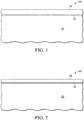
- Figure 1 sets forth a partial cross sectional side view of a wafer 100 during a stage in the manufacture of a semiconductor device according to one embodiment of the present invention.
- Wafer 100 includes a substrate 101, which in the embodiment shown, is made of a bulk monocrystalline semiconductor material such as, e.g., silicon, silicon germanium, silicon carbon, gallium nitride, gallium arsenic, another III-V semiconductor material, or another type of semiconductor material.
- substrate 101 may include conductivity dopants (N-type and P-type) implanted or formed in-situ. The conductivity dopants may be selectively implanted to form semiconductor device regions in the wafer.
- Wafer 100 may also include isolation structures (not shown) for isolating the different active regions from each other.
- substrate 101 may have a semiconductor on insulator (SOI) configuration where a buried dielectric layer (e.g. SiO 2 ) is located between an upper active semiconductor layer and a base semiconductor substrate (not shown in Figure 1 ).
- SOI semiconductor on insulator
- a thin layer 103 (e.g. 5.10 -10 meters or less equal to 5 angstroms or less) of native oxide is formed on substrate 101 from its exposure to atmosphere.
- layer 103 can be thicker and formed from an intentional oxidation or deposition process. In other embodiments, layer 103 is not present.
- a layer 105 of metal oxyhalide is formed on layer 103.
- layer 105 is formed in a deposition chamber (e.g. 402 of Figure 4 ) by the introduction of metal oxyhalide in gaseous form into the chamber at an elevated temperature.
- the material of layer 105 is deposited by an atomic layer deposition process with multiple metal oxyhalide deposition operations (also known as "pulses") with each pulse followed by a purging operation with an inert gas.
- a metal oxy halide material of layer 105 examples include hafnium oxychloride (HfOCl 2 ), hafnium oxybromide (HfOBr 2 ), hafnium oxyiodide (HfOI 2 ), hafnium oxyfluoride (HfOF 2 ), zirconium oxychloride (ZrOCl 2 ), zirconium oxybromide (ZrOBr 2 ), zirconium oxyiodide (ZrOI 2 ), zirconium oxyfluoride (ZrOF 2 ), lanthanum oxychloride (La(ClO 4 ) 3 ), lanthanum oxybromide (La(BrO 3 ) 3 ), and lanthanum oxyiodide(La(IO 3 ) 3 ), lanthanum oxyfluoride (La(FO 3 ) 3 ).
- the metal oxyhalide may include other types of metals
- layer 105 is made of a single metal oxyhalide material (e.g. hafnium oxychloride).
- layer 105 may include a number of different metal oxyhalide materials (e.g. hafnium oxychloride and zirconium oxychloride).
- the different metal oxyhalide materials may be located in contiguous separate layers of layer 105.
- each pulse of a metal oxyhalide may include a different metal oxyhalide material from the previous pulse.
- layer 105 has a thickness in the range of 10 ⁇ 10 -10 to 100 ⁇ 10 -10 meters (equal to 10 to 100 angstroms), but may have different thicknesses in other embodiments.
- each pulse of metal oxyhalide adds a thickness of material in the range of 0.1 ⁇ 10 -10 to 1 ⁇ 10 -10 meters (equal to 0.1 to 1 angstroms) to the thickness of layer 105.
- each pulse may add a different thickness of material in other embodiments.
- Figure 2 is a partial cutaway side view of wafer 100 after wafer 100 has been annealed to remove the halogens (e.g. chlorine, bromine, iodine, fluorine) of the metal oxyhalide layer 105 and other impurities from layer 105 to form a metal oxide layer 205.
- halogens e.g. chlorine, bromine, iodine, fluorine
- wafer 100 is heated to a temperature in the range of 350°C to 1100°C for a period of time in the range of 1 second to 60 seconds, but may be heated to other temperatures and/or for other times in other embodiments. It is believed that the heating of wafer 100 causes the unreacted halogens to evaporate from layer 105 and also causes the unreacted metal and oxygen to form a metal oxide.
- layer 105 densifies into layer 205 wherein the thickness of layer 205 is reduced from the thickness of layer 105 as a result of the densification process. In one embodiment, the thickness of layer 205 is reduced by a percentage in the range of 10-35% from the thickness of layer 105.
- Figure 3 is a partial cutaway side view of wafer 100 after a transistor 301 has been formed.
- a layer of gate material e.g. doped polysilicon, metal
- the layer of gate material, layer 205, and layer 103 are then patterned by a photolithographic process to form a gate stack with gate 303. The remaining portions of layers 103 and 205 form the gate dielectric for transistor 301.
- sidewall spacer 305 is formed.
- Source/drain regions 307 and 309 are then formed by implanting conductivity dopants into substrate 101. Afterwards silicide structures 313, 311 and 315 are formed by reacting a metal with the exposed silicon.
- Other processes may be performed in the forming of transistor 301 such as other etching, implanting, and cleaning processes.
- interconnect layers are formed over wafer 100.
- the interconnect layers include metal interconnects and conductive vias (not shown) to electrically couple the silicide structures (313, 315, 311) of the transistors of wafer 100 together to form circuitry and to external terminals such as bond pads that are formed over the interconnect layers.
- the interconnect layers include dielectric material that electrically isolates the interconnect structures and vias from each other. Afterwards, wafer 100 is singulated into multiple integrated circuit dies with each die including multiple transistors similar to transistor 301.
- the dies are then packaged with an encapsulant to form integrated circuit packages that can be utilized in electronic systems such as computers, cell phones, appliances, communication equipment, and automobile control systems.
- a wafer may include other devices, structures, and/or be processed by other processes. Also in other embodiments, devices of a wafer may be physically implemented in electronic systems in other configurations.
- metal oxide layer 205 is utilized as a gate dielectric for a planar MOSFET transistor 301.
- a metal oxide layer formed by the methods described herein can be used in other structures and/or for other semiconductor devices in other embodiments.
- a metal oxide layer can be used as a dielectric liner either on the substrate or in the interconnect layers, a dielectric layer separating two electrodes of a capacitor, a structure of a memory cell, or a dielectric layer in a standalone electronic component such as resistor, capacitor, or inductor.
- a metal oxide layer as formed by the methods described herein can be used with other types of transistors such as LDMOS, bipolar, finFETS, GaAs devices or GaN devices.
- a metal oxide layer can be used in the devices such as quantum well transistors and tunnel FETS.
- FIG 4 is a schematic view of a wafer processing system 401 that can be used to form a metal oxide layer similar to layer 205 on a wafer.
- System 401 includes a wafer chamber 402 where a wafer (e.g. 403) attached to a wafer chuck 405 is processed therein.
- the chamber 402 includes chamber walls 404.
- System 401 includes a controller 429 for controlling the operations of system 401.
- Located in chamber 402 is a heating element 407 for elevating the temperature of the chamber walls during wafer processing.
- Wafer chuck 405 includes a heating element 406 for elevating a temperature of the wafer during processing.
- Chamber 402 includes inlets 409 and 411 for receiving precursors in a gaseous form for forming structures on a wafer.
- inlet 409 is coupled to canister 413 and inlet 411 is coupled to canister 417.
- Each of canisters 413 and 417 is heatable by a heating element 415 and 419, respectively, to heat the precursors in the canisters to a gaseous form for flowing into chamber 402.
- each canister 413 and 417 would include a metal oxyhalide in a solid or liquid state that is heated to a gaseous state to flow into chamber 402 to be deposited on wafer 403.
- Each inlet 409 and 411 includes a purge line 421 and 425, respectively, for providing inert gases (e.g. nitrogen, argon) for purging inlets 409 and 411 and chamber 402.
- inert gases e.g. nitrogen, argon
- System 101 may also include an exhaust outlet (not shown).
- FIG 5 is a flow diagram of a process 501 for forming a metal oxide layer on a wafer according to one embodiment of the present invention. In the embodiment described below, process 501 is performed by system 401 of Figure 4 .
- Operations 502, 503 and 504 may be performed concurrently.
- metal oxyhalide material in solid or liquid form in a canister (413 or 417) is heated (with heating element 415 or 419) to a desired precursor temperature above the vapor temperature of the metal oxyhalide material to convert the metal oxyhalide into a gaseous form.
- the desired precursor temperature is in the range of 35°C to 250°C, but may be at other temperatures in other embodiments, depending on the type of precursor material.
- the metal oxyhalide material is heated under pressure in a canister in operation 502. Below is a table of melting points and/or vapor pressures of certain metal oxyhalides.
- chamber walls 404 are heated to a desired wall temperature.
- the desired wall temperature is in the range of 100°C to 200°C, but may be at other temperatures in other embodiments.
- the chamber walls 404 are heated to avoid the condensation of precursors and other materials on walls 404 during operation 505.
- wafer 403 is heated with heating element 406 to a desired wafer temperature for operation 505.
- the wafer temperature is in the range 250°C to 450°C, but may be at other temperatures in other embodiments.
- the metal oxyhalide in a gaseous form from a canister (413 or 417) is flowed into chamber 402 where it deposits on the surface of wafer 403 (the operation is referred to as a "pulse.")
- metal oxyhalide is flowed into chamber 402 for a period of time long enough to deposit a predetermined amount of metal oxyhalide material on wafer 403 (e.g. in the range of 0.1 ⁇ 10 -10 to 1 ⁇ 10 -10 meters equal to 0.1 to 1 angstroms).
- chamber 402 is purged with an inert gas in operation 507. If the metal oxyhalide that was deposited on wafer 403 in operation 505 was sourced from chamber 413, the inert gas for purging chamber 402 is provided from purge line 421. If the metal oxyhalide is sourced from chamber 417, then the inert gas is provided from purge line 425. Inert gases such as argon and nitrogen may be used for purging.
- Operations 505 and 507 are successively performed for a number of times (e.g. 100) until a desired thickness of a metal oxyhalide layer on wafer 403 is reached.
- metal oxyhalide material from both canisters 413 and 417 may be formed on wafer 403 during process 501.
- HfOCl2 may be sourced from canister 413 and ZrOCl2 may be sourced from canister 417.
- a layer containing both zirconium oxide and hafnium oxide is formed (from the anneal operation 511) on wafer 403.
- layers of the different metal oxyhalide materials can be formed during alternating pulse operations.
- a layer of one metal oxyhalide material is formed by successive pulses (operation 505) and then a second layer of a second metal oxyhalide material is subsequently formed with successive pulses.
- two metal oxyhalide materials can be flowed into chamber 402 during a single pulse operation 505 where one material comes from canister 413 and the other comes from canister 417.
- hafnium oxychloride is flowed from canister 413 and zirconium oxychloride is flowed from canister 417 concurrently during a pulse for multiple pulses to form a metal oxyhalide layer on wafer 403.
- hafnium zirconate hafnium zirconate (HfxZr1-xO2) is formed from the metal oxyhalide layer.
- the wafer is annealed by elevating the temperature of wafer 403 (e.g. with heating element 407) in operation 511.
- Annealing the wafer removes the halogens as well as other impurities from the layer and densifies the layer to a layer of metal oxides. It is believed that the annealing causes unreacted halogens to evaporate from the layer as well as causes the unreacted metal and oxygen to form a metal oxide.
- the anneal temperatures may also cause the metal oxyhalide molecules to break down, wherein the halogens are evaporated.
- the anneal operation is performed in the presence of an inert gas (e.g. argon, nitrogen).
- the anneal temperatures may range from 350°C to 1100°C, but may be at other temperatures in other embodiments.
- the anneal time maybe in the range of 1 second to 60 seconds, but may last for other time periods in other embodiments. The anneal temperature and time may depend upon the thickness and/or materials of the deposited metal oxyhalide layer.
- process shown in Figure 5 may be modified for other embodiments.
- an anneal operation (511) may follow each purge operation 507.
- some of the operations of process 501 may be performed in different chambers or with different types of equipment.
- process 501 may be performed with a different wafer processing system.
- forming a metal oxide layer from the deposition and anneal of a metal oxyhalide layer may provide for a process that has less operations than with a conventional process that uses an oxidation precursor such D 2 O, water or ozone.
- oxidation precursor pulses into the chamber and subsequent purge operations are utilized in forming the metal oxide layer.
- those extra operations may be eliminated.
- some of the operations can be performed at lower temperatures than with conventional metal oxide forming processes.
- the melting temperature of a conventional metal oxide process precursor HfCl4 is 330°C at atmospheric pressure, whereas the melting temperature of HfOCl2 is less than 200°C. Accordingly, lower temperatures may be used.
- a method comprises forming a layer of metal oxyhalide on a wafer and after the forming, annealing the wafer to remove halogens from the layer.
- the method includes forming a semiconductor device from the wafer.
- the metal oxyhalide includes hafnium and the layer include hafnium. In an example, the metal oxyhalide includes zirconium. In an example, the metal oxyhalide includes lanthanum. In an example, the layer includes hafnium zirconate after the annealing.
- the metal oxyhalide includes chlorine and the annealing includes removing chlorine from the layer.
- the metal oxyhalide s includes bromine and the annealing includes removing bromine form the layer.
- the metal oxyhalide includes iodine and the annealing includes removing iodine form the layer.
- the semiconductor device is characterized as a transistor and a portion of the layer is characterized as a gate dielectric layer of the transistor.
- the forming the layer is includes flowing a metal oxyhalide material in a gaseous form into a wafer processing chamber for deposition on the wafer in the wafer processing chamber.
- heating the metal oxyhalide material prior to the flowing the metal oxyhalide in a gaseous form, heating the metal oxyhalide material to a temperature in a range 35°C to 250°C.
- the method further comprises heating the wafer to a temperature in a range of 250°C to 450°C during the forming the layer.
- the annealing includes heating the wafer to a temperature in a range of 350°C to 1100°C in the presence of an inert gas.
- the layer is formed on a layer of semiconductor oxide material of the wafer.
- the forming the layer includes flowing a metal oxyhalide material in a gaseous form in a chamber.
- the annealing is performed while the wafer is in the chamber.
- the method further comprises after the flowing and before the annealing, purging the chamber with an inert gas.
- the wafer is in the chamber during the purging.
- the forming the layer includes flowing a metal oxyhalide material in a gaseous form in the chamber for a second time after the purging; and purging the chamber for a second time after flowing the metal oxyhalide material in gaseous form for a second time.
- the wafer is in the chamber during the purging for a second time.
- the flowing the metal oxyhalide material in the chamber includes flowing a metal oxyhalide material with a first metal.
- the flowing a metal oxyhalide material in the chamber for a second time includes a flowing a metal oxyhalide material with a second metal different than the first metal.
- the first metal is one of zirconium and hafnium and the second metal is the other of zirconium and hafnium.
- a method in another embodiment, includes forming a layer of metal oxyhalide on a wafer in a chamber.
- the forming a layer comprising performing a sequence of operations a plurality of times.
- the sequence of operations includes flowing a metal oxyhalide material in a gaseous form into the chamber with the wafer to deposit metal oxyhalide on the wafer and after the flowing, purging the chamber with an inert gas.
- the method includes after the forming the layer, annealing the wafer to remove halogens from the layer. After the annealing, the layer includes a metal oxide.
- the method includes forming a semiconductor device with the layer including the metal oxide.
- the semiconductor device may be characterized as a transistor and a portion of the layer is characterized as a gate dielectric layer of the transistor.
Landscapes
- Chemical & Material Sciences (AREA)
- General Chemical & Material Sciences (AREA)
- Chemical Kinetics & Catalysis (AREA)
- Engineering & Computer Science (AREA)
- Materials Engineering (AREA)
- Mechanical Engineering (AREA)
- Metallurgy (AREA)
- Organic Chemistry (AREA)
- Inorganic Chemistry (AREA)
- Formation Of Insulating Films (AREA)
- Insulated Gate Type Field-Effect Transistor (AREA)
Abstract
Description
- This invention relates to a method for making a metal oxide layer on a wafer.
- Metal oxides are utilized for semiconductor devices such as transistors. In some examples, metal oxides can be used as gate dielectric layers that have a higher dielectric constant than silicon dioxide.
- The present invention may be better understood, and its numerous objects, features, and advantages made apparent to those skilled in the art by referencing the accompanying drawings.
-
Figures 1-3 set forth cutaway side views of various stages in the formation of a semiconductor device according to one embodiment of the present invention. -
Figure 4 is a schematic view of a wafer processing system. -
Figure 5 is a flow diagram of a process for forming a metal oxide according to one embodiment of the present invention. - The use of the same reference symbols in different drawings indicates identical items unless otherwise noted. The Figures are not necessarily drawn to scale.
- The following sets forth a detailed description of a mode for carrying out the invention. The description is intended to be illustrative of the invention and should not be taken to be limiting.
- Described herein are methods for forming a metal oxide layer on a wafer. In some embodiments, the methods include forming a layer of metal oxyhalide on a wafer followed by an anneal of the wafer which removes halogens from the layer to form a densified layer of metal oxide. In some embodiments, the layer of metal oxyhalide is formed on a wafer in a chamber by a number of metal oxyhalide deposition operations, each of which is followed by an inert gas purge operation in the chamber. Afterwards, the wafer is annealed to remove halogens from the layer of metal oxyhalide.
- In some embodiments, the processes described herein allow for the formation of a metal oxide layer on a wafer without the use of a separate oxidizing agent such as water or ozone. Some conventional metal oxide formation processes utilize an oxidizing agent (e.g. water, deuterium oxide (D2O), ozone) and a metal halide precursor (e.g. HfCl4, ZrCl4). Providing a process for forming a metal oxide layer without the use of an oxidizing agent may in some embodiments, reduce the number of operations needed to form a metal oxide layer.
-
Figure 1 sets forth a partial cross sectional side view of awafer 100 during a stage in the manufacture of a semiconductor device according to one embodiment of the present invention. Wafer 100 includes asubstrate 101, which in the embodiment shown, is made of a bulk monocrystalline semiconductor material such as, e.g., silicon, silicon germanium, silicon carbon, gallium nitride, gallium arsenic, another III-V semiconductor material, or another type of semiconductor material. In some embodiments,substrate 101 may include conductivity dopants (N-type and P-type) implanted or formed in-situ. The conductivity dopants may be selectively implanted to form semiconductor device regions in the wafer.Wafer 100 may also include isolation structures (not shown) for isolating the different active regions from each other. In other embodiments,substrate 101 may have a semiconductor on insulator (SOI) configuration where a buried dielectric layer (e.g. SiO2) is located between an upper active semiconductor layer and a base semiconductor substrate (not shown inFigure 1 ). - A thin layer 103 (e.g. 5.10-10 meters or less equal to 5 angstroms or less) of native oxide is formed on
substrate 101 from its exposure to atmosphere. In some embodiments,layer 103 can be thicker and formed from an intentional oxidation or deposition process. In other embodiments,layer 103 is not present. - A layer 105 of metal oxyhalide is formed on
layer 103. In one embodiment, layer 105 is formed in a deposition chamber (e.g. 402 ofFigure 4 ) by the introduction of metal oxyhalide in gaseous form into the chamber at an elevated temperature. In some embodiments, the material of layer 105 is deposited by an atomic layer deposition process with multiple metal oxyhalide deposition operations (also known as "pulses") with each pulse followed by a purging operation with an inert gas. - Some examples of a metal oxy halide material of layer 105 include hafnium oxychloride (HfOCl2), hafnium oxybromide (HfOBr2), hafnium oxyiodide (HfOI2), hafnium oxyfluoride (HfOF2), zirconium oxychloride (ZrOCl2), zirconium oxybromide (ZrOBr2), zirconium oxyiodide (ZrOI2), zirconium oxyfluoride (ZrOF2), lanthanum oxychloride (La(ClO4)3), lanthanum oxybromide (La(BrO3)3), and lanthanum oxyiodide(La(IO3)3), lanthanum oxyfluoride (La(FO3)3). In other embodiments, the metal oxyhalide may include other types of metals such as Al, Sc, Ti, V, Y, Ta, W, Ce, Gd, etc. and/or include other types of halogens.
- In one embodiment, layer 105 is made of a single metal oxyhalide material (e.g. hafnium oxychloride). In other embodiments, layer 105 may include a number of different metal oxyhalide materials (e.g. hafnium oxychloride and zirconium oxychloride). In one embodiment, the different metal oxyhalide materials may be located in contiguous separate layers of layer 105. In other embodiments, each pulse of a metal oxyhalide may include a different metal oxyhalide material from the previous pulse.
- In one embodiment, layer 105 has a thickness in the range of 10·10-10 to 100·10-10 meters (equal to 10 to 100 angstroms), but may have different thicknesses in other embodiments. In some embodiments, each pulse of metal oxyhalide adds a thickness of material in the range of 0.1·10-10 to 1·10-10 meters (equal to 0.1 to 1 angstroms) to the thickness of layer 105. However, each pulse may add a different thickness of material in other embodiments.
-
Figure 2 is a partial cutaway side view ofwafer 100 afterwafer 100 has been annealed to remove the halogens (e.g. chlorine, bromine, iodine, fluorine) of the metal oxyhalide layer 105 and other impurities from layer 105 to form ametal oxide layer 205. In one embodiment, during the anneal process,wafer 100 is heated to a temperature in the range of 350°C to 1100°C for a period of time in the range of 1 second to 60 seconds, but may be heated to other temperatures and/or for other times in other embodiments. It is believed that the heating ofwafer 100 causes the unreacted halogens to evaporate from layer 105 and also causes the unreacted metal and oxygen to form a metal oxide. Some possible reactions with the metal oxyhalide layer during the annealing process are as follows:
HfOCl2 ---→ HfO2 (S) + Cl2 (g);
HfOBr2 ---→ HfO2 (S) + Br2 (g);
ZrOCl2 ---→ ZrO2 (S) + Cl2 (g);
ZrOBr2 ---→ ZrO2 (S) + Br2 (g);
where S= solid, g = gas. - During the annealing process, layer 105 densifies into
layer 205 wherein the thickness oflayer 205 is reduced from the thickness of layer 105 as a result of the densification process. In one embodiment, the thickness oflayer 205 is reduced by a percentage in the range of 10-35% from the thickness of layer 105. -
Figure 3 is a partial cutaway side view ofwafer 100 after atransistor 301 has been formed. After the annealing process, a layer of gate material (e.g. doped polysilicon, metal) is formed onlayer 205. The layer of gate material,layer 205, andlayer 103 are then patterned by a photolithographic process to form a gate stack withgate 303. The remaining portions oflayers transistor 301. After the patterning of the gate material layer,sidewall spacer 305 is formed. Source/drain regions substrate 101. Afterwardssilicide structures transistor 301 such as other etching, implanting, and cleaning processes. - After the stage shown in
Figure 3 , interconnect layers (not shown) are formed overwafer 100. The interconnect layers include metal interconnects and conductive vias (not shown) to electrically couple the silicide structures (313, 315, 311) of the transistors ofwafer 100 together to form circuitry and to external terminals such as bond pads that are formed over the interconnect layers. The interconnect layers include dielectric material that electrically isolates the interconnect structures and vias from each other. Afterwards,wafer 100 is singulated into multiple integrated circuit dies with each die including multiple transistors similar totransistor 301. - The dies are then packaged with an encapsulant to form integrated circuit packages that can be utilized in electronic systems such as computers, cell phones, appliances, communication equipment, and automobile control systems.
- In other embodiments, a wafer may include other devices, structures, and/or be processed by other processes. Also in other embodiments, devices of a wafer may be physically implemented in electronic systems in other configurations.
- In the embodiment of
Figure 3 ,metal oxide layer 205 is utilized as a gate dielectric for aplanar MOSFET transistor 301. However, in other embodiments, a metal oxide layer formed by the methods described herein can be used in other structures and/or for other semiconductor devices in other embodiments. For example, a metal oxide layer can be used as a dielectric liner either on the substrate or in the interconnect layers, a dielectric layer separating two electrodes of a capacitor, a structure of a memory cell, or a dielectric layer in a standalone electronic component such as resistor, capacitor, or inductor. For example, a metal oxide layer as formed by the methods described herein can be used with other types of transistors such as LDMOS, bipolar, finFETS, GaAs devices or GaN devices. Also, a metal oxide layer can be used in the devices such as quantum well transistors and tunnel FETS. -
Figure 4 is a schematic view of awafer processing system 401 that can be used to form a metal oxide layer similar tolayer 205 on a wafer.System 401 includes awafer chamber 402 where a wafer (e.g. 403) attached to awafer chuck 405 is processed therein. Thechamber 402 includeschamber walls 404.System 401 includes acontroller 429 for controlling the operations ofsystem 401. Located inchamber 402 is aheating element 407 for elevating the temperature of the chamber walls during wafer processing.Wafer chuck 405 includes aheating element 406 for elevating a temperature of the wafer during processing. -
Chamber 402 includesinlets inlet 409 is coupled tocanister 413 andinlet 411 is coupled tocanister 417. Each ofcanisters heating element chamber 402. In one embodiment, eachcanister chamber 402 to be deposited onwafer 403. Eachinlet purge line inlets chamber 402. In other embodiments, other types of wafer processing systems can be used to form a metal oxide layer.System 101 may also include an exhaust outlet (not shown). -
Figure 5 is a flow diagram of aprocess 501 for forming a metal oxide layer on a wafer according to one embodiment of the present invention. In the embodiment described below,process 501 is performed bysystem 401 ofFigure 4 . -
Operations operation 502, metal oxyhalide material in solid or liquid form in a canister (413 or 417) is heated (withheating element 415 or 419) to a desired precursor temperature above the vapor temperature of the metal oxyhalide material to convert the metal oxyhalide into a gaseous form. In one embodiment, the desired precursor temperature is in the range of 35°C to 250°C, but may be at other temperatures in other embodiments, depending on the type of precursor material. In some embodiments, the metal oxyhalide material is heated under pressure in a canister inoperation 502. Below is a table of melting points and/or vapor pressures of certain metal oxyhalides.Metal Oxyhalide Melting point or, Vapor pressure HfOCl2 < 200 C ZrOCl2 150 C HfOBr2 120 C La(ClO4)3 55 C @ 86 Torr La(BrO3)3 37.5 C La(IO3)3 > 800 C - In
operation 503,chamber walls 404 are heated to a desired wall temperature. In one embodiment, the desired wall temperature is in the range of 100°C to 200°C, but may be at other temperatures in other embodiments. Thechamber walls 404 are heated to avoid the condensation of precursors and other materials onwalls 404 duringoperation 505. - In
operation 504,wafer 403 is heated withheating element 406 to a desired wafer temperature foroperation 505. In one embodiment, the wafer temperature is in the range 250°C to 450°C, but may be at other temperatures in other embodiments. - In
operation 505, the metal oxyhalide in a gaseous form from a canister (413 or 417) is flowed intochamber 402 where it deposits on the surface of wafer 403 (the operation is referred to as a "pulse.") In one embodiment, metal oxyhalide is flowed intochamber 402 for a period of time long enough to deposit a predetermined amount of metal oxyhalide material on wafer 403 (e.g. in the range of 0.1·10-10 to 1·10-10 meters equal to 0.1 to 1 angstroms). - After
operation 505,chamber 402 is purged with an inert gas inoperation 507. If the metal oxyhalide that was deposited onwafer 403 inoperation 505 was sourced fromchamber 413, the inert gas for purgingchamber 402 is provided frompurge line 421. If the metal oxyhalide is sourced fromchamber 417, then the inert gas is provided frompurge line 425. Inert gases such as argon and nitrogen may be used for purging. -
Operations wafer 403 is reached. In some embodiments, metal oxyhalide material from bothcanisters wafer 403 duringprocess 501. For example, in some embodiments, HfOCl2 may be sourced fromcanister 413 and ZrOCl2 may be sourced fromcanister 417. In such embodiments, a layer containing both zirconium oxide and hafnium oxide is formed (from the anneal operation 511) onwafer 403. In some embodiments, layers of the different metal oxyhalide materials can be formed during alternating pulse operations. In other embodiments, a layer of one metal oxyhalide material is formed by successive pulses (operation 505) and then a second layer of a second metal oxyhalide material is subsequently formed with successive pulses. In still other embodiments, two metal oxyhalide materials can be flowed intochamber 402 during asingle pulse operation 505 where one material comes fromcanister 413 and the other comes fromcanister 417. In one embodiment, hafnium oxychloride is flowed fromcanister 413 and zirconium oxychloride is flowed fromcanister 417 concurrently during a pulse for multiple pulses to form a metal oxyhalide layer onwafer 403. In a subsequent anneal step, hafnium zirconate (HfxZr1-xO2) is formed from the metal oxyhalide layer. - In the embodiment shown, after a layer of metal oxyhalide is formed on
wafer 403, the wafer is annealed by elevating the temperature of wafer 403 (e.g. with heating element 407) in operation 511. Annealing the wafer removes the halogens as well as other impurities from the layer and densifies the layer to a layer of metal oxides. It is believed that the annealing causes unreacted halogens to evaporate from the layer as well as causes the unreacted metal and oxygen to form a metal oxide. The anneal temperatures may also cause the metal oxyhalide molecules to break down, wherein the halogens are evaporated. The anneal operation is performed in the presence of an inert gas (e.g. argon, nitrogen). In some embodiments, the anneal temperatures may range from 350°C to 1100°C, but may be at other temperatures in other embodiments. In some embodiments, the anneal time maybe in the range of 1 second to 60 seconds, but may last for other time periods in other embodiments. The anneal temperature and time may depend upon the thickness and/or materials of the deposited metal oxyhalide layer. After the anneal operation 511, the chamber is purged with an inert gas inoperation 513. - The process shown in
Figure 5 may be modified for other embodiments. For example, in some embodiments, an anneal operation (511) may follow eachpurge operation 507. Furthermore, in some embodiments, some of the operations ofprocess 501 may be performed in different chambers or with different types of equipment. In other embodiments,process 501 may be performed with a different wafer processing system. - As stated above, forming a metal oxide layer from the deposition and anneal of a metal oxyhalide layer in some embodiments, may provide for a process that has less operations than with a conventional process that uses an oxidation precursor such D2O, water or ozone. With some conventional processes, oxidation precursor pulses into the chamber and subsequent purge operations are utilized in forming the metal oxide layer. With at least some of the processes described herein, those extra operations may be eliminated.
- Also, in some embodiments of the processes described herein, some of the operations can be performed at lower temperatures than with conventional metal oxide forming processes. For example, the melting temperature of a conventional metal oxide process precursor HfCl4 is 330°C at atmospheric pressure, whereas the melting temperature of HfOCl2 is less than 200°C. Accordingly, lower temperatures may be used.
- In one embodiment, a method comprises forming a layer of metal oxyhalide on a wafer and after the forming, annealing the wafer to remove halogens from the layer. The method includes forming a semiconductor device from the wafer.
- In an example, the metal oxyhalide includes hafnium and the layer include hafnium. In an example, the metal oxyhalide includes zirconium. In an example, the metal oxyhalide includes lanthanum. In an example, the layer includes hafnium zirconate after the annealing.
- In an example, the metal oxyhalide includes chlorine and the annealing includes removing chlorine from the layer. In an example, the metal oxyhalide s includes bromine and the annealing includes removing bromine form the layer. In an example, the metal oxyhalide includes iodine and the annealing includes removing iodine form the layer.
- In an example, the semiconductor device is characterized as a transistor and a portion of the layer is characterized as a gate dielectric layer of the transistor.
- In an example, the forming the layer is includes flowing a metal oxyhalide material in a gaseous form into a wafer processing chamber for deposition on the wafer in the wafer processing chamber.
- In an example, prior to the flowing the metal oxyhalide in a gaseous form, heating the metal oxyhalide material to a temperature in a range 35°C to 250°C. In an example, the method further comprises heating the wafer to a temperature in a range of 250°C to 450°C during the forming the layer. In an example, the annealing includes heating the wafer to a temperature in a range of 350°C to 1100°C in the presence of an inert gas.
- In an example, the layer is formed on a layer of semiconductor oxide material of the wafer.
- In an example, the forming the layer includes flowing a metal oxyhalide material in a gaseous form in a chamber. The annealing is performed while the wafer is in the chamber. The method further comprises after the flowing and before the annealing, purging the chamber with an inert gas. The wafer is in the chamber during the purging. In an example, the forming the layer includes flowing a metal oxyhalide material in a gaseous form in the chamber for a second time after the purging; and purging the chamber for a second time after flowing the metal oxyhalide material in gaseous form for a second time. The wafer is in the chamber during the purging for a second time. In an example, the flowing the metal oxyhalide material in the chamber includes flowing a metal oxyhalide material with a first metal. The flowing a metal oxyhalide material in the chamber for a second time includes a flowing a metal oxyhalide material with a second metal different than the first metal. In an example, the first metal is one of zirconium and hafnium and the second metal is the other of zirconium and hafnium.
- In another embodiment, a method includes forming a layer of metal oxyhalide on a wafer in a chamber. The forming a layer comprising performing a sequence of operations a plurality of times. The sequence of operations includes flowing a metal oxyhalide material in a gaseous form into the chamber with the wafer to deposit metal oxyhalide on the wafer and after the flowing, purging the chamber with an inert gas. The method includes after the forming the layer, annealing the wafer to remove halogens from the layer. After the annealing, the layer includes a metal oxide. The method includes forming a semiconductor device with the layer including the metal oxide. The semiconductor device may be characterized as a transistor and a portion of the layer is characterized as a gate dielectric layer of the transistor.
- Features shown or described with respect to one embodiment may be implemented with other embodiments shown or described herein. Features claimed in separate claims may be combined in any appropriate combinations to form other embodiments. While particular embodiments of the present invention have been shown and described, it will be recognized to those skilled in the art that, based upon the teachings herein, further changes and modifications may be made without departing from this invention and its broader aspects, and thus, the appended claims are to encompass within their scope all such changes and modifications as are within the true spirit and scope of this invention.
Claims (15)
- A method comprising:forming a layer (105) of metal oxyhalide on a wafer (100);after the forming, annealing the wafer (100) to remove halogens from the layer (105, 205);forming a semiconductor device from the wafer (105).
- The method of claim 1, wherein:the metal oxyhalide includes hafnium and the layer (105) include hafnium;the metal oxyhalide includes zirconium; orthe metal oxyhalide includes and lanthanum.
- The method of claim 1 or claim 2, wherein:the metal oxyhalide includes chlorine and the annealing includes removing chlorine from the layer (105, 205);wherein the metal oxyhalide s includes bromine and the annealing includes removing bromine form the layer (105, 205); and/orwherein the metal oxyhalide includes iodine and the annealing includes removing iodine form the layer (105, 205).
- The method of any preceding claim, wherein the semiconductor device is characterized as a transistor (301) and a portion of the layer (205) is characterized as a gate dielectric layer of the transistor (301).
- The method of any preceding claim, wherein the layer (105, 205) includes hafnium zirconate after the annealing.
- The method of any preceding claim, wherein the forming the layer (105) is includes flowing a metal oxyhalide material in a gaseous form into a wafer processing chamber (402) for deposition on the wafer (100) in the wafer processing chamber (402).
- The method of claim 6, wherein prior to the flowing the metal oxyhalide in a gaseous form, heating the metal oxyhalide material to a temperature in a range 35°C to 250°C.
- The method of claim 6 or claim 7, further comprising heating the wafer (100) to a temperature in a range of 250°C to 450°C during the forming the layer (105).
- The method of any preceding claim, wherein the layer (105) is formed on a layer (103) of semiconductor oxide material of the wafer (100).
- The method of any preceding claim, wherein the annealing includes heating the wafer (100) to a temperature in a range of 350°C to 1100°C in the presence of an inert gas.
- The method of any one of the claims 6 to 10, wherein the annealing is performed while the wafer (100) is in the chamber (402), the method further comprising after the flowing and before the annealing, purging the chamber (402) with an inert gas, wherein the wafer (100) is in the chamber (402) during the purging.
- The method of claim 11, wherein the forming the layer (105) includes:flowing a metal oxyhalide material in a gaseous form in the chamber (402) for a second time after the purging;purging the chamber (402) for a second time after flowing the metal oxyhalide material in gaseous form for a second time, wherein the wafer (100) is in the chamber (402) during the purging for a second time.
- The method of claim 12, wherein the flowing the metal oxyhalide material in the chamber (402) includes flowing a metal oxyhalide material with a first metal, wherein the flowing a metal oxyhalide material in the chamber (402) for a second time includes a flowing a metal oxyhalide material with a second metal different than the first metal.
- The method of claim 13, wherein the first metal is one of zirconium and hafnium and the second metal is the other of zirconium and hafnium.
- A method comprising:forming a layer (105) of metal oxyhalide on a wafer (100) in a chamber (402), the forming a layer (105) comprising performing a sequence of operations a plurality of times, the sequence of operations comprising:flowing a metal oxyhalide material in a gaseous form into the chamber (402) with the wafer (100) to deposit metal oxyhalide on the wafer (100);after the flowing, purging the chamber (402) with an inert gas;after the forming the layer (105), annealing the wafer (100) to remove halogens from the layer (105, 205), wherein after the annealing, the layer (205) includes a metal oxide;forming a semiconductor device with the layer (205) including the metal oxide.
Applications Claiming Priority (1)
| Application Number | Priority Date | Filing Date | Title |
|---|---|---|---|
| US15/615,884 US10121652B1 (en) | 2017-06-07 | 2017-06-07 | Formation of metal oxide layer |
Publications (2)
| Publication Number | Publication Date |
|---|---|
| EP3413333A1 true EP3413333A1 (en) | 2018-12-12 |
| EP3413333B1 EP3413333B1 (en) | 2020-06-10 |
Family
ID=61952572
Family Applications (1)
| Application Number | Title | Priority Date | Filing Date |
|---|---|---|---|
| EP18166149.7A Active EP3413333B1 (en) | 2017-06-07 | 2018-04-06 | Formation of metal oxide layer |
Country Status (3)
| Country | Link |
|---|---|
| US (1) | US10121652B1 (en) |
| EP (1) | EP3413333B1 (en) |
| CN (1) | CN109003881B (en) |
Families Citing this family (1)
| Publication number | Priority date | Publication date | Assignee | Title |
|---|---|---|---|---|
| CN112928210B (en) | 2021-02-03 | 2022-04-15 | 长鑫存储技术有限公司 | Capacitor structure and preparation method thereof |
Citations (2)
| Publication number | Priority date | Publication date | Assignee | Title |
|---|---|---|---|---|
| US20130313656A1 (en) * | 2012-05-24 | 2013-11-28 | Intermolecular, Inc. | Methods of atomic layer deposition of hafnium oxide / erbium oxide bi-layer as advanced gate dielectrics |
| US20130313657A1 (en) * | 2012-05-24 | 2013-11-28 | Intermolecular, Inc. | Methods of forming fluorinated hafnium oxide gate dielectrics by atomic layer deposition |
Family Cites Families (16)
| Publication number | Priority date | Publication date | Assignee | Title |
|---|---|---|---|---|
| US3546128A (en) * | 1968-10-23 | 1970-12-08 | Gen Electric | Lanthanum and gadolinium oxybromide luminescent materials activated with erbium |
| US4931312A (en) * | 1986-02-10 | 1990-06-05 | North American Philips Corporation | Sol-gel process for producing liminescent thin film, and film so produced and devices utilizing same |
| JPH0326276A (en) * | 1989-06-23 | 1991-02-04 | Junkosha Co Ltd | Contrast medium-containing tube |
| US5024859A (en) | 1989-11-20 | 1991-06-18 | General Electric Company | Method for applying an oxide barrier coating to a reinforcing fiber |
| US5786031A (en) * | 1995-06-07 | 1998-07-28 | Engelhard Corporation | Barrier for a metal substrate |
| US6250540B1 (en) * | 1999-04-30 | 2001-06-26 | International Business Machines Corporation | Fluxless joining process for enriched solders |
| JP2001261465A (en) * | 2000-03-16 | 2001-09-26 | Ngk Insulators Ltd | Production process of ceramic porous filter |
| JP2001261464A (en) * | 2000-03-16 | 2001-09-26 | Ngk Insulators Ltd | Production process of ceramic porous filter |
| US20040011380A1 (en) * | 2002-07-18 | 2004-01-22 | Bing Ji | Method for etching high dielectric constant materials and for cleaning deposition chambers for high dielectric constant materials |
| US20040168627A1 (en) * | 2003-02-27 | 2004-09-02 | Sharp Laboratories Of America, Inc. | Atomic layer deposition of oxide film |
| WO2006137898A2 (en) * | 2004-10-01 | 2006-12-28 | American Superconductor Corp. | Thick superconductor films with improved performance |
| JP4911455B2 (en) * | 2006-09-27 | 2012-04-04 | 富士フイルム株式会社 | Photopolymerization type photosensitive lithographic printing plate precursor |
| WO2013068243A1 (en) * | 2011-11-07 | 2013-05-16 | Solvay Sa | A catalyst for direct synthesis of hydrogen peroxide comprising zirconium oxide |
| US9663400B2 (en) * | 2013-11-08 | 2017-05-30 | Corning Incorporated | Scratch-resistant liquid based coatings for glass |
| US9252233B2 (en) * | 2014-03-12 | 2016-02-02 | Taiwan Semiconductor Manufacturing Co., Ltd. | Air-gap offset spacer in FinFET structure |
| CN106653844A (en) * | 2015-11-03 | 2017-05-10 | 中芯国际集成电路制造(上海)有限公司 | Fin field effect transistor and forming method thereof |
-
2017
- 2017-06-07 US US15/615,884 patent/US10121652B1/en active Active
-
2018
- 2018-04-06 EP EP18166149.7A patent/EP3413333B1/en active Active
- 2018-06-06 CN CN201810579777.6A patent/CN109003881B/en active Active
Patent Citations (2)
| Publication number | Priority date | Publication date | Assignee | Title |
|---|---|---|---|---|
| US20130313656A1 (en) * | 2012-05-24 | 2013-11-28 | Intermolecular, Inc. | Methods of atomic layer deposition of hafnium oxide / erbium oxide bi-layer as advanced gate dielectrics |
| US20130313657A1 (en) * | 2012-05-24 | 2013-11-28 | Intermolecular, Inc. | Methods of forming fluorinated hafnium oxide gate dielectrics by atomic layer deposition |
Non-Patent Citations (3)
| Title |
|---|
| KAUPO KUKLI: "Atomic layer deposition of HfO2 thin films and nanolayered HfO2-Al2O3-Nb2O5 dielectrics", JOURNAL OF MATERIALS SCIENCE. MATERIALS IN ELECTRONICS., vol. 14, no. 5/7, 1 January 2003 (2003-01-01), GB, pages 361 - 367, XP055243445, ISSN: 0957-4522, DOI: 10.1023/A:1023948617372 * |
| KUKLI KAUPO ET AL: "Influence of growth temperature on properties of zirconium dioxide films grown by atomic layer deposition", JOURNAL OF APPLIED PHYSICS, AMERICAN INSTITUTE OF PHYSICS, US, vol. 92, no. 4, 15 August 2002 (2002-08-15), pages 1833 - 1840, XP012057038, ISSN: 0021-8979, DOI: 10.1063/1.1493657 * |
| SUN QING-QING ET AL: "Effects of chlorine residue in atomic layer deposition hafnium oxide: A density-functional-theory study", APPLIED PHYSICS LETTERS, A I P PUBLISHING LLC, US, vol. 91, no. 2, 9 July 2007 (2007-07-09), pages 22901 - 22901, XP012100062, ISSN: 0003-6951, DOI: 10.1063/1.2756108 * |
Also Published As
| Publication number | Publication date |
|---|---|
| US10121652B1 (en) | 2018-11-06 |
| CN109003881A (en) | 2018-12-14 |
| CN109003881B (en) | 2023-10-24 |
| EP3413333B1 (en) | 2020-06-10 |
Similar Documents
| Publication | Publication Date | Title |
|---|---|---|
| US11848369B2 (en) | Horizontal gate-all-around device nanowire air gap spacer formation | |
| US10269571B2 (en) | Methods for fabricating nanowire for semiconductor applications | |
| US9441298B2 (en) | Devices including metal-silicon contacts using indium arsenide films and apparatus and methods | |
| US6911707B2 (en) | Ultrathin high-K gate dielectric with favorable interface properties for improved semiconductor device performance | |
| US7385265B2 (en) | High dielectric constant MOSFET device | |
| US9484406B1 (en) | Method for fabricating nanowires for horizontal gate all around devices for semiconductor applications | |
| US7622401B2 (en) | Method of producing insulator thin film, insulator thin film, method of manufacturing semiconductor device, and semiconductor device | |
| CN101471254B (en) | Method for forming dielectric films | |
| KR102809766B1 (en) | MOSFET Gate Engineering Using Dipolar Films | |
| CN100411116C (en) | Method for forming dielectric film | |
| US20150132938A1 (en) | Methods and Systems for Forming Reliable Gate Stack on Semiconductors | |
| JP2001237243A (en) | Method and process for manufacturing in-situ dielectric stack | |
| WO2014035933A1 (en) | Methods and apparatus for forming tantalum silicate layers on germanium or iii-v semiconductor devices | |
| US11018223B2 (en) | Methods for forming device isolation for semiconductor applications | |
| CN106504991B (en) | Method for fabricating nanowires for horizontal full-ring gate devices for semiconductor applications | |
| KR100944831B1 (en) | Manufacturing Method and Film Forming Device of Semiconductor Device | |
| US8633119B2 (en) | Methods for manufacturing high dielectric constant films | |
| US8633114B2 (en) | Methods for manufacturing high dielectric constant films | |
| US10121652B1 (en) | Formation of metal oxide layer | |
| US6218315B1 (en) | HTO (high temperature oxide) deposition for capacitor dielectrics | |
| CN1689146B (en) | Semiconductor device and manufacturing method thereof | |
| TW202412185A (en) | Barrier layer for preventing aluminum diffusion | |
| KR102857454B1 (en) | Amorphous silicon-based scavenging and sealing EOT | |
| JP4416354B2 (en) | Semiconductor device manufacturing method and manufacturing apparatus thereof | |
| US20040135218A1 (en) | MOS transistor with high k gate dielectric |
Legal Events
| Date | Code | Title | Description |
|---|---|---|---|
| PUAI | Public reference made under article 153(3) epc to a published international application that has entered the european phase |
Free format text: ORIGINAL CODE: 0009012 |
|
| STAA | Information on the status of an ep patent application or granted ep patent |
Free format text: STATUS: THE APPLICATION HAS BEEN PUBLISHED |
|
| AK | Designated contracting states |
Kind code of ref document: A1 Designated state(s): AL AT BE BG CH CY CZ DE DK EE ES FI FR GB GR HR HU IE IS IT LI LT LU LV MC MK MT NL NO PL PT RO RS SE SI SK SM TR |
|
| AX | Request for extension of the european patent |
Extension state: BA ME |
|
| STAA | Information on the status of an ep patent application or granted ep patent |
Free format text: STATUS: REQUEST FOR EXAMINATION WAS MADE |
|
| 17P | Request for examination filed |
Effective date: 20190612 |
|
| RBV | Designated contracting states (corrected) |
Designated state(s): AL AT BE BG CH CY CZ DE DK EE ES FI FR GB GR HR HU IE IS IT LI LT LU LV MC MK MT NL NO PL PT RO RS SE SI SK SM TR |
|
| STAA | Information on the status of an ep patent application or granted ep patent |
Free format text: STATUS: EXAMINATION IS IN PROGRESS |
|
| 17Q | First examination report despatched |
Effective date: 20190923 |
|
| GRAP | Despatch of communication of intention to grant a patent |
Free format text: ORIGINAL CODE: EPIDOSNIGR1 |
|
| STAA | Information on the status of an ep patent application or granted ep patent |
Free format text: STATUS: GRANT OF PATENT IS INTENDED |
|
| INTG | Intention to grant announced |
Effective date: 20200302 |
|
| GRAS | Grant fee paid |
Free format text: ORIGINAL CODE: EPIDOSNIGR3 |
|
| GRAA | (expected) grant |
Free format text: ORIGINAL CODE: 0009210 |
|
| STAA | Information on the status of an ep patent application or granted ep patent |
Free format text: STATUS: THE PATENT HAS BEEN GRANTED |
|
| AK | Designated contracting states |
Kind code of ref document: B1 Designated state(s): AL AT BE BG CH CY CZ DE DK EE ES FI FR GB GR HR HU IE IS IT LI LT LU LV MC MK MT NL NO PL PT RO RS SE SI SK SM TR |
|
| REG | Reference to a national code |
Ref country code: GB Ref legal event code: FG4D |
|
| REG | Reference to a national code |
Ref country code: CH Ref legal event code: EP Ref country code: AT Ref legal event code: REF Ref document number: 1279858 Country of ref document: AT Kind code of ref document: T Effective date: 20200615 |
|
| REG | Reference to a national code |
Ref country code: DE Ref legal event code: R096 Ref document number: 602018005136 Country of ref document: DE |
|
| REG | Reference to a national code |
Ref country code: IE Ref legal event code: FG4D |
|
| REG | Reference to a national code |
Ref country code: LT Ref legal event code: MG4D |
|
| PG25 | Lapsed in a contracting state [announced via postgrant information from national office to epo] |
Ref country code: GR Free format text: LAPSE BECAUSE OF FAILURE TO SUBMIT A TRANSLATION OF THE DESCRIPTION OR TO PAY THE FEE WITHIN THE PRESCRIBED TIME-LIMIT Effective date: 20200911 Ref country code: LT Free format text: LAPSE BECAUSE OF FAILURE TO SUBMIT A TRANSLATION OF THE DESCRIPTION OR TO PAY THE FEE WITHIN THE PRESCRIBED TIME-LIMIT Effective date: 20200610 Ref country code: SE Free format text: LAPSE BECAUSE OF FAILURE TO SUBMIT A TRANSLATION OF THE DESCRIPTION OR TO PAY THE FEE WITHIN THE PRESCRIBED TIME-LIMIT Effective date: 20200610 Ref country code: NO Free format text: LAPSE BECAUSE OF FAILURE TO SUBMIT A TRANSLATION OF THE DESCRIPTION OR TO PAY THE FEE WITHIN THE PRESCRIBED TIME-LIMIT Effective date: 20200910 Ref country code: FI Free format text: LAPSE BECAUSE OF FAILURE TO SUBMIT A TRANSLATION OF THE DESCRIPTION OR TO PAY THE FEE WITHIN THE PRESCRIBED TIME-LIMIT Effective date: 20200610 |
|
| REG | Reference to a national code |
Ref country code: NL Ref legal event code: MP Effective date: 20200610 |
|
| PG25 | Lapsed in a contracting state [announced via postgrant information from national office to epo] |
Ref country code: HR Free format text: LAPSE BECAUSE OF FAILURE TO SUBMIT A TRANSLATION OF THE DESCRIPTION OR TO PAY THE FEE WITHIN THE PRESCRIBED TIME-LIMIT Effective date: 20200610 Ref country code: LV Free format text: LAPSE BECAUSE OF FAILURE TO SUBMIT A TRANSLATION OF THE DESCRIPTION OR TO PAY THE FEE WITHIN THE PRESCRIBED TIME-LIMIT Effective date: 20200610 Ref country code: RS Free format text: LAPSE BECAUSE OF FAILURE TO SUBMIT A TRANSLATION OF THE DESCRIPTION OR TO PAY THE FEE WITHIN THE PRESCRIBED TIME-LIMIT Effective date: 20200610 Ref country code: BG Free format text: LAPSE BECAUSE OF FAILURE TO SUBMIT A TRANSLATION OF THE DESCRIPTION OR TO PAY THE FEE WITHIN THE PRESCRIBED TIME-LIMIT Effective date: 20200910 |
|
| REG | Reference to a national code |
Ref country code: AT Ref legal event code: MK05 Ref document number: 1279858 Country of ref document: AT Kind code of ref document: T Effective date: 20200610 |
|
| PG25 | Lapsed in a contracting state [announced via postgrant information from national office to epo] |
Ref country code: AL Free format text: LAPSE BECAUSE OF FAILURE TO SUBMIT A TRANSLATION OF THE DESCRIPTION OR TO PAY THE FEE WITHIN THE PRESCRIBED TIME-LIMIT Effective date: 20200610 Ref country code: NL Free format text: LAPSE BECAUSE OF FAILURE TO SUBMIT A TRANSLATION OF THE DESCRIPTION OR TO PAY THE FEE WITHIN THE PRESCRIBED TIME-LIMIT Effective date: 20200610 |
|
| PG25 | Lapsed in a contracting state [announced via postgrant information from national office to epo] |
Ref country code: EE Free format text: LAPSE BECAUSE OF FAILURE TO SUBMIT A TRANSLATION OF THE DESCRIPTION OR TO PAY THE FEE WITHIN THE PRESCRIBED TIME-LIMIT Effective date: 20200610 Ref country code: ES Free format text: LAPSE BECAUSE OF FAILURE TO SUBMIT A TRANSLATION OF THE DESCRIPTION OR TO PAY THE FEE WITHIN THE PRESCRIBED TIME-LIMIT Effective date: 20200610 Ref country code: PT Free format text: LAPSE BECAUSE OF FAILURE TO SUBMIT A TRANSLATION OF THE DESCRIPTION OR TO PAY THE FEE WITHIN THE PRESCRIBED TIME-LIMIT Effective date: 20201012 Ref country code: CZ Free format text: LAPSE BECAUSE OF FAILURE TO SUBMIT A TRANSLATION OF THE DESCRIPTION OR TO PAY THE FEE WITHIN THE PRESCRIBED TIME-LIMIT Effective date: 20200610 Ref country code: RO Free format text: LAPSE BECAUSE OF FAILURE TO SUBMIT A TRANSLATION OF THE DESCRIPTION OR TO PAY THE FEE WITHIN THE PRESCRIBED TIME-LIMIT Effective date: 20200610 Ref country code: AT Free format text: LAPSE BECAUSE OF FAILURE TO SUBMIT A TRANSLATION OF THE DESCRIPTION OR TO PAY THE FEE WITHIN THE PRESCRIBED TIME-LIMIT Effective date: 20200610 Ref country code: SM Free format text: LAPSE BECAUSE OF FAILURE TO SUBMIT A TRANSLATION OF THE DESCRIPTION OR TO PAY THE FEE WITHIN THE PRESCRIBED TIME-LIMIT Effective date: 20200610 Ref country code: IT Free format text: LAPSE BECAUSE OF FAILURE TO SUBMIT A TRANSLATION OF THE DESCRIPTION OR TO PAY THE FEE WITHIN THE PRESCRIBED TIME-LIMIT Effective date: 20200610 |
|
| PG25 | Lapsed in a contracting state [announced via postgrant information from national office to epo] |
Ref country code: PL Free format text: LAPSE BECAUSE OF FAILURE TO SUBMIT A TRANSLATION OF THE DESCRIPTION OR TO PAY THE FEE WITHIN THE PRESCRIBED TIME-LIMIT Effective date: 20200610 Ref country code: SK Free format text: LAPSE BECAUSE OF FAILURE TO SUBMIT A TRANSLATION OF THE DESCRIPTION OR TO PAY THE FEE WITHIN THE PRESCRIBED TIME-LIMIT Effective date: 20200610 Ref country code: IS Free format text: LAPSE BECAUSE OF FAILURE TO SUBMIT A TRANSLATION OF THE DESCRIPTION OR TO PAY THE FEE WITHIN THE PRESCRIBED TIME-LIMIT Effective date: 20201010 |
|
| REG | Reference to a national code |
Ref country code: DE Ref legal event code: R097 Ref document number: 602018005136 Country of ref document: DE |
|
| PLBE | No opposition filed within time limit |
Free format text: ORIGINAL CODE: 0009261 |
|
| STAA | Information on the status of an ep patent application or granted ep patent |
Free format text: STATUS: NO OPPOSITION FILED WITHIN TIME LIMIT |
|
| PG25 | Lapsed in a contracting state [announced via postgrant information from national office to epo] |
Ref country code: DK Free format text: LAPSE BECAUSE OF FAILURE TO SUBMIT A TRANSLATION OF THE DESCRIPTION OR TO PAY THE FEE WITHIN THE PRESCRIBED TIME-LIMIT Effective date: 20200610 |
|
| 26N | No opposition filed |
Effective date: 20210311 |
|
| PG25 | Lapsed in a contracting state [announced via postgrant information from national office to epo] |
Ref country code: SI Free format text: LAPSE BECAUSE OF FAILURE TO SUBMIT A TRANSLATION OF THE DESCRIPTION OR TO PAY THE FEE WITHIN THE PRESCRIBED TIME-LIMIT Effective date: 20200610 |
|
| PG25 | Lapsed in a contracting state [announced via postgrant information from national office to epo] |
Ref country code: MC Free format text: LAPSE BECAUSE OF FAILURE TO SUBMIT A TRANSLATION OF THE DESCRIPTION OR TO PAY THE FEE WITHIN THE PRESCRIBED TIME-LIMIT Effective date: 20200610 |
|
| PG25 | Lapsed in a contracting state [announced via postgrant information from national office to epo] |
Ref country code: LU Free format text: LAPSE BECAUSE OF NON-PAYMENT OF DUE FEES Effective date: 20210406 |
|
| REG | Reference to a national code |
Ref country code: BE Ref legal event code: MM Effective date: 20210430 |
|
| PG25 | Lapsed in a contracting state [announced via postgrant information from national office to epo] |
Ref country code: FR Free format text: LAPSE BECAUSE OF NON-PAYMENT OF DUE FEES Effective date: 20210430 Ref country code: LI Free format text: LAPSE BECAUSE OF NON-PAYMENT OF DUE FEES Effective date: 20210430 Ref country code: CH Free format text: LAPSE BECAUSE OF NON-PAYMENT OF DUE FEES Effective date: 20210430 |
|
| PG25 | Lapsed in a contracting state [announced via postgrant information from national office to epo] |
Ref country code: IE Free format text: LAPSE BECAUSE OF NON-PAYMENT OF DUE FEES Effective date: 20210406 |
|
| PG25 | Lapsed in a contracting state [announced via postgrant information from national office to epo] |
Ref country code: IS Free format text: LAPSE BECAUSE OF FAILURE TO SUBMIT A TRANSLATION OF THE DESCRIPTION OR TO PAY THE FEE WITHIN THE PRESCRIBED TIME-LIMIT Effective date: 20201010 |
|
| PG25 | Lapsed in a contracting state [announced via postgrant information from national office to epo] |
Ref country code: BE Free format text: LAPSE BECAUSE OF NON-PAYMENT OF DUE FEES Effective date: 20210430 |
|
| GBPC | Gb: european patent ceased through non-payment of renewal fee |
Effective date: 20220406 |
|
| PG25 | Lapsed in a contracting state [announced via postgrant information from national office to epo] |
Ref country code: GB Free format text: LAPSE BECAUSE OF NON-PAYMENT OF DUE FEES Effective date: 20220406 |
|
| PG25 | Lapsed in a contracting state [announced via postgrant information from national office to epo] |
Ref country code: CY Free format text: LAPSE BECAUSE OF FAILURE TO SUBMIT A TRANSLATION OF THE DESCRIPTION OR TO PAY THE FEE WITHIN THE PRESCRIBED TIME-LIMIT Effective date: 20200610 |
|
| PG25 | Lapsed in a contracting state [announced via postgrant information from national office to epo] |
Ref country code: HU Free format text: LAPSE BECAUSE OF FAILURE TO SUBMIT A TRANSLATION OF THE DESCRIPTION OR TO PAY THE FEE WITHIN THE PRESCRIBED TIME-LIMIT; INVALID AB INITIO Effective date: 20180406 |
|
| P01 | Opt-out of the competence of the unified patent court (upc) registered |
Effective date: 20230725 |
|
| PG25 | Lapsed in a contracting state [announced via postgrant information from national office to epo] |
Ref country code: MK Free format text: LAPSE BECAUSE OF FAILURE TO SUBMIT A TRANSLATION OF THE DESCRIPTION OR TO PAY THE FEE WITHIN THE PRESCRIBED TIME-LIMIT Effective date: 20200610 |
|
| PG25 | Lapsed in a contracting state [announced via postgrant information from national office to epo] |
Ref country code: MT Free format text: LAPSE BECAUSE OF FAILURE TO SUBMIT A TRANSLATION OF THE DESCRIPTION OR TO PAY THE FEE WITHIN THE PRESCRIBED TIME-LIMIT Effective date: 20200610 |
|
| PGFP | Annual fee paid to national office [announced via postgrant information from national office to epo] |
Ref country code: DE Payment date: 20250319 Year of fee payment: 8 |
|
| REG | Reference to a national code |
Ref country code: DE Ref legal event code: R079 Ref document number: 602018005136 Country of ref document: DE Free format text: PREVIOUS MAIN CLASS: H01L0021020000 Ipc: H10P0095000000 |
|
| PG25 | Lapsed in a contracting state [announced via postgrant information from national office to epo] |
Ref country code: TR Free format text: LAPSE BECAUSE OF FAILURE TO SUBMIT A TRANSLATION OF THE DESCRIPTION OR TO PAY THE FEE WITHIN THE PRESCRIBED TIME-LIMIT Effective date: 20200610 |