EP3410507A1 - Organic solar cell and method for manufacturing same - Google Patents
Organic solar cell and method for manufacturing same Download PDFInfo
- Publication number
- EP3410507A1 EP3410507A1 EP17763622.2A EP17763622A EP3410507A1 EP 3410507 A1 EP3410507 A1 EP 3410507A1 EP 17763622 A EP17763622 A EP 17763622A EP 3410507 A1 EP3410507 A1 EP 3410507A1
- Authority
- EP
- European Patent Office
- Prior art keywords
- solar cell
- organic solar
- electrode
- manufacturing
- oxide
- Prior art date
- Legal status (The legal status is an assumption and is not a legal conclusion. Google has not performed a legal analysis and makes no representation as to the accuracy of the status listed.)
- Granted
Links
Images

Classifications
-
- H—ELECTRICITY
- H10—SEMICONDUCTOR DEVICES; ELECTRIC SOLID-STATE DEVICES NOT OTHERWISE PROVIDED FOR
- H10K—ORGANIC ELECTRIC SOLID-STATE DEVICES
- H10K71/00—Manufacture or treatment specially adapted for the organic devices covered by this subclass
- H10K71/10—Deposition of organic active material
- H10K71/12—Deposition of organic active material using liquid deposition, e.g. spin coating
- H10K71/15—Deposition of organic active material using liquid deposition, e.g. spin coating characterised by the solvent used
-
- H—ELECTRICITY
- H10—SEMICONDUCTOR DEVICES; ELECTRIC SOLID-STATE DEVICES NOT OTHERWISE PROVIDED FOR
- H10F—INORGANIC SEMICONDUCTOR DEVICES SENSITIVE TO INFRARED RADIATION, LIGHT, ELECTROMAGNETIC RADIATION OF SHORTER WAVELENGTH OR CORPUSCULAR RADIATION
- H10F77/00—Constructional details of devices covered by this subclass
- H10F77/10—Semiconductor bodies
- H10F77/12—Active materials
-
- H—ELECTRICITY
- H10—SEMICONDUCTOR DEVICES; ELECTRIC SOLID-STATE DEVICES NOT OTHERWISE PROVIDED FOR
- H10K—ORGANIC ELECTRIC SOLID-STATE DEVICES
- H10K30/00—Organic devices sensitive to infrared radiation, light, electromagnetic radiation of shorter wavelength or corpuscular radiation
- H10K30/80—Constructional details
-
- H—ELECTRICITY
- H10—SEMICONDUCTOR DEVICES; ELECTRIC SOLID-STATE DEVICES NOT OTHERWISE PROVIDED FOR
- H10K—ORGANIC ELECTRIC SOLID-STATE DEVICES
- H10K30/00—Organic devices sensitive to infrared radiation, light, electromagnetic radiation of shorter wavelength or corpuscular radiation
- H10K30/30—Organic devices sensitive to infrared radiation, light, electromagnetic radiation of shorter wavelength or corpuscular radiation comprising bulk heterojunctions, e.g. interpenetrating networks of donor and acceptor material domains
-
- H—ELECTRICITY
- H10—SEMICONDUCTOR DEVICES; ELECTRIC SOLID-STATE DEVICES NOT OTHERWISE PROVIDED FOR
- H10K—ORGANIC ELECTRIC SOLID-STATE DEVICES
- H10K30/00—Organic devices sensitive to infrared radiation, light, electromagnetic radiation of shorter wavelength or corpuscular radiation
- H10K30/50—Photovoltaic [PV] devices
-
- H—ELECTRICITY
- H10—SEMICONDUCTOR DEVICES; ELECTRIC SOLID-STATE DEVICES NOT OTHERWISE PROVIDED FOR
- H10K—ORGANIC ELECTRIC SOLID-STATE DEVICES
- H10K85/00—Organic materials used in the body or electrodes of devices covered by this subclass
- H10K85/10—Organic polymers or oligomers
- H10K85/111—Organic polymers or oligomers comprising aromatic, heteroaromatic, or aryl chains, e.g. polyaniline, polyphenylene or polyphenylene vinylene
- H10K85/113—Heteroaromatic compounds comprising sulfur or selene, e.g. polythiophene
-
- H—ELECTRICITY
- H10—SEMICONDUCTOR DEVICES; ELECTRIC SOLID-STATE DEVICES NOT OTHERWISE PROVIDED FOR
- H10K—ORGANIC ELECTRIC SOLID-STATE DEVICES
- H10K85/00—Organic materials used in the body or electrodes of devices covered by this subclass
- H10K85/10—Organic polymers or oligomers
- H10K85/151—Copolymers
-
- Y—GENERAL TAGGING OF NEW TECHNOLOGICAL DEVELOPMENTS; GENERAL TAGGING OF CROSS-SECTIONAL TECHNOLOGIES SPANNING OVER SEVERAL SECTIONS OF THE IPC; TECHNICAL SUBJECTS COVERED BY FORMER USPC CROSS-REFERENCE ART COLLECTIONS [XRACs] AND DIGESTS
- Y02—TECHNOLOGIES OR APPLICATIONS FOR MITIGATION OR ADAPTATION AGAINST CLIMATE CHANGE
- Y02E—REDUCTION OF GREENHOUSE GAS [GHG] EMISSIONS, RELATED TO ENERGY GENERATION, TRANSMISSION OR DISTRIBUTION
- Y02E10/00—Energy generation through renewable energy sources
- Y02E10/50—Photovoltaic [PV] energy
- Y02E10/549—Organic PV cells
Definitions
- the present specification relates to a method for manufacturing an organic solar cell, and an organic solar cell manufactured using the same.
- energy sources that are currently used mainly are petroleum, coal and gas. These energy sources amount to 80% of energy sources used in total.
- depletion of petroleum and coal energy has gradually become a big problem currently, and an increase in the emission of carbon dioxide and other greenhouse gases into the air is generating increasingly serious problems.
- the use of renewable energy that is non-polluting green energy is yet about 2% of the total energy source.
- concerns about resolving energy source problems have become a motivation for expediting studies on developing new renewable energy.
- the new renewable energy sources such as wind, water and the sun, solar energy has received most attention.
- Solar cells using solar energy produce less pollution, are limitless in resources and have a semi-permanent lifetime, and therefore, are expected as an energy source capable of resolving future energy problems.
- An organic solar cell is a device capable of directly converting solar energy to electric energy by applying a photovoltaic effect.
- Solar cells are divided into inorganic solar cells and organic solar cells depending on the materials forming a thin film.
- Typical solar cells are fabricated using a p-n junction by doping crystalline silicon (Si), an inorganic semiconductor. Electrons and holes generated by light absorption spread to p-n junction points, are accelerated by the electric field, and migrate to an electrode. Power conversion efficiency of this process is defined as a ratio of power given to an external circuit and solar power put into a solar cell, and the ratio has been accomplished up to approximately 24% when measured under a currently standardized hypothetical solar irradiation condition.
- existing inorganic solar cells already have limits in economic feasibility and material supplies, and therefore, organic solar cells that are readily processed, inexpensive and have various functions have been highly favored as a long-term alternative energy source.
- a method of manufacturing a buffer layer and a photoactive layer in a one-step process through self-phase separation has a problem of not usable in a large-area module solar cell that is not a unit device since constituents of the buffer layer are non-conductors and an ultrathin film needs to be formed. Accordingly, development of technologies capable of being used in a large-area module solar cell while manufacturing a buffer layer and a photoactive layer in a one-step process has been required.
- the present specification is directed to providing a method for manufacturing a highly efficient organic solar cell through a self-phase separation method usable in a large-area module.
- One embodiment of the present specification provides a method for manufacturing an organic solar cell including preparing a first electrode; preparing a solution including a solvent, a buffer material and a photoactive material; forming a buffer layer and a photoactive layer through coating of applying the solution on the first electrode and heat treating the result; and forming a second electrode on the photoactive layer, wherein the solvent includes a phase separation solvent for self-phase separation of the buffer layer and the photoactive layer.
- Another embodiment of the present specification provides an organic solar cell manufactured using the method for manufacturing an organic solar cell of the present disclosure.
- large photoconversion efficiency can be obtained even when the smooth self-phase separation of the buffer layer and the photoactive layer is used in the large-area module by concentrating light with the photoactive layer.
- the buffer layer and the photoactive layer can be formed in the large-area module in one step, and shorter process time and process cost savings can be obtained.
- a description of a certain member being placed "on" another member includes not only a case of the one member adjoining the another member but a case of still another member being present between the two members.
- One embodiment of the present specification provides a method for manufacturing an organic solar cell including preparing a first electrode; preparing a solution including a solvent, a buffer material and a photoactive material; forming a buffer layer and a photoactive layer through coating of applying the solution on the first electrode and heat treating the result; and forming a second electrode on the photoactive layer, wherein the solvent includes a phase separation solvent for self-phase separation of the buffer layer and the photoactive layer.
- the buffer material is a material for forming a buffer layer
- the buffer material may include one or more types selected from the group consisting of metal salts, metal oxides and non-conjugated polyelectrolytes (NPE).
- the metal salt of the present specification is capable of forming a buffer layer with no impurities such as a reducing agent or a surfactant through a process of forming metal particles by being reduced with heat treatment, and although not particularly limited in the type, may include one or more types selected from the group consisting of Ag metal salts, Au metal salts, Al metal salts, Cu metal salts, W metal salts and Pt metal salts.
- the Ag metal salt may include one or more selected from the group consisting of AgCl, AgNO 3 and AgI.
- the Ag metal salt is not limited thereto.
- the Cu metal salt may include one or more selected from the group consisting of CuI, CuF 3 and CuNO 3 .
- the Cu metal salt is not limited thereto.
- the Pt metal salt may include one or more selected from the group consisting of PtCl 2 , PtCl 4 , PtBr 2 and Pt(C 5 H 7 O 2 ) 2 .
- the Pt metal salt is not limited thereto.
- the metal oxide of the present specification may perform a role of a conductive oxide in the buffer layer, and although not particularly limited in the type, may be one or more types selected from the group consisting of molybdenum oxide (MoO 3 ), vanadium oxide (VO x ), nickel oxide (NiO), zinc oxide (ZnO); titanium oxide (TiO 2 ); zirconium oxide (ZrO 2 ); tantalum oxide (Ta 2 O 3 ) ; cesium oxide (Cs 2 CO 3 ) ; magnesium oxide (MgO) ; hafnium oxide (HfO 2 ); tungsten oxide (WO 3 ); and zinc oxide (ZnO) doped with aluminum (Al) or gallium (Ga).
- MoO 3 molybdenum oxide
- VO x vanadium oxide
- NiO nickel oxide
- ZnO zinc oxide
- titanium oxide TiO 2
- zirconium oxide ZrO 2
- tantalum oxide (Ta 2 O 3 ) cesium oxide (C
- the non-conjugated polyelectrolyte may perform a role of transferring electrons in the buffer layer, and although not particularly limited as long as it is capable of transferring electrons, may include one or more types selected from the group consisting of polyethyleneimine (PEI), polyethyleneimine ethoxylate (PEIE) and polyallylamine (PAA).
- PEI polyethyleneimine
- PEIE polyethyleneimine ethoxylate
- PAA polyallylamine
- the photoactive material is for forming a photoactive layer
- the photoactive material may include an electron donor material and an electron acceptor material.
- the photoactive material may mean the electron donor material and the electron acceptor material.
- the electron donor material and the electron acceptor material may have a mass ratio of 1:10 to 10:1. Specifically, the electron acceptor material and the electron donor material of the present specification may have a mass ratio of 1:0.5 to 1:5.
- the electron donor material may include at least one type of electron donor; or a polymer of at least one type of electron acceptor and at least one type of electron donor.
- the electron donor material may include at least one type of electron donor.
- the electron donor material includes a polymer of at least one type of electron acceptor and at least one type of electron donor.
- the electron donor material may be various polymer materials and monomer materials such as thiophene-based, fluorene-based or carbazole based starting with poly[2-methoxy-5-(2'-ethyl-hexyloxy)-1,4-phenylene vinylene] (MEH-PPV) .
- the monomer material may include one or more types of materials selected from the group consisting of copper (II) phthalocyanine, zinc phthalocyanine, tris[4-(5-dicyanomethylidenemethyl-2-thienyl)phenyl] amine, 2,4-bis[4-(N,N-dibenzylamino)-2,6-dihydroxyphenyl] squaraine, benz[b]anthracene, and pentacene.
- copper (II) phthalocyanine zinc phthalocyanine
- tris[4-(5-dicyanomethylidenemethyl-2-thienyl)phenyl] amine 2,4-bis[4-(N,N-dibenzylamino)-2,6-dihydroxyphenyl] squaraine
- benz[b]anthracene benz[b]anthracene
- the polymer material may include one or more types of materials selected from the group consisting of poly 3-hexyl thiophene (P3HT), poly[N-9'-heptadecanyl-2,7-carbazole-alt-5,5-(4'-7'-di-2-thienyl-2'1',3'-benzothiadiazole)] (PCDTBT), poly[2,6-(4,4-bis-(2,ethylhexyl)-4H-cyclopenta[2,1-b;3,4-b']dithiophene)-alt-4,7-(2,1,3-benzothiadiazole)] (PCPDTBT), poly[2,7-(9,9-dioctyl-fluorene)-alt-5,5-(4,7-di-2-thienyl-2,1,3-benzothiadiazole)] (PFO-DBT), poly[[4,8-bis[(2-ethylhexyl)oxy]
- the photoactive material may include the following copolymer.
- 1 is 0.5.
- m is 0.5.
- the copolymer may be synthesized by the examples to describe later.
- an end group of the copolymer may be a heterocyclic group or an aryl group.
- an end group of the copolymer may be a 4-(trifluoromethyl)phenyl group.
- the copolymer may have a number average molecular weight of 500 g/mol to 1,000,000 g/mol. Specifically, the copolymer may have a number average molecular weight of 10,000 g/mol to 100,000 g/mol. In addition, in one embodiment of the present specification, the copolymer has a number average molecular weight of 30,000 g/mol to 70,000 g/mol.
- the copolymer may have molecular weight distribution of 1 mol to 100 mol. Specifically, the copolymer may have molecular weight distribution of 1 to 3.
- the number average molecular weight may be 100,000 g/mol or less in order to have solubility at a certain level or higher and facilitate solution coating.
- the compound may be included as an electron donor in the photoactive material.
- the forming of a buffer layer and a photoactive layer may be by self-phase separation.
- the buffer layer may mean a layer transferring "holes” or "electrons".
- the buffer layer may be an electron transfer layer, a charge transfer layer or a hole transfer layer.
- the electron donor material forms excitons pairing electrons and holes, and the excitons are separated into electrons and holes at an interface of the electron donor/electron acceptor.
- the separated electrons and holes migrate to the electron donor material and the electron acceptor material, respectively, and by these being collected in a first electrode and a second electrode, respectively, an organic solar cell may be externally used as electric energy.
- the photoactive layer may have a bulk heterojunction structure or a bi-layer junction structure.
- the bulk heterojunction structure may be a bulk heterojunction (BHJ) type
- the bi-layer junction structure may be a bi-layer junction type.
- the self-phase separation means two or more groups having different properties under a certain condition being separated into each group, and in the present specification, the self-phase separation may be induced through heat treating the solution including a solvent, a buffer material and a photoactive material.
- the coating may be by any one selected from the group consisting of bar coating, slot die coating, doctor blade coating, screen coating and spin coating. Specifically, the coating may be by bar coating.
- a coating method such as spin coating may be used, however, this method may not be used in large-area coating, and has a problem in that patterning, an essential condition to manufacture a device, may not be performed.
- the solution according to one embodiment of the present specification may also be used in a large-area module, and therefore, the bar coating method usable in a large-area module may be used, and coating efficiency may be enhanced therefrom.
- the heat treatment temperature may be from 20°C to 70°C. More specifically, the heat treatment temperature may be from 30°C to 40°C.
- the solvent may include a phase separation solvent in order to enhance an effect of inducing self-phase separation of the buffer layer and the photoactive layer.
- the type of the phase separation solvent is not particularly limited as long as it is a material inducing self-phase separation, however, the solvent may be a material having a boiling point of 200°C to 230°C and density of 1 g/cm 3 to 5 g/cm 3 .
- the solvent may be a material having a boiling point of 200°C to 230°C and density of 1 g/cm 3 to 5 g/cm 3 .
- phase separation solvent examples are not particularly limited, but may be 1,2,4-trichlorobenzene (TCB).
- phase separation solvent may be included in 2% by weight to 8% by weight with respect to 100% by weight of the solution. Specifically, the phase separation solvent may be included in 2% by weight to 5% by weight with respect to 100% by weight of the solution. More specifically, the phase separation solvent may be included in 3% by weight with respect to 100% by weight of the solution.
- One embodiment of the present specification may provide an organic solar cell manufactured using the method for manufacturing an organic solar cell of the present specification.
- one embodiment of the present specification may provide an organic solar cell having an inverted structure in which the first electrode is a cathode and the second electrode is an anode, and the buffer layer is provided between the first electrode and the photoactive layer.
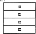
- FIG. 1 illustrates an inverted-structured organic solar cell, one example of the organic solar cell according to one embodiment of the present specification.
- a buffer layer (301) is formed between a first electrode (101) and a photoactive layer (401), and a second electrode (201) is provided on the photoactive layer (401).
- the inverted structure may mean forming a cathode on a substrate.
- the first electrode formed on a substrate may be a cathode when the organic solar cell has an inverted structure.
- the first electrode may be a transparent electrode or a translucent electrode.
- the first electrode When the first electrode is a transparent electrode, it may be a transparent conductive oxide, and in this case, the first electrode may be a conductive oxide such as indium tin oxide (ITO) or indium zinc oxide (IZO). Furthermore, the first electrode may be a translucent electrode. When the first electrode is a translucent electrode, it may be prepared with a translucent metal such as Ag, Au, Mg, Ca or alloys thereof. When using a translucent metal as the first electrode, the organic solar cell may have a microcavity structure.
- ITO indium tin oxide
- IZO indium zinc oxide
- the first electrode may be a translucent electrode.
- the first electrode When the first electrode is a translucent electrode, it may be prepared with a translucent metal such as Ag, Au, Mg, Ca or alloys thereof.
- the organic solar cell When using a translucent metal as the first electrode, the organic solar cell may have a microcavity structure.
- the first electrode of the present specification is a transparent conductive oxide
- the first electrode may include, in addition to glass and a quartz plate, those doping a material having conductivity on a flexible and transparent material such as plastic including polyethylene terephthalate (PET), polyethylene naphthalate (PEN), polypropylene (PP), polyimide (PI), polycarbonate (PC), polystyrene (PS), polyoxymethylene (POM), an acrylonitrile styrene (AS) resin (copolymer), an acrylonitrile butadiene styrene (ABS) resin (copolymer), triacetyl cellulose (TAC), polyarylate (PAR) and the like.
- plastic including polyethylene terephthalate (PET), polyethylene naphthalate (PEN), polypropylene (PP), polyimide (PI), polycarbonate (PC), polystyrene (PS), polyoxymethylene (POM), an acrylonitrile styrene (
- ITO indium tin oxide
- FTO fluorine-doped tin oxide
- AZO aluminum-doped zinc oxide
- IZO indium zinc oxide
- ZnO-Ga 2 O 3 ZnO-Al 2 O 3
- antimony tin oxide (ATO) and the like may be included, and more specifically, ITO may be included.
- Another embodiment may provide an organic solar cell having normal structure in which the first electrode is an anode and the second electrode is a cathode, and the buffer layer is provided between the second electrode and the photoactive layer.
- FIG. 2 illustrates a normal-structured organic solar cell, one example of the organic solar cell according to one embodiment of the present specification.
- a buffer layer (301) is formed between a second electrode (201) and a photoactive layer (401), and a first electrode (101) is provided on the photoactive layer (401).
- the normal structure may mean forming an anode on a substrate.
- the first electrode formed on a substrate may be an anode when the organic solar cell has a normal structure.
- the second electrode may be a metal electrode.
- the second electrode of the present specification is a metal electrode
- the second electrode may include one, two or more types selected from the group consisting of silver (Ag), aluminum (Al), platinum (Pt), tungsten (W), copper (Cu), molybdenum (Mo), gold (Au), nickel (Ni) and palladium (Pd).
- the metal electrode may be silver (Ag).
- the organic solar cell may further include a substrate.
- the substrate may be provided below the first electrode.
- substrates having excellent transparency, surface smoothness, handling easiness and water resistance may be used as the substrate.
- a glass substrate, a thin film glass substrate or a transparent plastic substrate may be used.
- plastic substrate films such as polyethylene terephthalate (PET), polyethylene naphthalate (PEN), polyether ether ketone (PEEK) and polyimide (PI) may be included in a monolayer or multilayer form.
- PET polyethylene terephthalate
- PEN polyethylene naphthalate
- PEEK polyether ether ketone
- PI polyimide
- the substrate is not limited thereto, and substrates commonly used in an organic solar cell may be used.
- the forming of a first electrode and/or a second electrode may include cleaning a patterned ITO substrate consecutively with a cleaning agent, acetone and isopropanol (IPA), then drying the substrate on a heating plate for 1 minute to 30 minutes at 100°C to 250°C, specifically for 10 minutes at 250°C, for removing moisture, and then modifying the substrate surface to be hydrophilic when the substrate is completely cleaned.
- IPA acetone and isopropanol
- Preprocessing technologies for this may include a) a surface oxidation method using parallel plate discharge, b) a method of oxidizing the surface through ozone generated by UV rays in a vacuum, and c) an oxidation method using the oxygen radicals generated by plasma.
- the junctional surface potential may be maintained at a level suitable for the surface potential of a hole injection layer, a polymer thin film may be readily formed on the ITO substrate, the quality of the thin film may be improved.
- One of the methods described above is selected depending on the condition of the substrate, however, no matter which method is used, it is commonly preferred to prevent the leave of oxygen on the substrate surface and to suppress the remaining of moisture and organic materials as much as possible in order to expect practical effects of the preprocessing.
- a method of oxidizing the surface through ozone generated by UV may be used as the method of oxidizing the substrate.
- the patterned ITO substrate may be fully dried by baking the patterned ITO substrate on a hot plate after being ultrasonic cleaned, and the patterned ITO substrate is introduced into a chamber and then cleaned by ozone generated by reacting oxygen gas with UV light using a UV lamp.
- the method of surface modification of the patterned ITO substrate in the present disclosure is not particularly limited, and any method oxidizing a substrate may be used.
- the copolymer was formed by the following Reaction Formula 1.
- Chlorobenzene (15 ml), 2,6-bis(trimethyltin)-4,8-bis(2-ethylhexyl-2-thienyl)-benzo[1,2-b:4,5-b']dithiophene (0.7 g, 0.7738 mmol), 2,5-bis(trimethylstannyl)thiophene (0.3171 g, 0.7738 mmol), 1,3-dibromo-5-dodecylthieno[3,4-c]pyrrole-4,6-dione (0.7418 g, 1.548 mmol), tris(dibenzylideneacetone)dipalladium(0) (Pd 2 (dba) 3 , 28 mg), tri-(o-tolyl)phosphine (37 mg) were placed in a microwave reactor vial, and reacted for 1 hour under a 170°C condition.
- the mixture was cooled to room temperature, methanol was poured thereinto, and then solids were filtered and then Soxhlet extracted using methanol, acetone, hexane and chloroform. The chloroform portion was precipitated again in methanol to filter solids.
- PEI and 1-butanol were mixed in a mass ratio of 1:499, and stored for 24 hours or longer.
- a photoactive layer solution was prepared to have an approximately 3 wt% concentration employing a donor and an acceptor (CF, CB, ODCB or mixed solution of two or more thereof) in a 1:2 ratio.
- the photoactive layer solution according to one embodiment of the present specification was prepared by adding the PEI solution to the photoactive layer solution prepared above.
- the structure (ITO /125:PC61BM:PEI/MoO3/Ag) prepared according to one embodiment of the present specification 1,2,4-trichlorobenzene was included in 3% by weight, and a device was manufactured by coating while maintaining the temperature of the substrate and the temperature of the photoactive layer solution identically at 40°C.
- a device was manufactured in the same manner as in Example 2 except for the step of coating while maintaining the temperature identically at 40°C.
- a device was manufactured in the same manner as in Example 2 except that 1,2,4-trichlorobenzene was included in 10% by weight.
- a device was manufactured in a general structure (ITO/ZnO/ 125:PC61BM/MoO3/Ag) used in the art.
- a device was manufactured without 1,2,4-trichlorobenzene and a process of heat treating the substrate and the solution in the structure (ITO/125:PC61BM:PEI/MoO3/Ag) according to one embodiment of the present specification.
- Example 2 4.833 2.516 0.579 7.03 Comparative Example 1 4.8 2.622 0.48 6.04 Comparative Example 2 3.79 1.66 0.38 2.39 Comparative Example 3 4.862 2.5 0.560 6.81 Comparative Example 4 3.891 2.334 0.375 3.41
- the V oc means an open voltage
- the J sc means a short-circuit current
- the FF means a fill factor
- the PCE means power conversion efficiency.
- the open voltage and the short-circuit current are each an x-axis and a ⁇ -axis intercept in the four quadrants of a voltage-current density curve, and as these two values increase, organic solar cell efficiency is enhanced.
- the fill factor is a value dividing the rectangle area that may be drawn inside the curve by the product of the short-circuit current and the open voltage. The power conversion efficiency may be obtained when these three values are divided by the intensity of irradiated light, and target effects are obtained as the value is higher.
- the organic solar cells according to the examples exhibited superior efficiency when using 1,2,4-trichlorobenzene as the phase separation solvent and setting the temperature condition at a certain temperature compared to the organic solar cells according to the comparative examples lacking these conditions.
- the solar cells according to the examples had enhanced current density by enhancing a light absorption ability of the photoactive layer due to a light concentrating effect of Ag nanoparticles, and had a high fill factor since conductivity of the buffer layer was enhanced by Ag nanoparticles, and a decrease in the current density caused by voltage was smaller.
Landscapes
- Engineering & Computer Science (AREA)
- Manufacturing & Machinery (AREA)
- Physics & Mathematics (AREA)
- Electromagnetism (AREA)
- Photovoltaic Devices (AREA)
Abstract
Description
- The present specification claims priority to and the benefits of Korean Patent Application No.
10-2016-0029651 - The present specification relates to a method for manufacturing an organic solar cell, and an organic solar cell manufactured using the same.
- According to an energy review material published by the NREL, a US National Laboratory, energy sources that are currently used mainly are petroleum, coal and gas. These energy sources amount to 80% of energy sources used in total. However, depletion of petroleum and coal energy has gradually become a big problem currently, and an increase in the emission of carbon dioxide and other greenhouse gases into the air is generating increasingly serious problems. In contrast, the use of renewable energy that is non-polluting green energy is yet about 2% of the total energy source. Thus, concerns about resolving energy source problems have become a motivation for expediting studies on developing new renewable energy. Among the new renewable energy sources such as wind, water and the sun, solar energy has received most attention. Solar cells using solar energy produce less pollution, are limitless in resources and have a semi-permanent lifetime, and therefore, are expected as an energy source capable of resolving future energy problems.
- An organic solar cell is a device capable of directly converting solar energy to electric energy by applying a photovoltaic effect. Solar cells are divided into inorganic solar cells and organic solar cells depending on the materials forming a thin film. Typical solar cells are fabricated using a p-n junction by doping crystalline silicon (Si), an inorganic semiconductor. Electrons and holes generated by light absorption spread to p-n junction points, are accelerated by the electric field, and migrate to an electrode. Power conversion efficiency of this process is defined as a ratio of power given to an external circuit and solar power put into a solar cell, and the ratio has been accomplished up to approximately 24% when measured under a currently standardized hypothetical solar irradiation condition. However, existing inorganic solar cells already have limits in economic feasibility and material supplies, and therefore, organic solar cells that are readily processed, inexpensive and have various functions have been highly favored as a long-term alternative energy source.
- As for early organic solar cells, the group of Professor Heeger at UCSB of the US has initiatively led the technology development. Monomolecular organic materials or polymer materials used in technologies of a two-step manufacturing process for forming each of a buffer layer and a photoactive layer of an organic solar cell have advantages in that they are readily and quickly used in low-priced and large area processes.
- However, a method of manufacturing a buffer layer and a photoactive layer in a one-step process through self-phase separation has a problem of not usable in a large-area module solar cell that is not a unit device since constituents of the buffer layer are non-conductors and an ultrathin film needs to be formed. Accordingly, development of technologies capable of being used in a large-area module solar cell while manufacturing a buffer layer and a photoactive layer in a one-step process has been required.
- The present specification is directed to providing a method for manufacturing a highly efficient organic solar cell through a self-phase separation method usable in a large-area module.
- One embodiment of the present specification provides a method for manufacturing an organic solar cell including preparing a first electrode; preparing a solution including a solvent, a buffer material and a photoactive material; forming a buffer layer and a photoactive layer through coating of applying the solution on the first electrode and heat treating the result; and forming a second electrode on the photoactive layer, wherein the solvent includes a phase separation solvent for self-phase separation of the buffer layer and the photoactive layer.
- Another embodiment of the present specification provides an organic solar cell manufactured using the method for manufacturing an organic solar cell of the present disclosure.
- According to a solar cell according to one embodiment of the present specification, self-phase separation of a buffer layer and a photoactive layer can smoothly occur.
- *15 According to the solar cell according to one embodiment of the present specification, the smooth self-phase separation of the buffer layer and the photoactive layer can be used in a large-area module.
- According to the solar cell according to one embodiment of the present specification, large photoconversion efficiency can be obtained even when the smooth self-phase separation of the buffer layer and the photoactive layer is used in the large-area module by concentrating light with the photoactive layer.
- According to a solar cell according to one embodiment of the present specification, the buffer layer and the photoactive layer can be formed in the large-area module in one step, and shorter process time and process cost savings can be obtained.
-
-
FIG. 1 illustrates a sectional diagram of an inverted-structured organic solar cell according to one embodiment of the present specification. -
FIG. 2 illustrates a sectional diagram of a normal-structured organic solar cell according to one embodiment of the present specification. - Hereinafter, the present specification will be described in more detail.
- In the present specification, a description of a certain member being placed "on" another member includes not only a case of the one member adjoining the another member but a case of still another member being present between the two members.
- In the present specification, a description of a certain part "including" certain constituents means capable of further including other constituents, and does not exclude other constituents unless particularly stated on the contrary.
- One embodiment of the present specification provides a method for manufacturing an organic solar cell including preparing a first electrode; preparing a solution including a solvent, a buffer material and a photoactive material; forming a buffer layer and a photoactive layer through coating of applying the solution on the first electrode and heat treating the result; and forming a second electrode on the photoactive layer, wherein the solvent includes a phase separation solvent for self-phase separation of the buffer layer and the photoactive layer.
- In the present specification, the buffer material is a material for forming a buffer layer, and the buffer material may include one or more types selected from the group consisting of metal salts, metal oxides and non-conjugated polyelectrolytes (NPE).
- The metal salt of the present specification is capable of forming a buffer layer with no impurities such as a reducing agent or a surfactant through a process of forming metal particles by being reduced with heat treatment, and although not particularly limited in the type, may include one or more types selected from the group consisting of Ag metal salts, Au metal salts, Al metal salts, Cu metal salts, W metal salts and Pt metal salts.
- According to one embodiment of the present specification, the Ag metal salt may include one or more selected from the group consisting of AgCl, AgNO3 and AgI. However, the Ag metal salt is not limited thereto.
- *27According to one embodiment of the present specification, the Au metal salt may include one or more selected from the group consisting of HAuCl4, AuCl and AuCl3. However, the Au metal salt is not limited thereto.
- According to one embodiment of the present specification, the Cu metal salt may include one or more selected from the group consisting of CuI, CuF3 and CuNO3. However, the Cu metal salt is not limited thereto.
- According to one embodiment of the present specification, the Pt metal salt may include one or more selected from the group consisting of PtCl2, PtCl4, PtBr2 and Pt(C5H7O2)2. However, the Pt metal salt is not limited thereto.
- The metal oxide of the present specification may perform a role of a conductive oxide in the buffer layer, and although not particularly limited in the type, may be one or more types selected from the group consisting of molybdenum oxide (MoO3), vanadium oxide (VOx), nickel oxide (NiO), zinc oxide (ZnO); titanium oxide (TiO2); zirconium oxide (ZrO2); tantalum oxide (Ta2O3) ; cesium oxide (Cs2CO3) ; magnesium oxide (MgO) ; hafnium oxide (HfO2); tungsten oxide (WO3); and zinc oxide (ZnO) doped with aluminum (Al) or gallium (Ga).
- According to one embodiment of the present specification, the non-conjugated polyelectrolyte may perform a role of transferring electrons in the buffer layer, and although not particularly limited as long as it is capable of transferring electrons, may include one or more types selected from the group consisting of polyethyleneimine (PEI), polyethyleneimine ethoxylate (PEIE) and polyallylamine (PAA).
- According to one embodiment of the present specification, the photoactive material is for forming a photoactive layer, and the photoactive material may include an electron donor material and an electron acceptor material. In the present specification, the photoactive material may mean the electron donor material and the electron acceptor material.
- In one embodiment of the present specification, the electron donor material and the electron acceptor material may have a mass ratio of 1:10 to 10:1. Specifically, the electron acceptor material and the electron donor material of the present specification may have a mass ratio of 1:0.5 to 1:5.
- According to one embodiment of the present specification, the electron donor material may include at least one type of electron donor; or a polymer of at least one type of electron acceptor and at least one type of electron donor. The electron donor material may include at least one type of electron donor. In addition, the electron donor material includes a polymer of at least one type of electron acceptor and at least one type of electron donor.
- Specifically, the electron donor material may be various polymer materials and monomer materials such as thiophene-based, fluorene-based or carbazole based starting with poly[2-methoxy-5-(2'-ethyl-hexyloxy)-1,4-phenylene vinylene] (MEH-PPV) .
- Specifically, the monomer material may include one or more types of materials selected from the group consisting of copper (II) phthalocyanine, zinc phthalocyanine, tris[4-(5-dicyanomethylidenemethyl-2-thienyl)phenyl] amine, 2,4-bis[4-(N,N-dibenzylamino)-2,6-dihydroxyphenyl] squaraine, benz[b]anthracene, and pentacene.
- Specifically, the polymer material may include one or more types of materials selected from the group consisting of poly 3-hexyl thiophene (P3HT), poly[N-9'-heptadecanyl-2,7-carbazole-alt-5,5-(4'-7'-di-2-thienyl-2'1',3'-benzothiadiazole)] (PCDTBT), poly[2,6-(4,4-bis-(2,ethylhexyl)-4H-cyclopenta[2,1-b;3,4-b']dithiophene)-alt-4,7-(2,1,3-benzothiadiazole)] (PCPDTBT), poly[2,7-(9,9-dioctyl-fluorene)-alt-5,5-(4,7-di-2-thienyl-2,1,3-benzothiadiazole)] (PFO-DBT), poly[[4,8-bis[(2-ethylhexyl)oxy]benzo[1,2-b:4,5-b']dithiophene-2,6-diyl] [3-fluoro-2-[(2-ethylhexyl)carbonyl] thieno[3,4-b]thiophenediyl]] (PTB7), and poly[2,7-(9,9-dioctyl-dibenzosilole)-alt-4,7-bis(thiophen-2-yl)benzo-2,1,3-thiadiazole] (PSiF-DBT).
- According to one embodiment of the present specification, the photoactive material may include the following copolymer.

- l is a mole fraction, and 0<l<1,
- m is a mole fraction, and 0<m<1,
- l+m=1, and
- o is an integer of 0<o<1,000.
- In one embodiment of the present specification, 1 is 0.5.
- In another embodiment, m is 0.5.
- In one embodiment of the present specification, the copolymer may be synthesized by the examples to describe later.
- In one embodiment of the present specification, an end group of the copolymer may be a heterocyclic group or an aryl group.
- In one embodiment of the present specification, an end group of the copolymer may be a 4-(trifluoromethyl)phenyl group.
- According to one embodiment of the present specification, the copolymer may have a number average molecular weight of 500 g/mol to 1,000,000 g/mol. Specifically, the copolymer may have a number average molecular weight of 10,000 g/mol to 100,000 g/mol. In addition, in one embodiment of the present specification, the copolymer has a number average molecular weight of 30,000 g/mol to 70,000 g/mol.
- According to one embodiment of the present specification, the copolymer may have molecular weight distribution of 1 mol to 100 mol. Specifically, the copolymer may have molecular weight distribution of 1 to 3.
- As the molecular weight distribution decreases and the number average molecular weight increases, electrical properties and mechanical properties become more favorable.
- In addition, the number average molecular weight may be 100,000 g/mol or less in order to have solubility at a certain level or higher and facilitate solution coating.
- According to one embodiment of the present specification, the compound may be included as an electron donor in the photoactive material.
- According to one embodiment of the present specification, the forming of a buffer layer and a photoactive layer may be by self-phase separation.
- The buffer layer may mean a layer transferring "holes" or "electrons". In addition, the buffer layer may be an electron transfer layer, a charge transfer layer or a hole transfer layer.
- In the photoactive layer, the electron donor material forms excitons pairing electrons and holes, and the excitons are separated into electrons and holes at an interface of the electron donor/electron acceptor. The separated electrons and holes migrate to the electron donor material and the electron acceptor material, respectively, and by these being collected in a first electrode and a second electrode, respectively, an organic solar cell may be externally used as electric energy.
- In addition, in one embodiment of the present specification, the photoactive layer may have a bulk heterojunction structure or a bi-layer junction structure. The bulk heterojunction structure may be a bulk heterojunction (BHJ) type, and the bi-layer junction structure may be a bi-layer junction type.
- The self-phase separation means two or more groups having different properties under a certain condition being separated into each group, and in the present specification, the self-phase separation may be induced through heat treating the solution including a solvent, a buffer material and a photoactive material.
- According to one embodiment of the present specification, the coating may be by any one selected from the group consisting of bar coating, slot die coating, doctor blade coating, screen coating and spin coating. Specifically, the coating may be by bar coating.
- In a unit device that is a small-area module of 1 cm2 or less, a coating method such as spin coating may be used, however, this method may not be used in large-area coating, and has a problem in that patterning, an essential condition to manufacture a device, may not be performed. However, the solution according to one embodiment of the present specification may also be used in a large-area module, and therefore, the bar coating method usable in a large-area module may be used, and coating efficiency may be enhanced therefrom.
- According to one embodiment of the present specification, the heat treatment temperature may be from 20°C to 70°C. More specifically, the heat treatment temperature may be from 30°C to 40°C.
- According to one embodiment of the present specification, the solvent may include a phase separation solvent in order to enhance an effect of inducing self-phase separation of the buffer layer and the photoactive layer.
- The type of the phase separation solvent is not particularly limited as long as it is a material inducing self-phase separation, however, the solvent may be a material having a boiling point of 200°C to 230°C and density of 1 g/cm3 to 5 g/cm3. When a boiling point and density of the phase separation solvent are outside the above-mentioned range, phase separation may not be induced, which requires an additional process, and as a result, process efficiency may decrease.
- Specific examples of the phase separation solvent are not particularly limited, but may be 1,2,4-trichlorobenzene (TCB).
- In addition, the phase separation solvent may be included in 2% by weight to 8% by weight with respect to 100% by weight of the solution. Specifically, the phase separation solvent may be included in 2% by weight to 5% by weight with respect to 100% by weight of the solution. More specifically, the phase separation solvent may be included in 3% by weight with respect to 100% by weight of the solution.
- One embodiment of the present specification may provide an organic solar cell manufactured using the method for manufacturing an organic solar cell of the present specification.
- In addition, one embodiment of the present specification may provide an organic solar cell having an inverted structure in which the first electrode is a cathode and the second electrode is an anode, and the buffer layer is provided between the first electrode and the photoactive layer.
-
FIG. 1 illustrates an inverted-structured organic solar cell, one example of the organic solar cell according to one embodiment of the present specification. When referring toFIG. 1 , a buffer layer (301) is formed between a first electrode (101) and a photoactive layer (401), and a second electrode (201) is provided on the photoactive layer (401). - The inverted structure may mean forming a cathode on a substrate. Specifically, according to one embodiment of the present specification, the first electrode formed on a substrate may be a cathode when the organic solar cell has an inverted structure. In this case, the first electrode may be a transparent electrode or a translucent electrode.
- When the first electrode is a transparent electrode, it may be a transparent conductive oxide, and in this case, the first electrode may be a conductive oxide such as indium tin oxide (ITO) or indium zinc oxide (IZO). Furthermore, the first electrode may be a translucent electrode. When the first electrode is a translucent electrode, it may be prepared with a translucent metal such as Ag, Au, Mg, Ca or alloys thereof. When using a translucent metal as the first electrode, the organic solar cell may have a microcavity structure.
- When the first electrode of the present specification is a transparent conductive oxide, the first electrode may include, in addition to glass and a quartz plate, those doping a material having conductivity on a flexible and transparent material such as plastic including polyethylene terephthalate (PET), polyethylene naphthalate (PEN), polypropylene (PP), polyimide (PI), polycarbonate (PC), polystyrene (PS), polyoxymethylene (POM), an acrylonitrile styrene (AS) resin (copolymer), an acrylonitrile butadiene styrene (ABS) resin (copolymer), triacetyl cellulose (TAC), polyarylate (PAR) and the like. Specifically, indium tin oxide (ITO), fluorine-doped tin oxide (FTO), aluminum-doped zinc oxide (AZO), indium zinc oxide (IZO), ZnO-Ga2O3, ZnO-Al2O3, antimony tin oxide (ATO) and the like may be included, and more specifically, ITO may be included.
- *72 The inverted-structured organic solar cell of the present specification may mean an organic solar cell in which an anode and a cathode of an organic solar cell having a general structure are formed in a reverse direction. An Al layer used in an organic solar cell having a general structure is very vulnerable to an oxidation reaction in the air, and has a limit in commercializing through a printing process since preparing in an ink form is difficult. However, the organic solar cell of the present specification having a structure in a reverse direction is capable of using Ag instead of Al, and therefore, is stable for an oxidation reaction compared to an organic solar cell having a general structure, and an Ag ink is readily prepared, which is advantageous in commercializing through a printing process.
- Another embodiment may provide an organic solar cell having normal structure in which the first electrode is an anode and the second electrode is a cathode, and the buffer layer is provided between the second electrode and the photoactive layer.
-
FIG. 2 illustrates a normal-structured organic solar cell, one example of the organic solar cell according to one embodiment of the present specification. When referring toFIG. 2 , a buffer layer (301) is formed between a second electrode (201) and a photoactive layer (401), and a first electrode (101) is provided on the photoactive layer (401). - The normal structure may mean forming an anode on a substrate. Specifically, according to one embodiment of the present specification, the first electrode formed on a substrate may be an anode when the organic solar cell has a normal structure. In this case, the second electrode may be a metal electrode.
- When the second electrode of the present specification is a metal electrode, the second electrode may include one, two or more types selected from the group consisting of silver (Ag), aluminum (Al), platinum (Pt), tungsten (W), copper (Cu), molybdenum (Mo), gold (Au), nickel (Ni) and palladium (Pd). Even more specifically, the metal electrode may be silver (Ag).
- According to one embodiment of the present specification, the organic solar cell may further include a substrate. Specifically, the substrate may be provided below the first electrode.
- According to one embodiment of the present specification, substrates having excellent transparency, surface smoothness, handling easiness and water resistance may be used as the substrate. Specifically, a glass substrate, a thin film glass substrate or a transparent plastic substrate may be used. As the plastic substrate, films such as polyethylene terephthalate (PET), polyethylene naphthalate (PEN), polyether ether ketone (PEEK) and polyimide (PI) may be included in a monolayer or multilayer form. However, the substrate is not limited thereto, and substrates commonly used in an organic solar cell may be used.
- In one embodiment of the present specification, the forming of a first electrode and/or a second electrode may include cleaning a patterned ITO substrate consecutively with a cleaning agent, acetone and isopropanol (IPA), then drying the substrate on a heating plate for 1 minute to 30 minutes at 100°C to 250°C, specifically for 10 minutes at 250°C, for removing moisture, and then modifying the substrate surface to be hydrophilic when the substrate is completely cleaned. Preprocessing technologies for this may include a) a surface oxidation method using parallel plate discharge, b) a method of oxidizing the surface through ozone generated by UV rays in a vacuum, and c) an oxidation method using the oxygen radicals generated by plasma. Through the surface modification such as above, the junctional surface potential may be maintained at a level suitable for the surface potential of a hole injection layer, a polymer thin film may be readily formed on the ITO substrate, the quality of the thin film may be improved. One of the methods described above is selected depending on the condition of the substrate, however, no matter which method is used, it is commonly preferred to prevent the leave of oxygen on the substrate surface and to suppress the remaining of moisture and organic materials as much as possible in order to expect practical effects of the preprocessing.
- According to one embodiment of the present specification, a method of oxidizing the surface through ozone generated by UV may be used as the method of oxidizing the substrate. In this case, the patterned ITO substrate may be fully dried by baking the patterned ITO substrate on a hot plate after being ultrasonic cleaned, and the patterned ITO substrate is introduced into a chamber and then cleaned by ozone generated by reacting oxygen gas with UV light using a UV lamp. However, the method of surface modification of the patterned ITO substrate in the present disclosure is not particularly limited, and any method oxidizing a substrate may be used.
- Hereinafter, the present specification will be described in detail with reference to examples in order to specifically describe the present specification. However, examples according to the present specification may be modified to various different forms, and the scope of the present specification is not construed as being limited to the examples described below. Examples of the present specification are provided in order to more fully describe the present specification to those having average knowledge in the art.
- In order to synthesize a copolymer included in a photoactive material according to one embodiment of the present specification, the copolymer was formed by the following Reaction Formula 1.


- Chlorobenzene (15 ml), 2,6-bis(trimethyltin)-4,8-bis(2-ethylhexyl-2-thienyl)-benzo[1,2-b:4,5-b']dithiophene (0.7 g, 0.7738 mmol), 2,5-bis(trimethylstannyl)thiophene (0.3171 g, 0.7738 mmol), 1,3-dibromo-5-dodecylthieno[3,4-c]pyrrole-4,6-dione (0.7418 g, 1.548 mmol), tris(dibenzylideneacetone)dipalladium(0) (Pd2(dba)3, 28 mg), tri-(o-tolyl)phosphine (37 mg) were placed in a microwave reactor vial, and reacted for 1 hour under a 170°C condition. The mixture was cooled to room temperature, methanol was poured thereinto, and then solids were filtered and then Soxhlet extracted using methanol, acetone, hexane and chloroform. The chloroform portion was precipitated again in methanol to filter solids.
- In order to prepare a PEI solution, PEI and 1-butanol were mixed in a mass ratio of 1:499, and stored for 24 hours or longer. A photoactive layer solution was prepared to have an approximately 3 wt% concentration employing a donor and an acceptor (CF, CB, ODCB or mixed solution of two or more thereof) in a 1:2 ratio.
- The photoactive layer solution according to one embodiment of the present specification was prepared by adding the PEI solution to the photoactive layer solution prepared above. In the structure (ITO /125:PC61BM:PEI/MoO3/Ag) prepared according to one embodiment of the present specification, 1,2,4-trichlorobenzene was included in 3% by weight, and a device was manufactured by coating while maintaining the temperature of the substrate and the temperature of the photoactive layer solution identically at 40°C.
- A device was manufactured in the same manner as in Example 2 except for the step of coating while maintaining the temperature identically at 40°C.
- A device was manufactured in the same manner as in Example 2 except that 1,2,4-trichlorobenzene was included in 10% by weight.
- A device was manufactured in a general structure (ITO/ZnO/ 125:PC61BM/MoO3/Ag) used in the art.
- A device was manufactured without 1,2,4-trichlorobenzene and a process of heat treating the substrate and the solution in the structure (ITO/125:PC61BM:PEI/MoO3/Ag) according to one embodiment of the present specification.
- Properties of the organic solar cells manufactured in the examples and the comparative examples are shown in the following Table 1.
- The module size of the organic solar cells was 9 cmx1.5 cm=13.5 cm2, which is a large-area module instead of an existing small-area module of 1 cm2 or less.
[Table 1] Voc (V) Jsc (mA/cm2) FF PCE (%) Example 2 4.833 2.516 0.579 7.03 Comparative Example 1 4.8 2.622 0.48 6.04 Comparative Example 2 3.79 1.66 0.38 2.39 Comparative Example 3 4.862 2.5 0.560 6.81 Comparative Example 4 3.891 2.334 0.375 3.41 - In the present specification, the Voc means an open voltage, the Jsc means a short-circuit current, the FF means a fill factor, and the PCE means power conversion efficiency. The open voltage and the short-circuit current are each an x-axis and a γ-axis intercept in the four quadrants of a voltage-current density curve, and as these two values increase, organic solar cell efficiency is enhanced. In addition, the fill factor is a value dividing the rectangle area that may be drawn inside the curve by the product of the short-circuit current and the open voltage. The power conversion efficiency may be obtained when these three values are divided by the intensity of irradiated light, and target effects are obtained as the value is higher.
- As can be seen from Table 1, the organic solar cells according to the examples exhibited superior efficiency when using 1,2,4-trichlorobenzene as the phase separation solvent and setting the temperature condition at a certain temperature compared to the organic solar cells according to the comparative examples lacking these conditions.
- As can be seen from Table 1, it was identified that the solar cells according to the examples had enhanced current density by enhancing a light absorption ability of the photoactive layer due to a light concentrating effect of Ag nanoparticles, and had a high fill factor since conductivity of the buffer layer was enhanced by Ag nanoparticles, and a decrease in the current density caused by voltage was smaller.
Claims (15)
- A method for manufacturing an organic solar cell comprising:preparing a first electrode;preparing a solution including a solvent, a buffer material and a photoactive material;forming a buffer layer and a photoactive layer through coating of applying the solution on the first electrode and heat treating the result; andforming a second electrode on the photoactive layer,wherein the solvent includes a phase separation solvent for self-phase separation of the buffer layer and the photoactive layer.
- The method for manufacturing an organic solar cell of Claim 1, wherein the buffer material includes one or more types selected from the group consisting of metal salts, metal oxides and non-conjugated polyelectrolytes (NPE).
- The method for manufacturing an organic solar cell of Claim 2, wherein the metal salt includes one or more types selected from the group consisting of Ag metal salts, Au metal salts, Al metal salts, Cu metal salts, W metal salts and Pt metal salts.
- The method for manufacturing an organic solar cell of Claim 2, wherein the metal oxide is one or more types selected from the group consisting of molybdenum oxide (MoO3), vanadium oxide (VOx), nickel oxide (NiO), zinc oxide (ZnO); titanium oxide (TiO2) ; zirconium oxide (ZrO2) ; tantalum oxide (Ta2O3); cesium oxide (Cs2CO3); magnesium oxide (MgO); hafnium oxide (HfO2) ; tungsten oxide (WO3); and zinc oxide (ZnO) doped with aluminum (Al) or gallium (Ga).
- The method for manufacturing an organic solar cell of Claim 2, wherein the non-conjugated polyelectrolyte includes one or more types selected from the group consisting of polyethyleneimine (PEI), polyethyleneimine ethoxylate (PEIE) and polyallylamine (PAA).
- The method for manufacturing an organic solar cell of Claim 1, wherein the photoactive material includes the following copolymer:
 l is a mole fraction, and 0<l<1;m is a mole fraction, and 0<m<1;l+m=1; ando is an integer of 0<o<1,000.
 - The method for manufacturing an organic solar cell of Claim 1, wherein the forming of a buffer layer and a photoactive layer is by self-phase separation.
- The method for manufacturing an organic solar cell of Claim 1, wherein the coating is any one selected from the group consisting of bar coating, slot die coating or doctor blade coating.
- The method for manufacturing an organic solar cell of Claim 1, wherein a temperature of the heat treatment is from 20°C to 70°C.
- The method for manufacturing an organic solar cell of Claim 1, wherein the phase separation solvent has a boiling point of 200°C to 230°C and density of 1 g/cm3 to 5 g/cm3.
- The method for manufacturing an organic solar cell of Claim 1, wherein the phase separation solvent is 1,2,4-trichlorobenzene (TCB).
- The method for manufacturing an organic solar cell of Claim 1, wherein the phase separation solvent is included in 2% by weight to 8% by weight with respect to 100% by weight of the solution.
- An organic solar cell manufactured using the method of any one of Claims 1 to 12.
- The organic solar cell of Claim 13, which has an inverted structure in which the first electrode is a cathode and the second electrode is an anode, and the buffer layer is provided between the first electrode and the photoactive layer.
- The organic solar cell of Claim 13, which has a normal structure in which the first electrode is an anode and the second electrode is a cathode, and the buffer layer is provided between the second electrode and the photoactive layer.
Applications Claiming Priority (2)
| Application Number | Priority Date | Filing Date | Title |
|---|---|---|---|
| KR1020160029651A KR102116162B1 (en) | 2016-03-11 | 2016-03-11 | Organic solar cell and method for manufacturing the same |
| PCT/KR2017/002658 WO2017155362A1 (en) | 2016-03-11 | 2017-03-13 | Organic solar cell and method for manufacturing same |
Publications (3)
| Publication Number | Publication Date |
|---|---|
| EP3410507A1 true EP3410507A1 (en) | 2018-12-05 |
| EP3410507A4 EP3410507A4 (en) | 2019-03-27 |
| EP3410507B1 EP3410507B1 (en) | 2022-08-24 |
Family
ID=59789655
Family Applications (1)
| Application Number | Title | Priority Date | Filing Date |
|---|---|---|---|
| EP17763622.2A Active EP3410507B1 (en) | 2016-03-11 | 2017-03-13 | Organic solar cell and method for manufacturing same |
Country Status (6)
| Country | Link |
|---|---|
| US (1) | US10672985B2 (en) |
| EP (1) | EP3410507B1 (en) |
| JP (1) | JP6791256B2 (en) |
| KR (1) | KR102116162B1 (en) |
| CN (1) | CN108780847B (en) |
| WO (1) | WO2017155362A1 (en) |
Cited By (1)
| Publication number | Priority date | Publication date | Assignee | Title |
|---|---|---|---|---|
| CN111628085A (en) * | 2020-06-08 | 2020-09-04 | 遵义师范学院 | A kind of organic solar cell based on double electron transport layer and preparation method thereof |
Families Citing this family (1)
| Publication number | Priority date | Publication date | Assignee | Title |
|---|---|---|---|---|
| CN111244285B (en) * | 2020-01-20 | 2023-04-18 | 遵义师范学院 | Double-layer electron transmission layer for solar cell and application thereof |
Family Cites Families (13)
| Publication number | Priority date | Publication date | Assignee | Title |
|---|---|---|---|---|
| US5331183A (en) | 1992-08-17 | 1994-07-19 | The Regents Of The University Of California | Conjugated polymer - acceptor heterojunctions; diodes, photodiodes, and photovoltaic cells |
| TWI497740B (en) * | 2009-10-05 | 2015-08-21 | Univ Nat Chiao Tung | Polymer solar battery and manufacturing method thereof |
| US9608225B2 (en) * | 2010-01-21 | 2017-03-28 | Samsung Electronics Co., Ltd. | Light emitting device and method of fabricating the same |
| KR101175178B1 (en) * | 2011-03-16 | 2012-08-20 | 연세대학교 산학협력단 | Method of manufacturing bulk heterojunction solar cell capable of improving power conversion efficiency and the bulk heterojunction solar cell |
| CN102623639B (en) * | 2012-04-10 | 2014-10-08 | 合肥工业大学 | Method for manufacturing organic thin film transistor realizing patterning and automatic-modification interface in one step |
| JP2014029904A (en) * | 2012-07-31 | 2014-02-13 | Fuji Electric Co Ltd | Organic thin-film solar cell and method of manufacturing the same |
| CN102891259B (en) * | 2012-09-28 | 2017-11-07 | 北京大学 | Donor organic solar batteries being separated vertical with acceptor and preparation method thereof |
| KR101587895B1 (en) * | 2013-12-24 | 2016-01-22 | 광주과학기술원 | Inverted organic electronic device and method for manufacturing the same |
| TWI550929B (en) * | 2014-02-14 | 2016-09-21 | Lg化學股份有限公司 | Copolymer and organic solar cell containing same |
| KR101679965B1 (en) * | 2014-04-30 | 2016-11-28 | 주식회사 엘지화학 | Solar cell and method for manufacturing the same |
| CN106463628B (en) * | 2014-04-30 | 2018-11-09 | 株式会社Lg化学 | Organic solar cell and manufacturing method thereof |
| KR101679711B1 (en) | 2014-06-13 | 2016-11-25 | 주식회사 엘지화학 | Ink composition comprising conductive polymer |
| WO2015190727A1 (en) * | 2014-06-13 | 2015-12-17 | 주식회사 엘지화학 | Conductive polymeric ink composition |
-
2016
- 2016-03-11 KR KR1020160029651A patent/KR102116162B1/en active Active
-
2017
- 2017-03-13 US US16/079,668 patent/US10672985B2/en active Active
- 2017-03-13 EP EP17763622.2A patent/EP3410507B1/en active Active
- 2017-03-13 WO PCT/KR2017/002658 patent/WO2017155362A1/en not_active Ceased
- 2017-03-13 JP JP2018544341A patent/JP6791256B2/en active Active
- 2017-03-13 CN CN201780015937.8A patent/CN108780847B/en active Active
Cited By (1)
| Publication number | Priority date | Publication date | Assignee | Title |
|---|---|---|---|---|
| CN111628085A (en) * | 2020-06-08 | 2020-09-04 | 遵义师范学院 | A kind of organic solar cell based on double electron transport layer and preparation method thereof |
Also Published As
| Publication number | Publication date |
|---|---|
| WO2017155362A1 (en) | 2017-09-14 |
| EP3410507B1 (en) | 2022-08-24 |
| KR102116162B1 (en) | 2020-05-27 |
| US20190074443A1 (en) | 2019-03-07 |
| CN108780847B (en) | 2022-03-18 |
| JP2019506752A (en) | 2019-03-07 |
| JP6791256B2 (en) | 2020-11-25 |
| EP3410507A4 (en) | 2019-03-27 |
| KR20170106038A (en) | 2017-09-20 |
| CN108780847A (en) | 2018-11-09 |
| US10672985B2 (en) | 2020-06-02 |
Similar Documents
| Publication | Publication Date | Title |
|---|---|---|
| JP6223558B2 (en) | Organic solar cell and manufacturing method thereof | |
| JP6862649B2 (en) | Organic electronic devices and their manufacturing methods | |
| EP3012279B1 (en) | Copolymer and organic solar cell comprising same | |
| EP3139421B1 (en) | Organic solar cell and manufacturing method therefor | |
| EP3451399B1 (en) | Organic electronic element and method for manufacturing same | |
| KR101666745B1 (en) | Organic solar cell and method for manufacturing the same | |
| KR101679965B1 (en) | Solar cell and method for manufacturing the same | |
| KR102322292B1 (en) | Organic electronic device and method for manufacturing the same | |
| EP3410507B1 (en) | Organic solar cell and method for manufacturing same | |
| KR20150121407A (en) | Tandem type organic solar cell and method for manufacturing the same | |
| KR101608504B1 (en) | Organic solar cell and the manufacturing method thereof | |
| KR101923625B1 (en) | Method for manufacturing organic solar cell and organic solar cell manufactured by the same | |
| KR102166074B1 (en) | QuantumDot Solar Cell and method of fabricating of the same | |
| KR20160121171A (en) | Method for manufacturing organic solar cell | |
| KR20180010065A (en) | Organic solar cell | |
| KR20150143218A (en) | Organic solar cell |
Legal Events
| Date | Code | Title | Description |
|---|---|---|---|
| STAA | Information on the status of an ep patent application or granted ep patent |
Free format text: STATUS: THE INTERNATIONAL PUBLICATION HAS BEEN MADE |
|
| PUAI | Public reference made under article 153(3) epc to a published international application that has entered the european phase |
Free format text: ORIGINAL CODE: 0009012 |
|
| STAA | Information on the status of an ep patent application or granted ep patent |
Free format text: STATUS: REQUEST FOR EXAMINATION WAS MADE |
|
| 17P | Request for examination filed |
Effective date: 20180827 |
|
| AK | Designated contracting states |
Kind code of ref document: A1 Designated state(s): AL AT BE BG CH CY CZ DE DK EE ES FI FR GB GR HR HU IE IS IT LI LT LU LV MC MK MT NL NO PL PT RO RS SE SI SK SM TR |
|
| AX | Request for extension of the european patent |
Extension state: BA ME |
|
| REG | Reference to a national code |
Ref country code: DE Ref legal event code: R079 Ref document number: 602017061011 Country of ref document: DE Free format text: PREVIOUS MAIN CLASS: H01L0051440000 Ipc: H01L0051480000 |
|
| RIC1 | Information provided on ipc code assigned before grant |
Ipc: H01L 51/48 20060101AFI20190211BHEP |
|
| A4 | Supplementary search report drawn up and despatched |
Effective date: 20190226 |
|
| DAV | Request for validation of the european patent (deleted) | ||
| DAX | Request for extension of the european patent (deleted) | ||
| STAA | Information on the status of an ep patent application or granted ep patent |
Free format text: STATUS: EXAMINATION IS IN PROGRESS |
|
| 17Q | First examination report despatched |
Effective date: 20210708 |
|
| GRAP | Despatch of communication of intention to grant a patent |
Free format text: ORIGINAL CODE: EPIDOSNIGR1 |
|
| STAA | Information on the status of an ep patent application or granted ep patent |
Free format text: STATUS: GRANT OF PATENT IS INTENDED |
|
| INTG | Intention to grant announced |
Effective date: 20220429 |
|
| GRAS | Grant fee paid |
Free format text: ORIGINAL CODE: EPIDOSNIGR3 |
|
| GRAA | (expected) grant |
Free format text: ORIGINAL CODE: 0009210 |
|
| STAA | Information on the status of an ep patent application or granted ep patent |
Free format text: STATUS: THE PATENT HAS BEEN GRANTED |
|
| AK | Designated contracting states |
Kind code of ref document: B1 Designated state(s): AL AT BE BG CH CY CZ DE DK EE ES FI FR GB GR HR HU IE IS IT LI LT LU LV MC MK MT NL NO PL PT RO RS SE SI SK SM TR |
|
| REG | Reference to a national code |
Ref country code: CH Ref legal event code: EP |
|
| REG | Reference to a national code |
Ref country code: IE Ref legal event code: FG4D |
|
| REG | Reference to a national code |
Ref country code: AT Ref legal event code: REF Ref document number: 1514272 Country of ref document: AT Kind code of ref document: T Effective date: 20220915 Ref country code: DE Ref legal event code: R096 Ref document number: 602017061011 Country of ref document: DE |
|
| REG | Reference to a national code |
Ref country code: DE Ref legal event code: R079 Ref document number: 602017061011 Country of ref document: DE Free format text: PREVIOUS MAIN CLASS: H01L0051480000 Ipc: H10K0071000000 |
|
| REG | Reference to a national code |
Ref country code: LT Ref legal event code: MG9D |
|
| REG | Reference to a national code |
Ref country code: NL Ref legal event code: MP Effective date: 20220824 |
|
| PG25 | Lapsed in a contracting state [announced via postgrant information from national office to epo] |
Ref country code: SE Free format text: LAPSE BECAUSE OF FAILURE TO SUBMIT A TRANSLATION OF THE DESCRIPTION OR TO PAY THE FEE WITHIN THE PRESCRIBED TIME-LIMIT Effective date: 20220824 Ref country code: RS Free format text: LAPSE BECAUSE OF FAILURE TO SUBMIT A TRANSLATION OF THE DESCRIPTION OR TO PAY THE FEE WITHIN THE PRESCRIBED TIME-LIMIT Effective date: 20220824 Ref country code: PT Free format text: LAPSE BECAUSE OF FAILURE TO SUBMIT A TRANSLATION OF THE DESCRIPTION OR TO PAY THE FEE WITHIN THE PRESCRIBED TIME-LIMIT Effective date: 20221226 Ref country code: NO Free format text: LAPSE BECAUSE OF FAILURE TO SUBMIT A TRANSLATION OF THE DESCRIPTION OR TO PAY THE FEE WITHIN THE PRESCRIBED TIME-LIMIT Effective date: 20221124 Ref country code: NL Free format text: LAPSE BECAUSE OF FAILURE TO SUBMIT A TRANSLATION OF THE DESCRIPTION OR TO PAY THE FEE WITHIN THE PRESCRIBED TIME-LIMIT Effective date: 20220824 Ref country code: LV Free format text: LAPSE BECAUSE OF FAILURE TO SUBMIT A TRANSLATION OF THE DESCRIPTION OR TO PAY THE FEE WITHIN THE PRESCRIBED TIME-LIMIT Effective date: 20220824 Ref country code: LT Free format text: LAPSE BECAUSE OF FAILURE TO SUBMIT A TRANSLATION OF THE DESCRIPTION OR TO PAY THE FEE WITHIN THE PRESCRIBED TIME-LIMIT Effective date: 20220824 Ref country code: FI Free format text: LAPSE BECAUSE OF FAILURE TO SUBMIT A TRANSLATION OF THE DESCRIPTION OR TO PAY THE FEE WITHIN THE PRESCRIBED TIME-LIMIT Effective date: 20220824 |
|
| REG | Reference to a national code |
Ref country code: AT Ref legal event code: MK05 Ref document number: 1514272 Country of ref document: AT Kind code of ref document: T Effective date: 20220824 |
|
| PG25 | Lapsed in a contracting state [announced via postgrant information from national office to epo] |
Ref country code: PL Free format text: LAPSE BECAUSE OF FAILURE TO SUBMIT A TRANSLATION OF THE DESCRIPTION OR TO PAY THE FEE WITHIN THE PRESCRIBED TIME-LIMIT Effective date: 20220824 Ref country code: IS Free format text: LAPSE BECAUSE OF FAILURE TO SUBMIT A TRANSLATION OF THE DESCRIPTION OR TO PAY THE FEE WITHIN THE PRESCRIBED TIME-LIMIT Effective date: 20221224 Ref country code: HR Free format text: LAPSE BECAUSE OF FAILURE TO SUBMIT A TRANSLATION OF THE DESCRIPTION OR TO PAY THE FEE WITHIN THE PRESCRIBED TIME-LIMIT Effective date: 20220824 Ref country code: GR Free format text: LAPSE BECAUSE OF FAILURE TO SUBMIT A TRANSLATION OF THE DESCRIPTION OR TO PAY THE FEE WITHIN THE PRESCRIBED TIME-LIMIT Effective date: 20221125 |
|
| PG25 | Lapsed in a contracting state [announced via postgrant information from national office to epo] |
Ref country code: SM Free format text: LAPSE BECAUSE OF FAILURE TO SUBMIT A TRANSLATION OF THE DESCRIPTION OR TO PAY THE FEE WITHIN THE PRESCRIBED TIME-LIMIT Effective date: 20220824 Ref country code: RO Free format text: LAPSE BECAUSE OF FAILURE TO SUBMIT A TRANSLATION OF THE DESCRIPTION OR TO PAY THE FEE WITHIN THE PRESCRIBED TIME-LIMIT Effective date: 20220824 Ref country code: ES Free format text: LAPSE BECAUSE OF FAILURE TO SUBMIT A TRANSLATION OF THE DESCRIPTION OR TO PAY THE FEE WITHIN THE PRESCRIBED TIME-LIMIT Effective date: 20220824 Ref country code: DK Free format text: LAPSE BECAUSE OF FAILURE TO SUBMIT A TRANSLATION OF THE DESCRIPTION OR TO PAY THE FEE WITHIN THE PRESCRIBED TIME-LIMIT Effective date: 20220824 Ref country code: CZ Free format text: LAPSE BECAUSE OF FAILURE TO SUBMIT A TRANSLATION OF THE DESCRIPTION OR TO PAY THE FEE WITHIN THE PRESCRIBED TIME-LIMIT Effective date: 20220824 Ref country code: AT Free format text: LAPSE BECAUSE OF FAILURE TO SUBMIT A TRANSLATION OF THE DESCRIPTION OR TO PAY THE FEE WITHIN THE PRESCRIBED TIME-LIMIT Effective date: 20220824 |
|
| REG | Reference to a national code |
Ref country code: DE Ref legal event code: R097 Ref document number: 602017061011 Country of ref document: DE |
|
| PG25 | Lapsed in a contracting state [announced via postgrant information from national office to epo] |
Ref country code: SK Free format text: LAPSE BECAUSE OF FAILURE TO SUBMIT A TRANSLATION OF THE DESCRIPTION OR TO PAY THE FEE WITHIN THE PRESCRIBED TIME-LIMIT Effective date: 20220824 Ref country code: EE Free format text: LAPSE BECAUSE OF FAILURE TO SUBMIT A TRANSLATION OF THE DESCRIPTION OR TO PAY THE FEE WITHIN THE PRESCRIBED TIME-LIMIT Effective date: 20220824 |
|
| PG25 | Lapsed in a contracting state [announced via postgrant information from national office to epo] |
Ref country code: AL Free format text: LAPSE BECAUSE OF FAILURE TO SUBMIT A TRANSLATION OF THE DESCRIPTION OR TO PAY THE FEE WITHIN THE PRESCRIBED TIME-LIMIT Effective date: 20220824 |
|
| PLBE | No opposition filed within time limit |
Free format text: ORIGINAL CODE: 0009261 |
|
| STAA | Information on the status of an ep patent application or granted ep patent |
Free format text: STATUS: NO OPPOSITION FILED WITHIN TIME LIMIT |
|
| 26N | No opposition filed |
Effective date: 20230525 |
|
| PG25 | Lapsed in a contracting state [announced via postgrant information from national office to epo] |
Ref country code: SI Free format text: LAPSE BECAUSE OF FAILURE TO SUBMIT A TRANSLATION OF THE DESCRIPTION OR TO PAY THE FEE WITHIN THE PRESCRIBED TIME-LIMIT Effective date: 20220824 |
|
| PG25 | Lapsed in a contracting state [announced via postgrant information from national office to epo] |
Ref country code: MC Free format text: LAPSE BECAUSE OF FAILURE TO SUBMIT A TRANSLATION OF THE DESCRIPTION OR TO PAY THE FEE WITHIN THE PRESCRIBED TIME-LIMIT Effective date: 20220824 |
|
| REG | Reference to a national code |
Ref country code: CH Ref legal event code: PL |
|
| REG | Reference to a national code |
Ref country code: BE Ref legal event code: MM Effective date: 20230331 |
|
| PG25 | Lapsed in a contracting state [announced via postgrant information from national office to epo] |
Ref country code: LU Free format text: LAPSE BECAUSE OF NON-PAYMENT OF DUE FEES Effective date: 20230313 |
|
| REG | Reference to a national code |
Ref country code: IE Ref legal event code: MM4A |
|
| PG25 | Lapsed in a contracting state [announced via postgrant information from national office to epo] |
Ref country code: LI Free format text: LAPSE BECAUSE OF NON-PAYMENT OF DUE FEES Effective date: 20230331 Ref country code: IE Free format text: LAPSE BECAUSE OF NON-PAYMENT OF DUE FEES Effective date: 20230313 Ref country code: CH Free format text: LAPSE BECAUSE OF NON-PAYMENT OF DUE FEES Effective date: 20230331 |
|
| PG25 | Lapsed in a contracting state [announced via postgrant information from national office to epo] |
Ref country code: BE Free format text: LAPSE BECAUSE OF NON-PAYMENT OF DUE FEES Effective date: 20230331 |
|
| PG25 | Lapsed in a contracting state [announced via postgrant information from national office to epo] |
Ref country code: IT Free format text: LAPSE BECAUSE OF FAILURE TO SUBMIT A TRANSLATION OF THE DESCRIPTION OR TO PAY THE FEE WITHIN THE PRESCRIBED TIME-LIMIT Effective date: 20220824 |
|
| PG25 | Lapsed in a contracting state [announced via postgrant information from national office to epo] |
Ref country code: BG Free format text: LAPSE BECAUSE OF FAILURE TO SUBMIT A TRANSLATION OF THE DESCRIPTION OR TO PAY THE FEE WITHIN THE PRESCRIBED TIME-LIMIT Effective date: 20220824 |
|
| PG25 | Lapsed in a contracting state [announced via postgrant information from national office to epo] |
Ref country code: BG Free format text: LAPSE BECAUSE OF FAILURE TO SUBMIT A TRANSLATION OF THE DESCRIPTION OR TO PAY THE FEE WITHIN THE PRESCRIBED TIME-LIMIT Effective date: 20220824 |
|
| PG25 | Lapsed in a contracting state [announced via postgrant information from national office to epo] |
Ref country code: CY Free format text: LAPSE BECAUSE OF FAILURE TO SUBMIT A TRANSLATION OF THE DESCRIPTION OR TO PAY THE FEE WITHIN THE PRESCRIBED TIME-LIMIT; INVALID AB INITIO Effective date: 20170313 |
|
| PG25 | Lapsed in a contracting state [announced via postgrant information from national office to epo] |
Ref country code: HU Free format text: LAPSE BECAUSE OF FAILURE TO SUBMIT A TRANSLATION OF THE DESCRIPTION OR TO PAY THE FEE WITHIN THE PRESCRIBED TIME-LIMIT; INVALID AB INITIO Effective date: 20170313 |
|
| PG25 | Lapsed in a contracting state [announced via postgrant information from national office to epo] |
Ref country code: TR Free format text: LAPSE BECAUSE OF FAILURE TO SUBMIT A TRANSLATION OF THE DESCRIPTION OR TO PAY THE FEE WITHIN THE PRESCRIBED TIME-LIMIT Effective date: 20220824 |
|
| PGFP | Annual fee paid to national office [announced via postgrant information from national office to epo] |
Ref country code: GB Payment date: 20260224 Year of fee payment: 10 |
|
| PGFP | Annual fee paid to national office [announced via postgrant information from national office to epo] |
Ref country code: DE Payment date: 20260220 Year of fee payment: 10 |
|
| PGFP | Annual fee paid to national office [announced via postgrant information from national office to epo] |
Ref country code: FR Payment date: 20260224 Year of fee payment: 10 |