EP3410485A1 - Backside illuminated image sensor - Google Patents
Backside illuminated image sensor Download PDFInfo
- Publication number
- EP3410485A1 EP3410485A1 EP17173499.9A EP17173499A EP3410485A1 EP 3410485 A1 EP3410485 A1 EP 3410485A1 EP 17173499 A EP17173499 A EP 17173499A EP 3410485 A1 EP3410485 A1 EP 3410485A1
- Authority
- EP
- European Patent Office
- Prior art keywords
- capacitor
- image sensor
- layer
- backside illuminated
- illuminated image
- Prior art date
- Legal status (The legal status is an assumption and is not a legal conclusion. Google has not performed a legal analysis and makes no representation as to the accuracy of the status listed.)
- Granted
Links
Images


Classifications
-
- H—ELECTRICITY
- H10—SEMICONDUCTOR DEVICES; ELECTRIC SOLID-STATE DEVICES NOT OTHERWISE PROVIDED FOR
- H10F—INORGANIC SEMICONDUCTOR DEVICES SENSITIVE TO INFRARED RADIATION, LIGHT, ELECTROMAGNETIC RADIATION OF SHORTER WAVELENGTH OR CORPUSCULAR RADIATION
- H10F39/00—Integrated devices, or assemblies of multiple devices, comprising at least one element covered by group H10F30/00, e.g. radiation detectors comprising photodiode arrays
- H10F39/80—Constructional details of image sensors
- H10F39/803—Pixels having integrated switching, control, storage or amplification elements
-
- H—ELECTRICITY
- H10—SEMICONDUCTOR DEVICES; ELECTRIC SOLID-STATE DEVICES NOT OTHERWISE PROVIDED FOR
- H10D—INORGANIC ELECTRIC SEMICONDUCTOR DEVICES
- H10D1/00—Resistors, capacitors or inductors
- H10D1/60—Capacitors
- H10D1/68—Capacitors having no potential barriers
- H10D1/692—Electrodes
-
- H—ELECTRICITY
- H10—SEMICONDUCTOR DEVICES; ELECTRIC SOLID-STATE DEVICES NOT OTHERWISE PROVIDED FOR
- H10F—INORGANIC SEMICONDUCTOR DEVICES SENSITIVE TO INFRARED RADIATION, LIGHT, ELECTROMAGNETIC RADIATION OF SHORTER WAVELENGTH OR CORPUSCULAR RADIATION
- H10F39/00—Integrated devices, or assemblies of multiple devices, comprising at least one element covered by group H10F30/00, e.g. radiation detectors comprising photodiode arrays
- H10F39/10—Integrated devices
- H10F39/12—Image sensors
- H10F39/199—Back-illuminated image sensors
-
- H—ELECTRICITY
- H10—SEMICONDUCTOR DEVICES; ELECTRIC SOLID-STATE DEVICES NOT OTHERWISE PROVIDED FOR
- H10F—INORGANIC SEMICONDUCTOR DEVICES SENSITIVE TO INFRARED RADIATION, LIGHT, ELECTROMAGNETIC RADIATION OF SHORTER WAVELENGTH OR CORPUSCULAR RADIATION
- H10F39/00—Integrated devices, or assemblies of multiple devices, comprising at least one element covered by group H10F30/00, e.g. radiation detectors comprising photodiode arrays
- H10F39/80—Constructional details of image sensors
- H10F39/811—Interconnections
Definitions
- Backside illuminated image sensors comprise a plurality of detector elements forming a pixel array for image detection.
- the pixel array is surrounded by a peripheral area, in which readout circuits are disposed, in particular CMOS circuits, including row logic, column amplifiers, analog-to-digital converters, clock generation and output drivers.
- the width of the peripheral area may be less than 100 ⁇ m. Very small dimensions of the image sensor are required in many applications, for which endoscopes are a typical example.
- the image quality is improved if a capacitive decoupling is provided for the readout circuitry of the image sensor. It may be favourable if the driving voltage of the transfer gate of a pixel is negative in order to reduce the dark current and improve the dynamic range, as discussed by H. Han et al., "Evaluation of a Small Negative Transfer Gate Bias on the Performance of 4T CMOS Image Sensor Pixels", International Image Sensor Workshop 2007, pp 238-240 . It may also be favourable if the driving voltage of the reset gate of a pixel is higher than the supply voltage.
- Variations in the current consumption of the sensor can cause ripple on the supply voltage, which may also be prone to interference.
- the frequency of an oscillator, which is integrated for the generation of clock signals that control the operation of the sensor may depend on the supply voltage and the ambient temperature.
- a control circuitry is therefore usually required to be integrated in the image sensor.
- WO 2013/091123 A1 discloses an optical sensor arrangement, in particular for use in an endoscope, which has a multi-wire line as an electrical connection between the distal end and the proximal end.
- the optical sensor arrangement is mounted directly on the multi-wire line.
- US 2014/0030842 A1 discloses a backside illuminated image sensor comprising a semiconductor substrate, a sensor element at the front side of the substrate, and a capacitor overlying the sensor element.
- the capacitor increases a floating capacitance created between transistor connections and can also meet other circuit design needs, such as A/D conversion.
- US 2014/0300698 A1 discloses an endoscopic arrangement provided with a plurality of image sensors, each of which generates a sensor clock by an uncontrolled oscillator.
- An electronic control circuitry detects the sensor clock and/or the sensor frame rate and/or the sensor image phase and adjusts the detected information to a reference clock.
- the backside illuminated image sensor comprises a substrate of semiconductor material having a main surface, detector elements arranged at the main surface, a dielectric layer on or above the main surface, a first capacitor layer of electrically conductive material embedded in the dielectric layer and a second capacitor layer of electrically conductive material embedded in the dielectric layer at a distance from the first capacitor layer.
- the first and second capacitor layers form at least one capacitor.
- a peripheral circuit is integrated in the substrate apart from the detector elements.
- the peripheral circuit is configured for voltage regulation and/or charge pump operation and/or stabilization of clock generation.
- the first and second capacitor layers are electrically connected with contact regions of the peripheral circuit.
- the electrically conductive material may be a metal or electrically conductive polysilicon, for instance. Tungsten is a suitable metal, for instance.
- the capacitor layers may especially be formed by metallizations of a wiring. They may include additional electrically conductive layers arranged between the metallization levels of the wiring.
- the capacitor may be formed on one level, in particular by interdigitated capacitor layers, or as a three-dimensional structure, in particular as a trench capacitor for large capacitance.
- a large capacitance per unit area can also be achieved by making the distance between the capacitor layers small and arranging HfO, Al 2 O 3 or another high- ⁇ dielectric in between.
- One or more structured electrically conductive layers can be embedded in the dielectric layer, additionally to the capacitor layers. Electric connections can be provided to connect the capacitor layers to parts of the structured electrically conductive layer(s).
- At least one of the first and second capacitor layers comprises parallel strips arranged at a distance from one another.
- Each of the first and second capacitor layers may comprise parallel strips arranged at a distance from one another.
- the strips of the first capacitor layer may be parallel to the strips of the second capacitor layer, or the strips of the first capacitor layer may be transverse to the strips of the second capacitor layer.
- the strips of the first capacitor layer and the strips of the second capacitor layer are interdigitated, the strips of the first capacitor layer are electrically connected to one another, and the strips of the second capacitor layer are electrically connected to one another.
- the first and second capacitor layers are arranged in a three-dimensional structure.
- the peripheral circuit has a width of less than 100 ⁇ m.
- the peripheral circuit surrounds the detector elements.
- a further embodiment comprises a further substrate of semiconductor material, which is bonded to the substrate.
- the dielectric layer is arranged between the substrate and the further substrate.
- a further embodiment comprises a further dielectric layer on the further substrate.
- the further dielectric layer is arranged between the further substrate and the dielectric layer.
- the first capacitor layer and the second capacitor layer may be embedded in the further dielectric layer.
- a further embodiment comprises a through-substrate interconnection penetrating the further substrate.
- a further embodiment comprises a further contact region in the peripheral circuit and a further electric connection connecting the through-substrate interconnection with the further contact region.
- Figure 1 is a cross-section of a backside illuminated image sensor. It comprises a substrate 1 of semiconductor material, which may be silicon, for instance.
- a dielectric layer 3, which may be silicon dioxide, for instance, is arranged on or above a main surface 10 of the substrate 1.
- a structured electrically conductive layer 5 is optionally embedded in the dielectric layer 3.
- the structured electrically conductive layer 5 may be provided as a pixel routing layer, for instance. It may be part of a wiring, which may comprise further structured electrically conductive layers and vertical interconnections.
- the structured electrically conductive layer 5 may be provided for horizontal connections, like control lines for charge transfer, for instance, and a further structured electrically conductive layer may be provided for vertical connections used for output and power supply, for instance.
- Detector elements 11 which may be photodiodes, for instance, are arranged in the substrate 1 at the main surface 10.
- the detector elements 11 can especially be arranged in an array for image detection. Each detector element 11 can thus be employed to yield a pixel of an image that is to be detected.
- a peripheral circuit 12 is integrated in the substrate 1 apart from the detector elements 11.
- the region occupied by the peripheral circuit 12 is outside the region where the detector elements 11 are disposed.
- the peripheral circuit 12 may especially surround the region of the detector elements 11. Peripheral circuit 12 could also be at one side only.
- a first capacitor layer 7 of electrically conductive material and a second capacitor layer 8 of electrically conductive material are arranged at a distance from one another in the dielectric layer 3 and form a capacitor C1.
- the number of capacitors thus formed is arbitrary.
- Figure 1 shows one further capacitor C2 by way of example.
- the electrically conductive material of the first and second capacitor layers 7, 8 may be a metal, in particular tungsten, aluminum or copper, for instance, or electrically conductive polysilicon, for instance.
- the capacitor dielectric may be a portion of the dielectric layer 3. Instead, a different capacitor dielectric may be arranged between the first and second capacitor layers 7, 8.
- a metal-insulator-metal capacitor of increased capacitance may be obtained by arranging a dedicated capacitor dielectric of high relative permittivity between the first and second capacitor layers 7, 8.
- the sections of the first capacitor layer 7 and the second capacitor layer 8 are each electrically connected to contact regions 13 of the peripheral circuit 12 by vertical electric connections 9 in the dielectric layer 3.
- the capacitors C1, C2 are connected to the peripheral circuit 12 and form components of the integrated circuit.
- Figure 1 shows an example of the first capacitor layer 7 that covers the entire area of the detector elements 11.
- the first capacitor layer 7 is thus also suitable as an electrical shield or a light reflector enabling a uniform reflection of the incident radiation to the focal plane.
- an optional further substrate 2 is bonded to the dielectric layer 3.
- the further substrate 2 may be a further semiconductor substrate, in particular a handling wafer, for instance. It may comprise electric components, in particular passive components like conductor tracks and resistors.
- the further substrate 2 may be bonded directly to the dielectric layer 3, or a bonding layer 4, which may be silicon dioxide, for instance, may be provided for this purpose.
- the further substrate 2 may comprise an electrically conductive through-substrate interconnection 16, which is formed by an electrically conductive material arranged in a via penetrating the further substrate 2.
- a further contact region 14 of the peripheral circuit 12 and a further electric connection 15 in the dielectric layer 3 may be provided for an electric connection of the peripheral circuit 12 to the through-substrate interconnection 16.
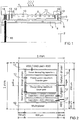
- Figure 2 shows a layout of a backside illuminated image sensor comprising capacitors above the detector elements.
- the position of the cross-section shown in Figure 1 is indicated in Figure 2 .
- the capacitors which may include power decoupling capacitors, charge pump capacitors for the transfer gates and the reset gates of the pixels, capacitors for the stabilization of the clock generation and capacitors for analog-to-digital conversion references, for example, are arranged in the centre.
- the arrangement of the capacitors may occupy a central area of typically 800 ⁇ m ⁇ 800 ⁇ m, which may be surrounded by a peripheral area having typically a width of 100 ⁇ m or less.
- Some typical components of the peripheral circuit 12 are named in the layout shown in Figure 2 .
- Figure 3 is a top view of a suitable layout of a backside illuminated image sensor, which shows an example of the arrangement of the pixels and the capacitor layers.
- the first capacitor layer 7 forms a plurality of strips, which are the bottom capacitor plates.
- the second capacitor layer 8 forms a further plurality of strips, which are the top capacitor plates.
- the strips of the first capacitor layer 7 are arranged parallel at a distance from one another and are aligned with the strips of the second capacitor layer 8 and with rows of detector elements 11. Thus a plurality of capacitors is formed.
- connection of the capacitors to the peripheral circuit 12 may especially allow to use a common capacitor plate.
- one of the first and second capacitor layers 7, 8 may be an entire layer or may be divided into sections that are larger than the strips shown in Figure 3 .
- Figure 4 is a further top view of a suitable layout and shows a further example of the arrangement of the pixels and the capacitor layers.
- the first capacitor layer 7 forms a plurality of parallel spaced apart strips, which are the bottom capacitor plates
- the second capacitor layer 8 forms a plurality of parallel spaced apart strips, which are the top capacitor plates.
- the strips of the second capacitor layer 8 are arranged transverse to the strips of the first capacitor layer 7.
- the strips of the first capacitor layer 7 and the strips of the second capacitor layer 8 are aligned with rows of the detector elements 11 along two directions at a right angle.
- the shape of the capacitor layers according to Figures 3 and 4 provides similar optical behaviour in all pixels. Additionally, the pattern of the capacitor layers 7, 8 may be designed for a backside reflection including a scattering effect in order to have the incident radiation completely absorbed. This may be desired in large photodiode structures, which are used in light sensors, for example.
- Figure 5 is a cross-section according to Figure 1 for an image sensor comprising a capacitor formed by an interdigitated structure. Elements of the image sensor according to Figure 5 that correspond to elements of the image sensor according to Figure 1 are designated with the same reference numerals.
- the first and second capacitor layers 7, 8 are structured in parallel strips, which are arranged at small distances from one another. According to their spatial succession, these strips are alternatingly electrically connected to one another and to the same contact region 13 of the peripheral circuit 12.
- the electrically connected sections of the first capacitor layer 7 and the electrically connected sections of the second capacitor layer 8 are respectively indicated in Figure 5 by the same type of hatching.
- the sections of the first capacitor layer 7, which are connected to the contact region 13 marked "a”, are shown with a double hatching, whereas the sections of the second capacitor layer 8, which are connected to the contact region 13 marked "b", are shown with a single hatching.
- an optional further electrically conductive layer 6 forms a common capacitor plate, which is connected to the contact region 13 marked "com".
- the further electrically conductive layer 6 may instead be structured into separate sections forming further capacitor plates.
- An interdigitated structure of capacitor plates is formed within the same layer by the strips of the first and second capacitor layers 7, 8 according to Figure 5 .
- the capacitor dielectric is provided by the regions of the dielectric layer 3 that are present between the strips.
- such an interdigitated structure of capacitor plates may be formed in a further layer.
- the further electrically conductive layer 6 covers the entire area that is occupied by the detector elements 11.
- the further electrically conductive layer 6 is thus also suitable as an electrical shield or a light reflector enabling a uniform reflection of the incident radiation to the focal plane.
- the further electrically conductive layer 6 may be a light absorbing layer, which prevents radiation from being reflected back into the semiconductor material.
- An absorbing layer may be advantageous to avoid fringing effects, which generate undesired patterns in an image. Fringing effects can be due to tiny thickness variations of a thin silicon substrate.
- a metal may be suitable for an absorbing layer.
- Figure 6 is a circuit diagram showing the connection of the capacitors of the image sensor according to Figure 5 .
- the sections of the first capacitor layer 7 and the sections of the second capacitor layer 8 form a further capacitor C.
- Each capacitor plate of the further capacitor C is also a plate of either the first capacitor C1 or the second capacitor C2.
- Figure 7 is a cross-section according to Figure 1 for an image sensor with electrically conductive layers provided on both substrates. Elements of the image sensor according to Figure 7 that correspond to elements of the image sensor according to Figure 1 are designated with the same reference numerals.
- a further dielectric layer 19 is provided on the further substrate 2.
- the bonding layer 4, which may be silicon dioxide, for instance, is arranged between the dielectric layer 3 and the further dielectric layer 19.
- the bonding layer 4 is optional; the dielectric layer 3 may be bonded directly to the further dielectric layer 19.
- the first capacitor layer 7 and the second capacitor layer 8 are embedded in the further dielectric layer 19.
- the electric connections 9 between the contact regions 13 and the capacitor layers 7, 8 penetrate the bonding layer 4 and reach into the further dielectric layer 19.
- a capacitor connection 17 may be provided for an electric connection of the first capacitor layer 7 with the structured electrically conductive layer 5 or with a further structured electrically conductive layer 6 in the dielectric layer 3
- a further capacitor connection 18 may be provided for an electric connection of the second capacitor layer 8 with the structured electrically conductive layer 5 or with a further structured electrically conductive layer 6 in the dielectric layer 3.
- the first capacitor layer 7 covers the entire area that is occupied by the detector elements 11. Therefore the first capacitor layer 7 is also suitable as a light reflector or an electrical shield.
- Figure 7 also shows an optional reflecting layer 20, which may be arranged on or in the further dielectric layer 19. The reflecting layer 20 is thus located between the dielectric layer 3 and the capacitor layers 7, 8. The reflecting layer 20 may in particular be arranged between the bonding layer 4 and the further dielectric layer 19.
- Figure 8 is a cross-section according to Figure 1 for an image sensor with stacked capacitors. Elements of the image sensor according to Figure 8 that correspond to elements of the image sensor according to Figure 1 are designated with the same reference numerals.
- a third capacitor layer 21 and a fourth capacitor layer 22 are provided in the image sensor according to Figure 8 .
- the capacitor layers 7, 8, 21, 22 are arranged in a vertical sequence and separated from one another by portions of the dielectric layer 3. Thus a first capacitor C1 and a second capacitor C2 are arranged one above the other.
- first capacitor layer 7 and the third capacitor layer 21 are electrically connected, and the second capacitor layer 8 and the fourth capacitor layer 22 are also electrically connected.
- first capacitor C1 and the second capacitor C2 are connected in parallel, so that the capacitances of the first capacitor C1 and the second capacitor C2 are added.
- Other electric connections may instead be suitable for further embodiments of the image sensor.
- Figure 9 is a cross-section according to Figure 8 for a further example of an image sensor with stacked capacitors. Elements of the image sensor according to Figure 9 that correspond to elements of the image sensor according to Figure 8 are designated with the same reference numerals.
- the first capacitor layer 7 and the third capacitor layer 21 are connected with different contact regions 13, while the second capacitor layer 8 and the fourth capacitor layer 22 are electrically connected.
- Figure 10 is a cross-section according to Figure 1 for an image sensor with a capacitor comprising a three-dimensional structure. Elements of the image sensor according to Figure 10 that correspond to elements of the image sensor according to Figure 1 are designated with the same reference numerals.
- the first capacitor layer 7 and the second capacitor layer 8 are arranged in trenches 23 formed in the dielectric layer 3. The capacitance of the capacitor can be substantially increased by such a three-dimensional structure.
- the first capacitor layer 7 can form a further capacitor with the optional further electrically conductive layer 6, for example.
- the further electrically conductive layer 6 may also serve as a light shield or as an absorbing layer.
- the capacitors can be placed at the front side of the pixel array without increasing the size of the image sensor. This is advantageous for applications in miniature camera modules, for instance.
- Such variation may be caused by changes in current consumption of the image sensor or the tip of the endoscopy camera. Variations in current consumption may occur, for example, when the sensor switches from exposure to readout. This can cause a change in the signals read at the first rows of the image. Current consumption may also be dependent on the signal levels. E. g. a sensor may consume more current when reading white pixels than black pixels. In that case the content of the image can determine current consumption. If the supply varies with this consumption, certain patterns may occur in the image sensor (like horizontal bands at left and right of a white area or vertical tails under white exposed areas).
- a stabler clock improves readout characteristics, as exposure times, frame rate and data rates are stabler.
- the signal is easier to recover at the receiver side. It is also easier to synchronize multiple devices, e. g. a stereo camera pair, or a light source and an image sensor.
- On-chip voltage regulators make it possible to improve the performance of the pixels.
- a high voltage for the pixel reset level can be generated on chip by charge pumps to increase the dynamic range.
- Negative voltages can be created on-chip to drive the transfer gate and improve the dark current and dynamic range.
- a uniform bottom plate ensures similar electrical coupling to the high impedance nodes of the pixel circuit, such as the floating diffusion (sense node). That is important to avoid any differences in gain of the pixels or any signal-dependent interferences.
- a uniform large bottom plate may be connected to ground, V DD or another fixed reference voltage.
- the capacitor can also be constructed by an identical pattern in each pixel. This allows to comply with maximum density coverage rules and to use capacitors with two floating terminals. This scheme can be extended to a repetitive pattern per pairs of pixels or four or more pixels.
- the described backside illuminated image sensor allows an integration of capacitors outside the region surrounding the pixel array of the image sensor.
- This integration scheme enables to realize a very compact image sensor and at the same time to achieve a substantial improvement of its performance.
Landscapes
- Solid State Image Pick-Up Elements (AREA)
- Transforming Light Signals Into Electric Signals (AREA)
Abstract
Description
- Backside illuminated image sensors comprise a plurality of detector elements forming a pixel array for image detection. The pixel array is surrounded by a peripheral area, in which readout circuits are disposed, in particular CMOS circuits, including row logic, column amplifiers, analog-to-digital converters, clock generation and output drivers. The width of the peripheral area may be less than 100 µm. Very small dimensions of the image sensor are required in many applications, for which endoscopes are a typical example.
- The image quality is improved if a capacitive decoupling is provided for the readout circuitry of the image sensor. It may be favourable if the driving voltage of the transfer gate of a pixel is negative in order to reduce the dark current and improve the dynamic range, as discussed by H. Han et al., "Evaluation of a Small Negative Transfer Gate Bias on the Performance of 4T CMOS Image Sensor Pixels", International Image Sensor Workshop 2007, pp 238-240. It may also be favourable if the driving voltage of the reset gate of a pixel is higher than the supply voltage.
- Variations in the current consumption of the sensor can cause ripple on the supply voltage, which may also be prone to interference. The frequency of an oscillator, which is integrated for the generation of clock signals that control the operation of the sensor, may depend on the supply voltage and the ambient temperature. A control circuitry is therefore usually required to be integrated in the image sensor.
-
WO 2013/091123 A1 discloses an optical sensor arrangement, in particular for use in an endoscope, which has a multi-wire line as an electrical connection between the distal end and the proximal end. The optical sensor arrangement is mounted directly on the multi-wire line. -
US 2014/0030842 A1 discloses a backside illuminated image sensor comprising a semiconductor substrate, a sensor element at the front side of the substrate, and a capacitor overlying the sensor element. The capacitor increases a floating capacitance created between transistor connections and can also meet other circuit design needs, such as A/D conversion. -
US 2014/0300698 A1 discloses an endoscopic arrangement provided with a plurality of image sensors, each of which generates a sensor clock by an uncontrolled oscillator. An electronic control circuitry detects the sensor clock and/or the sensor frame rate and/or the sensor image phase and adjusts the detected information to a reference clock. - G. Meynants et al., "Backside illuminated CMOS active pixel sensor with global shutter and 84 dB dynamic range", Scientific Detector Workshop, Florence 2013, describe the use of MiM capacitors for the sampling of pixel signals. The capacitors are disposed at the front side of a CIS global shutter pixel.
- Y. Kagawa et al., "Novel Stacked CMOS Image Sensor with Advanced Cu2Cu Hybrid Bonding", Proc. IEDM, 2016, pp. 8.4.1-8.4.4, describe 3D stacked CMOS image sensors including a backside illuminated CMOS image sensor that is wafer-bonded to a CMOS readout IC.
- It is an object of the present invention to present a compact backside illuminated image sensor including capacitors provided for voltage regulation, charge pump operation or stabilization of on-chip clock generation.
- This object is achieved with the backside illuminated image sensor according to
claim 1. Embodiments derive from the dependent claims. - The backside illuminated image sensor comprises a substrate of semiconductor material having a main surface, detector elements arranged at the main surface, a dielectric layer on or above the main surface, a first capacitor layer of electrically conductive material embedded in the dielectric layer and a second capacitor layer of electrically conductive material embedded in the dielectric layer at a distance from the first capacitor layer. The first and second capacitor layers form at least one capacitor.
- A peripheral circuit is integrated in the substrate apart from the detector elements. The peripheral circuit is configured for voltage regulation and/or charge pump operation and/or stabilization of clock generation. The first and second capacitor layers are electrically connected with contact regions of the peripheral circuit.
- The electrically conductive material may be a metal or electrically conductive polysilicon, for instance. Tungsten is a suitable metal, for instance. The capacitor layers may especially be formed by metallizations of a wiring. They may include additional electrically conductive layers arranged between the metallization levels of the wiring.
- The capacitor may be formed on one level, in particular by interdigitated capacitor layers, or as a three-dimensional structure, in particular as a trench capacitor for large capacitance. A large capacitance per unit area can also be achieved by making the distance between the capacitor layers small and arranging HfO, Al2O3 or another high-κ dielectric in between.
- One or more structured electrically conductive layers can be embedded in the dielectric layer, additionally to the capacitor layers. Electric connections can be provided to connect the capacitor layers to parts of the structured electrically conductive layer(s).
- In an embodiment of the backside illuminated image sensor, at least one of the first and second capacitor layers comprises parallel strips arranged at a distance from one another. Each of the first and second capacitor layers may comprise parallel strips arranged at a distance from one another. In particular, the strips of the first capacitor layer may be parallel to the strips of the second capacitor layer, or the strips of the first capacitor layer may be transverse to the strips of the second capacitor layer.
- In a further embodiment of the backside illuminated image sensor, the strips of the first capacitor layer and the strips of the second capacitor layer are interdigitated, the strips of the first capacitor layer are electrically connected to one another, and the strips of the second capacitor layer are electrically connected to one another.
- In a further embodiment, the first and second capacitor layers are arranged in a three-dimensional structure.
- In a further embodiment, the peripheral circuit has a width of less than 100 µm.
- In a further embodiment, the peripheral circuit surrounds the detector elements.
- A further embodiment comprises a further substrate of semiconductor material, which is bonded to the substrate. The dielectric layer is arranged between the substrate and the further substrate.
- A further embodiment comprises a further dielectric layer on the further substrate. The further dielectric layer is arranged between the further substrate and the dielectric layer. The first capacitor layer and the second capacitor layer may be embedded in the further dielectric layer.
- A further embodiment comprises a through-substrate interconnection penetrating the further substrate.
- A further embodiment comprises a further contact region in the peripheral circuit and a further electric connection connecting the through-substrate interconnection with the further contact region.
- The following is a detailed description of examples of the backside illuminated image sensor in conjunction with the appended figures.
- Figure 1
- is a cross-section of a backside illuminated image sensor with capacitors above the detector elements.
- Figure 2
- shows a layout of a backside illuminated image sensor with capacitors above the detector elements.
- Figure 3
- is a top view of an arrangement of the pixels and the capacitor layers.
- Figure 4
- is a top view of a further arrangement of the pixels and the capacitor layers.
- Figure 5
- is a cross-section according to
Figure 1 for a backside illuminated image sensor comprising a capacitor formed by an interdigitated structure. - Figure 6
- is a circuit diagram showing the connection of the capacitors of the device according to
Figure 5 . - Figure 7
- is a cross-section according to
Figure 1 for a backside illuminated image sensor with electrically conductive layers arranged in dielectric layers of two substrates. - Figure 8
- is a cross-section according to
Figure 1 for a backside illuminated image sensor with stacked capacitors. - Figure 9
- is a cross-section according to
Figure 8 for a further backside illuminated image sensor with stacked capacitors. - Figure 10
- is a cross-section according to
Figure 1 for a backside illuminated image sensor with trench capacitors. -
Figure 1 is a cross-section of a backside illuminated image sensor. It comprises asubstrate 1 of semiconductor material, which may be silicon, for instance. Adielectric layer 3, which may be silicon dioxide, for instance, is arranged on or above amain surface 10 of thesubstrate 1. A structured electricallyconductive layer 5 is optionally embedded in thedielectric layer 3. The structured electricallyconductive layer 5 may be provided as a pixel routing layer, for instance. It may be part of a wiring, which may comprise further structured electrically conductive layers and vertical interconnections. In particular, the structured electricallyconductive layer 5 may be provided for horizontal connections, like control lines for charge transfer, for instance, and a further structured electrically conductive layer may be provided for vertical connections used for output and power supply, for instance. -
Detector elements 11, which may be photodiodes, for instance, are arranged in thesubstrate 1 at themain surface 10. Thedetector elements 11 can especially be arranged in an array for image detection. Eachdetector element 11 can thus be employed to yield a pixel of an image that is to be detected. - A
peripheral circuit 12 is integrated in thesubstrate 1 apart from thedetector elements 11. The region occupied by theperipheral circuit 12 is outside the region where thedetector elements 11 are disposed. Theperipheral circuit 12 may especially surround the region of thedetector elements 11.Peripheral circuit 12 could also be at one side only. - A
first capacitor layer 7 of electrically conductive material and asecond capacitor layer 8 of electrically conductive material are arranged at a distance from one another in thedielectric layer 3 and form a capacitor C1. The number of capacitors thus formed is arbitrary.Figure 1 shows one further capacitor C2 by way of example. - The electrically conductive material of the first and second capacitor layers 7, 8 may be a metal, in particular tungsten, aluminum or copper, for instance, or electrically conductive polysilicon, for instance. The capacitor dielectric may be a portion of the
dielectric layer 3. Instead, a different capacitor dielectric may be arranged between the first and second capacitor layers 7, 8. A metal-insulator-metal capacitor of increased capacitance may be obtained by arranging a dedicated capacitor dielectric of high relative permittivity between the first and second capacitor layers 7, 8. - The sections of the
first capacitor layer 7 and thesecond capacitor layer 8 are each electrically connected to contactregions 13 of theperipheral circuit 12 by verticalelectric connections 9 in thedielectric layer 3. Thus the capacitors C1, C2 are connected to theperipheral circuit 12 and form components of the integrated circuit. -
Figure 1 shows an example of thefirst capacitor layer 7 that covers the entire area of thedetector elements 11. Thefirst capacitor layer 7 is thus also suitable as an electrical shield or a light reflector enabling a uniform reflection of the incident radiation to the focal plane. - In the example of the image sensor shown in
Figure 1 , an optionalfurther substrate 2 is bonded to thedielectric layer 3. Thefurther substrate 2 may be a further semiconductor substrate, in particular a handling wafer, for instance. It may comprise electric components, in particular passive components like conductor tracks and resistors. Thefurther substrate 2 may be bonded directly to thedielectric layer 3, or abonding layer 4, which may be silicon dioxide, for instance, may be provided for this purpose. - The
further substrate 2 may comprise an electrically conductive through-substrate interconnection 16, which is formed by an electrically conductive material arranged in a via penetrating thefurther substrate 2. Afurther contact region 14 of theperipheral circuit 12 and a furtherelectric connection 15 in thedielectric layer 3 may be provided for an electric connection of theperipheral circuit 12 to the through-substrate interconnection 16. -
Figure 2 shows a layout of a backside illuminated image sensor comprising capacitors above the detector elements. The position of the cross-section shown inFigure 1 is indicated inFigure 2 . The capacitors, which may include power decoupling capacitors, charge pump capacitors for the transfer gates and the reset gates of the pixels, capacitors for the stabilization of the clock generation and capacitors for analog-to-digital conversion references, for example, are arranged in the centre. The arrangement of the capacitors may occupy a central area of typically 800 µm × 800 µm, which may be surrounded by a peripheral area having typically a width of 100 µm or less. Some typical components of theperipheral circuit 12 are named in the layout shown inFigure 2 . -
Figure 3 is a top view of a suitable layout of a backside illuminated image sensor, which shows an example of the arrangement of the pixels and the capacitor layers. Thefirst capacitor layer 7 forms a plurality of strips, which are the bottom capacitor plates. Thesecond capacitor layer 8 forms a further plurality of strips, which are the top capacitor plates. The strips of thefirst capacitor layer 7 are arranged parallel at a distance from one another and are aligned with the strips of thesecond capacitor layer 8 and with rows ofdetector elements 11. Thus a plurality of capacitors is formed. - The connection of the capacitors to the
peripheral circuit 12 may especially allow to use a common capacitor plate. In this case one of the first and second capacitor layers 7, 8 may be an entire layer or may be divided into sections that are larger than the strips shown inFigure 3 . -
Figure 4 is a further top view of a suitable layout and shows a further example of the arrangement of the pixels and the capacitor layers. In the example according toFigure 4 , thefirst capacitor layer 7 forms a plurality of parallel spaced apart strips, which are the bottom capacitor plates, and thesecond capacitor layer 8 forms a plurality of parallel spaced apart strips, which are the top capacitor plates. The strips of thesecond capacitor layer 8 are arranged transverse to the strips of thefirst capacitor layer 7. The strips of thefirst capacitor layer 7 and the strips of thesecond capacitor layer 8 are aligned with rows of thedetector elements 11 along two directions at a right angle. - The shape of the capacitor layers according to
Figures 3 and 4 provides similar optical behaviour in all pixels. Additionally, the pattern of the capacitor layers 7, 8 may be designed for a backside reflection including a scattering effect in order to have the incident radiation completely absorbed. This may be desired in large photodiode structures, which are used in light sensors, for example. -
Figure 5 is a cross-section according toFigure 1 for an image sensor comprising a capacitor formed by an interdigitated structure. Elements of the image sensor according toFigure 5 that correspond to elements of the image sensor according toFigure 1 are designated with the same reference numerals. In the image sensor according toFigure 5 , the first and second capacitor layers 7, 8 are structured in parallel strips, which are arranged at small distances from one another. According to their spatial succession, these strips are alternatingly electrically connected to one another and to thesame contact region 13 of theperipheral circuit 12. - The electrically connected sections of the
first capacitor layer 7 and the electrically connected sections of thesecond capacitor layer 8 are respectively indicated inFigure 5 by the same type of hatching. The sections of thefirst capacitor layer 7, which are connected to thecontact region 13 marked "a", are shown with a double hatching, whereas the sections of thesecond capacitor layer 8, which are connected to thecontact region 13 marked "b", are shown with a single hatching. - In the example shown in
Figure 5 , an optional further electricallyconductive layer 6 forms a common capacitor plate, which is connected to thecontact region 13 marked "com". The further electricallyconductive layer 6 may instead be structured into separate sections forming further capacitor plates. - An interdigitated structure of capacitor plates is formed within the same layer by the strips of the first and second capacitor layers 7, 8 according to
Figure 5 . The capacitor dielectric is provided by the regions of thedielectric layer 3 that are present between the strips. Instead or additionally, such an interdigitated structure of capacitor plates may be formed in a further layer. - In the image sensor according to
Figure 5 , the further electricallyconductive layer 6 covers the entire area that is occupied by thedetector elements 11. The further electricallyconductive layer 6 is thus also suitable as an electrical shield or a light reflector enabling a uniform reflection of the incident radiation to the focal plane. - Alternatively, the further electrically
conductive layer 6 may be a light absorbing layer, which prevents radiation from being reflected back into the semiconductor material. An absorbing layer may be advantageous to avoid fringing effects, which generate undesired patterns in an image. Fringing effects can be due to tiny thickness variations of a thin silicon substrate. A metal may be suitable for an absorbing layer. -
Figure 6 is a circuit diagram showing the connection of the capacitors of the image sensor according toFigure 5 . The common capacitor plate that is provided by the further electricallyconductive layer 6 and the sections of thefirst capacitor layer 7, which are connected to thecontact region 13 marked "a", form a first capacitor C1. The common capacitor plate that is provided by the further electricallyconductive layer 6 and the sections of thesecond capacitor layer 8, which are connected to thecontact region 13 marked "b", form a second capacitor C2. The sections of thefirst capacitor layer 7 and the sections of thesecond capacitor layer 8 form a further capacitor C. Each capacitor plate of the further capacitor C is also a plate of either the first capacitor C1 or the second capacitor C2. -
Figure 7 is a cross-section according toFigure 1 for an image sensor with electrically conductive layers provided on both substrates. Elements of the image sensor according toFigure 7 that correspond to elements of the image sensor according toFigure 1 are designated with the same reference numerals. In the image sensor according toFigure 7 , afurther dielectric layer 19 is provided on thefurther substrate 2. Thebonding layer 4, which may be silicon dioxide, for instance, is arranged between thedielectric layer 3 and thefurther dielectric layer 19. Thebonding layer 4 is optional; thedielectric layer 3 may be bonded directly to thefurther dielectric layer 19. - In the image sensor according to
Figure 7 , thefirst capacitor layer 7 and thesecond capacitor layer 8 are embedded in thefurther dielectric layer 19. Theelectric connections 9 between thecontact regions 13 and the capacitor layers 7, 8 penetrate thebonding layer 4 and reach into thefurther dielectric layer 19. Furthermore, acapacitor connection 17 may be provided for an electric connection of thefirst capacitor layer 7 with the structured electricallyconductive layer 5 or with a further structured electricallyconductive layer 6 in thedielectric layer 3, and afurther capacitor connection 18 may be provided for an electric connection of thesecond capacitor layer 8 with the structured electricallyconductive layer 5 or with a further structured electricallyconductive layer 6 in thedielectric layer 3. - In the image sensor according to
Figure 7 , thefirst capacitor layer 7 covers the entire area that is occupied by thedetector elements 11. Therefore thefirst capacitor layer 7 is also suitable as a light reflector or an electrical shield.Figure 7 also shows an optional reflecting layer 20, which may be arranged on or in thefurther dielectric layer 19. The reflecting layer 20 is thus located between thedielectric layer 3 and the capacitor layers 7, 8. The reflecting layer 20 may in particular be arranged between thebonding layer 4 and thefurther dielectric layer 19. -
Figure 8 is a cross-section according toFigure 1 for an image sensor with stacked capacitors. Elements of the image sensor according toFigure 8 that correspond to elements of the image sensor according toFigure 1 are designated with the same reference numerals. In the image sensor according toFigure 8 , athird capacitor layer 21 and afourth capacitor layer 22 are provided. The capacitor layers 7, 8, 21, 22 are arranged in a vertical sequence and separated from one another by portions of thedielectric layer 3. Thus a first capacitor C1 and a second capacitor C2 are arranged one above the other. - In the example shown in
Figure 8 , thefirst capacitor layer 7 and thethird capacitor layer 21 are electrically connected, and thesecond capacitor layer 8 and thefourth capacitor layer 22 are also electrically connected. Thus the first capacitor C1 and the second capacitor C2 are connected in parallel, so that the capacitances of the first capacitor C1 and the second capacitor C2 are added. Other electric connections may instead be suitable for further embodiments of the image sensor. -
Figure 9 is a cross-section according toFigure 8 for a further example of an image sensor with stacked capacitors. Elements of the image sensor according toFigure 9 that correspond to elements of the image sensor according toFigure 8 are designated with the same reference numerals. In the image sensor according toFigure 9 , thefirst capacitor layer 7 and thethird capacitor layer 21 are connected withdifferent contact regions 13, while thesecond capacitor layer 8 and thefourth capacitor layer 22 are electrically connected. -
Figure 10 is a cross-section according toFigure 1 for an image sensor with a capacitor comprising a three-dimensional structure. Elements of the image sensor according toFigure 10 that correspond to elements of the image sensor according toFigure 1 are designated with the same reference numerals. In the image sensor according toFigure 10 , thefirst capacitor layer 7 and thesecond capacitor layer 8 are arranged intrenches 23 formed in thedielectric layer 3. The capacitance of the capacitor can be substantially increased by such a three-dimensional structure. Furthermore, thefirst capacitor layer 7 can form a further capacitor with the optional further electricallyconductive layer 6, for example. The further electricallyconductive layer 6 may also serve as a light shield or as an absorbing layer. - By combining the capacitor structures shown in
Figures 1 ,5 ,7, 8 ,9 and 10 , a variety of circuits can be realized in a very compact semiconductor device. - As the image sensor is illuminated from the rear side, the capacitors can be placed at the front side of the pixel array without increasing the size of the image sensor. This is advantageous for applications in miniature camera modules, for instance.
- Better decoupling of the power supply makes the image sensor less sensitive to variation in the supplied voltage. Such variation may be caused by changes in current consumption of the image sensor or the tip of the endoscopy camera. Variations in current consumption may occur, for example, when the sensor switches from exposure to readout. This can cause a change in the signals read at the first rows of the image. Current consumption may also be dependent on the signal levels. E. g. a sensor may consume more current when reading white pixels than black pixels. In that case the content of the image can determine current consumption. If the supply varies with this consumption, certain patterns may occur in the image sensor (like horizontal bands at left and right of a white area or vertical tails under white exposed areas).
- A stabler clock improves readout characteristics, as exposure times, frame rate and data rates are stabler. The signal is easier to recover at the receiver side. It is also easier to synchronize multiple devices, e. g. a stereo camera pair, or a light source and an image sensor.
- On-chip voltage regulators make it possible to improve the performance of the pixels. A high voltage for the pixel reset level can be generated on chip by charge pumps to increase the dynamic range. Negative voltages can be created on-chip to drive the transfer gate and improve the dark current and dynamic range.
- A uniform bottom plate ensures similar electrical coupling to the high impedance nodes of the pixel circuit, such as the floating diffusion (sense node). That is important to avoid any differences in gain of the pixels or any signal-dependent interferences. A uniform large bottom plate may be connected to ground, VDD or another fixed reference voltage. In order to keep the back reflectance and capacitive coupling identical in all pixels, the capacitor can also be constructed by an identical pattern in each pixel. This allows to comply with maximum density coverage rules and to use capacitors with two floating terminals. This scheme can be extended to a repetitive pattern per pairs of pixels or four or more pixels.
- The described backside illuminated image sensor allows an integration of capacitors outside the region surrounding the pixel array of the image sensor. This integration scheme enables to realize a very compact image sensor and at the same time to achieve a substantial improvement of its performance.
-
- 1
- substrate
- 2
- further substrate
- 3
- dielectric layer
- 4
- bonding layer
- 5
- electrically conductive layer
- 6
- further electrically conductive layer
- 7
- first capacitor layer
- 8
- second capacitor layer
- 9
- electric connection
- 10
- main surface
- 11
- detector element
- 12
- peripheral circuit
- 13
- contact region
- 14
- further contact region
- 15
- further electric connection
- 16
- through-substrate interconnection
- 17
- capacitor connection
- 18
- further capacitor connection
- 19
- further dielectric layer
- 20
- reflecting layer
- 21
- third capacitor layer
- 22
- fourth capacitor layer
- 23
- trench
- C
- further capacitor
- C1
- first capacitor
- C2
- second capacitor
Claims (16)
- A backside illuminated image sensor, comprising:- a substrate (1) of semiconductor material having a main surface (10),- detector elements (11) arranged at the main surface (10),- a dielectric layer (3, 19) on or above the main surface (10),- a first capacitor layer (7) of electrically conductive material embedded in the dielectric layer (3, 19), and- a second capacitor layer (8) of electrically conductive material embedded in the dielectric layer (3, 19) at a distance from the first capacitor layer (7), the first and second capacitor layers (7, 8) forming a capacitor (C1, C2),characterized in that- a peripheral circuit (12) is integrated in the substrate (1) apart from the detector elements (11), the peripheral circuit (12) being configured for one or more operations of the group consisting of voltage regulation, charge pump operation and stabilization of clock generation, and- the first and second capacitor layers (7, 8) are electrically connected with contact regions (13) of the peripheral circuit (12).
- The backside illuminated image sensor of claim 1, wherein at least one of the first and second capacitor layers (7, 8) comprises parallel strips arranged at a distance from one another.
- The backside illuminated image sensor of claim 1, wherein each of the first and second capacitor layers (7, 8) comprises parallel strips arranged at a distance from one another.
- The backside illuminated image sensor of claim 3, wherein the strips of the first capacitor layer (7) are parallel to the strips of the second capacitor layer (8).
- The backside illuminated image sensor of claim 4, wherein the strips of the first capacitor layer (7) and the strips of the second capacitor layer (8) are interdigitated, the strips of the first capacitor layer (7) are electrically connected to one another, and the strips of the second capacitor layer (8) are electrically connected to one another.
- The backside illuminated image sensor of claim 3, wherein the strips of the first capacitor layer (7) are transverse to the strips of the second capacitor layer (8).
- The backside illuminated image sensor of claim 1, wherein the first and second capacitor layers (7, 8) are arranged in a three-dimensional structure.
- The backside illuminated image sensor of one of claims 1 to 7, wherein the first capacitor layer (7) and/or the second capacitor layer (8) comprises metal.
- The backside illuminated image sensor of one of claims 1 to 7, wherein the first capacitor layer (7) and/or the second capacitor layer (8) comprises polysilicon.
- The backside illuminated image sensor of one of claims 1 to 9, wherein a high-κ dielectric is arranged between the first capacitor layer (7) and the second capacitor layer (8).
- The backside illuminated image sensor of one of claims 1 to 10, wherein the peripheral circuit (12) has a width of less than 100 µm.
- The backside illuminated image sensor of one of claims 1 to 11, wherein the peripheral circuit (12) surrounds the detector elements (11).
- The backside illuminated image sensor of one of claims 1 to 12, further comprising:a further substrate (2) of semiconductor material, thefurther substrate (2) being bonded to the substrate (1), andthe dielectric layer (3) being arranged between the substrate (1) and the further substrate (2).
- The backside illuminated image sensor of claim 13, further comprising:a further dielectric layer (19) on the further substrate (2),the further dielectric layer (19) being arranged between the further substrate (2) and the dielectric layer (3), andthe first capacitor layer (7) and the second capacitor layer (8) being embedded in the further dielectric layer (19).
- The backside illuminated image sensor of claim 13 or 14, further comprising:a through-substrate interconnection (16) penetrating the further substrate (2).
- The backside illuminated image sensor of claim 15, further comprising:- a further contact region (14) in the peripheral circuit (12), and- a further electric connection (15) connecting the through-substrate interconnection (16) with the further contact region (14).
Priority Applications (5)
| Application Number | Priority Date | Filing Date | Title |
|---|---|---|---|
| EP17173499.9A EP3410485B1 (en) | 2017-05-30 | 2017-05-30 | Backside illuminated image sensor |
| TW107114507A TWI670839B (en) | 2017-05-30 | 2018-04-27 | Backside illuminated image sensor |
| CN201880033123.1A CN110637371B (en) | 2017-05-30 | 2018-05-07 | back-illuminated image sensor |
| US16/616,581 US11322532B2 (en) | 2017-05-30 | 2018-05-07 | Backside illuminated image sensor |
| PCT/EP2018/061711 WO2018219592A1 (en) | 2017-05-30 | 2018-05-07 | Backside illuminated image sensor |
Applications Claiming Priority (1)
| Application Number | Priority Date | Filing Date | Title |
|---|---|---|---|
| EP17173499.9A EP3410485B1 (en) | 2017-05-30 | 2017-05-30 | Backside illuminated image sensor |
Publications (2)
| Publication Number | Publication Date |
|---|---|
| EP3410485A1 true EP3410485A1 (en) | 2018-12-05 |
| EP3410485B1 EP3410485B1 (en) | 2022-08-03 |
Family
ID=59070410
Family Applications (1)
| Application Number | Title | Priority Date | Filing Date |
|---|---|---|---|
| EP17173499.9A Active EP3410485B1 (en) | 2017-05-30 | 2017-05-30 | Backside illuminated image sensor |
Country Status (5)
| Country | Link |
|---|---|
| US (1) | US11322532B2 (en) |
| EP (1) | EP3410485B1 (en) |
| CN (1) | CN110637371B (en) |
| TW (1) | TWI670839B (en) |
| WO (1) | WO2018219592A1 (en) |
Cited By (1)
| Publication number | Priority date | Publication date | Assignee | Title |
|---|---|---|---|---|
| US11930288B2 (en) | 2018-11-30 | 2024-03-12 | Ams Sensors Belgium Bvba | Pixel drive voltage generation using a charge pump |
Families Citing this family (12)
| Publication number | Priority date | Publication date | Assignee | Title |
|---|---|---|---|---|
| US8906320B1 (en) | 2012-04-16 | 2014-12-09 | Illumina, Inc. | Biosensors for biological or chemical analysis and systems and methods for same |
| PH12019502895B1 (en) * | 2017-12-26 | 2024-04-24 | Illumina Inc | Sensor system |
| US11335768B2 (en) * | 2018-04-16 | 2022-05-17 | Semtech Corporation | Integrated high voltage capacitor |
| KR102624610B1 (en) * | 2018-10-04 | 2024-01-15 | 삼성전자주식회사 | Image sensor |
| KR102618358B1 (en) * | 2019-06-05 | 2023-12-28 | 삼성전자주식회사 | Image sensor |
| CN112054032B (en) * | 2019-06-05 | 2025-10-31 | 三星电子株式会社 | Image sensor |
| US11227847B2 (en) * | 2020-03-04 | 2022-01-18 | Cisco Technology, Inc. | Integrated decoupling capacitors |
| US11437323B2 (en) * | 2020-06-03 | 2022-09-06 | Hewlett Packard Enterprise Development Lp | Silicon interposer for capacitive coupling of photodiode arrays |
| US12094891B2 (en) * | 2020-07-13 | 2024-09-17 | Drs Network & Imaging Systems, Llc | High-density capacitor for focal plane arrays |
| KR102812763B1 (en) | 2020-08-13 | 2025-05-23 | 삼성전자주식회사 | Image sensor |
| JP2023172505A (en) * | 2022-05-24 | 2023-12-06 | キヤノン株式会社 | Photoelectric conversion device |
| US20240355865A1 (en) * | 2023-04-21 | 2024-10-24 | Taiwan Semiconductor Manufacturing Company, Ltd. | Semiconductor capacitor for image sensor pixel circuitry |
Citations (8)
| Publication number | Priority date | Publication date | Assignee | Title |
|---|---|---|---|---|
| WO1996027907A1 (en) * | 1995-03-03 | 1996-09-12 | Northern Telecom Limited | Capacitor structure for an integrated circuit and method of fabrication thereof |
| US20080305572A1 (en) * | 2007-06-05 | 2008-12-11 | Samsung Electronics Co., Ltd. | Method of fabricating image device having capacitor and image device fabricated thereby |
| US20110049589A1 (en) * | 2009-09-01 | 2011-03-03 | Taiwan Semiconductor Manufacturing Company, Ltd. | Backside illuminated image sensor having capacitor on pixel region |
| US20110278687A1 (en) * | 2010-05-17 | 2011-11-17 | Fang-Ming Huang | Backside-illuminated sensor with noise reduction |
| US20120187514A1 (en) * | 2011-01-21 | 2012-07-26 | Aptina Imaging Corporation | System for reducing sensor area in a back side illuminated cmos active pixel sensor |
| WO2013091123A1 (en) | 2011-12-23 | 2013-06-27 | Awaiba Holding S.A. | Optical sensor arrangement and method for producing and using same |
| US20140084407A1 (en) * | 2012-09-25 | 2014-03-27 | Aptina Imaging Corporation | Imaging systems with circuit element in carrier wafer |
| US20140300698A1 (en) | 2011-12-23 | 2014-10-09 | Awaiba Holding S.A. | Endoscopic arrangement |
Family Cites Families (5)
| Publication number | Priority date | Publication date | Assignee | Title |
|---|---|---|---|---|
| JP2014112580A (en) * | 2012-12-05 | 2014-06-19 | Sony Corp | Solid-state image sensor and driving method |
| JP2015032663A (en) * | 2013-08-01 | 2015-02-16 | 株式会社東芝 | Solid-state imaging device |
| US9431452B1 (en) * | 2015-05-13 | 2016-08-30 | Omnivision Technologies, Inc. | Back side illuminated image sensor pixel with dielectric layer reflecting ring |
| KR102471159B1 (en) * | 2015-10-12 | 2022-11-25 | 삼성전자주식회사 | Imgage sensor and method of manufacturing the same |
| US9942503B2 (en) * | 2016-02-23 | 2018-04-10 | Semiconductor Components Industries, Llc | Image sensors having high-efficiency charge storage capabilities |
-
2017
- 2017-05-30 EP EP17173499.9A patent/EP3410485B1/en active Active
-
2018
- 2018-04-27 TW TW107114507A patent/TWI670839B/en active
- 2018-05-07 WO PCT/EP2018/061711 patent/WO2018219592A1/en not_active Ceased
- 2018-05-07 US US16/616,581 patent/US11322532B2/en active Active
- 2018-05-07 CN CN201880033123.1A patent/CN110637371B/en active Active
Patent Citations (9)
| Publication number | Priority date | Publication date | Assignee | Title |
|---|---|---|---|---|
| WO1996027907A1 (en) * | 1995-03-03 | 1996-09-12 | Northern Telecom Limited | Capacitor structure for an integrated circuit and method of fabrication thereof |
| US20080305572A1 (en) * | 2007-06-05 | 2008-12-11 | Samsung Electronics Co., Ltd. | Method of fabricating image device having capacitor and image device fabricated thereby |
| US20110049589A1 (en) * | 2009-09-01 | 2011-03-03 | Taiwan Semiconductor Manufacturing Company, Ltd. | Backside illuminated image sensor having capacitor on pixel region |
| US20140030842A1 (en) | 2009-09-01 | 2014-01-30 | Taiwan Semiconductor Manufacturing Company, Ltd. | Backside illuminated image sensor having capacitor on pixel region |
| US20110278687A1 (en) * | 2010-05-17 | 2011-11-17 | Fang-Ming Huang | Backside-illuminated sensor with noise reduction |
| US20120187514A1 (en) * | 2011-01-21 | 2012-07-26 | Aptina Imaging Corporation | System for reducing sensor area in a back side illuminated cmos active pixel sensor |
| WO2013091123A1 (en) | 2011-12-23 | 2013-06-27 | Awaiba Holding S.A. | Optical sensor arrangement and method for producing and using same |
| US20140300698A1 (en) | 2011-12-23 | 2014-10-09 | Awaiba Holding S.A. | Endoscopic arrangement |
| US20140084407A1 (en) * | 2012-09-25 | 2014-03-27 | Aptina Imaging Corporation | Imaging systems with circuit element in carrier wafer |
Non-Patent Citations (3)
| Title |
|---|
| G. MEYNANTS ET AL.: "Backside illuminated CMOS active pixel sensor with global shutter and 84 dB dynamic range", SCIENTIFIC DETECTOR WORKSHOP, FLORENCE, 2013 |
| H. HAN ET AL.: "Evaluation of a Small Negative Transfer Gate Bias on the Performance of 4T CMOS Image Sensor Pixels", INTERNATIONAL IMAGE SENSOR WORKSHOP, 2007, pages 238 - 240 |
| Y. KAGAWA ET AL.: "Novel Stacked CMOS Image Sensor with Advanced Cu2Cu Hybrid Bonding", PROC. IEDM, 2016, pages 8.4.1 - 8.4.4 |
Cited By (1)
| Publication number | Priority date | Publication date | Assignee | Title |
|---|---|---|---|---|
| US11930288B2 (en) | 2018-11-30 | 2024-03-12 | Ams Sensors Belgium Bvba | Pixel drive voltage generation using a charge pump |
Also Published As
| Publication number | Publication date |
|---|---|
| US11322532B2 (en) | 2022-05-03 |
| CN110637371A (en) | 2019-12-31 |
| WO2018219592A1 (en) | 2018-12-06 |
| CN110637371B (en) | 2023-04-14 |
| TWI670839B (en) | 2019-09-01 |
| TW201901940A (en) | 2019-01-01 |
| EP3410485B1 (en) | 2022-08-03 |
| US20200127029A1 (en) | 2020-04-23 |
Similar Documents
| Publication | Publication Date | Title |
|---|---|---|
| US11322532B2 (en) | Backside illuminated image sensor | |
| US11889218B2 (en) | Stacked substrate solid state image sensor | |
| US20240038815A1 (en) | Light detecting device and electronic device | |
| US10586818B2 (en) | Solid-state imaging device, camera module and electronic apparatus | |
| CN110957339B (en) | Solid-state imaging devices and electronic equipment | |
| US8519459B2 (en) | Solid-state imaging device and electronic equipment | |
| JP4414646B2 (en) | Photodetector | |
| CN106575659B (en) | Solid-state imaging devices and electronic devices | |
| JP7354315B2 (en) | Solid-state image sensor and electronic equipment | |
| CN105321969B (en) | Semiconductor device | |
| US11652117B2 (en) | Image sensing device | |
| CN112530985A (en) | Image sensor formed with continuous 3D technology | |
| US20070012965A1 (en) | Photodetection system and module | |
| US11064139B2 (en) | Imaging device | |
| US8508014B2 (en) | Solid-state image sensor and imaging device having connection portions in circumference region | |
| US20250280620A1 (en) | Image sensor | |
| JP2017183407A (en) | Semiconductor device and manufacturing method thereof | |
| US20140110771A1 (en) | Solid-state imaging device and semiconductor device | |
| WO2023188891A1 (en) | Light detecting device and electronic apparatus | |
| JP2018050028A (en) | Solid-state imaging device and electronic device | |
| KR102945810B1 (en) | Image sensing device | |
| US20250344543A1 (en) | Stacked semiconductor device with metal pad for reduced voltage drop | |
| US20250294900A1 (en) | Semiconductor device, image sensor, and layout design method | |
| WO2024048336A1 (en) | Light-receiving element, and distance-measuring device | |
| JP2025100429A (en) | Image Sensor |
Legal Events
| Date | Code | Title | Description |
|---|---|---|---|
| PUAI | Public reference made under article 153(3) epc to a published international application that has entered the european phase |
Free format text: ORIGINAL CODE: 0009012 |
|
| STAA | Information on the status of an ep patent application or granted ep patent |
Free format text: STATUS: THE APPLICATION HAS BEEN PUBLISHED |
|
| AK | Designated contracting states |
Kind code of ref document: A1 Designated state(s): AL AT BE BG CH CY CZ DE DK EE ES FI FR GB GR HR HU IE IS IT LI LT LU LV MC MK MT NL NO PL PT RO RS SE SI SK SM TR |
|
| AX | Request for extension of the european patent |
Extension state: BA ME |
|
| RAP1 | Party data changed (applicant data changed or rights of an application transferred) |
Owner name: AMS AG |
|
| STAA | Information on the status of an ep patent application or granted ep patent |
Free format text: STATUS: REQUEST FOR EXAMINATION WAS MADE |
|
| 17P | Request for examination filed |
Effective date: 20190429 |
|
| RBV | Designated contracting states (corrected) |
Designated state(s): AL AT BE BG CH CY CZ DE DK EE ES FI FR GB GR HR HU IE IS IT LI LT LU LV MC MK MT NL NO PL PT RO RS SE SI SK SM TR |
|
| STAA | Information on the status of an ep patent application or granted ep patent |
Free format text: STATUS: EXAMINATION IS IN PROGRESS |
|
| 17Q | First examination report despatched |
Effective date: 20210201 |
|
| GRAP | Despatch of communication of intention to grant a patent |
Free format text: ORIGINAL CODE: EPIDOSNIGR1 |
|
| STAA | Information on the status of an ep patent application or granted ep patent |
Free format text: STATUS: GRANT OF PATENT IS INTENDED |
|
| INTG | Intention to grant announced |
Effective date: 20220425 |
|
| GRAS | Grant fee paid |
Free format text: ORIGINAL CODE: EPIDOSNIGR3 |
|
| GRAA | (expected) grant |
Free format text: ORIGINAL CODE: 0009210 |
|
| STAA | Information on the status of an ep patent application or granted ep patent |
Free format text: STATUS: THE PATENT HAS BEEN GRANTED |
|
| AK | Designated contracting states |
Kind code of ref document: B1 Designated state(s): AL AT BE BG CH CY CZ DE DK EE ES FI FR GB GR HR HU IE IS IT LI LT LU LV MC MK MT NL NO PL PT RO RS SE SI SK SM TR |
|
| REG | Reference to a national code |
Ref country code: AT Ref legal event code: REF Ref document number: 1509446 Country of ref document: AT Kind code of ref document: T Effective date: 20220815 Ref country code: CH Ref legal event code: EP |
|
| REG | Reference to a national code |
Ref country code: DE Ref legal event code: R096 Ref document number: 602017060090 Country of ref document: DE |
|
| REG | Reference to a national code |
Ref country code: IE Ref legal event code: FG4D |
|
| REG | Reference to a national code |
Ref country code: LT Ref legal event code: MG9D |
|
| REG | Reference to a national code |
Ref country code: NL Ref legal event code: MP Effective date: 20220803 |
|
| PG25 | Lapsed in a contracting state [announced via postgrant information from national office to epo] |
Ref country code: SE Free format text: LAPSE BECAUSE OF FAILURE TO SUBMIT A TRANSLATION OF THE DESCRIPTION OR TO PAY THE FEE WITHIN THE PRESCRIBED TIME-LIMIT Effective date: 20220803 Ref country code: RS Free format text: LAPSE BECAUSE OF FAILURE TO SUBMIT A TRANSLATION OF THE DESCRIPTION OR TO PAY THE FEE WITHIN THE PRESCRIBED TIME-LIMIT Effective date: 20220803 Ref country code: PT Free format text: LAPSE BECAUSE OF FAILURE TO SUBMIT A TRANSLATION OF THE DESCRIPTION OR TO PAY THE FEE WITHIN THE PRESCRIBED TIME-LIMIT Effective date: 20221205 Ref country code: NO Free format text: LAPSE BECAUSE OF FAILURE TO SUBMIT A TRANSLATION OF THE DESCRIPTION OR TO PAY THE FEE WITHIN THE PRESCRIBED TIME-LIMIT Effective date: 20221103 Ref country code: NL Free format text: LAPSE BECAUSE OF FAILURE TO SUBMIT A TRANSLATION OF THE DESCRIPTION OR TO PAY THE FEE WITHIN THE PRESCRIBED TIME-LIMIT Effective date: 20220803 Ref country code: LV Free format text: LAPSE BECAUSE OF FAILURE TO SUBMIT A TRANSLATION OF THE DESCRIPTION OR TO PAY THE FEE WITHIN THE PRESCRIBED TIME-LIMIT Effective date: 20220803 Ref country code: LT Free format text: LAPSE BECAUSE OF FAILURE TO SUBMIT A TRANSLATION OF THE DESCRIPTION OR TO PAY THE FEE WITHIN THE PRESCRIBED TIME-LIMIT Effective date: 20220803 Ref country code: FI Free format text: LAPSE BECAUSE OF FAILURE TO SUBMIT A TRANSLATION OF THE DESCRIPTION OR TO PAY THE FEE WITHIN THE PRESCRIBED TIME-LIMIT Effective date: 20220803 Ref country code: ES Free format text: LAPSE BECAUSE OF FAILURE TO SUBMIT A TRANSLATION OF THE DESCRIPTION OR TO PAY THE FEE WITHIN THE PRESCRIBED TIME-LIMIT Effective date: 20220803 |
|
| REG | Reference to a national code |
Ref country code: AT Ref legal event code: MK05 Ref document number: 1509446 Country of ref document: AT Kind code of ref document: T Effective date: 20220803 |
|
| PG25 | Lapsed in a contracting state [announced via postgrant information from national office to epo] |
Ref country code: PL Free format text: LAPSE BECAUSE OF FAILURE TO SUBMIT A TRANSLATION OF THE DESCRIPTION OR TO PAY THE FEE WITHIN THE PRESCRIBED TIME-LIMIT Effective date: 20220803 Ref country code: IS Free format text: LAPSE BECAUSE OF FAILURE TO SUBMIT A TRANSLATION OF THE DESCRIPTION OR TO PAY THE FEE WITHIN THE PRESCRIBED TIME-LIMIT Effective date: 20221203 Ref country code: HR Free format text: LAPSE BECAUSE OF FAILURE TO SUBMIT A TRANSLATION OF THE DESCRIPTION OR TO PAY THE FEE WITHIN THE PRESCRIBED TIME-LIMIT Effective date: 20220803 Ref country code: GR Free format text: LAPSE BECAUSE OF FAILURE TO SUBMIT A TRANSLATION OF THE DESCRIPTION OR TO PAY THE FEE WITHIN THE PRESCRIBED TIME-LIMIT Effective date: 20221104 |
|
| PG25 | Lapsed in a contracting state [announced via postgrant information from national office to epo] |
Ref country code: SM Free format text: LAPSE BECAUSE OF FAILURE TO SUBMIT A TRANSLATION OF THE DESCRIPTION OR TO PAY THE FEE WITHIN THE PRESCRIBED TIME-LIMIT Effective date: 20220803 Ref country code: RO Free format text: LAPSE BECAUSE OF FAILURE TO SUBMIT A TRANSLATION OF THE DESCRIPTION OR TO PAY THE FEE WITHIN THE PRESCRIBED TIME-LIMIT Effective date: 20220803 Ref country code: DK Free format text: LAPSE BECAUSE OF FAILURE TO SUBMIT A TRANSLATION OF THE DESCRIPTION OR TO PAY THE FEE WITHIN THE PRESCRIBED TIME-LIMIT Effective date: 20220803 Ref country code: CZ Free format text: LAPSE BECAUSE OF FAILURE TO SUBMIT A TRANSLATION OF THE DESCRIPTION OR TO PAY THE FEE WITHIN THE PRESCRIBED TIME-LIMIT Effective date: 20220803 Ref country code: AT Free format text: LAPSE BECAUSE OF FAILURE TO SUBMIT A TRANSLATION OF THE DESCRIPTION OR TO PAY THE FEE WITHIN THE PRESCRIBED TIME-LIMIT Effective date: 20220803 |
|
| REG | Reference to a national code |
Ref country code: DE Ref legal event code: R097 Ref document number: 602017060090 Country of ref document: DE |
|
| PG25 | Lapsed in a contracting state [announced via postgrant information from national office to epo] |
Ref country code: SK Free format text: LAPSE BECAUSE OF FAILURE TO SUBMIT A TRANSLATION OF THE DESCRIPTION OR TO PAY THE FEE WITHIN THE PRESCRIBED TIME-LIMIT Effective date: 20220803 Ref country code: EE Free format text: LAPSE BECAUSE OF FAILURE TO SUBMIT A TRANSLATION OF THE DESCRIPTION OR TO PAY THE FEE WITHIN THE PRESCRIBED TIME-LIMIT Effective date: 20220803 |
|
| PLBE | No opposition filed within time limit |
Free format text: ORIGINAL CODE: 0009261 |
|
| STAA | Information on the status of an ep patent application or granted ep patent |
Free format text: STATUS: NO OPPOSITION FILED WITHIN TIME LIMIT |
|
| PG25 | Lapsed in a contracting state [announced via postgrant information from national office to epo] |
Ref country code: AL Free format text: LAPSE BECAUSE OF FAILURE TO SUBMIT A TRANSLATION OF THE DESCRIPTION OR TO PAY THE FEE WITHIN THE PRESCRIBED TIME-LIMIT Effective date: 20220803 |
|
| 26N | No opposition filed |
Effective date: 20230504 |
|
| PG25 | Lapsed in a contracting state [announced via postgrant information from national office to epo] |
Ref country code: SI Free format text: LAPSE BECAUSE OF FAILURE TO SUBMIT A TRANSLATION OF THE DESCRIPTION OR TO PAY THE FEE WITHIN THE PRESCRIBED TIME-LIMIT Effective date: 20220803 |
|
| P01 | Opt-out of the competence of the unified patent court (upc) registered |
Effective date: 20230822 |
|
| REG | Reference to a national code |
Ref country code: CH Ref legal event code: PL |
|
| PG25 | Lapsed in a contracting state [announced via postgrant information from national office to epo] |
Ref country code: MC Free format text: LAPSE BECAUSE OF FAILURE TO SUBMIT A TRANSLATION OF THE DESCRIPTION OR TO PAY THE FEE WITHIN THE PRESCRIBED TIME-LIMIT Effective date: 20220803 |
|
| GBPC | Gb: european patent ceased through non-payment of renewal fee |
Effective date: 20230530 |
|
| REG | Reference to a national code |
Ref country code: BE Ref legal event code: MM Effective date: 20230531 |
|
| PG25 | Lapsed in a contracting state [announced via postgrant information from national office to epo] |
Ref country code: MC Free format text: LAPSE BECAUSE OF FAILURE TO SUBMIT A TRANSLATION OF THE DESCRIPTION OR TO PAY THE FEE WITHIN THE PRESCRIBED TIME-LIMIT Effective date: 20220803 Ref country code: LU Free format text: LAPSE BECAUSE OF NON-PAYMENT OF DUE FEES Effective date: 20230530 Ref country code: CH Free format text: LAPSE BECAUSE OF NON-PAYMENT OF DUE FEES Effective date: 20230531 Ref country code: LI Free format text: LAPSE BECAUSE OF NON-PAYMENT OF DUE FEES Effective date: 20230531 |
|
| REG | Reference to a national code |
Ref country code: IE Ref legal event code: MM4A |
|
| PG25 | Lapsed in a contracting state [announced via postgrant information from national office to epo] |
Ref country code: IE Free format text: LAPSE BECAUSE OF NON-PAYMENT OF DUE FEES Effective date: 20230530 |
|
| PG25 | Lapsed in a contracting state [announced via postgrant information from national office to epo] |
Ref country code: IE Free format text: LAPSE BECAUSE OF NON-PAYMENT OF DUE FEES Effective date: 20230530 Ref country code: GB Free format text: LAPSE BECAUSE OF NON-PAYMENT OF DUE FEES Effective date: 20230530 |
|
| PG25 | Lapsed in a contracting state [announced via postgrant information from national office to epo] |
Ref country code: IT Free format text: LAPSE BECAUSE OF FAILURE TO SUBMIT A TRANSLATION OF THE DESCRIPTION OR TO PAY THE FEE WITHIN THE PRESCRIBED TIME-LIMIT Effective date: 20220803 Ref country code: BE Free format text: LAPSE BECAUSE OF NON-PAYMENT OF DUE FEES Effective date: 20230531 |
|
| PG25 | Lapsed in a contracting state [announced via postgrant information from national office to epo] |
Ref country code: BG Free format text: LAPSE BECAUSE OF FAILURE TO SUBMIT A TRANSLATION OF THE DESCRIPTION OR TO PAY THE FEE WITHIN THE PRESCRIBED TIME-LIMIT Effective date: 20220803 |
|
| REG | Reference to a national code |
Ref country code: DE Ref legal event code: R079 Ref document number: 602017060090 Country of ref document: DE Free format text: PREVIOUS MAIN CLASS: H01L0027146000 Ipc: H10F0039180000 |
|
| PG25 | Lapsed in a contracting state [announced via postgrant information from national office to epo] |
Ref country code: BG Free format text: LAPSE BECAUSE OF FAILURE TO SUBMIT A TRANSLATION OF THE DESCRIPTION OR TO PAY THE FEE WITHIN THE PRESCRIBED TIME-LIMIT Effective date: 20220803 |
|
| PGFP | Annual fee paid to national office [announced via postgrant information from national office to epo] |
Ref country code: DE Payment date: 20250521 Year of fee payment: 9 |
|
| PGFP | Annual fee paid to national office [announced via postgrant information from national office to epo] |
Ref country code: FR Payment date: 20250528 Year of fee payment: 9 |
|
| PG25 | Lapsed in a contracting state [announced via postgrant information from national office to epo] |
Ref country code: CY Free format text: LAPSE BECAUSE OF FAILURE TO SUBMIT A TRANSLATION OF THE DESCRIPTION OR TO PAY THE FEE WITHIN THE PRESCRIBED TIME-LIMIT; INVALID AB INITIO Effective date: 20170530 |
|
| PG25 | Lapsed in a contracting state [announced via postgrant information from national office to epo] |
Ref country code: HU Free format text: LAPSE BECAUSE OF FAILURE TO SUBMIT A TRANSLATION OF THE DESCRIPTION OR TO PAY THE FEE WITHIN THE PRESCRIBED TIME-LIMIT; INVALID AB INITIO Effective date: 20170530 |
|
| PG25 | Lapsed in a contracting state [announced via postgrant information from national office to epo] |
Ref country code: TR Free format text: LAPSE BECAUSE OF FAILURE TO SUBMIT A TRANSLATION OF THE DESCRIPTION OR TO PAY THE FEE WITHIN THE PRESCRIBED TIME-LIMIT Effective date: 20220803 |