EP3410272A1 - Display device including touch electrode and method for maunufacturing the same - Google Patents
Display device including touch electrode and method for maunufacturing the same Download PDFInfo
- Publication number
- EP3410272A1 EP3410272A1 EP17210278.2A EP17210278A EP3410272A1 EP 3410272 A1 EP3410272 A1 EP 3410272A1 EP 17210278 A EP17210278 A EP 17210278A EP 3410272 A1 EP3410272 A1 EP 3410272A1
- Authority
- EP
- European Patent Office
- Prior art keywords
- wiring
- display device
- organic film
- region
- display
- Prior art date
- Legal status (The legal status is an assumption and is not a legal conclusion. Google has not performed a legal analysis and makes no representation as to the accuracy of the status listed.)
- Granted
Links
Images








Classifications
-
- G—PHYSICS
- G06—COMPUTING OR CALCULATING; COUNTING
- G06F—ELECTRIC DIGITAL DATA PROCESSING
- G06F3/00—Input arrangements for transferring data to be processed into a form capable of being handled by the computer; Output arrangements for transferring data from processing unit to output unit, e.g. interface arrangements
- G06F3/01—Input arrangements or combined input and output arrangements for interaction between user and computer
- G06F3/03—Arrangements for converting the position or the displacement of a member into a coded form
- G06F3/041—Digitisers, e.g. for touch screens or touch pads, characterised by the transducing means
- G06F3/0416—Control or interface arrangements specially adapted for digitisers
-
- G—PHYSICS
- G06—COMPUTING OR CALCULATING; COUNTING
- G06F—ELECTRIC DIGITAL DATA PROCESSING
- G06F3/00—Input arrangements for transferring data to be processed into a form capable of being handled by the computer; Output arrangements for transferring data from processing unit to output unit, e.g. interface arrangements
- G06F3/01—Input arrangements or combined input and output arrangements for interaction between user and computer
- G06F3/03—Arrangements for converting the position or the displacement of a member into a coded form
- G06F3/041—Digitisers, e.g. for touch screens or touch pads, characterised by the transducing means
- G06F3/0416—Control or interface arrangements specially adapted for digitisers
- G06F3/04164—Connections between sensors and controllers, e.g. routing lines between electrodes and connection pads
-
- G—PHYSICS
- G06—COMPUTING OR CALCULATING; COUNTING
- G06F—ELECTRIC DIGITAL DATA PROCESSING
- G06F3/00—Input arrangements for transferring data to be processed into a form capable of being handled by the computer; Output arrangements for transferring data from processing unit to output unit, e.g. interface arrangements
- G06F3/01—Input arrangements or combined input and output arrangements for interaction between user and computer
- G06F3/03—Arrangements for converting the position or the displacement of a member into a coded form
- G06F3/041—Digitisers, e.g. for touch screens or touch pads, characterised by the transducing means
- G06F3/0412—Digitisers structurally integrated in a display
-
- G—PHYSICS
- G02—OPTICS
- G02F—OPTICAL DEVICES OR ARRANGEMENTS FOR THE CONTROL OF LIGHT BY MODIFICATION OF THE OPTICAL PROPERTIES OF THE MEDIA OF THE ELEMENTS INVOLVED THEREIN; NON-LINEAR OPTICS; FREQUENCY-CHANGING OF LIGHT; OPTICAL LOGIC ELEMENTS; OPTICAL ANALOGUE/DIGITAL CONVERTERS
- G02F1/00—Devices or arrangements for the control of the intensity, colour, phase, polarisation or direction of light arriving from an independent light source, e.g. switching, gating or modulating; Non-linear optics
- G02F1/01—Devices or arrangements for the control of the intensity, colour, phase, polarisation or direction of light arriving from an independent light source, e.g. switching, gating or modulating; Non-linear optics for the control of the intensity, phase, polarisation or colour
- G02F1/13—Devices or arrangements for the control of the intensity, colour, phase, polarisation or direction of light arriving from an independent light source, e.g. switching, gating or modulating; Non-linear optics for the control of the intensity, phase, polarisation or colour based on liquid crystals, e.g. single liquid crystal display cells
- G02F1/133—Constructional arrangements; Operation of liquid crystal cells; Circuit arrangements
- G02F1/1333—Constructional arrangements; Manufacturing methods
- G02F1/13338—Input devices, e.g. touch panels
-
- G—PHYSICS
- G06—COMPUTING OR CALCULATING; COUNTING
- G06F—ELECTRIC DIGITAL DATA PROCESSING
- G06F3/00—Input arrangements for transferring data to be processed into a form capable of being handled by the computer; Output arrangements for transferring data from processing unit to output unit, e.g. interface arrangements
- G06F3/01—Input arrangements or combined input and output arrangements for interaction between user and computer
- G06F3/03—Arrangements for converting the position or the displacement of a member into a coded form
- G06F3/041—Digitisers, e.g. for touch screens or touch pads, characterised by the transducing means
- G06F3/044—Digitisers, e.g. for touch screens or touch pads, characterised by the transducing means by capacitive means
-
- G—PHYSICS
- G06—COMPUTING OR CALCULATING; COUNTING
- G06F—ELECTRIC DIGITAL DATA PROCESSING
- G06F3/00—Input arrangements for transferring data to be processed into a form capable of being handled by the computer; Output arrangements for transferring data from processing unit to output unit, e.g. interface arrangements
- G06F3/01—Input arrangements or combined input and output arrangements for interaction between user and computer
- G06F3/03—Arrangements for converting the position or the displacement of a member into a coded form
- G06F3/041—Digitisers, e.g. for touch screens or touch pads, characterised by the transducing means
- G06F3/044—Digitisers, e.g. for touch screens or touch pads, characterised by the transducing means by capacitive means
- G06F3/0446—Digitisers, e.g. for touch screens or touch pads, characterised by the transducing means by capacitive means using a grid-like structure of electrodes in at least two directions, e.g. using row and column electrodes
-
- G—PHYSICS
- G06—COMPUTING OR CALCULATING; COUNTING
- G06F—ELECTRIC DIGITAL DATA PROCESSING
- G06F3/00—Input arrangements for transferring data to be processed into a form capable of being handled by the computer; Output arrangements for transferring data from processing unit to output unit, e.g. interface arrangements
- G06F3/01—Input arrangements or combined input and output arrangements for interaction between user and computer
- G06F3/03—Arrangements for converting the position or the displacement of a member into a coded form
- G06F3/041—Digitisers, e.g. for touch screens or touch pads, characterised by the transducing means
- G06F3/047—Digitisers, e.g. for touch screens or touch pads, characterised by the transducing means using sets of wires, e.g. crossed wires
-
- G—PHYSICS
- G09—EDUCATION; CRYPTOGRAPHY; DISPLAY; ADVERTISING; SEALS
- G09F—DISPLAYING; ADVERTISING; SIGNS; LABELS OR NAME-PLATES; SEALS
- G09F9/00—Indicating arrangements for variable information in which the information is built-up on a support by selection or combination of individual elements
- G09F9/30—Indicating arrangements for variable information in which the information is built-up on a support by selection or combination of individual elements in which the desired character or characters are formed by combining individual elements
- G09F9/301—Indicating arrangements for variable information in which the information is built-up on a support by selection or combination of individual elements in which the desired character or characters are formed by combining individual elements flexible foldable or roll-able electronic displays, e.g. thin LCD, OLED
-
- H—ELECTRICITY
- H10—SEMICONDUCTOR DEVICES; ELECTRIC SOLID-STATE DEVICES NOT OTHERWISE PROVIDED FOR
- H10K—ORGANIC ELECTRIC SOLID-STATE DEVICES
- H10K50/00—Organic light-emitting devices
- H10K50/80—Constructional details
- H10K50/805—Electrodes
- H10K50/81—Anodes
-
- H—ELECTRICITY
- H10—SEMICONDUCTOR DEVICES; ELECTRIC SOLID-STATE DEVICES NOT OTHERWISE PROVIDED FOR
- H10K—ORGANIC ELECTRIC SOLID-STATE DEVICES
- H10K50/00—Organic light-emitting devices
- H10K50/80—Constructional details
- H10K50/805—Electrodes
- H10K50/82—Cathodes
-
- H—ELECTRICITY
- H10—SEMICONDUCTOR DEVICES; ELECTRIC SOLID-STATE DEVICES NOT OTHERWISE PROVIDED FOR
- H10K—ORGANIC ELECTRIC SOLID-STATE DEVICES
- H10K59/00—Integrated devices, or assemblies of multiple devices, comprising at least one organic light-emitting element covered by group H10K50/00
- H10K59/10—OLED displays
- H10K59/12—Active-matrix OLED [AMOLED] displays
- H10K59/131—Interconnections, e.g. wiring lines or terminals
-
- H—ELECTRICITY
- H10—SEMICONDUCTOR DEVICES; ELECTRIC SOLID-STATE DEVICES NOT OTHERWISE PROVIDED FOR
- H10K—ORGANIC ELECTRIC SOLID-STATE DEVICES
- H10K59/00—Integrated devices, or assemblies of multiple devices, comprising at least one organic light-emitting element covered by group H10K50/00
- H10K59/40—OLEDs integrated with touch screens
-
- G—PHYSICS
- G06—COMPUTING OR CALCULATING; COUNTING
- G06F—ELECTRIC DIGITAL DATA PROCESSING
- G06F2203/00—Indexing scheme relating to G06F3/00 - G06F3/048
- G06F2203/041—Indexing scheme relating to G06F3/041 - G06F3/045
- G06F2203/04103—Manufacturing, i.e. details related to manufacturing processes specially suited for touch sensitive devices
-
- G—PHYSICS
- G06—COMPUTING OR CALCULATING; COUNTING
- G06F—ELECTRIC DIGITAL DATA PROCESSING
- G06F2203/00—Indexing scheme relating to G06F3/00 - G06F3/048
- G06F2203/041—Indexing scheme relating to G06F3/041 - G06F3/045
- G06F2203/04112—Electrode mesh in capacitive digitiser: electrode for touch sensing is formed of a mesh of very fine, normally metallic, interconnected lines that are almost invisible to see. This provides a quite large but transparent electrode surface, without need for ITO or similar transparent conductive material
Definitions
- a third organic film 709 may be deposited on the second wirings 706,707, and 708.
- the second wiring may include a plurality of metal layers.
- the second wiring may include a first metal layer, a second organic film disposed on the first metal layer, and a second metal layer above which the second organic film is disposed.
- the first metal layer may correspond to the connection parts 322 in the sensing unit illustrated in FIG. 3
- the second metal layer may correspond to the first electrodes TEa and the second electrodes TEb in the sensing unit illustrated in FIG. 3
- the first metal layer may correspond to the touch wiring 420 in the sensing unit illustrated in FIG. 4
- the second metal layer may correspond to the touch electrodes TE in the sensing unit illustrated in FIG. 4 .
Landscapes
- Engineering & Computer Science (AREA)
- Theoretical Computer Science (AREA)
- General Engineering & Computer Science (AREA)
- Physics & Mathematics (AREA)
- General Physics & Mathematics (AREA)
- Human Computer Interaction (AREA)
- Optics & Photonics (AREA)
- Nonlinear Science (AREA)
- Computer Networks & Wireless Communication (AREA)
- Crystallography & Structural Chemistry (AREA)
- Chemical & Material Sciences (AREA)
- Mathematical Physics (AREA)
- Microelectronics & Electronic Packaging (AREA)
- Devices For Indicating Variable Information By Combining Individual Elements (AREA)
- Electroluminescent Light Sources (AREA)
- Control Of Indicators Other Than Cathode Ray Tubes (AREA)
- Control Of El Displays (AREA)
- Position Input By Displaying (AREA)
Abstract
Description
- This application claims priority from Korean Patent Application No.
10-2017-0068424, filed on June 1, 2017 - One or more embodiments disclosed herein relate to a display device including a touch electrode and a method for manufacturing the display device.
- As the information-oriented society has been developed, requests for various types of display devices for displaying images have increased, and various kinds of display devices, such as a Liquid Crystal Display (LCD) device, a plasma display device, and an Organic Light Emitting Display (OLED) device, have been utilized.
- In addition, a display device is capable of being operated by receiving a user's command through various input devices, such as a keyboard or a mouse. There has been developed a touch panel as an input device for a display device, in which the touch panel allows a user's command to be intuitively and conveniently inputted by touching the screen of the display device. The touch panel may be disposed on the screen of the display device, and the display device may receive the input of a user's command when the user touches a specific point on the screen of the display device.
- A narrow bezel tends to be adopted in such a display device in order to improve an aesthetically pleasing appearance and to implement the display device in a smaller size. For this purpose, the width of a bezel portion may be reduced by bending a substrate and positioning a non-display region on the bottom surface of a display region. In the non-display region, pad portions or the like are disposed, so that signals are input to the display device via the pad portions. However, when the substrate is bent in this manner, a problem may arise in that the wiring disposed on the substrate may be cut off In order to solve the problem of the wiring being cut off, the wiring may be implemented to have a widened width. However, when the width of the wiring is widened, it may be very difficult to apply the wiring for a high-resolution use.
- At least one embodiment disclosed herein provide a display device, which includes a touch electrode and is capable of preventing a wiring from being cut off by bending for obtaining a narrow bezel, and provide a method of manufacturing the display device.
- Further, At least one embodiment disclosed herein provide a display device, which includes a touch electrode and is applicable to a high-resolution use, and provide a method of manufacturing the display device.
- At least one embodiment disclosed herein provides a display device that includes: a display region formed in a first region on a substrate and including a plurality of pixels arranged therein; a touch electrode disposed on the display region and configured to sense a touch; and a non-display region disposed in a second region on the substrate. The non-display region includes a first pad portion configured to supply a signal corresponding to the plurality of pixels, a second pad portion configured to supply a signal corresponding to the touch electrode, a link portion configured to transmit signals received from the first pad portion and the second pad portion to the display region and the touch electrode, respectively, and a wiring portion in which a wiring is disposed so as to interconnect the first and second pad portions and the link portion. The wiring portion is disposed in a bending region where the substrate is bent, and the wiring includes a first wiring and a second wiring formed above the first wiring and having at least one point connected to the first wiring in the bending region.
- At least one embodiment disclosed herein provides a display device that includes: a substrate divided into a display region and a non-display region; a first organic film disposed on one region in the non-display region; a first wiring formed in a predetermined pattern on the substrate on which the first organic film is disposed; a second organic film formed above the first wiring and having a via hole formed therein to expose a first metal layer of a second wiring to a portion of the first wiring above the first organic film; and the second wiring formed in a predetermined pattern above the first wiring and connected to the first wiring at one or more points above the first organic film, which corresponds to the via hole.
- At least one embodiment disclosed herein provides a method for manufacturing a display device. The method includes: forming a first organic film on a substrate; depositing and patterning a first wiring above the first organic film; forming a second organic film by depositing the second organic film on the first wiring and forming at least one via hole in the second organic film so as to cause the first wiring to be exposed to an upper side of the first organic film; and depositing and patterning a second wiring above the second organic film and causing the second wiring to be connected to the first wiring through the via hole.
- According to at least one embodiment disclosed herein, it is possible to provide a display device, which includes a touch electrode and is capable of preventing a wiring from being cut off by bending a substrate for a narrow bezel, and to provide a method of manufacturing the display device.
- According to at least one embodiment disclosed herein, it is possible to provide a display device, which includes a touch electrode and is applicable to a high-resolution use, and to provide a method of manufacturing the display device.
- At least one embodiment disclosed herein includes a display device. The display device comprises a display region that comprises a plurality of pixels on a substrate and a touch electrode configured to sense a touch. A non-display region is separate from the display region. The non-display region comprises a bending region where the substrate is bent and wiring configured to carry a signal corresponding to the plurality of pixels or corresponding to the touch electrode. The wiring includes first wiring and second wiring above the first wiring in the bending region and being electrically connected in the bending region to the first wiring.
- The display region may be formed in a first region on a substrate and/or the non-display region may be disposed on a second region of the substrate.
- The bending region may comprise the wiring configured to carry a signal corresponding to the plurality of pixels or corresponding to the touch electrode.
- In at least one embodiment, the non-display region comprises a pad portion to receive the signal corresponding to the plurality of pixels or corresponding to the touch electrode, a link portion to transmit the signal to the plurality of pixels or to the touch electrode, and a wiring portion in the bending region and interconnecting the pad portion and the link portion, the wiring being in the wiring portion.
- In at least one embodiment, the signal is a signal corresponding to the plurality of pixels, and the first wiring is electrically connected to the plurality of pixels.
- In at least one embodiment, the signal is a signal corresponding to the touch electrode, and the second wiring is electrically connected to the touch electrode.
- In at least one embodiment, the bending region comprises an organic film disposed on the first wiring, wherein the second wiring is disposed on the organic film, and wherein the second wiring is electrically connected to the first wiring through a hole in the organic film.
- In at least one embodiment, the bending region includes another organic film disposed above the substrate, wherein the first wiring is disposed above the another organic film.
- In at least one embodiment, the second wiring is electrically connected in the bending region to the first wiring at a plurality of spaced apart locations. In at least one embodiment, the display device comprises a plurality of via holes at the spaced apart locations and the second wiring is electrically connected to the first wiring through the via holes.
- In at least one embodiment, the second wiring includes a first metal layer and an insulating film disposed on the first metal layer. In at least one embodiment, the second wiring further includes a second metal layer disposed above the insulating film.
- In at least one embodiment, at least one of the first wiring and the second wiring has a ring-shaped pattern in the bending region.
- In at least one embodiment, the display region comprises a cathode corresponding to one or more organic light emitting diodes (OLEDs), and an encapsulation layer on the cathode, wherein the touch electrode is disposed on the encapsulation layer.
- In at least one embodiment, a display device comprises a substrate divided into a display region and a non-display region, a first organic film disposed in the non-display region, a first wiring in a predetermined pattern on the first organic film in the non-display region, a second organic film above the first wiring, a via hole in the second organic film exposing a portion of the first wiring, and a second wiring in a predetermined pattern above the first wiring and electrically connected to the first wiring at one or more locations, at least one of the locations corresponding to the via hole.
- In at least one embodiment, the display device further comprises a cathode layer corresponding to one or more organic light emitting diodes (OLEDs) on the substrate in the display region, an encapsulation layer disposed on cathode layer; and a touch electrode on the encapsulation layer, wherein the second wiring and the touch electrode are in a same metal layer.
- In at least one embodiment, the second wiring includes a first metal layer and an insulating film disposed on the first metal layer. In at least one embodiment, the second wiring further includes a second metal layer disposed above the insulating film.
- In at least one embodiment, the pre-determined pattern is a ring-shaped pattern.
- In at least one embodiment, a display device comprises a substrate, a first organic film on the substrate, the first organic film having a first portion located in a display area and a second portion located in a non-display area, an opening in the first organic film located between the first portion and the second portion of the first organic film, and first wiring to carry a signal to the display area, the first wiring extending over the second portion of the first organic film in the non-display area and also extending over the opening in the first organic film.
- In at least one embodiment, the display device further comprises a second organic film on the first wiring, and second wiring on the second organic film that is electrically connected to the first wiring in the non-display area.
- In at least one embodiment, the second wiring is electrically connected to the first wiring through holes in the second organic film.
- The above and other objects, features and advantages of the disclosure will be more apparent from the following detailed description taken in conjunction with the accompanying drawings, in which:
-
FIG. 1 is a plan view illustrating an embodiment of a display device according to the disclosure; -
FIG. 2 is a cross-sectional view illustrating an embodiment ofthe display device illustrated inFIG. 1 ; -
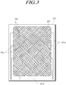
FIG. 3 is a plan view illustrating a first embodiment of a sensing unit employed in the display device illustrated inFIG. 1 ; -
FIG. 4 is a plan view illustrating a second embodiment of the sensing unit employed in the display device illustrated inFIG. 1 ; -
FIG. 5 is a plan view illustrating a third embodiment of the sensing unit employed in the display device illustrated inFIG. 1 ; -
FIG. 6 is a plan view illustrating an embodiment of a non-display region employed in the display device illustrated inFIG. 1 ; -
FIG. 7 is a cross-sectional view illustrating a first embodiment of the non-display region of the display device ofFIG. 6 taken along line A-A' inFIG. 6 ; -
FIG. 8 is a cross-sectional view illustrating the first embodiment of the non-display region ofthe display device ofFIG. 6 taken along line B-B' inFIG. 6 ; -
FIG. 9 is a cross-sectional view illustrating a second embodiment ofthe non-display region ofthe display device ofFIG. 6 taken along line A-A' inFIG. 6 ; -
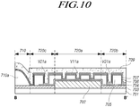
FIG. 10 is a cross-sectional view illustrating the second embodiment of the non-display region of the display device ofFIG. 6 taken along line B-B' inFIG. 6 ; -
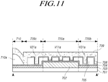
FIG. 11 is a cross-sectional view illustrating a third embodiment ofthe non-display region ofthe display device ofFIG. 6 taken along line A-A' inFIG. 6 ; -
FIG. 12 is a cross-sectional view illustrating the third embodiment of the non-display region ofthe display device ofFIG. 6 taken along line B-B' inFIG. 6 ; -
FIG. 13 is a cross-sectional view illustrating a first embodiment of the non-display region of the display device ofFIG. 6 taken along line A-A' inFIG. 6 ; -
FIG. 14 is a cross-sectional view illustrating the first embodiment of the non-display region ofthe display device ofFIG. 6 taken along line B-B' inFIG. 6 ; -
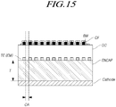
FIG. 15 is a cross-sectional view illustrating a first embodiment of a display region of the display device ofFIG. 1 ; -
FIG. 16 is a cross-sectional view illustrating a second embodiment ofthe display region of the display device ofFIG. 1 ; and -
FIG. 17 is a flowchart illustrating a method of manufacturing a display device according to the disclosure. - Hereinafter, some embodiments ofthe disclosure will be described in detail with reference to the accompanying illustrative drawings. In designating elements of the drawings by reference numerals, the same elements will be designated by the same reference numerals although they are shown in different drawings. Further, in the following description of the disclosure, a detailed description of known functions and configurations incorporated herein will be omitted when it may make the subject matter of the disclosure rather unclear.
- In addition, terms such as first, second, A, B, (a), (b) or the like may be used herein when describing components ofthe disclosure. Each of these terminologies is not used to define an essence, order or sequence of a corresponding component but used merely to distinguish the corresponding component from other component(s). In the case that it is described that a certain structural element "is connected to", "is coupled to", or "is in contact with" another structural element, it should be interpreted that a further structural element may "be connected to", "be coupled to", or "be in contact with" the structural elements as well and that the certain structural element is directly connected to or is in direct contact with the another structural element. Additionally, when an element is "on" or "above" another element, the two elements can be in direct contact or there can be one or more intermediate elements between the two elements.
-
FIG. 1 is a plan view illustrating an embodiment of a display device according to the disclosure. - Referring to
FIG. 1 , adisplay device 100 may include adisplay region 110 formed in a first region on asubstrate 102 and having a plurality of pixels (not illustrated) disposed therein, a touch electrode (not illustrated) disposed on thedisplay region 110 and configured to sense a touch, and anon-display region 120 disposed in a second region on thesubstrate 102. - The
substrate 102 may be a bendable plastic substrate. However, the disclosure is not limited thereto. - A plurality of data lines (not illustrated) and a plurality of gate lines (not illustrated) may intersect each other in the
display region 110, which may be formed with a plurality of pixels that are connected to the data lines and the gate lines. The pixel may receive a data signal transmitted through the data lines in response to a gate signal transmitted through the gate lines, and may emit light corresponding to the data signal. In addition, thedisplay region 110 may further include a power supply line (not illustrated) configured to supply driving power to the pixels. However, the disclosure is not limited thereto. - In addition, a plurality of touch electrodes may be arranged on the
display region 110. The touch electrodes may sense a touch on the display region and may generate a corresponding touch sensing signal. Accordingly, a sensing unit (not illustrated) including a plurality of touch electrodes may be arranged on thedisplay region 110 of thedisplay device 100. - The
non-display region 120 includesfirst pad portions 131a arranged in the second region of thesubstrate 102 and configured to supply pixel driving signals corresponding to the plurality of pixels;second pad portions 131b configured to supply touch sensor signals corresponding to the touch electrodes; a link portion configured to transmit a signal transmitted from thefirst pad portions 131a and thesecond pad portions 131b to thedisplay region 110 and the touch electrodes, respectively; and a wiring portion in which a wiring is arranged to interconnect the first andsecond pad portions - The
first pad portions 131a may be connected to a drive IC (not illustrated) that supplies a data signal, a gate signal and the like (which may be collectively referred to as pixel driving signals), which are related to the driving of the display region. Thesecond pad portions 131b may be connected to a touch drive IC (not illustrated) that is related to touch driving. In addtion, thesecond pad portions 131b may be disposed on the left and right of thefirst pad portions 131a. The link portion may allow the data lines and the gate lines arranged in the display region to be connected to the wirings extending from the first pad portions and the second pad portions. The wiring portion may be arranged between the link portion and the pad portions. In addition, a region of the substrate which corresponds to the wiring portion, may be a bending region that may allow the substrate to be bent. - In addition, although the
display device 100 is illustrated as including a pair offirst pad portions 131a and a pair ofsecond pad portions 131b, the disclosure is not limited thereto, and the numbers of thefirst pad portions 131 a and thesecond pad portions 131b may be determined depending on the size and resolution of thedisplay region 110. In addition, it is illustrated that there are provided a plurality offirst pad portions 131 a and twosecond pad portions 131b, but the disclosure is not limited thereto. - The
display device 100 may have a bezel region (not illustrated) where a bezel is located on the rim ofthedisplay region 110. Thenon-display region 120 may be disposed in the bezelregion, and the pad portions, to which a driver IC, a touch driver IC, and the like are connected, and a wiring that is connected to the link portion from the pad portions, the link portion, and so on maybe arranged in the non-display region. Accordingly, when thenon-display region 120 is bent, the bezel region may be implemented to have a reduced width. As a result, the effect of a narrow bezel can be further increased. In addition, since thedisplay device 100 includes dual wirings including a first wiring and a second wiring in the bending region, no obstacle is presented to the transmission of a signal even if thesubstrate 102 is bent and a crack is generated in one of the first and second wirings. As a result, the width ofthe wiring may be reduced to be applicable to a high-resolution display device. -
FIG. 2 is a cross-sectional view illustrating an embodiment ofthe display device illustrated inFIG. 1 . - Referring to
FIG. 2 , thedisplay device 200 may include adisplay panel 201 and asensing unit 240, and thesensing unit 240 may be disposed on thedisplay panel 201. In addition, thedisplay device 200 may include abending region 220a in which one region is bent. In addition, thedisplay panel 201 may be divided into adisplay region 210 andnon-display regions non-display areas link portion 220c, abending region 220a, and apad portion 220b. Among thenon-display regions pad portion 220b may be disposed below other portions of the display panel 201 (e.g. below thelink region 220c or display region 210) due to thebending region 220a, so that the bezel region can be implemented to be thinner in comparison with the case in which the pad portion is not located below thelink region 220c ordisplay region 210. -
FIG. 3 is a plan view illustrating a first embodiment of a sensing unit employed in the display device illustrated inFIG. 1 . - Referring to
FIG. 3 , the sensing unit may be disposed on adisplay panel 301, and may include a plurality of first electrodes TEa and a plurality of second electrodes TEb. The plurality of first electrodes TEa may correspond to touch driving electrodes TEa and the plurality of second electrodes TEb may correspond to touch sensing electrodes TEb. The plurality of first electrodes TEa may be connected in the horizontal direction by the connection part s 322 so as to form a plurality of electrode rows, and the plurality of second electrodes TEb may be connected in the vertical direction by theconnection part 322 so as to form a plurality of electrode columns. Here, the plurality of first electrodes TEa and the plurality of second electrodes TEb are illustrated as being arranged in a 4 x 3 form, but this embodiment is not limited thereto. - The first electrodes TEa may receive a touch driving signal, and the second electrodes TEb may transmit a touch sensing signal that corresponds to the touch driving signal The first electrodes TEa and the second electrodes TEb may be formed on the same layer on the
display panel 301. However, this embodiment is not limited thereto. - The
connection parts 322 may allow one first electrode TEa to be connected to the other first electrodes, and one second electrode TEb to be connected to the other second electrodes. Theconnection parts 322 intersect each other. In order to ensure that the first electrodes TEa and the second electrodes TEb are not directly connected to each other, theconnection parts 322 that connect the first electrodes TEa to each other may be formed in a layer that is different from the layer in which the first electrodes TEa and the second electrodes TEb are formed, and the first electrodes TEa and the connection parts may be connected to each other through vias. Theconnection parts 322 that connect the second electrodes TEb to each other may be formed in a layer that is the same as the layer in which the first electrodes TEa and the second electrodes TEb are formed, so that the second electrodes TEb can be connected in the same layer. Accordingly, an insulating film (not illustrated) may be disposed between theconnection parts 322 that connect the first electrodes TEa and theconnection parts 322 that connect the second electrodes TEb. - In addition, the first electrodes TEa and the second electrodes TEb may be formed by patterning a conductive metallic layer. The first electrodes TEa and the second electrodes TEb may be formed of a transparent material, such as Indium Tin Oxide (ITO). In addition, the patterned first electrodes TEa and second electrodes TEb may include an electrode pattern formed in the form of a mesh, and the first electrodes TEa and the second electrodes TEb may have a plurality of openings. Light, which is emitted from the display device through the first electrodes TEa and the second electrodes TEb made of the ITO electrodes or the plurality of openings included in the first electrodes TEa and the second electrodes TEb, may be transmitted through the first electrodes TEa and the second electrodes TEb, or maybe emitted to the outside through the plurality of openings.
- The patterns of the first electrodes TEa and the second electrodes TEb formed in the form of a mesh may be referred to as a touch electrode wiring. In addition, the first electrodes TEa and the second electrodes TEb may be connected to driving
lines 321 a that cause a driving signal which drives the first electrodes TEa and the second electrode TEb, to be applied to a touch electrode, and sensinglines 321b that cause a sensing signal, which is generated in response to a touch sensed by the touch electrode, to be transmitted. Thedriving lines 321a and thesensing lines 321b may be referred to as touch wirings. In addition, the touch wirings including the drivinglines 321 a and thesensing lines 321b may be respectively connected to the second pad portions illustrated inFIG. 1 . -
FIG. 4 is a plan view illustrating a second embodiment ofthe sensing unit employed in the display device illustrated inFIG. 1 . - Referring to
FIG. 4 , the sensing unit may be disposed on thedisplay panel 401, and a plurality of touch electrodes TE each having a predetermined area may be arranged in a matrix formed on thedisplay panel 401. In addition, a plurality oftouch wirings 420 may be respectively connected to the touch electrodes TE so as to receive a touch sensing signal from the touch electrodes TE. The touch wirings 420 are disposed under the touch electrodes and may be in contact with a region of the touch electrodes TE. The touch electrodes TE and the touch wirings 420 may be mounted in thedisplay panel 401, and as a result, when thedisplay device 401 is made not to include a separate touch panel on thedisplay panel 401, thedisplay panel 401 may be implemented to be thinner. -
FIG. 5 is a plan view illustrating a third embodiment of the sensing unit employed in the display device illustrated inFIG. 1 . - Referring to
FIG. 5 , the sensing unit may be disposed on thedisplay panel 501, and may include first touch electrodes TEd1, TEd2, ..., TEdn-1, and TEdn arranged in the vertical direction on thedisplay panel 501, and second touch electrodes TES1, TES2, ..., TESm-1, and TESm disposed on thedisplay panel 501 and arranged in the horizontal direction. In addition, the first touch electrodes TEd1, TEd2, ..., TEdn-1 and TEdn arranged in the vertical direction may be called touch driving electrodes, and the second touch electrodes TES1, TES2, ..., TESm-1, and TESm may be called touch sensing electrodes. In addition, an insulating film (not illustrated) may be disposed between the first touch electrodes TEd1, TEd2, ..., TEdn-1, TEdn and the second touch electrodes TES1, TES2, ..., TESm-1, and TESm, so that the first touch electrodes TEd1, TEd2, ..., TEdn-1, TEdn and the second touch electrodes TEs1, TEs2, ..., TEsm-1, TEsm can be capacitively coupled to each other. In addition, the sensing unit can sense a change in capacitance caused between the first touch electrodes TEd1, TEd2, ..., TEdn-1, and TEdn and the second touch electrodes TES1, TES2, ..., TESm-1, and TESm by a touch in order to detect a touch position. -
FIG. 6 is a plan view illustrating an embodiment of a non-display region employed in the display device illustrated inFIG. 1 . - Referring to
FIG. 6 , the non-display region A may include apad portion 620b, alink portion 620c, and awiring portion 620a. - The
pad portion 620b may be divided into afirst pad portion 631 a and asecond pad portion 631b, in which thefirst pad portion 631a may receive a signal that is to be applied to a plurality of pixels arranged in thedisplay region 610, and thesecond pad portion 631 b may receive a signal that is to be applied to the touch electrodes. Thelink portion 620c transmits the received signals to the pixels or touch electrodes. Thewiring portion 620a interconnects thepad portion 620b and thelink portion 620c and transmits signals from thepad portion 620b to thelink portion 620c. Thewiring portion 620a may be disposed in the bending region to be bent. A first wiring and a second wiring on the first wiring may be disposed in thewiring portion 620a. In addition, the second wiring may not be disposed on the first wiring in portions of thelink portion 620c. The second wiring may be disposed above the first wiring that is disposed in thepad portion 620b and thewiring portion 620a. In addition, the second wiring may include a ring-shaped pattern having an empty central region in order to prevent the second wiring from being completely cut offeven if a crack is generated in the second wiring. Even if a crack is generated in the second wiring, the crack can be prevented from propagating by the empty central region of the ring shape in which no wiring is deposited. Accordingly, even if the substrate is bent and as a result a crack is generated in the second wiring, it is possible to reduce the frequency of complete cut-off caused in the second wiring. For example, the ring-shaped pattern may be a pattern having a rectangular ring shape, diamond ring shape, or circular ring shape, or other types of ring shapes. However, this embodiment is not limited thereto. In addition, the first wiring may be formed with a ring-shaped pattern to correspond to the shape of the second wiring pattern. - In addition, since the
wiring portion 620a has dual wirings configured with the first wiring and the second wiring, even if one wiring is cut off, the other wiring can be prevented from being cut off, and as a result, it is possible to implement the wiring to have a reduced width. Therefore, it can be easily applied to a display device having a high resolution. -
FIG. 7 is a cross-sectional view illustrating a first embodiment of the non-display region of the display device ofFIG. 6 taken along line A-A' inFIG. 6 .FIG. 8 is a cross-sectional view illustrating the first embodiment of the non-display region of the display device ofFIG. 6 taken along line B-B' inFIG. 6 . - The display device may include: a
substrate 701 divided into adisplay region 710 andnon-display regions 720a (e.g. wiring region), 720b (e.g. pad region), and 720c (e.g. link region); a firstorganic film 702 disposed in oneofthe non-display regions first wiring 704 formed in a predetermined pattern on thesubstrate 701 on which the firstorganic film 702 is disposed; a secondorganic film 705 formed on thefirst wiring 704 and formed with via holes V11a, V21a, and V31a that cause thefirst wiring 704 to be exposed; andsecond wirings first wiring 704 in a predetermined pattern and connected to thefirst wiring 704 at one or more spaced apart locations above the firstorganic film 702 that correspond to the via holes V11a, V21a, and V31a. - Referring to
FIG. 7 , the firstorganic film 702 may be formed on asubstrate 701, and thefirst wiring 704 may be deposited on thesubstrate 701 having the firstorganic film 702 formed thereon. Thesubstrate 701 may be a plastic substrate. Thefirst wiring 704 extends to thedisplay region 710 and is electrically connected to the pixels because thefirst wiring 704 is a wiring for supplying signals to the pixels disposed in thedisplayregion 710. The firstorganic film 702 may be formed when depositing a gate insulating film formed before the gate electrodes of transistors formed in the pixels are formed. In addition, abuffer layer 703 may be formed between thesubstrate 701 and thefirst wiring 704. Thebuffer layer 703 is made from a different material than theorganic film 702. Further, thefirst wiring 704 may be a source/drain metal forming source and drain electrodes of a transistor. The firstorganic film 702 may be formed at a position corresponding to the bending region ofthesubstrate 701. Since the firstorganic film 702 is formed of a soft material, it can flex smoothly when thesubstrate 701 is bent so that a crack can be prevented from being generated in thefirst wiring 704. - In addition, a second
organic film 705 may be formed on thefirst wiring 704 and one or more via holes V11a, V21 a, and V31 a may be formed therein. Thefirst wiring 704 and thesecond wirings first wiring 704 is separated from thesecond wirings organic film 705 at multiple locations such that thefirst wiring 704 is a predetermined distance from thesecond wirings first wiring 704 and thesecond wirings first wiring 704 and thesecond wiring first wiring 704 and thesecond wirings first wiring 704 and thesecond wirings second wirings organic film 705 and may not extend past the edge of the secondorganic film 705 in thelink portion 720c. Via hole V11a is formed in the secondorganic film 705 above the firstorganic film 702 and above thefirst wiring 704. Via holes V21a and V31a are formed above thefirst wiring 704 but not above the firstorganic film 702. However, without being limited thereto, the via holes V11a may be formed only above the firstorganic film 702. Also, one or more via holes V11a may be formed above the firstorganic film 702. - Then, a third
organic film 709 may be deposited on the second wirings 706,707, and 708. - Referring to
FIG. 8, FIG. 8 illustrates a cross section of a second pad portion that transmits touch signals to touch electrodes and a touch wiring that applies signals to the touch electrodes. The structure illustrated inFIG. 8 is different from that illustrated inFIG. 7 in that, since signals are applied to the touch electrodes, thefirst wiring 704 is formed only up to a region of thelink portion 720c in the non-display region, while thesecond wirings display region 710 and may become touch electrodes. Thus, thesecond wirings display region 710, an in-cap substrate 710a may be disposed on thesubstrate 701. Accordingly, the touch electrodes formed by thesecond wires cap substrate 710a, so that it is possible to include a sensing unit in the display device by arranging the touch electrodes without using a separate touch panel. However, this embodiment is not limited thereto, and a transistor, a light-emitting layer, an electrode, and the like may be further formed between thesubstrate 701 and the in-cap substrate 710a. - In addition, the third
organic film 709 deposited on thesecond wirings display region 710, so that the upper portion of thedisplay region 710 is planarized. - Further, the
second wirings first metal layer 706, an insulatingfilm 707 disposed on thefirst metal layer 706, and asecond metal layer 708 on which the insulatingfilm 707 is disposed. Thefirst metal layer 706 may correspond to the metal layer forming theconnection parts 322 in the sensing unit illustrated inFIG. 3 , and thesecond metal layer 708 may correspond to the metal layer forming the first electrode TEa and the second electrode TEb in the sensing unit illustrated inFIG. 3 . Further, the insulatingfilm 707 may be an insulating film disposed between the first and second electrodes TEa and TEb and theconnection parts 322. Further, thefirst metal layer 706 may be thetouch wiring 420 illustrated inFIG. 4 , thesecond metal layer 708 may be the touch electrode TE illustrated inFIG. 4 , and the insulating film is disposed between the touch electrode wiring and the touch electrodes. Further, thefirst metal layer 706 may correspond to the metal layer forming the first touch electrodes TEd1, TEd2, ..., TEdn-1, and TEdn illustrated inFIG. 5 , and thesecond metal layer 708 may correspond to the metal layer forming the second electrodes TES1, TES2, ..., TESm-1, and TESm. Further, the insulatingfilm 707 may correspond to the insulating film disposed between the first touch electrodes TEd1, TEd2, ..., TEdn-1, and TEdn and the second touch electrodes TES1, TES2, ..., TESm-1, and TESm illustrated inFIG. 5 . - However, this embodiment is not limited thereto. The second wiring may include a
first metal layer 706 and an insulatingfilm 707 disposed on thefirst metal layer 706, as illustrated inFIG. 9 or10 . - In addition, as illustrated in
FIG. 11 or12 , the second wiring may be formed of afirst metal layer 706. -
FIG. 13 is a cross-sectional view illustrating a first embodiment of the non-display region of the display device ofFIG. 6 taken along line A-A' inFIG. 6 .FIG. 14 is a cross-sectional view illustrating the first embodiment of the non-display region of the display device ofFIG. 6 taken along line B-B' inFIG. 6 . - The display device may include a
substrate 701 divided into adisplay region 710 and non -display regions 720a (e.g. wiring region), 720b (e.g. pad region), and 720c (e.g. link region); a firstorganic film 702 disposed partly in one of thenon-display regions organic film 702 includes afirst portion 702a and asecond portion 702b and thefirst portion 702a is located in thedisplay region 710 and thesecond portion 702b is located in one of thenon-display regions organic film 702 is located between thefirst portion 702a and thesecond portion 702b of the firstorganic film 702; afirst wiring 704 formed in a predetermined pattern on thesubstrate 701 on which the firstorganic film 702 is disposed; a secondorganic film 705 formed on thefirst wiring 704 and formed with via holes V11a, V21a, and V31a that cause thefirst wiring 704 to be exposed ; andsecond wirings first wiring 704 in a predetermined pattern and connected to thefirst wiring 704 at one or more spaced apart locations above the firstorganic film 702 that correspond to the via holes V11a, V21a, and V31a. - Referring to
FIGs. 13 and14 , the firstorganic film 702 may be formed on thesubstrate 701, and thefirst wiring 704 may be deposited on thesubstrate 701 having the firstorganic film 702 formed thereon. Thesubstrate 701 may be a plastic substrate. Thefirst wiring 704 extends over the second portion of the firstorganic film 702 in thenon-display region organic film 702. Thefirst wiring 704 carry a signal to thedisplay region 710 and is electrically connected to the pixels because thefirst wiring 704 is a wiring for supplying signals to the pixels disposed in thedisplay region 710. - In addition, the second
organic film 705 may be formed on thefirst wiring 704 and one or more via holes V11a, V21a, and V31a may be formed therein. Thefirst wiring 704 and thesecond wirings first wiring 704 is separated from thesecond wirings organic film 705 at multiple locations such that thefirst wiring 704 is a predetermined distance from thesecond wirings first wiring 704 and thesecond wirings first wiring 704 and thesecond wiring second wiring 706 on the secondorganic film 705 that is electrically connected to thefirst wiring 704 in thenon-display region -
FIG. 15 is a cross-sectional view illustrating a first embodiment of a display region of the display device illustrated inFIG. 1 .FIG. 16 is a cross-sectional view illustrating a second embodiment ofthe display region of the display device ofFIG. 1 . - The touch electrodes TE may be formed in the display device. The touch electrodes may be made from electrode metal (EM). Here, the display device may be an OLED display device using OLEDs, and when the touch electrodes TE are formed in the display device, the touch electrodes may be positioned between an encapsulation layer ENCAP and a display cover (not shown). Also, the touch electrodes TE may be a plurality of electrodes and a plurality of signal lines having a plurality of electrode patterns.
- Further, as illustrated in
FIG. 15 , the touch electrodes TE may be disposed on the encapsulation layer ENCAP, and as illustrated inFIG. 16 , the touch electrodes TE may be disposed on the overcoat layer OC. That is, the touch electrodes TE may be included in the display device without using a separate touch panel. The encapsulation layer ENCAP has a thickness T and is disposed on a cathode. - Referring to
FIG. 15 , the touch electrodes TE may be formed on the encapsulation layer ENCAP, and an overcoat layer OC may be formed on the touch electrodes TE. In addition, a black matrix BM may be disposed on the overcoat layer OC at a position corresponding to the touch electrodes TE, and color filters CF may be disposed above the black matrix BM. A display cover (not illustrated) maybe disposed on the color filters CF. - As described above, by forming the touch electrodes TE on the encapsulation layer ENCAP, the touch electrodes TE can be formed without greatly affecting the display performance and the formation of the layer for the display.
- Meanwhile, in the case of a touch sensing method of a mutual capacitance type, connection parts for connecting the driving electrodes and/or the sensing electrodes may exist among the plurality of touch electrodes TE. The connection parts may be present in a layer that is different from the layer ofthe touch electrodes TE with an insulating layer interposed therebetween.
- Meanwhile, referring to
FIG. 15 , a cathode of one or more Organic Light-Emitting Diodes (OLED) may exist under the encapsulation layer ENCAP. - The thickness T ofthe encapsulation layer ENCAP may be, for example, 5 micrometers or more.
- Parasitic capacitance formed between the cathode ofthe OLED and the touch electrodes TE may be reduced by designing the thickness (T) of the encapsulation layer ENCAP to be 5 micrometers or more. Thus, it is possible to prevent deterioration in touch sensitivity due to paras itic capacitance.
- On the other hand, when the touch electrodes TE are formed of a mesh-type electrode metal EM having open regions OA, the position of each of the open regions OA may correspond to one or two or more sub-pixels or the positions of light-emitting units when viewed in the vertical direction.
- Therefore, as illustrated in
FIG. 15 , the plurality of open regions OA may correspond to the plurality of color filters CF. - As described above, in an OLED display device, it is possible to provide a display device having excellent light-emitting performance by arranging the color filters CF, which are necessary in the case where white OLEDs or the like are used, to correspond to the open regions OA.
- The vertical positional relationship between the color filters CF and the touch electrodes TE will now be described.
- As described above, it is possible to provide a
touch display device 100 having an optimal positional relationship between the cobr filters CF and the touch electrodes TE in consideration of display performance, such as light-emitting performance, and touch performance. - Meanwhile, attempts to incorporate a touch panel including touch electrodes TE in a
display panel 110 have been made in order to improve manufacturing convenience ofthetouch display device 100 and to reduce the size ofthetouch display device 100. - However, there are considerable difficulties and many constraints in order to incorporate sensing units TSP in a display device. For example, during the process of manufacturing a display device, there is a limit in that a high-temperature process for forming touch electrodes TE, which are generally made of a metallic material, inside a panel cannot be freely performed due to the presence of an organic material. Therefore, when the touch electrodes TE are formed on the overcoat layer OC, a high-temperature process can be performed more freely.
- Referring to
FIG. 16 , a black matrix may be formed on the encapsulation layer ENCAP, and color filters CF may be disposed on the black matrix BM. The overcoat layer OC may be formed on the color filters CF. In addition, the electrode pattern ofthe touch electrodes TE may be disposed on the overcoat layer OC at the positions corresponding to the black matrix BM. A display cover (not illustrated) may be disposed on the color filters CF. - Meanwhile, in the case of a touch sensing method of a mutual capacitance type, there may be connection parts for connecting the driving electrodes and/or the sensing electrodes, among the plurality of touch electrodes TE. The connection parts may be present in a layer that is different from the layer ofthe touch electrodes TE with an insulating layer interposed therebetween.
-
FIG. 17 is a flowchart illustrating a method of manufacturing a display device according to the disclosure. - Referring to
FIG. 17 , a method of manufacturing a display device may form a first organic film on a substrate (S1500). The first organic film may be formed corresponding to a bending region to be bent in a non-display region. - Then, the first wiring may be deposited and patterned on the first organic film (S1510). The first wiring may be a source drain metal that supplies a signal to a pixel formed in a display region. Further, when the first wiring is a wiring configured to supply a signal to the display region, the first wiring may extend to the display region. However, when the first wiring is a wiring configured to supply a signal to the touch electrode, the first wiring may be formed only in the non-display region without extending to the display region.
- Then, a second organic film may be deposited above the first wiring, at least one via hole may be formed in the second organic film so as to cause the first wiring to be exposed above an upper side of the first organic film, and a second wiring may be deposited and patterned above the second organic film, and the second wiring may be connected to the first wring via the via hole (S1520). The second wiring may be formed to have a ring-shaped pattern. Even if cracks occur in the second wiring due to the ring shape, the cracks occurring in the ring shape can be prevented from cutting off the entire ring shape owing to the central region of the ring shape in which no metal layer is formed. Also, since it is possible to avoid a cut-off portion by portions connected through via holes even if the first wiring or the second wiring is cut off, it is still possible to prevent a signal from failing to be transmitted even if cracks occur due to bending. Also, the greater the number of via holes, the greater the number of cracks that can be tolerated.
- The second wiring may include a plurality of metal layers. In addition, the second wiring may include a first metal layer, a second organic film disposed on the first metal layer, and a second metal layer above which the second organic film is disposed. The first metal layer may correspond to the
connection parts 322 in the sensing unit illustrated inFIG. 3 , and the second metal layer may correspond to the first electrodes TEa and the second electrodes TEb in the sensing unit illustrated inFIG. 3 . In addition, the first metal layer may correspond to thetouch wiring 420 in the sensing unit illustrated inFIG. 4 , and the second metal layer may correspond to the touch electrodes TE in the sensing unit illustrated inFIG. 4 . In addition, the first metal layer may correspond to the first electrodes TEd1, TEd2, ..., TEdn-1, and TEdn in the sensing unit illustrated inFIG. 5 , and the second metal layer may correspond to the second electrodes TEs1, TEs2, ..., TEsm-1, TEsm in the sensing unit illustrated inFIG. 5 . - When the second wiring corresponds to a wiring for supplying a signal to the display region, the second wiring may extend only to the non-display region. In addition, when the second wiring corresponds to a wiring for supplying a signal to touch electrodes, the second wiring may extend to the display region so as to correspond to the touch electrodes disposed above the display region.
- Accordingly, even if the first wiring and the second wiring are connected to each other at one point of the bending region and cracks occur in the first wiring and/or the second wiring, a signal can be transmitted.
- The above description and the accompanying drawings provide an example ofthe technical idea ofthe disclosure for illustrative purposes only. Those having ordinary knowledge in the technical field, to which the disclosure pertains, will appreciate that various modifications and changes in form, such as combination, separation, substitution, and change of a configuration, are possible without departing from the essential features of the disclosure. Therefore, the embodiments disclosed in the disclosure are intended to illustrate the scope of the technical idea of the disclosure, and the scope of the disclosure is not limited by the embodiment. The scope ofthe disclosure shall be construed on the basis of the accompanying claims in such a manner that all of the technical ideas included within the scope equivalent to the claims belong to the disclosure.
Claims (20)
- A display device comprising:a display region [610] formed in a first region on a substrate, said display region comprising a plurality of pixels on a substrate and a touch electrode configured to sense a touch; anda non-display region [620] separate from the display region and disposed on a second region of the substrate, wherein the non-display region comprises a bending region where the substrate is bent and wiring configured to carry a signal corresponding to the plurality of pixels or corresponding to the touch electrode, the wiring including:first wiring: andsecond wiring above the first wiring in the bending region and being electrically connected in the bending region to the first wiring.
- The display device of claim 1, wherein the non-display region comprises:a pad portion [620b] to receive the signal corresponding to the plurality of pixels or corresponding to the touch electrode;a link portion [620c] to transmit the signal to the plurality of pixels or to the touch electrode; anda wiring portion [620a] in the bending region and interconnecting the pad portion and the link portion, the wiring being in the wiring portion.
- The display device of claim 1 or claim 2, wherein the signal is a signal corresponding to the plurality of pixels, and the first wiring is electrically connected to the plurality of pixels.
- The display device of claim 1 or claim 2, wherein the signal is a signal corresponding to the touch electrode, and the second wiring is electrically connected to the touch electrode.
- The display device of any preceding claim, wherein the bending region comprises an organic film disposed on the first wiring,
wherein the second wiring is disposed on the organic film, and
wherein the second wiring is electrically connected to the first wiring through a hole in the organic film. - The display device of claim 5, wherein the bending region includes another organic film disposed above the substrate, wherein the first wiring is disposed above the another organic film.
- The display device of any preceding claim, wherein the second wiring is electrically connected in the bending region to the first wiring at a plurality of spaced apart locations.
- The display device of claim 7, further comprising a plurality of via holes at the spaced apart locations and the second wiring is electrically connected to the first wiring through the via holes.
- The display device of any preceding claim, wherein the second wiring includes a first metal layer [706] and an insulating film [707] disposed on the first metal layer.
- The display device of claim 9, wherein the second wiring further includes a second metal layer [708] disposed above the insulating film.
- The display device of any preceding claim, wherein at least one of the first wiring and the second wiring has a ring-shaped pattern in the bending region.
- The display device of any preceding claim, wherein the display region comprises:a cathode corresponding to one or more organic light emitting diodes, OLEDs; andan encapsulation layer on the cathode,wherein the touch electrode is disposed on the encapsulation layer.
- A display device comprising:a substrate divided into a display region and a non-display region;a first organic film [702] disposed in the non-display region;a first wiring [704] in a predetermined pattern on the first organic film in the non-display region;a second organic film [705] above the first wiring, a via hole in the second organic film exposing a portion of the first wiring; anda second wiring in a predetermined pattern above the first wiring and electrically connected to the first wiring at one or more locations, at least one of the locations corresponding to the via hole.
- The display device of claim 13, further comprising:a cathode layer corresponding to one or more organic light emitting diodes, OLEDs, on the substrate in the display region;an encapsulation layer disposed on cathode layer; anda touch electrode on the encapsulation layer,wherein the second wiring and the touch electrode are in a same metal layer
- The display device of claim 13 or claim 14, wherein the second wiring includes a first metal layer and an insulating film disposed on the first metal layer.
- The display device of claim 15, wherein the second wiring further includes a second metal layer disposed above the insulating film.
- The display device of any of claims 13-16, wherein the pre-determined pattern is a ring-shaped pattern.
- A display device, comprising:a substrate;a first organic film on the substrate, the first organic film having a first portion located in a display area and a second portion located in a non-display area, an opening in the first organic film located between the first portion and the second portion of the first organic film; andfirst wiring to carry a signal to the display area, the first wiring extending over the second portion of the first organic film in the non-display area and also extending over the opening in the first organic film.
- The display device of claim 18, further comprising:a second organic film on the first wiring; andsecond wiring on the second organic film that is electrically connected to the first wiring in the non-display area.
- The display device of claim 19, wherein the second wiring is electrically connected to the first wiring through holes in the second organic film.
Applications Claiming Priority (1)
| Application Number | Priority Date | Filing Date | Title |
|---|---|---|---|
| KR1020170068424A KR102409200B1 (en) | 2017-06-01 | 2017-06-01 | Display apparatus including touch electrode and maunufacturing method for the same |
Publications (2)
| Publication Number | Publication Date |
|---|---|
| EP3410272A1 true EP3410272A1 (en) | 2018-12-05 |
| EP3410272B1 EP3410272B1 (en) | 2023-10-11 |
Family
ID=60782109
Family Applications (1)
| Application Number | Title | Priority Date | Filing Date |
|---|---|---|---|
| EP17210278.2A Active EP3410272B1 (en) | 2017-06-01 | 2017-12-22 | Display device including touch electrode and method for maunufacturing the same |
Country Status (6)
| Country | Link |
|---|---|
| US (1) | US10845933B2 (en) |
| EP (1) | EP3410272B1 (en) |
| JP (2) | JP6552594B2 (en) |
| KR (2) | KR102409200B1 (en) |
| CN (1) | CN108984012B (en) |
| TW (1) | TWI661551B (en) |
Families Citing this family (18)
| Publication number | Priority date | Publication date | Assignee | Title |
|---|---|---|---|---|
| KR102409200B1 (en) | 2017-06-01 | 2022-06-15 | 엘지디스플레이 주식회사 | Display apparatus including touch electrode and maunufacturing method for the same |
| KR102370406B1 (en) | 2017-07-10 | 2022-03-07 | 삼성디스플레이 주식회사 | Organic light emitting display device and a method of manufacturing organic light emitting display device |
| CN107910336B (en) * | 2017-11-30 | 2019-07-02 | 昆山国显光电有限公司 | Array substrate, method for manufacturing the same, and display screen |
| KR102464252B1 (en) * | 2018-03-06 | 2022-11-08 | 삼성디스플레이 주식회사 | Touch sensor |
| JP7062490B2 (en) * | 2018-03-29 | 2022-05-06 | 株式会社ジャパンディスプレイ | Display device |
| CN109300938B (en) * | 2018-08-30 | 2021-01-26 | 京东方科技集团股份有限公司 | Display panel, preparation method thereof and display device |
| WO2020090725A1 (en) | 2018-10-31 | 2020-05-07 | 曙ブレーキ工業株式会社 | Sintered friction material and method for producing sintered friction material |
| CN109752421B (en) * | 2019-01-31 | 2021-08-24 | 厦门天马微电子有限公司 | Display panel and display device |
| US12287930B2 (en) | 2019-04-24 | 2025-04-29 | Samsung Display Co., Ltd. | Non-rigid device and display device |
| CN110085643B (en) * | 2019-04-29 | 2021-08-03 | 昆山国显光电有限公司 | Array substrate and display device |
| KR102709147B1 (en) | 2019-05-24 | 2024-09-26 | 삼성디스플레이 주식회사 | Display device |
| KR102792468B1 (en) | 2019-07-24 | 2025-04-08 | 엘지디스플레이 주식회사 | Display apparatus having touch electrodes |
| KR102862585B1 (en) * | 2019-11-04 | 2025-09-23 | 삼성디스플레이 주식회사 | Sensing structure |
| CN110797352B (en) * | 2019-11-08 | 2022-10-28 | 京东方科技集团股份有限公司 | Display panel, manufacturing method thereof and display device |
| JP7664292B2 (en) * | 2021-01-26 | 2025-04-17 | 富士フイルム株式会社 | Conductive member for touch panel, touch panel, touch panel display device, and method for manufacturing conductive member for touch panel |
| US12426454B2 (en) | 2021-05-27 | 2025-09-23 | Chengdu Boe Optoelectronics Technology Co., Ltd. | Display substrate and display device |
| KR102877626B1 (en) * | 2021-07-29 | 2025-10-28 | 엘지디스플레이 주식회사 | Display panel |
| KR20250071980A (en) * | 2023-11-15 | 2025-05-23 | 엘지디스플레이 주식회사 | Display device and method for fabricating the same |
Citations (7)
| Publication number | Priority date | Publication date | Assignee | Title |
|---|---|---|---|---|
| EP2513764A2 (en) * | 2009-12-16 | 2012-10-24 | 3M Innovative Properties Company | Touch sensitive device with multilayer electrode having improved optical and electrical performance |
| WO2016057231A1 (en) * | 2014-10-10 | 2016-04-14 | Apple Inc. | Signal trace patterns for flexible substrates |
| US20160179229A1 (en) * | 2014-12-22 | 2016-06-23 | Lg Display Co., Ltd. | Flexible Organic Light Emitting Diode Display Device |
| US20170010720A1 (en) * | 2014-05-16 | 2017-01-12 | Fujifilm Corporation | Conductive sheet for touch panel and capacitive touch panel |
| US20170062760A1 (en) * | 2015-08-24 | 2017-03-02 | Samsung Display Co, Ltd. | Flexible display and manufacturing method thereof |
| US20170090661A1 (en) * | 2015-09-30 | 2017-03-30 | Lg Display Co., Ltd. | Touch screen panel and display device comprising the same |
| KR101740192B1 (en) * | 2016-05-31 | 2017-05-25 | 엘지디스플레이 주식회사 | Organic light emitting display panel |
Family Cites Families (26)
| Publication number | Priority date | Publication date | Assignee | Title |
|---|---|---|---|---|
| US9134867B2 (en) | 2010-12-09 | 2015-09-15 | Sharp Kabushiki Kaisha | Touch panel, display device including the touch panel, and method of manufacturing the touch panel |
| JP5957846B2 (en) | 2011-10-13 | 2016-07-27 | ソニー株式会社 | DRIVE CIRCUIT BOARD, MANUFACTURING METHOD THEREOF, DISPLAY DEVICE AND ELECTRONIC DEVICE |
| KR101950833B1 (en) * | 2011-12-30 | 2019-02-22 | 엘지디스플레이 주식회사 | Organic Light Emitting Display Device |
| US9195108B2 (en) | 2012-08-21 | 2015-11-24 | Apple Inc. | Displays with bent signal lines |
| KR102007662B1 (en) * | 2012-09-20 | 2019-08-06 | 엘지디스플레이 주식회사 | Display device having minimizded bezel |
| KR101965257B1 (en) | 2012-10-08 | 2019-04-04 | 삼성디스플레이 주식회사 | Flexible display apparatus |
| CN203250289U (en) * | 2012-12-27 | 2013-10-23 | 宸鸿光电科技股份有限公司 | touch panel |
| KR102222680B1 (en) * | 2013-02-01 | 2021-03-03 | 엘지디스플레이 주식회사 | Flexible display substrate, flexible organic light emitting display device and method for manufacturing the same |
| KR101796812B1 (en) * | 2013-02-15 | 2017-11-10 | 엘지디스플레이 주식회사 | Flexible organic light emitting display device and method of manufacturing the same |
| TWI790673B (en) | 2013-03-07 | 2023-01-21 | 日商半導體能源研究所股份有限公司 | Electronic device |
| US9209207B2 (en) * | 2013-04-09 | 2015-12-08 | Apple Inc. | Flexible display with bent edge regions |
| KR102066087B1 (en) | 2013-05-28 | 2020-01-15 | 엘지디스플레이 주식회사 | Flexible display device and manufacturing method of the same |
| KR102271659B1 (en) | 2014-08-29 | 2021-06-30 | 엘지디스플레이 주식회사 | In-cell type touch panel integrated organic light emitting display apparatus |
| KR102240937B1 (en) | 2014-10-10 | 2021-04-15 | 삼성디스플레이 주식회사 | Display device |
| US9356087B1 (en) * | 2014-12-10 | 2016-05-31 | Lg Display Co., Ltd. | Flexible display device with bridged wire traces |
| US9379355B1 (en) | 2014-12-15 | 2016-06-28 | Lg Display Co., Ltd. | Flexible display device having support layer with rounded edge |
| US9773853B2 (en) * | 2015-01-09 | 2017-09-26 | Apple Inc. | Organic light-emitting diode display with bent substrate |
| KR102338753B1 (en) * | 2015-04-14 | 2021-12-15 | 삼성디스플레이 주식회사 | Touch panel and display device having the same |
| US10168844B2 (en) | 2015-06-26 | 2019-01-01 | Samsung Display Co., Ltd. | Flexible display device |
| KR102349281B1 (en) * | 2015-10-28 | 2022-01-11 | 삼성디스플레이 주식회사 | Display apparatus |
| JP6396879B2 (en) * | 2015-11-20 | 2018-09-26 | 株式会社ジャパンディスプレイ | Display device |
| KR102421600B1 (en) | 2015-11-20 | 2022-07-18 | 삼성디스플레이 주식회사 | Touch sensing unit, display device and fabrication method of the touch screen |
| TWI740908B (en) * | 2016-03-11 | 2021-10-01 | 南韓商三星顯示器有限公司 | Display apparatus |
| KR102505879B1 (en) * | 2016-03-24 | 2023-03-06 | 삼성디스플레이 주식회사 | Display apparatus |
| KR102451726B1 (en) * | 2016-03-28 | 2022-10-07 | 삼성디스플레이 주식회사 | Display device and the method of manufacturing thereof |
| KR102409200B1 (en) | 2017-06-01 | 2022-06-15 | 엘지디스플레이 주식회사 | Display apparatus including touch electrode and maunufacturing method for the same |
-
2017
- 2017-06-01 KR KR1020170068424A patent/KR102409200B1/en active Active
- 2017-11-15 US US15/814,111 patent/US10845933B2/en active Active
- 2017-12-22 EP EP17210278.2A patent/EP3410272B1/en active Active
- 2017-12-26 JP JP2017248950A patent/JP6552594B2/en active Active
- 2017-12-27 TW TW106146071A patent/TWI661551B/en active
- 2017-12-29 CN CN201711482964.4A patent/CN108984012B/en active Active
-
2019
- 2019-07-04 JP JP2019125067A patent/JP7046874B2/en active Active
-
2022
- 2022-06-10 KR KR1020220070576A patent/KR102555840B1/en active Active
Patent Citations (7)
| Publication number | Priority date | Publication date | Assignee | Title |
|---|---|---|---|---|
| EP2513764A2 (en) * | 2009-12-16 | 2012-10-24 | 3M Innovative Properties Company | Touch sensitive device with multilayer electrode having improved optical and electrical performance |
| US20170010720A1 (en) * | 2014-05-16 | 2017-01-12 | Fujifilm Corporation | Conductive sheet for touch panel and capacitive touch panel |
| WO2016057231A1 (en) * | 2014-10-10 | 2016-04-14 | Apple Inc. | Signal trace patterns for flexible substrates |
| US20160179229A1 (en) * | 2014-12-22 | 2016-06-23 | Lg Display Co., Ltd. | Flexible Organic Light Emitting Diode Display Device |
| US20170062760A1 (en) * | 2015-08-24 | 2017-03-02 | Samsung Display Co, Ltd. | Flexible display and manufacturing method thereof |
| US20170090661A1 (en) * | 2015-09-30 | 2017-03-30 | Lg Display Co., Ltd. | Touch screen panel and display device comprising the same |
| KR101740192B1 (en) * | 2016-05-31 | 2017-05-25 | 엘지디스플레이 주식회사 | Organic light emitting display panel |
Also Published As
| Publication number | Publication date |
|---|---|
| US20180348918A1 (en) | 2018-12-06 |
| KR102409200B1 (en) | 2022-06-15 |
| KR20220083998A (en) | 2022-06-21 |
| KR102555840B1 (en) | 2023-07-14 |
| US10845933B2 (en) | 2020-11-24 |
| TW201904053A (en) | 2019-01-16 |
| TWI661551B (en) | 2019-06-01 |
| JP7046874B2 (en) | 2022-04-04 |
| CN108984012B (en) | 2021-07-30 |
| CN108984012A (en) | 2018-12-11 |
| JP2019200804A (en) | 2019-11-21 |
| JP6552594B2 (en) | 2019-07-31 |
| KR20180131827A (en) | 2018-12-11 |
| EP3410272B1 (en) | 2023-10-11 |
| JP2018205687A (en) | 2018-12-27 |
Similar Documents
| Publication | Publication Date | Title |
|---|---|---|
| EP3410272B1 (en) | Display device including touch electrode and method for maunufacturing the same | |
| KR102873918B1 (en) | Touch display device | |
| TWI648670B (en) | Touch display device | |
| KR101295533B1 (en) | Liquid crystal display device and Method for manufacturing the same | |
| KR102656848B1 (en) | Display device with touch sensor and manufacturing method for the same | |
| KR102427622B1 (en) | Touch display device and touch panel | |
| US20180197924A1 (en) | Touch sensor and display device having touch sensor | |
| US20120062486A1 (en) | Display device with integrated touch screen panel and fabricating method thereof | |
| JP2019079538A (en) | Touch display panel and touch display device | |
| CN110308822A (en) | Touch display panel and preparation method thereof | |
| KR20190048985A (en) | Display device with touch sensor and manufacturing method for the same | |
| EP2827370B1 (en) | TFT-driven display device | |
| JP7609840B2 (en) | Display device | |
| KR20120045380A (en) | Touch panel, display device and manufacturing method of touch panel | |
| US10962853B1 (en) | Display substrate and display device | |
| US10845907B2 (en) | Display panel | |
| US20160103509A1 (en) | Touch display device | |
| US10921916B2 (en) | Display device | |
| KR101441525B1 (en) | Touch sensor and manufacturing method thereof |
Legal Events
| Date | Code | Title | Description |
|---|---|---|---|
| PUAI | Public reference made under article 153(3) epc to a published international application that has entered the european phase |
Free format text: ORIGINAL CODE: 0009012 |
|
| STAA | Information on the status of an ep patent application or granted ep patent |
Free format text: STATUS: REQUEST FOR EXAMINATION WAS MADE |
|
| 17P | Request for examination filed |
Effective date: 20171222 |
|
| AK | Designated contracting states |
Kind code of ref document: A1 Designated state(s): AL AT BE BG CH CY CZ DE DK EE ES FI FR GB GR HR HU IE IS IT LI LT LU LV MC MK MT NL NO PL PT RO RS SE SI SK SM TR |
|
| AX | Request for extension of the european patent |
Extension state: BA ME |
|
| RBV | Designated contracting states (corrected) |
Designated state(s): AL AT BE BG CH CY CZ DE DK EE ES FI FR GB GR HR HU IE IS IT LI LT LU LV MC MK MT NL NO PL PT RO RS SE SI SK SM TR |
|
| R17P | Request for examination filed (corrected) |
Effective date: 20171222 |
|
| STAA | Information on the status of an ep patent application or granted ep patent |
Free format text: STATUS: EXAMINATION IS IN PROGRESS |
|
| 17Q | First examination report despatched |
Effective date: 20200331 |
|
| GRAP | Despatch of communication of intention to grant a patent |
Free format text: ORIGINAL CODE: EPIDOSNIGR1 |
|
| STAA | Information on the status of an ep patent application or granted ep patent |
Free format text: STATUS: GRANT OF PATENT IS INTENDED |
|
| INTG | Intention to grant announced |
Effective date: 20230524 |
|
| GRAS | Grant fee paid |
Free format text: ORIGINAL CODE: EPIDOSNIGR3 |
|
| GRAA | (expected) grant |
Free format text: ORIGINAL CODE: 0009210 |
|
| STAA | Information on the status of an ep patent application or granted ep patent |
Free format text: STATUS: THE PATENT HAS BEEN GRANTED |
|
| AK | Designated contracting states |
Kind code of ref document: B1 Designated state(s): AL AT BE BG CH CY CZ DE DK EE ES FI FR GB GR HR HU IE IS IT LI LT LU LV MC MK MT NL NO PL PT RO RS SE SI SK SM TR |
|
| REG | Reference to a national code |
Ref country code: GB Ref legal event code: FG4D |
|
| REG | Reference to a national code |
Ref country code: CH Ref legal event code: EP |
|
| REG | Reference to a national code |
Ref country code: DE Ref legal event code: R096 Ref document number: 602017075133 Country of ref document: DE |
|
| REG | Reference to a national code |
Ref country code: IE Ref legal event code: FG4D |
|
| REG | Reference to a national code |
Ref country code: LT Ref legal event code: MG9D |
|
| REG | Reference to a national code |
Ref country code: NL Ref legal event code: MP Effective date: 20231011 |
|
| REG | Reference to a national code |
Ref country code: AT Ref legal event code: MK05 Ref document number: 1620866 Country of ref document: AT Kind code of ref document: T Effective date: 20231011 |
|
| PG25 | Lapsed in a contracting state [announced via postgrant information from national office to epo] |
Ref country code: NL Free format text: LAPSE BECAUSE OF FAILURE TO SUBMIT A TRANSLATION OF THE DESCRIPTION OR TO PAY THE FEE WITHIN THE PRESCRIBED TIME-LIMIT Effective date: 20231011 |
|
| PG25 | Lapsed in a contracting state [announced via postgrant information from national office to epo] |
Ref country code: GR Free format text: LAPSE BECAUSE OF FAILURE TO SUBMIT A TRANSLATION OF THE DESCRIPTION OR TO PAY THE FEE WITHIN THE PRESCRIBED TIME-LIMIT Effective date: 20240112 |
|
| PG25 | Lapsed in a contracting state [announced via postgrant information from national office to epo] |
Ref country code: IS Free format text: LAPSE BECAUSE OF FAILURE TO SUBMIT A TRANSLATION OF THE DESCRIPTION OR TO PAY THE FEE WITHIN THE PRESCRIBED TIME-LIMIT Effective date: 20240211 |
|
| PG25 | Lapsed in a contracting state [announced via postgrant information from national office to epo] |
Ref country code: LT Free format text: LAPSE BECAUSE OF FAILURE TO SUBMIT A TRANSLATION OF THE DESCRIPTION OR TO PAY THE FEE WITHIN THE PRESCRIBED TIME-LIMIT Effective date: 20231011 |
|
| PG25 | Lapsed in a contracting state [announced via postgrant information from national office to epo] |
Ref country code: AT Free format text: LAPSE BECAUSE OF FAILURE TO SUBMIT A TRANSLATION OF THE DESCRIPTION OR TO PAY THE FEE WITHIN THE PRESCRIBED TIME-LIMIT Effective date: 20231011 |
|
| PG25 | Lapsed in a contracting state [announced via postgrant information from national office to epo] |
Ref country code: ES Free format text: LAPSE BECAUSE OF FAILURE TO SUBMIT A TRANSLATION OF THE DESCRIPTION OR TO PAY THE FEE WITHIN THE PRESCRIBED TIME-LIMIT Effective date: 20231011 |
|
| PG25 | Lapsed in a contracting state [announced via postgrant information from national office to epo] |
Ref country code: LT Free format text: LAPSE BECAUSE OF FAILURE TO SUBMIT A TRANSLATION OF THE DESCRIPTION OR TO PAY THE FEE WITHIN THE PRESCRIBED TIME-LIMIT Effective date: 20231011 Ref country code: IS Free format text: LAPSE BECAUSE OF FAILURE TO SUBMIT A TRANSLATION OF THE DESCRIPTION OR TO PAY THE FEE WITHIN THE PRESCRIBED TIME-LIMIT Effective date: 20240211 Ref country code: GR Free format text: LAPSE BECAUSE OF FAILURE TO SUBMIT A TRANSLATION OF THE DESCRIPTION OR TO PAY THE FEE WITHIN THE PRESCRIBED TIME-LIMIT Effective date: 20240112 Ref country code: ES Free format text: LAPSE BECAUSE OF FAILURE TO SUBMIT A TRANSLATION OF THE DESCRIPTION OR TO PAY THE FEE WITHIN THE PRESCRIBED TIME-LIMIT Effective date: 20231011 Ref country code: BG Free format text: LAPSE BECAUSE OF FAILURE TO SUBMIT A TRANSLATION OF THE DESCRIPTION OR TO PAY THE FEE WITHIN THE PRESCRIBED TIME-LIMIT Effective date: 20240111 Ref country code: AT Free format text: LAPSE BECAUSE OF FAILURE TO SUBMIT A TRANSLATION OF THE DESCRIPTION OR TO PAY THE FEE WITHIN THE PRESCRIBED TIME-LIMIT Effective date: 20231011 Ref country code: PT Free format text: LAPSE BECAUSE OF FAILURE TO SUBMIT A TRANSLATION OF THE DESCRIPTION OR TO PAY THE FEE WITHIN THE PRESCRIBED TIME-LIMIT Effective date: 20240212 |
|
| PG25 | Lapsed in a contracting state [announced via postgrant information from national office to epo] |
Ref country code: SE Free format text: LAPSE BECAUSE OF FAILURE TO SUBMIT A TRANSLATION OF THE DESCRIPTION OR TO PAY THE FEE WITHIN THE PRESCRIBED TIME-LIMIT Effective date: 20231011 Ref country code: RS Free format text: LAPSE BECAUSE OF FAILURE TO SUBMIT A TRANSLATION OF THE DESCRIPTION OR TO PAY THE FEE WITHIN THE PRESCRIBED TIME-LIMIT Effective date: 20231011 Ref country code: PL Free format text: LAPSE BECAUSE OF FAILURE TO SUBMIT A TRANSLATION OF THE DESCRIPTION OR TO PAY THE FEE WITHIN THE PRESCRIBED TIME-LIMIT Effective date: 20231011 Ref country code: NO Free format text: LAPSE BECAUSE OF FAILURE TO SUBMIT A TRANSLATION OF THE DESCRIPTION OR TO PAY THE FEE WITHIN THE PRESCRIBED TIME-LIMIT Effective date: 20240111 Ref country code: LV Free format text: LAPSE BECAUSE OF FAILURE TO SUBMIT A TRANSLATION OF THE DESCRIPTION OR TO PAY THE FEE WITHIN THE PRESCRIBED TIME-LIMIT Effective date: 20231011 Ref country code: HR Free format text: LAPSE BECAUSE OF FAILURE TO SUBMIT A TRANSLATION OF THE DESCRIPTION OR TO PAY THE FEE WITHIN THE PRESCRIBED TIME-LIMIT Effective date: 20231011 |
|
| PG25 | Lapsed in a contracting state [announced via postgrant information from national office to epo] |
Ref country code: DK Free format text: LAPSE BECAUSE OF FAILURE TO SUBMIT A TRANSLATION OF THE DESCRIPTION OR TO PAY THE FEE WITHIN THE PRESCRIBED TIME-LIMIT Effective date: 20231011 |
|
| REG | Reference to a national code |
Ref country code: DE Ref legal event code: R097 Ref document number: 602017075133 Country of ref document: DE |
|
| PG25 | Lapsed in a contracting state [announced via postgrant information from national office to epo] |
Ref country code: CZ Free format text: LAPSE BECAUSE OF FAILURE TO SUBMIT A TRANSLATION OF THE DESCRIPTION OR TO PAY THE FEE WITHIN THE PRESCRIBED TIME-LIMIT Effective date: 20231011 |
|
| PG25 | Lapsed in a contracting state [announced via postgrant information from national office to epo] |
Ref country code: SK Free format text: LAPSE BECAUSE OF FAILURE TO SUBMIT A TRANSLATION OF THE DESCRIPTION OR TO PAY THE FEE WITHIN THE PRESCRIBED TIME-LIMIT Effective date: 20231011 |
|
| PG25 | Lapsed in a contracting state [announced via postgrant information from national office to epo] |
Ref country code: SM Free format text: LAPSE BECAUSE OF FAILURE TO SUBMIT A TRANSLATION OF THE DESCRIPTION OR TO PAY THE FEE WITHIN THE PRESCRIBED TIME-LIMIT Effective date: 20231011 Ref country code: SK Free format text: LAPSE BECAUSE OF FAILURE TO SUBMIT A TRANSLATION OF THE DESCRIPTION OR TO PAY THE FEE WITHIN THE PRESCRIBED TIME-LIMIT Effective date: 20231011 Ref country code: RO Free format text: LAPSE BECAUSE OF FAILURE TO SUBMIT A TRANSLATION OF THE DESCRIPTION OR TO PAY THE FEE WITHIN THE PRESCRIBED TIME-LIMIT Effective date: 20231011 Ref country code: IT Free format text: LAPSE BECAUSE OF FAILURE TO SUBMIT A TRANSLATION OF THE DESCRIPTION OR TO PAY THE FEE WITHIN THE PRESCRIBED TIME-LIMIT Effective date: 20231011 Ref country code: EE Free format text: LAPSE BECAUSE OF FAILURE TO SUBMIT A TRANSLATION OF THE DESCRIPTION OR TO PAY THE FEE WITHIN THE PRESCRIBED TIME-LIMIT Effective date: 20231011 Ref country code: DK Free format text: LAPSE BECAUSE OF FAILURE TO SUBMIT A TRANSLATION OF THE DESCRIPTION OR TO PAY THE FEE WITHIN THE PRESCRIBED TIME-LIMIT Effective date: 20231011 Ref country code: CZ Free format text: LAPSE BECAUSE OF FAILURE TO SUBMIT A TRANSLATION OF THE DESCRIPTION OR TO PAY THE FEE WITHIN THE PRESCRIBED TIME-LIMIT Effective date: 20231011 |
|
| REG | Reference to a national code |
Ref country code: CH Ref legal event code: PL |
|
| PLBE | No opposition filed within time limit |
Free format text: ORIGINAL CODE: 0009261 |
|
| STAA | Information on the status of an ep patent application or granted ep patent |
Free format text: STATUS: NO OPPOSITION FILED WITHIN TIME LIMIT |
|
| PG25 | Lapsed in a contracting state [announced via postgrant information from national office to epo] |
Ref country code: LU Free format text: LAPSE BECAUSE OF NON-PAYMENT OF DUE FEES Effective date: 20231222 |
|
| PG25 | Lapsed in a contracting state [announced via postgrant information from national office to epo] |
Ref country code: MC Free format text: LAPSE BECAUSE OF FAILURE TO SUBMIT A TRANSLATION OF THE DESCRIPTION OR TO PAY THE FEE WITHIN THE PRESCRIBED TIME-LIMIT Effective date: 20231011 |
|
| REG | Reference to a national code |
Ref country code: BE Ref legal event code: MM Effective date: 20231231 |
|
| PG25 | Lapsed in a contracting state [announced via postgrant information from national office to epo] |
Ref country code: MC Free format text: LAPSE BECAUSE OF FAILURE TO SUBMIT A TRANSLATION OF THE DESCRIPTION OR TO PAY THE FEE WITHIN THE PRESCRIBED TIME-LIMIT Effective date: 20231011 Ref country code: LU Free format text: LAPSE BECAUSE OF NON-PAYMENT OF DUE FEES Effective date: 20231222 |
|
| 26N | No opposition filed |
Effective date: 20240712 |
|
| REG | Reference to a national code |
Ref country code: IE Ref legal event code: MM4A |
|
| PG25 | Lapsed in a contracting state [announced via postgrant information from national office to epo] |
Ref country code: IE Free format text: LAPSE BECAUSE OF NON-PAYMENT OF DUE FEES Effective date: 20231222 |
|
| PG25 | Lapsed in a contracting state [announced via postgrant information from national office to epo] |
Ref country code: BE Free format text: LAPSE BECAUSE OF NON-PAYMENT OF DUE FEES Effective date: 20231231 |
|
| PG25 | Lapsed in a contracting state [announced via postgrant information from national office to epo] |
Ref country code: CH Free format text: LAPSE BECAUSE OF NON-PAYMENT OF DUE FEES Effective date: 20231231 |
|
| PG25 | Lapsed in a contracting state [announced via postgrant information from national office to epo] |
Ref country code: SI Free format text: LAPSE BECAUSE OF FAILURE TO SUBMIT A TRANSLATION OF THE DESCRIPTION OR TO PAY THE FEE WITHIN THE PRESCRIBED TIME-LIMIT Effective date: 20231011 |
|
| PG25 | Lapsed in a contracting state [announced via postgrant information from national office to epo] |
Ref country code: SI Free format text: LAPSE BECAUSE OF FAILURE TO SUBMIT A TRANSLATION OF THE DESCRIPTION OR TO PAY THE FEE WITHIN THE PRESCRIBED TIME-LIMIT Effective date: 20231011 Ref country code: IE Free format text: LAPSE BECAUSE OF NON-PAYMENT OF DUE FEES Effective date: 20231222 Ref country code: CH Free format text: LAPSE BECAUSE OF NON-PAYMENT OF DUE FEES Effective date: 20231231 Ref country code: BE Free format text: LAPSE BECAUSE OF NON-PAYMENT OF DUE FEES Effective date: 20231231 |
|
| PG25 | Lapsed in a contracting state [announced via postgrant information from national office to epo] |
Ref country code: FI Free format text: LAPSE BECAUSE OF FAILURE TO SUBMIT A TRANSLATION OF THE DESCRIPTION OR TO PAY THE FEE WITHIN THE PRESCRIBED TIME-LIMIT Effective date: 20231011 |
|
| PG25 | Lapsed in a contracting state [announced via postgrant information from national office to epo] |
Ref country code: CY Free format text: LAPSE BECAUSE OF FAILURE TO SUBMIT A TRANSLATION OF THE DESCRIPTION OR TO PAY THE FEE WITHIN THE PRESCRIBED TIME-LIMIT; INVALID AB INITIO Effective date: 20171222 |
|
| PG25 | Lapsed in a contracting state [announced via postgrant information from national office to epo] |
Ref country code: HU Free format text: LAPSE BECAUSE OF FAILURE TO SUBMIT A TRANSLATION OF THE DESCRIPTION OR TO PAY THE FEE WITHIN THE PRESCRIBED TIME-LIMIT; INVALID AB INITIO Effective date: 20171222 |
|
| PG25 | Lapsed in a contracting state [announced via postgrant information from national office to epo] |
Ref country code: TR Free format text: LAPSE BECAUSE OF FAILURE TO SUBMIT A TRANSLATION OF THE DESCRIPTION OR TO PAY THE FEE WITHIN THE PRESCRIBED TIME-LIMIT Effective date: 20231011 |
|
| PGFP | Annual fee paid to national office [announced via postgrant information from national office to epo] |
Ref country code: DE Payment date: 20251020 Year of fee payment: 9 |
|
| PGFP | Annual fee paid to national office [announced via postgrant information from national office to epo] |
Ref country code: GB Payment date: 20251023 Year of fee payment: 9 |
|
| PGFP | Annual fee paid to national office [announced via postgrant information from national office to epo] |
Ref country code: FR Payment date: 20251021 Year of fee payment: 9 |